

UC1841
UC2841
UC3841
Programmable, Off-Line, PWM Controller
• All Control, Driving, Monitoring, and
Protection Functions Included
• Low-current, Off-line Start Circuit
• Voltage Feed Forward or Current
Mode Control
• Guaranteed Duty Cycle Clamp
• PWM Latch for Single Pulse per Period
• Pulse-by-Pulse Current Limiting Plus
Shutdown for Over-Current Fault
• No Start-up or Shutdown Transients
• Slow Turn-on Both Initially and After
Fault Shutdown
• Shutdown Upon Over- or
Under-Voltage Sensing
• Latch Off or Continuous Retry After
Fault
• PWM Output Switch Usable to 1A
Peak Current
• 1% Reference Accuracy
• 500kHz Operation
• 18 Pin DIL Package
The UC1841 famil y of PWM controllers has been designed to increase
the level of versatility while retaining all of the performance features of
the earlier UC18 40 devices. Wh ile still optimized for highly-efficient bootstrapped pri mary-side operati on in forward or flyback power converters,
the UC1841 is equall y adept in impl ementing b oth low a nd high voltage
input DC to DC converters. Important performance features include a
low-current starting circuit, linear feed-forward for constant volt-second
operation, and compatibility with either voltage or current mode topologies.
In addition to start-up and normal regulating PWM functions, these devices include built in protection from over-voltage, under-voltage, and
over-current fault conditions with the option for either latch-of f or automatic restart.
While pin compatib le with the UC1840 in all respects except that the polarity of the External Stop has bee n re versed, the UC1841 offers the following improvements:
1. Fault latch reset is accomplished with slow start discharge rather
than recycling the input voltage to the chip.
2. The External Stop input can be used for a fault delay to resist
shutdown from short durat ion transients.
3. The duty-cycle clamping function has been characterized an d
specified.
The UC1841 is characteri zed for -55°C to +125°C operation while the
UC2841 and UC3841 are desi gned for -25°C to +85°C and 0°to +70°C,
respectively.
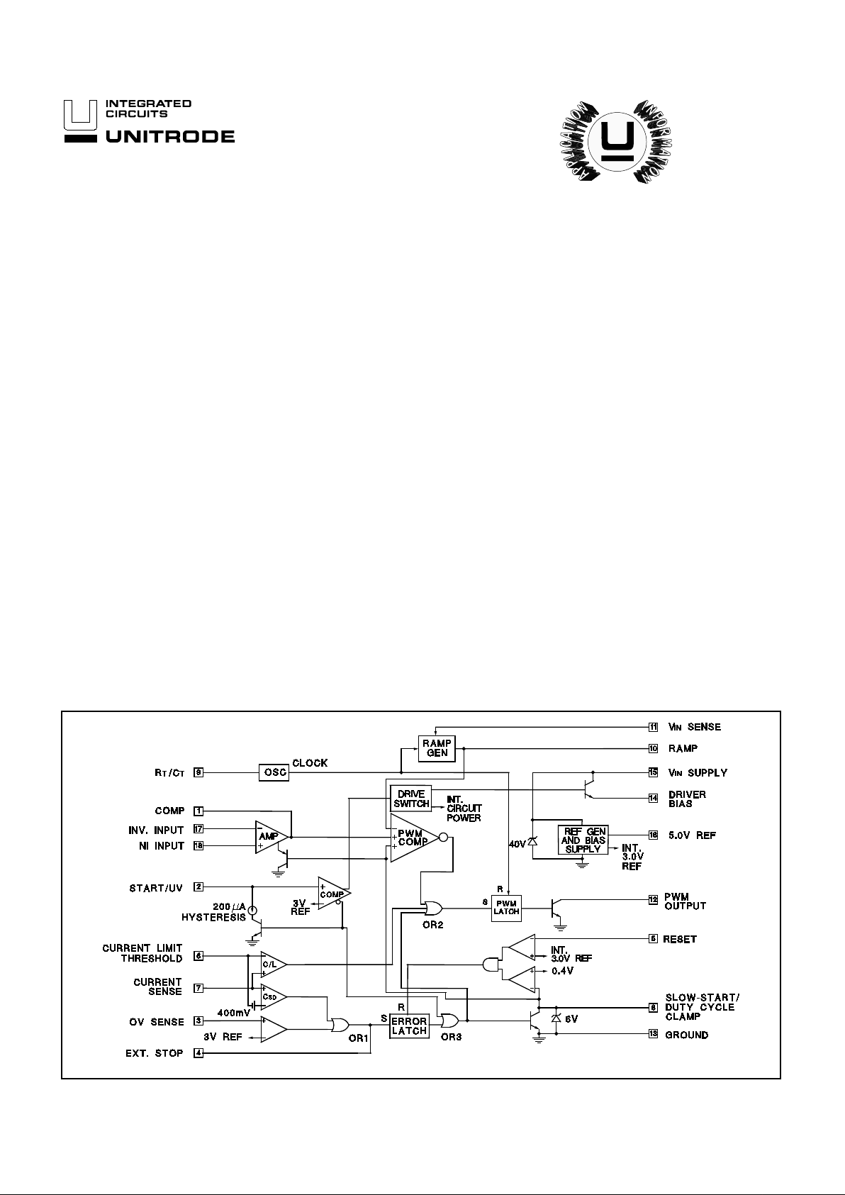
BLOCK DIAGRAM
Note: Positive tru e logic, latch out put s high with set , reset has prior ity.
6/93
DESCRIPTI ONFEATURES
PARAMETER TEST CONDITIONS
UC1841 / UC2841 UC3841 UNITS
MIN TYP MAX MIN TYP MAX
Power Inputs
Start-Up Curr ent V
IN = 30V, Pin 2 = 2.5V 4.5 6 4.5 6 mA
Operating Cur ren t V
IN = 30V, Pin 2 = 3.5V 10 14 10 14 mA
Supply OV Clamp I
IN = 20mA 33 40 45 33 40 45 V
Reference Sec tio n
Reference Voltage T
J = 25°C 4.95 5.0 5.05 4.9 5.0 5.1 V
Line Regulation V
IN = 8 to 30V 10 15 10 20 mV
Load Regulation I
L = 0 to 10mA 1020 1030mV
Temperature Stability Over Operating Temper ature Range 4.9 5.1 4 .8 5 5.15 V
Short Circuit Current V
REF = 0, TJ
= 25°C -80 -100 -80 -100 mA
Oscillator
Nominal Frequency T
J
= 25°C 47 50 53 45 50 55 kHz
Voltage Stability V
IN = 8 to 30V 0.5 1 0.5 1 %
Temperature Stability Over Operating Temper ature Range 45 55 43 57 kHz
Maximum Frequency R
T = 2kΩ, CT = 330pF 500 500 kHz
UC1841
UC2841
UC3841
ELECTRICAL CHARACTERISTICS:
Unless otherwise stated , these spec ificat ions apply for TA = -55°C to +125°C for the
UC1841, -25°C to +85°C for the UC2841, and 0°C to +70 °C for the UC3841; V
IN = 20V, RT = 20k Ω, CT = .001mfd, RR = 10kΩ,
C
R = .001mfd, Current Limit Th res hold = 200 mV, TA = TJ.
Supply Voltage, +VIN (Pin 15) (Note 2)
Voltage Driven. . . . . . . . . . . . . . . . . . . . . . . . . . . . . . . . . +32V
Current Driven, 100mA maximum. . . . . . . . . . . . Self-limiting
PWM Output Volta ge (Pin 12 ) . . . . . . . . . . . . . . . . . . . . . . . 40V
PWM Out put Current, Ste ady-State (Pin 12). . . . . . . . . 400mA
PWM Output Peak Energy Disc harge . . . . . . . . . . . . 20 µJo ules
Driver Bias Current (Pin 14). . . . . . . . . . . . . . . . . . . . . -200mA
Reference Output Current (Pin 16) . . . . . . . . . . . . . . . . -50mA
Slow-Start Sink Curren t (Pin 8) . . . . . . . . . . . . . . . . . . . . 20mA
V
IN Sense Current (Pin 11). . . . . . . . . . . . . . . . . . . . . . . . 10mA
Current Limit Input s (Pins 6 & 7) . . . . . . . . . . . . . -0. 5 to +5.5 V
Stop Input (Pin 4) . . . . . . . . . . . . . . . . . . . . . . . . . -0.3 to +5.5V
Compara to r Inputs
(Pins 1, 7, 9-1 1, 16). . . . . . . . . . . . Internally clamped at 12V
Power Dissipation at T
A = 25°C (Note 3) . . . . . . . . . . . 1000mW
Power Dissipation at T
C = 25°C (Note 3). . . . . . . . . . . 2000mW
Operating Junct ion Te mp era tu re . . . . . . . . . . -55°C to +150°C
Storage Temperature Ra nge. . . . . . . . . . . . . . -65°C to +150°C
Lead Temp era ture (Solder ing, 10 sec). . . . . . . . . . . . . +300°C
Note 1: All voltages are with respect to ground, Pin 13.
Currents are positiv e-int o, neg at ive-o ut of the specif ie d
terminal.
Note 2: All p in num ber s are refer ence d to DIL- 18 pa ckag e.
Note 3: C on sult Packag in g Section of Dat aboo k for ther ma l
limitations and cons id era tion s of packa ge.
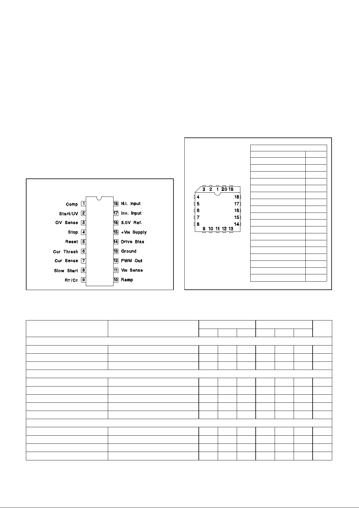
CONNECTION DIAGRAMS
PLCC-20, LCC-20
(TOP VIEW)
Q or L Package
DIL-18, SOIC- 18 (T O P VIEW)
J or N, DW Package
PACKAGE PIN FUNCTIONS
FUNCTION PIN
Comp 1
Start/UV 2
OV Sense 3
Stop 4
Reset 5
CUR Thresh 7
CUR Sense 8
Slow Start 9
R
T/CT 10
Ramp 11
V
IN Sense 12
PWM Out 13
Ground 14
Drive Bias 15
+V
IN Supply 17
5.0V REF 18
Inv. Input 19
N.I. Inpu t 20
ABSOLUTE MAXI MUM RATING S
2
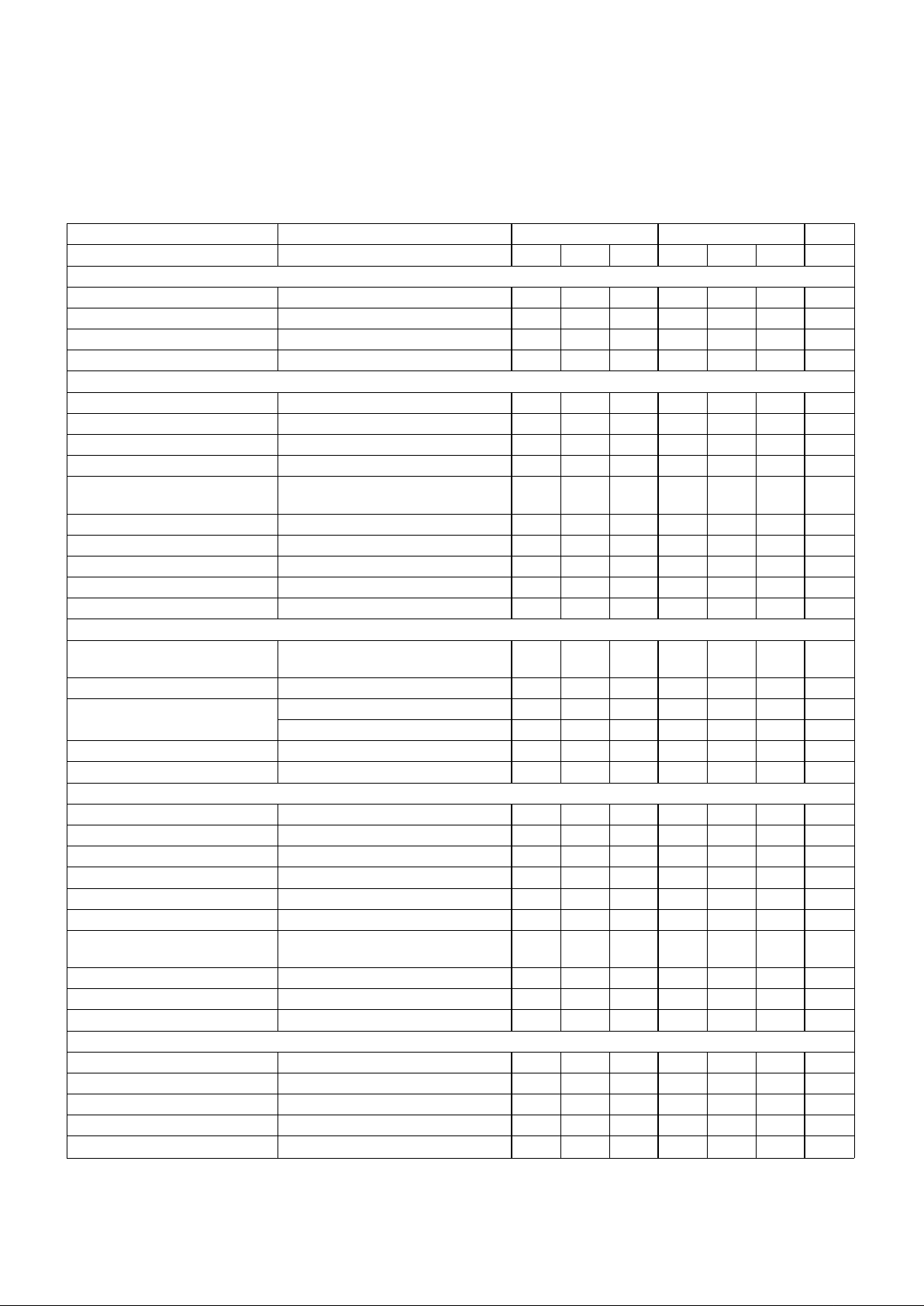
PARAMETER TEST CONDITIONS UC1841 / UC2841 UC3841 UNITS
MIN TYP MAX MIN TYP MAX
Ramp Ge nerator
Ramp Curren t, M in imum I
SENSE = -10µA -11 -14 -11 -14 µA
Ramp Current, Maximum I
SENSE = 1.0mA -0.9 -.95 -0.9 -.95 mA
Ramp Valley 0.3 0.4 0.6 0.3 0.4 0.6 V
Ramp Peak Clamp ing Leve l 3.9 4.2 4.5 3.9 4.2 4.5 V
Error Amplifier
Input Offs et Vo lta g e V
CM = 5.0V 0.5 5 2 10 mV
Input Bias Cur ren t 0.5 2 1 5 µA
Input Offs et Cu rr ent 0.5 0.5 µA
Open Loop Gain ∆V
O= 1 to 3V 60 66 60 66 dB
Output Swing (Max. Output ≤
Ramp Peak - 100mV)
Minimum Total Range 0.3 3.5 0.3 3.5 V
CMRR V
CM = 1.5 to 5.5V 70 80 70 80 dB
PSRR V
IN = 8 to 30V 70 80 70 80 dB
Short Circuit Current V
COMP = 0V -4 -10 -4 -10 mA
Gain Bandwidth* T
J = 25°C, AVOL = 0dB 1 2 1 2 MHz
Slew Rate* T
J = 25°C, AVCL
= 0dB 0.8 0.8 V/µs
PWM Section
Continuous Duty Cycle
Range* (other than zero)
Minimum Total Cont inuou s Range,
Ramp Peak < 4.2V
495495%
50% Duty Cycle Clamp R
SENSE to VREF = 10k 42 47 52 42 47 52 %
Output Saturation I
OUT = 20mA 0.2 0.4 0.2 0.4 V
I
OUT = 200mA 1. 7 2.2 1.7 2.2 V
Output Lea kage V
OUT = 40V 0.1 10 0.1 10 µA
Comparator Dela y* Pin 8 to Pin 12, T
J = 25°C, RL = 1kΩ 300 500 300 500 ns
Sequencing Functions
Comparator Thre sholds P ins 2, 3, 5 2.8 3.0 3.2 2.8 3.0 3.2 V
Input Bias Curren t Pins 3, 5 = 0V -1.0 -4.0 -1.0 -4.0 µA
Input Leakage Pins 3, 5 = 10V 0.1 2.0 0.1 2.0 µA
Start/UV Hyster esis Cur ren t Pin 2 = 2.5V 170 200 220 1 70 200 23 0 µA
Ext. Stop Threshold Pin 4 0.8 1.6 2.4 0.8 1.6 2.4 V
Error Latch Activat e Cur ren t P in 4 = 0V, Pin 3 > 3V -120 -200 -120 -200 µA
Driver Bias Saturation Volta ge,
V
IN - VOH
IB = -50mA 2 3 2 3 V
Driver Bias Leakage V
B = 0V -0.1 -10 -0.1 -10 µA
Slow-Start Saturation I
S = 10mA 0.2 0.5 0.2 0.5 V
Slow-Start Leakage V
S = 4.5V 0.1 2.0 0.1 2.0 µA
Current Control
Current Limit Off set 0 5 0 10 mV
Current Shutdown O ffs et 370 400 430 360 400 440 mV
Input Bias Current Pin 7 = 0V -2 -5 -2 -5 µA
Common Mode Ran ge* -0.4 3.0 -0.4 3.0 V
Current Limit Delay* T
J = 25°C, Pin 7 to 12, RL = 1k 200 400 200 400 n s
* These paramet ers are guara nt eed by design bu t not 100% teste d in prod uct ion.
UC1841
UC2841
UC3841
ELECTRICAL CHARACTERISTICS:
Unless otherwise stated , these spec ificat ions apply for TA = -55°C to +125°C for the
UC1841, -25°C to +85°C for the UC2841, and 0°C to +70 °C for the UC3841; V
IN = 20V, RT = 20k Ω, CT = .001mfd, RR = 10kΩ,
C
R = .001mfd, Current Limit Thresh old = 200mV, TA = TJ.
3

PWM CONTROL
1. Oscillator Gen era tes a fixed-f requency int er nal clock fro m an extern al R
T and CT.
Frequency =
K
C
RTCT
where KC is a first order correction factor ≈ 0.3 log (CT X 1012).
2. Ramp Gener ator
Develops a linear ramp with a slope defined exter nally by
dv
dt
=
sense
voltage
R
RCR
CR is normally se le ct ed ≤ CT and its value will have some effect upon valley voltage.
Limiting the minimum value for I
SENSE will establish a maximum duty cycle clamp.
C
R terminal can be used as an input port for curren t mode cont rol.
3. Error Amplifier Conventional operation al amp lifier f or closed- loop ga in and phase com pe nsat ion.
Low output impedance; unity-gain stable.
The output is held low by the slow star t voltag e at turn on in order to minimize over shoo t.
4. Reference Ge n era tor Precision 5.0V for internal and extern al usage to 50mA.
Tracking 3.0V ref erence for internal usage only w ith nomina l accur acy of
± 2%.
40V clamp zener for chip OV prot ect ion, 100m A maxim um current .
5. PWM Comparat or Gen era tes out put pulse which start s at terminat ion of clock pulse and ends whe n the ramp
input crosses the lowest of two posit iv e input s.
6. PWM Latch Terminat es the PW M output pulse whe n set by inputs fro m either the PWM com pa rator , the
pulse-by-p ulse cur re nt limit com pa rator , or the error la tch. Reset s with each inter nal clock
pulse.
7. PWM Output Switch Transistor cap able of sinking cu rrent to ground which is of f during the PWM on- time and turns
on to terminate the power pulse. Curr ent capacit y is 400m A sat ur ated with peak
capacitance discha rge in excess of one amp.
SEQUENCING FUNCTIONS
1. Start/UV Sense With an increasing vo lta g e, it generat es a turn-on signa l and relea ses t he slow- star t clamp at
a start threshold.
With a decreasing voltage, it gen era tes a turn- off comma nd at a lower leve l separ at ed by a
200
µA hystere sis cur ren t.
2. Drive Switch Disab le s most of the chip to hold inter nal curre nt consump tion low, and Driver Bias OFF, until
input voltage reaches sta rt threshold.
3. Driver Bias Supplies drive current to exter nal power switch to prov ide turn- on bias .
4. Slow Start Clamps low to hold PWM OFF. Upon release, rises with rate contro lled by R
SCS for slow
increase of output pulse widt h.
Can also be used as an alt ernat e m axim um duty cycle clam p with an ext er nal volt age divid er.
PROTECTION FUNCTIO NS
1. Error Latch When set by mome nt ary input , this latch insur es im me diat e PWM shu tdown and hold of f until
reset. Input s t o Err or La tch are :
a. OV > 3.2V (typically 3V)
b. Stop > 2.4V (typically 1.6V)
c. Current Sense 400mV over thr esho ld (typical) .
Error Latch reset s whe n slow start voltage falls to 0.4V if Rese t Pin 5 < 2.8V. Wit h Pin 5 >
3.2V, Error Latch will remain set.
2. Current Lim iti ng Differential input comparator terminat es individual output pulses each t ime sense voltage
rises above thre shold.
When sense volta ge rise s to 400m V (typica l) above th res hold, a shutdo wn signal is sent to
Error Latch.
3. External Stop A voltage over 1.2 V will set the Erro r Latch and hold the ou tp ut off.
A voltage less than 0. 8V wi ll defe a t the erro r lat ch and prev ent shutd o wn.
A capacitor here will slow the action of the erro r latch for tra nsient prot ection by providing a
typical delay of 13ms/
µF.
UC1841
UC2841
UC3841
FUNCTIONAL DES CRIP TIO N
4

UC1841
UC2841
UC3841
Start/UV Hysteresis
PWM Output Minimu m Pu lse W idthOscillator Frequency
PWM Output-Saturation Voltage
Shutdown TimingError Amplifier Op en Loop Gain an d Phase
5

FLYBACK APPLICATION (A)
In this application (see Figure A, next page), complete
control is maintained on the primary side. Control power
is provide d by R
IN and CIN during start-up, and by a pri-
mary-referenced low voltage winding, N2, for efficient operation after start. The error amplifier loop is closed to
regulate the DC voltage from N2 with other outputs following through their magnetic coupling − a task made
even easier with the UC1841’s feed−forward line regula-
tion.
An extension t o this application for more precise regulation would be the use of the UC1901 Isolated Feedback
Generator for direct closed-loop control to an output.
Not shown, are protective snubbers or additional interface
circuitry which may be required by the choice of the highvoltage switch, Qs, or the application; however, one example of power transistor interfacing is provided on the
following page.
REGULATOR APP LI C ATION (B)
With the addition of a level shifting transistor, Q1, the
UC1841 is an ideal control circuit for DC to DC converters
such as the buck regulator shown in Figure B opposite. In
addition t o providin g constant current drive pulses to the
PIC661 power switch, this circuit has full fault protection
and high speed dynamic line regulation due to its feedforward capability. An additional feature is the ability to
UC1841
UC2841
UC3841
OPEN-LOOP TEST CIRCUIT
Nominal Frequency =
1
R
TCT
= 50 kHz
Start Voltage = 3
R1
+ R2 + R3
R2 + R3
+0.2R1 = 12V
UV Fault Volt age = 3
R1
+ R2 + R3
R2 + R3
= 8V
OV Fault V olt age = 3
R1
+ R2 + R3
R3
= 32V
Current Limit = 200mV
Current Fault Voltage = 600mV
Duty Cycle Clamp = 50%
6

UC1841
UC2841
UC3841
Figure A. UC1841 Programma ble PW M Cont roller In A Simplified Flyback Regulator
Figure B. Overall Schematic For A 300 Watt, Off -line Power Converter Using The UC 3 841 For Control
7

Since Pin 10 is a direct input to the PWM comparator, this
point can also serve as a current sense port for current mode
control. In this application, current sensing is ground referenced through R
CS. Resistor R1 sets a 400mV offset across
R2 (assuming R2 > R
CS) so that both the Error Amplifier and
Fault Shutdown can force the current complete ly to zero. R2 is
also used along with C
F as a small filter to attenuate leading-
edge spikes on the load current waveform. In this mode,
current limiting can be accomplished by divider R3/R4 which
forms a clamp o ver riding the out put of t he Er ror Am plifier.
In this circuit, R1 is used in conjunction with C
R (not shown) to
establish a minimum ramp charging current such that the ramp
voltage reaches 4.2V at the required maximum output pulse
width.
The purpose of Q1 is to provide an increasing ramp current
above a threshold established by R2 and R3 such that the d ut y
cycle is further reduc ed with increa sing VIN.
The minimum ramp current is:
l
R(MIN) =
V
REF − VIN SENSE
R1
≈
4
V
R1
The threshold where VIN begins to add extra ramp curren t is:
V
IN ≈ 5.6V
R2 + R3R3
Above the threshold, the ramp curr ent will be:
l
R (VARIAB ) ≈
4
R1
+
VIN − 5.6
R2
−
5.6
R3
UC1841
UC2841
UC3841
ERROR LATCH INTERNAL CIRCUITRY
PROGRAMMABLE SOFT START AND
RESTART DELAY CIRCUIT
The Error Latch consists of Q5 and Q6 which, when both on,
turns off the PWM Output and pulls the Slow-Start pin low . This
latch is set by either the Over-Voltage or Current Shutdown
comparators, or by a high signal on Pin 4. Reset is accomplished by either the Reset comparator or a low signal on Pin
4. An activation time delay can be provided with an external
capacitor on Pin 4 in conjunction with the ≈ 100µA collector
current from Q4.
UNITRODE INTEGRATED CIRCUITS
7 CONTINENTAL BLVD. • MERRIMACK, NH 03054
TEL. (603) 424-2410 • FAX (603) 424-3460
VOLTAGE FEED-FO RWARD COMBINED WITH
MAXIMUM DUTY-CYCLE CLAMP
CURRENT MODE CONTROL
8

IMPORTANT NOTICE
T exas Instruments and its subsidiaries (TI) reserve the right to make changes to their products or to discontinue
any product or service without notice, and advise customers to obtain the latest version of relevant information
to verify, before placing orders, that information being relied on is current and complete. All products are sold
subject to the terms and conditions of sale supplied at the time of order acknowledgement, including those
pertaining to warranty, patent infringement, and limitation of liability.
TI warrants performance of its semiconductor products to the specifications applicable at the time of sale in
accordance with TI’s standard warranty. Testing and other quality control techniques are utilized to the extent
TI deems necessary to support this warranty. Specific testing of all parameters of each device is not necessarily
performed, except those mandated by government requirements.
CERT AIN APPLICATIONS USING SEMICONDUCTOR PRODUCTS MAY INVOLVE POTENTIAL RISKS OF
DEATH, PERSONAL INJURY, OR SEVERE PROPERTY OR ENVIRONMENTAL DAMAGE (“CRITICAL
APPLICATIONS”). TI SEMICONDUCTOR PRODUCTS ARE NOT DESIGNED, AUTHORIZED, OR
WARRANTED TO BE SUITABLE FOR USE IN LIFE-SUPPORT DEVICES OR SYSTEMS OR OTHER
CRITICAL APPLICATIONS. INCLUSION OF TI PRODUCTS IN SUCH APPLICA TIONS IS UNDERSTOOD T O
BE FULLY AT THE CUSTOMER’S RISK.
In order to minimize risks associated with the customer’s applications, adequate design and operating
safeguards must be provided by the customer to minimize inherent or procedural hazards.
TI assumes no liability for applications assistance or customer product design. TI does not warrant or represent
that any license, either express or implied, is granted under any patent right, copyright, mask work right, or other
intellectual property right of TI covering or relating to any combination, machine, or process in which such
semiconductor products or services might be or are used. TI’s publication of information regarding any third
party’s products or services does not constitute TI’s approval, warranty or endorsement thereof.
Copyright 1999, Texas Instruments Incorporated
 Loading...