

1 2
3
4
5
6
7
8
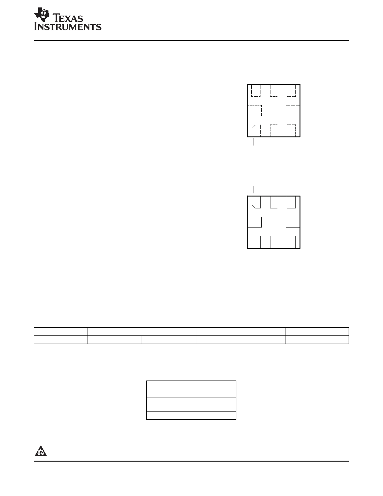
HSD–
HSD+
OE
D
–
D+
N.C.
GND
V
CC
RSEPACKAGE
(TOP VIEW)
1 2
3
4
5
6
7
8
RSEPACKAGE
(BOTTOMVIEW)
HSD+
N.C.
D+
D–
OE
GND
V
CC
HSD–
N.C. Nointernalconnection-
www.ti.com
1
FEATURES
• V
Operation at 3 V and 4.3 V
CC
• 1.8-V Compatible Control-Pin Inputs
• I
Supports Partial Power-Down Mode
OFF
Operation
• ron= 10 Ω Maximum
• Δ ron<0.35 Ω Typical
• C
= 6 pF Typical
io(ON)
• Low Power Consumption (1 µ A Maximum)
• ESD Performance Tested Per JESD 22
– 6000-V Human-Body Model
(A114-B, Class II)
– 1000-V Charged-Device Model (C101)
– 250-V Machine Model (A115-A)
• Wide – 3-dB Bandwidth = 1220 MHz Typical
• Packaged in 8-Pin TQFN (1.5 mm × 1.5 mm)
TS3USB31
HIGH-SPEED USB 2.0 (480-Mbps) 1-PORT SWITCH
WITH SINGLE ENABLE
SCDS242D – JULY 2007 – REVISED JANUARY 2008
APPLICATIONS
• Routes Signals for USB 1.0, 1.1, and 2.0
DESCRIPTION/ORDERING INFORMATION
The TS3USB31 is a high-bandwidth switch specially
designed for the switching of high-speed USB 2.0
signals in handset and consumer applications, such
as cell phones, digital cameras, and notebooks with
hubs or controllers with limited USB I/Os. The wide
bandwidth (750 MHz) of this switch allows signals to
pass with minimum edge and phase distortion. The
switch is bidirectional and offers little or no
attenuation of the high-speed signals at the outputs. It
is designed for low bit-to-bit skew and high
channel-to-channel noise isolation, and is compatible
with various standards, such as high-speed USB 2.0
(480 Mbps).
– 40 ° C to 85 ° C QFN – RSE Tape and reel TS3USB31RSER L9
(1) Package drawings, thermal data, and symbolization are available at www.ti.com/packaging .
(2) For the most current package and ordering information, see the Package Option Addendum at the end of this document, or see the TI
T
A
website at www.ti.com .
ORDERING INFORMATION
PACKAGE
(1) (2)
ORDERABLE PART NUMBER TOP-SIDE MARKING
PIN DESCRIPTION
NAME DESCRIPTION
OE Bus-switch enable
D+, D – ,
HSD+, HSD –
NC No connect
Data ports
1
PRODUCTION DATA information is current as of publication date.
Products conform to specifications per the terms of the Texas
Instruments standard warranty. Production processing does not
necessarily include testing of all parameters.
Please be aware that an important notice concerning availability, standard warranty, and use in critical applications of
Texas Instruments semiconductor products and disclaimers thereto appears at the end of this data sheet.
Copyright © 2007 – 2008, Texas Instruments Incorporated
www.ti.com
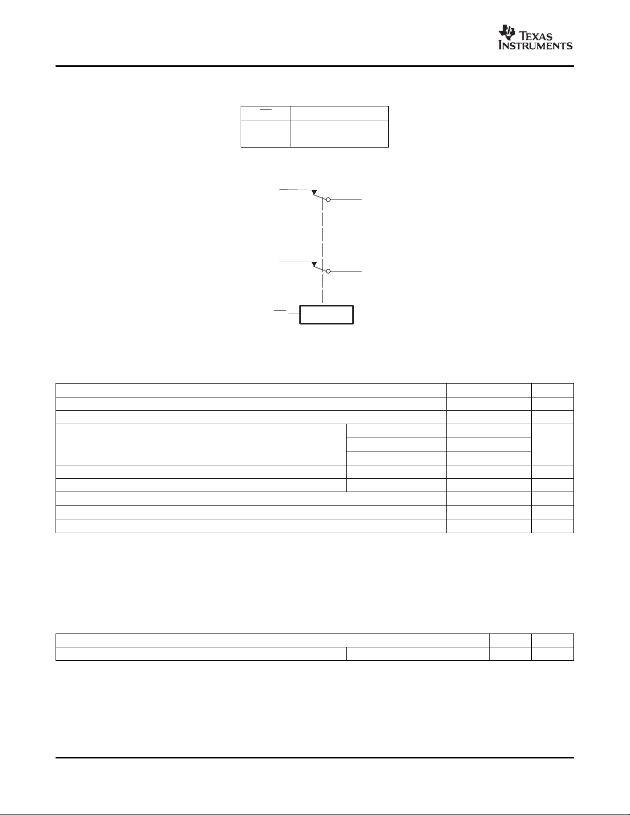
HSD1+
HSD1–
Control
D+
D–
OE
TS3USB31
HIGH-SPEED USB 2.0 (480-Mbps) 1-PORT SWITCH
WITH SINGLE ENABLE
SCDS242D – JULY 2007 – REVISED JANUARY 2008
TRUTH TABLE
OE FUNCTION
H Disconnect
L D+, D – = HSD+, HSD –
BLOCK DIAGRAM
ABSOLUTE MAXIMUM RATINGS
(1)
over operating free-air temperature range (unless otherwise noted)
MIN MAX UNIT
V
CC
V
IN
V
I/O
I
IK
I
I/OK
I
I/O
T
stg
Supply voltage range – 0.5 7 V
(2) (3) (4)
(2) (3)
HSD+, HSD – – 0.5 V
D+, D – when V
D+, D – when V
> 0 – 0.5 V
CC
= 0 5.25
CC
– 0.5 7 V
+ 0.3
CC
+ 0.3 V
CC
Control input voltage range
Switch I/O voltage range
Control input clamp current VIN< 0 – 50 mA
I/O port clamp current V
ON-state switch current
Continuous current through V
(5)
or GND ± 100 mA
CC
< 0 – 50 mA
I/O
Storage temperature range – 65 150 ° C
(1) Stresses beyond those listed under "absolute maximum ratings" may cause permanent damage to the device. These are stress ratings
only, and functional operation of the device at these or any other conditions beyond those indicated under "recommended operating
conditions" is not implied. Exposure to absolute-maximum-rated conditions for extended periods may affect device reliability.
(2) All voltages are with respect to ground, unless otherwise specified.
(3) The input and output voltage ratings may be exceeded if the input and output clamp-current ratings are observed.
(4) VIand VOare used to denote specific conditions for V
(5) IIand IOare used to denote specific conditions for I
.
I/O
.
I/O
PACKAGE THERMAL IMPEDANCE
θ
JA
Package thermal impedance
(1) The package thermal impedance is calculated in accordance with JESD 51-7.
(1)
RSE package 253 ° C/W
± 64 mA
TYP UNIT
2 Submit Documentation Feedback Copyright © 2007 – 2008, Texas Instruments Incorporated
Product Folder Link(s): TS3USB31
www.ti.com
HIGH-SPEED USB 2.0 (480-Mbps) 1-PORT SWITCH
WITH SINGLE ENABLE
SCDS242D – JULY 2007 – REVISED JANUARY 2008
TS3USB31
RECOMMENDED OPERATING CONDITIONS
(1)
MIN MAX UNIT
V
V
V
V
T
(1) All unused control inputs of the device must be held at V
ELECTRICAL CHARACTERISTICS
Supply voltage 3.0 4.3 V
CC
V
= 3 V to 3.6 V 1.3
High-level control input voltage V
IH
Low-level control input voltage V
IL
Data input/output voltage 0 V
I/O
Operating free-air temperature – 40 85 ° C
A
Implications of Slow or Floating CMOS Inputs, literature number SCBA004.
(1)
CC
CC
V
= 4.3 V 1.7
CC
V
= 3 V to 3.6 V 0.5
CC
V
= 4.3 V 0.7
CC
or GND to ensure proper device operation. Refer to the TI application report,
CC
over operating free-air temperature range (unless otherwise noted)
PARAMETER TEST CONDITIONS MIN TYP
V
IK
I
IN
I
OZ
I
OFF
I
CC
Δ I
C
C
C
r
on
Δ r
r
on(flat)
(3)
(4)
CC
in
io(OFF)
io(ON)
(5)
on
Control inputs V
D+ and D – V
Control inputs V
Control inputs V
V
= 3 V, II= – 18 mA – 1.2 V
CC
= 4.3 V, VIN= 0 to 4.3 V, V
CC
V
= 4.3 V, VO= 0 to 3.6 V, VI= 0, Switch OFF ± 1 µ A
CC
= 0 V, VO= 0 to 4.3 V, VI= 0, VIN= V
CC
V
= 4.3 V, I
CC
= 4.3 V, VIN= 2.6 V 10 µ A
CC
= 0 V, VIN= V
CC
V
= 3.3 V, V
CC
V
= 3.3 V, V
CC
V
= 3 V, VI= 0.4 V, IO= – 8 mA 6 10 Ω
CC
V
= 3 V, VI= 0.4 V, IO= – 8 mA 0.35 Ω
CC
V
= 3 V, VI= 0 V or 1 V, IO= – 8 mA 2 Ω
CC
= 0, Switch ON or OFF 1 µ A
I/O
or GND 1 pF
CC
= 3.3 V or 0, Switch OFF 2 pF
I/O
= 3.3 V or 0, Switch ON 6 pF
I/O
= 0 V ± 1 µ A
CC
or GND ± 2 µ A
CC
(1) VINand IINrefer to control inputs. VI, VO, II, and IOrefer to data pins.
(2) All typical values are at V
(3) For I/O ports, the parameter IOZincludes the input leakage current.
= 3.3 V (unless otherwise noted), TA= 25 ° C.
CC
(4) This is the increase in supply current for each input that is at the specified TTL voltage level, rather than V
(5) Measured by the voltage drop between the A and B terminals at the indicated current through the switch. ON-state resistance is
determined by the lower of the voltages of the two (A or B) terminals.
(2)
MAX UNIT
or GND.
CC
V
DYNAMIC ELECTRICAL CHARACTERISTICS
over operating range, TA= – 40 ° C to 85 ° C, V
PARAMETER TEST CONDITIONS TYP
X
TALK
O
IRR
BW Bandwidth ( – 3 dB) RL= 50 Ω , CL= 5 pF, See Figure 10 1220 MHz
(1) For Max or Min conditions, use the appropriate value specified under Electrical Characteristics for the applicable device type.
Copyright © 2007 – 2008, Texas Instruments Incorporated Submit Documentation Feedback 3
Crosstalk RL= 50 Ω , f = 240 MHz, See Figure 9 – 53 dB
OFF isolation RL= 50 Ω , f = 240 MHz, See Figure 8 – 30 dB
= 3.3 V ± 10%, GND = 0 V
CC
Product Folder Link(s): TS3USB31
(1)
UNIT
www.ti.com
TS3USB31
HIGH-SPEED USB 2.0 (480-Mbps) 1-PORT SWITCH
WITH SINGLE ENABLE
SCDS242D – JULY 2007 – REVISED JANUARY 2008
SWITCHING CHARACTERISTICS
over operating range, TA= – 40 ° C to 85 ° C, V
PARAMETER TEST CONDITIONS MIN TYP
t
t
t
t
t
t
Propagation delay
pd
Line enable time, OE to D, nD 30 ns
ON
Line disable time, OE to D, nD 25 ns
OFF
Output skew between center port to any other port
SK(O)
Skew between opposite transitions of the same output RL= 50 Ω , CL= 5 pF,
SK(P)
(t
– t
PHL
PLH
Total jitter
J
(1) For Max or Min conditions, use the appropriate value specified under Electrical Characteristics for the applicable device type.
(2) Specified by design
(3) The bus switch contributes no propagational delay other than the RC delay of the on resistance of the switch and the load capacitance.
The time constant for the switch alone is of the order of 0.25 ns for 10-pF load. Since this time constant is much smaller than the rise/fall
times of typical driving signals, it adds very little propagational delay to the system. Propagational delay of the bus switch, when used in
a system, is determined by the driving circuit on the driving side of the switch and its interactions with the load on the driven side.
(2) (3)
(2)
)
(2)
= 3.3 V ± 10%, GND = 0 V
CC
RL= 50 Ω , CL= 5 pF,
See Figure 11
RL= 50 Ω , CL= 5 pF,
See Figure 7
RL= 50 Ω , CL= 5 pF,
See Figure 7
(2)
RL= 50 Ω , CL= 5 pF,
See Figure 12
See Figure 12
RL= 50 Ω , CL= 5 pF,
tR= tF= 500 ps at 480 Mbps 200 ps
(PRBS = 215– 1)
(1)
0.25 ns
50 ps
20 ps
MAX UNIT
4 Submit Documentation Feedback Copyright © 2007 – 2008, Texas Instruments Incorporated
Product Folder Link(s): TS3USB31
www.ti.com
–90
–80
–70
–60
–50
–40
–30
–20
–10
0
100.0E+3 1.0E+6 10.0E+6 100.0E+6 1.0E+9 10.0E+9
Frequency(Hz)
Attenuation(dB)
-8
-7
-6
-5
-4
-3
-2
-1
0
1.0E+06 1.0E+07 1.0E+08 1.0E+09 1.0E+10
Frequency(Hz)
Magnitude (dB)
–100
–120
–80
–60
–40
–20
0
100.0E+3 1.0E+6 10.0E+6 100.0E+6 1.0E+9 10.0E+9
Frequency (Hz)
Attenuation (dB)
TS3USB31
V
CC
USB
Connector
Base Band
Processor
or FS USB
Controller
HS USB
Controller
HIGH-SPEED USB 2.0 (480-Mbps) 1-PORT SWITCH
SCDS242D – JULY 2007 – REVISED JANUARY 2008
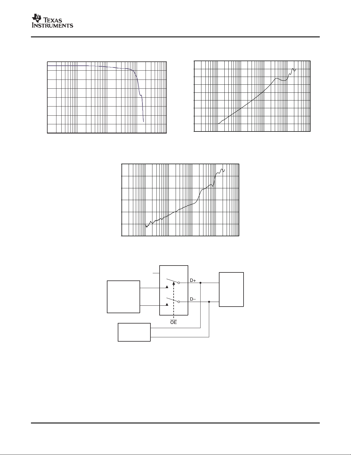
APPLICATION INFORMATION
Figure 1. Insertion Loss Figure 2. OFF Isolation
TS3USB31
WITH SINGLE ENABLE
Copyright © 2007 – 2008, Texas Instruments Incorporated Submit Documentation Feedback 5
Figure 3. Crosstalk
Figure 4. Application Diagram
Product Folder Link(s): TS3USB31
www.ti.com
Time ( 10 ) (s)X
–9
Differential Signal (V)
0.0
–0.5
0.5
–0.4
0.4
–0.3
0.3
–0.2
0.2
–0.1
0.1
0.0
0.2 0.4 0.5 0.8 1.0 1.2 1.4 1.6 1.8 2.0
Time ( 10 ) (s)X
–9
Differential Signal (V)
0.0
–0.5
0.5
–0.4
0.4
–0.3
0.3
–0.2
0.2
–0.1
0.1
0.0
0.2 0.4 0.5 0.8 1.0 1.2 1.4 1.6 1.8 2.0
TS3USB31
HIGH-SPEED USB 2.0 (480-Mbps) 1-PORT SWITCH
WITH SINGLE ENABLE
SCDS242D – JULY 2007 – REVISED JANUARY 2008
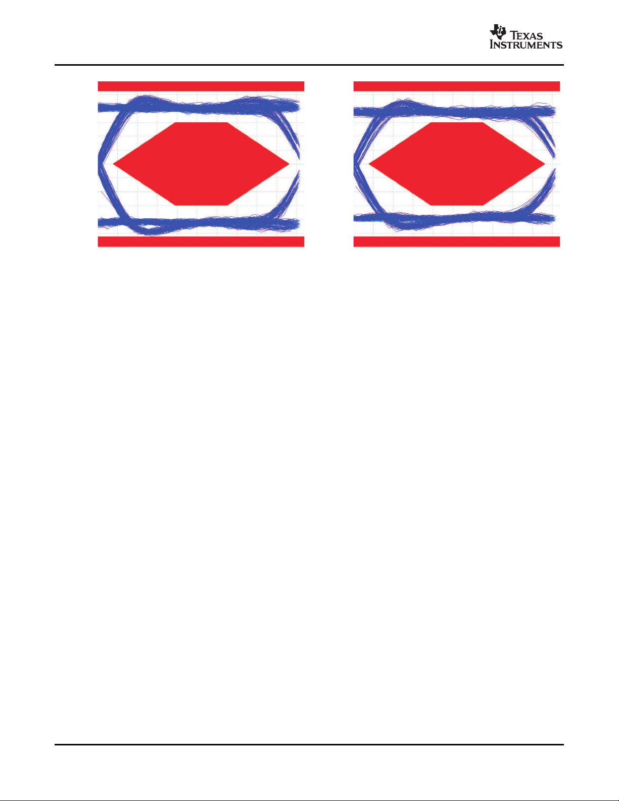
Figure 5. Eye Pattern: 480-Mbps USB Signal With No Figure 6. Eye Pattern: 480-Mbps USB Signal With Switch
Switch (Through Path) NO Path
6 Submit Documentation Feedback Copyright © 2007 – 2008, Texas Instruments Incorporated
Product Folder Link(s): TS3USB31
www.ti.com
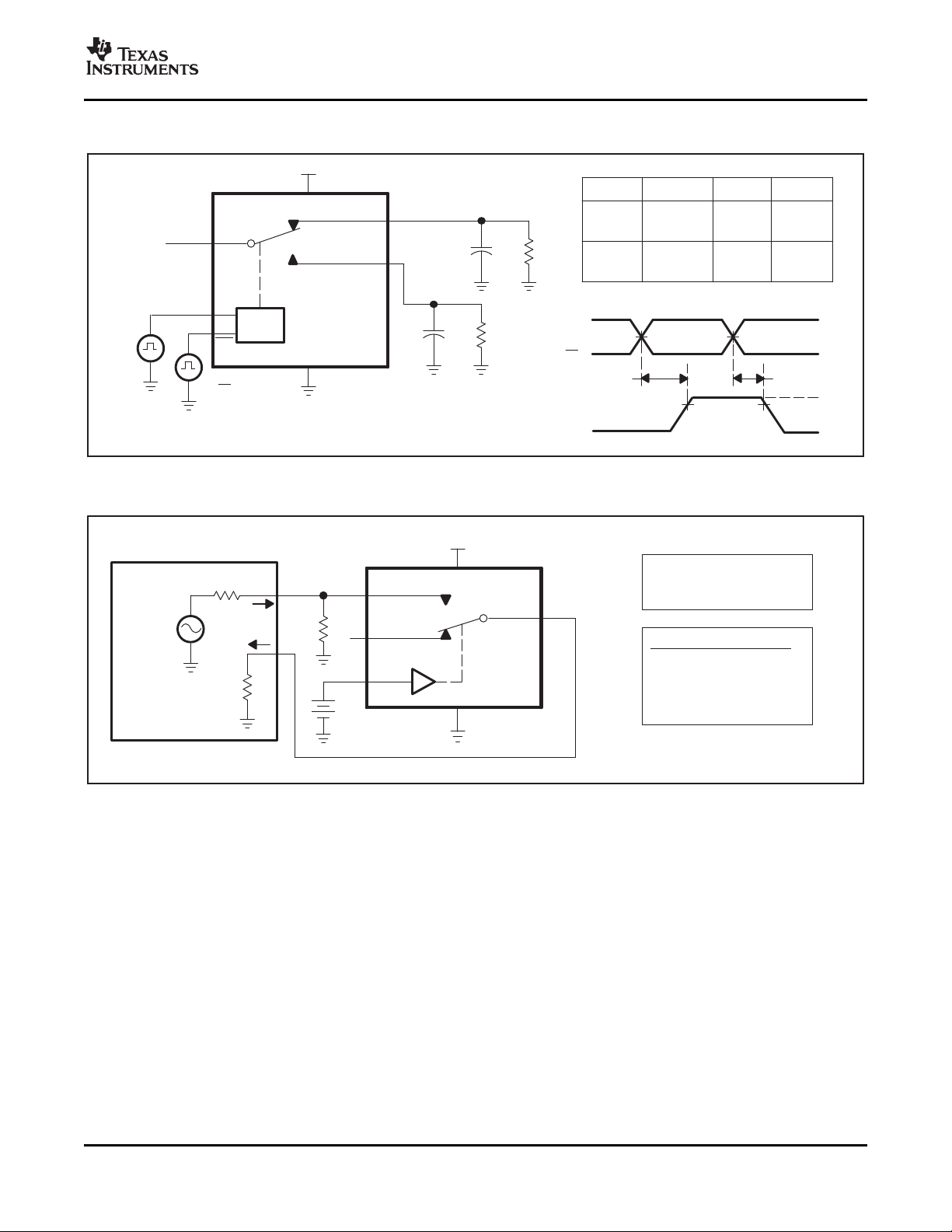
PARAMETER MEASUREMENT INFORMATION
C
L
(B)
R
L
V
IN
V
CC
GND
1Dor2D
V
OUT1
1Dor2D
D
V
CC
V
IN
50 Ω
R
L
C
L
5pFt
ON
TEST
V
CC
50 Ω 5pFt
OFF
50%
t
ON
t
OFF
50%
90% 90%
Logic
Input
(V
SEL
or VOE)
1.8 V
Switch
Output
(V
OUT1
or V
OUT2
)
0
C
L
(B)
R
L
V
OH
V
OL
OE
V
OUT2
V
OE
(A)
V
SEL
(A)
S
1D
2D
D
V
OUT1
V
IN
Channel OFF: 1D to D
Network Analyzer Setup
Source Power = 0 dBm
(632-mV P-P at 50-W load)
DC Bias = 350 mV
50 W
V
CC
GND
50 W
50 W
Network Analyzer
Source
Signal
V
SEL
+
V
SEL
= V
CC
S
TS3USB31
HIGH-SPEED USB 2.0 (480-Mbps) 1-PORT SWITCH
WITH SINGLE ENABLE
SCDS242D – JULY 2007 – REVISED JANUARY 2008
Figure 7. Turn-On (t
Figure 8. OFF Isolation (O
) and Turn-Off Time (t
ON
)
OFF
)
IRR
Copyright © 2007 – 2008, Texas Instruments Incorporated Submit Documentation Feedback 7
Product Folder Link(s): TS3USB31

www.ti.com
1D
2D
50 W
50 W
V
OUT1
V
IN
Channel ON: 1D to D
Network Analyzer Setup
Source Power = 0 dBm
(632-mV P-P at 50-W load)
DC Bias = 350 mV
50 W
V
CC
GND
V
OUT2
Source
Signal
Channel OFF: 2D to D
Network Analyzer
V
SEL
+
V
SEL
= V
CC
S
V
CC
GND
1D
V
SEL
2D
D
50 W
50 W
V
OUT1
V
IN
Channel ON: 1D to D
Network Analyzer Setup
Source Power = 0 dBm
(632-mV P-P at 50-W load)
DC Bias = 350 mV
Network Analyzer
Source
Signal
V
CTRL
= GND
S
GND
400 mV
TS3USB31
HIGH-SPEED USB 2.0 (480-Mbps) 1-PORT SWITCH
WITH SINGLE ENABLE
SCDS242D – JULY 2007 – REVISED JANUARY 2008
PARAMETER MEASUREMENT INFORMATION (continued)
Figure 9. Crosstalk (X
Figure 10. Bandwidth (BW)
)
TALK
8 Submit Documentation Feedback Copyright © 2007 – 2008, Texas Instruments Incorporated
Figure 11. Propagation Delay
Product Folder Link(s): TS3USB31

www.ti.com
Pulse Skew t
SK(P)
Output Skew t
SK(P)
V
OL
V
OH
V
OH
V
OL
V
OH
V
OL
HIGH-SPEED USB 2.0 (480-Mbps) 1-PORT SWITCH
PARAMETER MEASUREMENT INFORMATION (continued)
TS3USB31
WITH SINGLE ENABLE
SCDS242D – JULY 2007 – REVISED JANUARY 2008
Figure 12. Skew Test
Copyright © 2007 – 2008, Texas Instruments Incorporated Submit Documentation Feedback 9
Product Folder Link(s): TS3USB31

www.ti.com
V
CC
I
IN
r
on
+
VIN* V
OUT2
or V
OUT1
I
IN
W
GND
Channel ON
1D
V
SEL
2D
D
V
IN
V
SEL
= V
IH
or V
IL
V
OUT2
V
OUT1
+
+
S
Channel OFF
OFF-State Leakage Current
V
SEL
= V
IH
or V
IL
V
CC
GND
1D
V
SEL
2D
D
V
IN
V
OUT2
V
OUT1
+
+
+
S
V
CC
GND
V
BIAS
V
SEL
V
SEL
= VCC or GND
V
BIAS
= VCC or GND
Capacitance is measured at 1D,
2D, D, and S inputs during ON
and OFF conditions.
Capacitance
Meter
V
IN
V
OUT2
V
OUT1
D
2D
1D
S
TS3USB31
HIGH-SPEED USB 2.0 (480-Mbps) 1-PORT SWITCH
WITH SINGLE ENABLE
SCDS242D – JULY 2007 – REVISED JANUARY 2008
PARAMETER MEASUREMENT INFORMATION (continued)
Figure 13. ON-State Resistance (r
Figure 14. OFF-State Leakage Current
)
on
10 Submit Documentation Feedback Copyright © 2007 – 2008, Texas Instruments Incorporated
Figure 15. Capacitance
Product Folder Link(s): TS3USB31

PACKAGE OPTION ADDENDUM
www.ti.com
17-Jan-2008
PACKAGING INFORMATION
Orderable Device Status
(1)
Package
Type
Package
Drawing
Pins Package
Qty
Eco Plan
TS3USB31RSER ACTIVE QFN RSE 8 3000 Green (RoHS &
no Sb/Br)
TS3USB31RSERG4 ACTIVE QFN RSE 8 3000 Green (RoHS &
no Sb/Br)
(1)
The marketing status values are defined as follows:
ACTIVE: Product device recommended for new designs.
LIFEBUY: TI has announced that the device will be discontinued, and a lifetime-buy period is in effect.
NRND: Not recommended for new designs. Device is in production to support existing customers, but TI does not recommend using this part in
a new design.
PREVIEW: Device has been announced but is not in production. Samples may or may not be available.
OBSOLETE: TI has discontinued the production of the device.
(2)
Eco Plan - The planned eco-friendly classification: Pb-Free (RoHS), Pb-Free (RoHS Exempt), or Green (RoHS & no Sb/Br) - please check
http://www.ti.com/productcontent for the latest availability information and additional product content details.
TBD: The Pb-Free/Green conversion plan has not been defined.
Pb-Free (RoHS): TI's terms "Lead-Free" or "Pb-Free" mean semiconductor products that are compatible with the current RoHS requirements
for all 6 substances, including the requirement that lead not exceed 0.1% by weight in homogeneous materials. Where designed to be soldered
at high temperatures, TI Pb-Free products are suitable for use in specified lead-free processes.
Pb-Free (RoHS Exempt): This component has a RoHS exemption for either 1) lead-based flip-chip solder bumps used between the die and
package, or 2) lead-based die adhesive used between the die and leadframe. The component is otherwise considered Pb-Free (RoHS
compatible) as defined above.
Green (RoHS & no Sb/Br): TI defines "Green" to mean Pb-Free (RoHS compatible), and free of Bromine (Br) and Antimony (Sb) based flame
retardants (Br or Sb do not exceed 0.1% by weight in homogeneous material)
(2)
Lead/Ball Finish MSL Peak Temp
CU NIPDAU Level-1-260C-UNLIM
CU NIPDAU Level-1-260C-UNLIM
(3)
(3)
MSL, Peak Temp. -- The Moisture Sensitivity Level rating according to the JEDEC industry standard classifications, and peak solder
temperature.
Important Information and Disclaimer:The information provided on this page represents TI's knowledge and belief as of the date that it is
provided. TI bases its knowledge and belief on information provided by third parties, and makes no representation or warranty as to the
accuracy of such information. Efforts are underway to better integrate information from third parties. TI has taken and continues to take
reasonable steps to provide representative and accurate information but may not have conducted destructive testing or chemical analysis on
incoming materials and chemicals. TI and TI suppliers consider certain information to be proprietary, and thus CAS numbers and other limited
information may not be available for release.
In no event shall TI's liability arising out of such information exceed the total purchase price of the TI part(s) at issue in this document sold by TI
to Customer on an annual basis.
Addendum-Page 1

PACKAGE MATERIALS INFORMATION
www.ti.com
TAPE AND REEL INFORMATION
11-Mar-2008
*All dimensions are nominal
Device Package
Type
TS3USB31RSER QFN RSE 8 3000 179.0 8.4 1.7 1.7 0.76 4.0 8.0 Q2
Package
Drawing
Pins SPQ Reel
Diameter
(mm)
Reel
Width
W1 (mm)
A0 (mm) B0 (mm) K0 (mm) P1
(mm)W(mm)
Pin1
Quadrant
Pack Materials-Page 1

PACKAGE MATERIALS INFORMATION
www.ti.com
11-Mar-2008
*All dimensions are nominal
Device Package Type Package Drawing Pins SPQ Length (mm) Width (mm) Height (mm)
TS3USB31RSER QFN RSE 8 3000 220.0 205.0 50.0
Pack Materials-Page 2


IMPORTANT NOTICE
Texas Instruments Incorporated and its subsidiaries (TI) reserve the right to make corrections, modifications, enhancements, improvements,
and other changes to its products and services at any time and to discontinue any product or service without notice. Customers should
obtain the latest relevant information before placing orders and should verify that such information is current and complete. All products are
sold subject to TI’s terms and conditions of sale supplied at the time of order acknowledgment.
TI warrants performance of its hardware products to the specifications applicable at the time of sale in accordance with TI’s standard
warranty. Testing and other quality control techniques are used to the extent TI deems necessary to support this warranty. Except where
mandated by government requirements, testing of all parameters of each product is not necessarily performed.
TI assumes no liability for applications assistance or customer product design. Customers are responsible for their products and
applications using TI components. To minimize the risks associated with customer products and applications, customers should provide
adequate design and operating safeguards.
TI does not warrant or represent that any license, either express or implied, is granted under any TI patent right, copyright, mask work right,
or other TI intellectual property right relating to any combination, machine, or process in which TI products or services are used. Information
published by TI regarding third-party products or services does not constitute a license from TI to use such products or services or a
warranty or endorsement thereof. Use of such information may require a license from a third party under the patents or other intellectual
property of the third party, or a license from TI under the patents or other intellectual property of TI.
Reproduction of TI information in TI data books or data sheets is permissible only if reproduction is without alteration and is accompanied
by all associated warranties, conditions, limitations, and notices. Reproduction of this information with alteration is an unfair and deceptive
business practice. TI is not responsible or liable for such altered documentation. Information of third parties may be subject to additional
restrictions.
Resale of TI products or services with statements different from or beyond the parameters stated by TI for that product or service voids all
express and any implied warranties for the associated TI product or service and is an unfair and deceptive business practice. TI is not
responsible or liable for any such statements.
TI products are not authorized for use in safety-critical applications (such as life support) where a failure of the TI product would reasonably
be expected to cause severe personal injury or death, unless officers of the parties have executed an agreement specifically governing
such use. Buyers represent that they have all necessary expertise in the safety and regulatory ramifications of their applications, and
acknowledge and agree that they are solely responsible for all legal, regulatory and safety-related requirements concerning their products
and any use of TI products in such safety-critical applications, notwithstanding any applications-related information or support that may be
provided by TI. Further, Buyers must fully indemnify TI and its representatives against any damages arising out of the use of TI products in
such safety-critical applications.
TI products are neither designed nor intended for use in military/aerospace applications or environments unless the TI products are
specifically designated by TI as military-grade or "enhanced plastic." Only products designated by TI as military-grade meet military
specifications. Buyers acknowledge and agree that any such use of TI products which TI has not designated as military-grade is solely at
the Buyer's risk, and that they are solely responsible for compliance with all legal and regulatory requirements in connection with such use.
TI products are neither designed nor intended for use in automotive applications or environments unless the specific TI products are
designated by TI as compliant with ISO/TS 16949 requirements. Buyers acknowledge and agree that, if they use any non-designated
products in automotive applications, TI will not be responsible for any failure to meet such requirements.
Following are URLs where you can obtain information on other Texas Instruments products and application solutions:
Products Applications
Amplifiers amplifier.ti.com Audio www.ti.com/audio
Data Converters dataconverter.ti.com Automotive www.ti.com/automotive
DSP dsp.ti.com Broadband www.ti.com/broadband
Clocks and Timers www.ti.com/clocks Digital Control www.ti.com/digitalcontrol
Interface interface.ti.com Medical www.ti.com/medical
Logic logic.ti.com Military www.ti.com/military
Power Mgmt power.ti.com Optical Networking www.ti.com/opticalnetwork
Microcontrollers microcontroller.ti.com Security www.ti.com/security
RFID www.ti-rfid.com Telephony www.ti.com/telephony
RF/IF and ZigBee® Solutions www.ti.com/lprf Video & Imaging www.ti.com/video
Mailing Address: Texas Instruments, Post Office Box 655303, Dallas, Texas 75265
Copyright © 2008, Texas Instruments Incorporated
Wireless www.ti.com/wireless
 Loading...