

Page 1
www.ti.com
J
H
G
F
E
D
C
B
A
8
2
3 4 5 6
5mm
9
1
7
5 mm
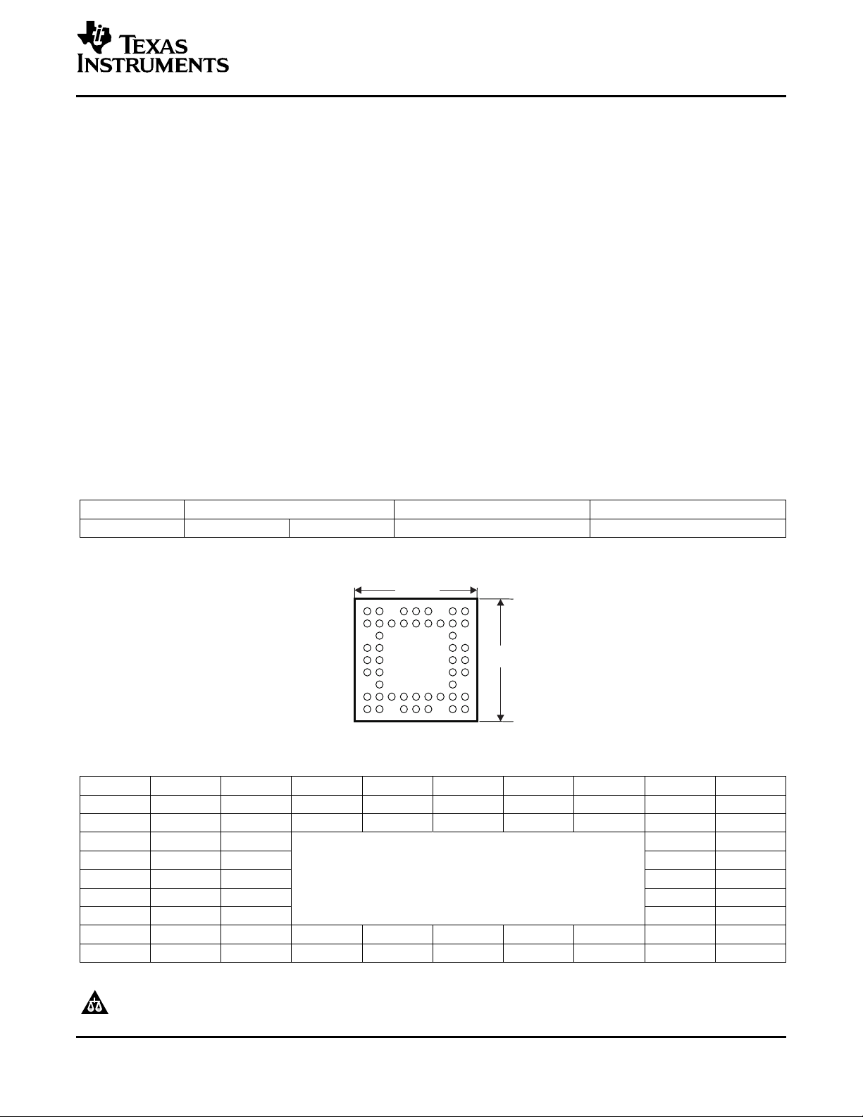
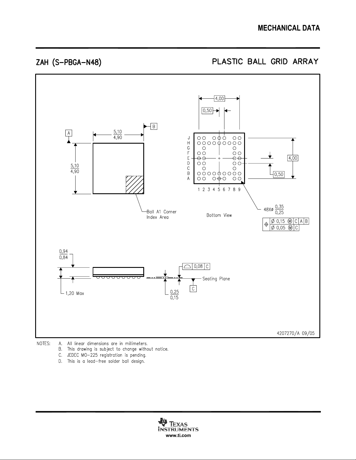
ZAHPACKAGE
(BOTTOMVIEW)
TS2PCIE2212
PCI Express™ SIGNAL SWITCH
SCDS209 – JUNE 2006
FEATURES
• Offers Bandwidth Allocation of PCI Express™ • Excellent Differential Skew (5 ps Max)
Signal Using Two-Lane 1:2
Multiplexer/Demultiplexer
• Vcc Operating Range From 1.7 V to 1.9 V
• Supports Data Rates of 2.5 Gbps
• Port-Port Crosstalk (–39 dB at 1.25 GHz)
• OFF Port Isolation (–38 dB at 1.25 GHz)
• Low ON-State Resistance (10 Ω Typ)
• Low Input/Output Capacitance (3.5 pF Typ)
DESCRIPTION/ORDERING INFORMATION
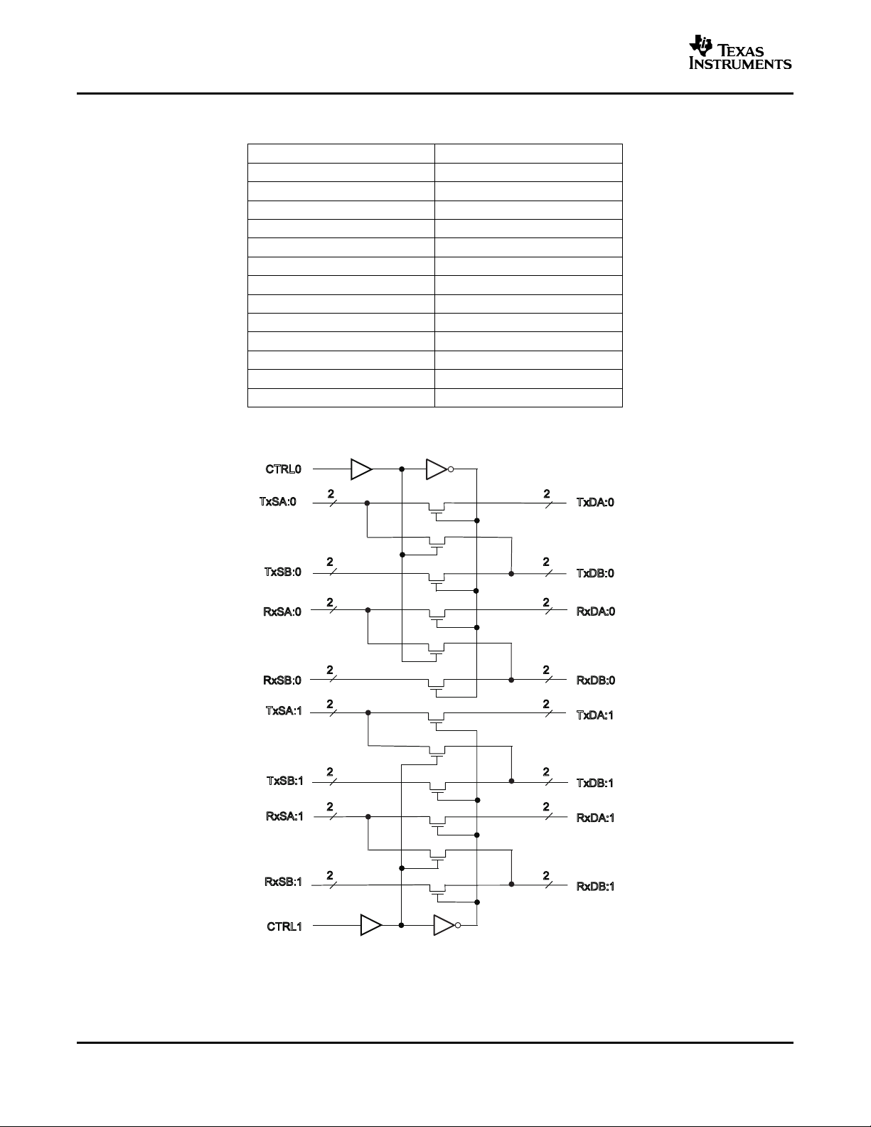
The TS2PCIE2212 can be used to muxltiplex/demultiplex two PCI Express™ lanes, each representing
differential pairs of receive (RX) and transmit (TX) signals. The switch operates at the PCI Express bandwidth
standard of 2.5-Gbps signal-processing speed. The device is composed of two banks, with each bank
accommodating two sources (source A and source B) and two destinations (destination A and destination B).
When a logic-level low is applied to the control (CTRL) pin, source A is connected to destination A and source B
is connected to destination B. When a logic-level high is applied to CTRL, source A is connected to destination
B, while source B and destination A are open.
• Minimal Propagation Delay
• ESD Performance Tested Per JESD 22
– 2000-V Human-Body Model
(A114-B, Class II)
– 1000-V Charged-Device Model (C101)
T
A
0 ° C to 85 ° C BGA – ZAH Tape and reel TS2PCIE2212ZAHR
1 2 3 4 5 6 7 8 9
A CTRL0 TxSB:0P TxSA:0P GND TxDA:0P TxDB:0P NC
B RxSA:0P GND TxSB:0N TxSA:0N VDD TxDA:0N TxDB:0N GND RxDA:0P
C RxSA:0N RxDA:0N
D RxSB:0P RxSB:0N RxDB:0N RxDB:0P
E GND VDD VDD GND
F TxSA:1P TxSA:1N TxDA:1N TxDA:1P
G TxSB:1N TxDB:1N
H TxSB:1P GND RxSA:1N RxSB:1N VDD RxDB:1N RxDA:1N GND TxDB:1P
J NC RxSA:1P RXSB:1P GND RXDB:1P RxDA:1P CTRL1
Please be aware that an important notice concerning availability, standard warranty, and use in critical applications of Texas
Instruments semiconductor products and disclaimers thereto appears at the end of this data sheet.
PCI Express is a trademark of PCI-SIG.
PRODUCTION DATA information is current as of publication date.
Products conform to specifications per the terms of the Texas
Instruments standard warranty. Production processing does not
necessarily include testing of all parameters.
ORDERING INFORMATION
PACKAGE ORDERABLE PART NUMBER TOP-SIDE MARKING
TERMINAL ASSIGNMENTS
Copyright © 2006, Texas Instruments Incorporated
Page 2
www.ti.com
TxDA:0
2
2
2
2
2
2
2
2
2
2
2
2
2
2
2
2
TxDB:0
RxDA:0
RxDB:0
TxDA:1
TxDB:1
RxDA:1
RxDB:1
TxSA:0
TxSB:0
RxSA:0
RxSB:0
TxSA:1
TxSB:1
RxSA:1
RxSB:1
CTRL1
CTRL0
TS2PCIE2212
PCI Express™ SIGNAL SWITCH
SCDS209 – JUNE 2006
PIN DESCRIPTION
NAME FUNCTION
TxSA:nP, TxSA:nN Source A transmit pair
RxSA:nP, RxSA:nN Source A receive pair
TxSB:nP, TxSB:nN Source B transmit pair
RxSB:nP, RxSB:nN Source B receive pair
TxDA:nP, TxDA:nN Destination A transmit pair
RxDA:nP, RxDA:nN Destination A receive pair
TxDB:nP, TxDB:nN Destination B transmit pair
RxDB:nP, RxDB:nN Destination B receive pair
CTRL0 Control signal for bank 0
CTRL1 Control signal for bank 1
V
DD
GND Ground (0 V)
NC No internal connection
Positive supply voltage
LOGIC DIAGRAM
2
Submit Documentation Feedback
Page 3
www.ti.com
FUNCTION TABLE
CTRLn FUNCTION
L SA:n = DA:n, SB:n = DB:n
H SA:n = DB:n, DA:n = open, SBin = open
TS2PCIE2212
PCI Express™ SIGNAL SWITCH
SCDS209 – JUNE 2006
Absolute Maximum Ratings
(1)
over operating free-air temperature range (unless otherwise noted)
MIN MAX UNIT
V
DD
V
IN
V
I/O
I
IK
I
I/OK
I
I/O
θ
JA
T
stg
Supply voltage range –0.5 2.5 V
Control input voltage range
Switch I/O voltage range
Control input clamp current VIN< 0 and V
I/O port clamp current VIN< 0 and V
ON-state switch current
Continuous current through V
Package thermal impedance
(2) (3)
(2) (3) (4)
< 0 50 mA
I/O
< 0 50 mA
(5)
or GND ± 100 mA
DD
(6)
I/O
–0.5 2.5 V
–0.5 2.5 V
± 100 mA
Storage temperature range –65 150 ° C
(1) Stresses beyond those listed under "absolute maximum ratings" may cause permanent damage to the device. These are stress ratings
only, and functional operation of the device at these or any other conditions beyond those indicated under "recommended operating
conditions" is not implied. Exposure to absolute-maximum-rated conditions for extended periods may affect device reliability.
(2) All voltages are with respect to ground, unless otherwise specified.
(3) The input and output voltage ratings may be exceeded if the input and output clamp-current ratings are observed.
(4) VIand VOare used to denote specific conditions for V
(5) IIand IOare used to denote specific conditions for I
(6) The package thermal impedance is calculated in accordance with JESD 51-7.
.
I/O
.
I/O
Recommended Operating Conditions
MIN TYP MAX UNIT
V
V
V
V
T
Supply voltage 1.7 1.8 1.9 V
DD
High-level control input voltage CTRL 0.65 V
IH
Low-level control input voltage CTRL 0.35 V
IL
Data input/output voltage 0 V
IO
Operating free-air temperature 0 85 ° C
A
DD
TBD ° C/W
V
V
DD
V
DD
Submit Documentation Feedback
3
Page 4
www.ti.com
TS2PCIE2212
PCI Express™ SIGNAL SWITCH
SCDS209 – JUNE 2006
Electrical Characteristics
over recommended operating free-air temperature range (unless otherwise noted)
PARAMETER TEST CONDITIONS UNIT
V
I
IN
I
OZ
I
CC
C
C
C
r
on
∆ r
IK
in
IO(OFF)
IO(ON)
on(flat)
Control inputs V
Control inputs V
Control inputs V
SB or DA port V
= 1.7 V, IIN= –18 mA –1.8 V
DD
= 1.9 V, VIN= V
DD
V
= 1.9 V, Switch OFF ± 5 µ A
DD
V
= 1.9 V,
DD
VIN= V
DD
I/O
V
I/O
V
DD
V
DD
V
DD
or GND,
DD
= 1.9 V, VIN= V
= 0 V, Switch OFF 1.4 1.5 pF
= 0 V, Switch ON 3.5 4 pF
= 1.7 V, VI= 0 V, IO= 10 mA 10 14
= 1.7 V, VI= 1.5 V, IO= –10 mA 12 17
= 1.7 V, IO= 10 mA, VI= 1.5 V ± 0.4 V 2.5 5 Ω
VO= 0 to 1.9 V,
VI= 0,
I
I/O
or GND ± 1 µ A
DD
= 0, Switch ON or OFF 160 300 µ A
or GND 0.5 1.0 pF
DD
Switching Characteristics
over recommended operating free-air temperature range (unless otherwise noted)
PARAMETER DESCRIPTION TEST CONDITIONS UNIT
DR Data rate per TX or RX pair 2.5 Gbps
t
pd
t
sk
ten(t
, t
PZL
PZH
t
(t
, t
dis
PLZ
PHZ
I
LOSS
R
LOSS
I
LOSS(CM)
O
IFF
X
TALK
Propagation delay, Sx to Dx See Figure 7 250 ps
Intra-pair skew f =1.25 GHz, See Figure 7 5 ps
) Switch turn-on delay, CTRL to DA See Figure 6 5 ns
) Switch turn-off delay, CTRL to DA See Figure 6 2.5 ns
Differential insertion loss –2.5 –3.2 dB
Differential return loss –7.2 –9.5 dB
Common-mode insertion loss –2 dB
Differential OFF isolation –33 –38 dB
Differential crosstalk –33 –39 dB
f =1.25 GHz, R
See Figure 1
f =1.25 GHz, R
See Figure 2
f =1.25 GHz, R
See Figure 3
f =1.25 GHz, R
See Figure 4
f =1.25 GHz, R
See Figure 5
= 50 Ω ,
LOAD
= 50 Ω ,
LOAD
= 50 Ω ,
LOAD
= 50 Ω ,
LOAD
= 50 Ω ,
LOAD
TA= 0 ° C to 85 ° C
MIN TYP MAX
TA= 0 ° C to 85 ° C
MIN TYP MAX
Ω
4
Submit Documentation Feedback
Page 5

www.ti.com
Frequency (GHz)
−6
−5
−4
−3
−2
−1
0
0.01 0.10 1.00 10.00
Decibel (dB)
Frequency (GHz)
−25
−20
−15
−10
−5
0
0.01 0.10 1.00 10.00
Decibel (dB)
Frequency (GHz)
−12
−10
−8
−6
−4
−2
0
0.01 0.10 1.00 10.00
Decibel (dB)
Frequency (GHz)
−80
−60
−40
−20
0
0.01 0.10 1.00 10.00
Decibel (dB)
Frequency (GHz)
−80
−60
−40
−20
0
0.01 0.10 1.00 10.00
Decibel (dB)
PCI Express™ SIGNAL SWITCH
OPERATING CHARACTERISTICS
Figure 1. Differential Insertion Loss vs Frequency Figure 2. Differential Return Loss vs Frequency
TS2PCIE2212
SCDS209 – JUNE 2006
Figure 3. Common-Mode Insertion Loss vs Frequency Figure 4. Differential OFF Isolation vs Frequency
Figure 5. Differential Crosstalk vs Frequency
Submit Documentation Feedback
5
Page 6

www.ti.com
C
L
(see Note A)
TEST CIRCUIT
S1
2 × V
DD
Open
GND
R
L
R
L
t
PZL
V
OH
− 0.3 V
VOLTAGE WAVEFORMS
ENABLE AND DISABLE TIMES
NOTES: A. CL includes probe and jig capacitance.
B. Waveform 1 is for an output with internal conditions such that the output is low, except when disabled by the output control.
Waveform 2 is for an output with internal conditions such that the output is high, except when disabled by the output control.
C. All input pulses are supplied by generators having the following characteristics: PRR ≤ 10 MHz, ZO = 50 Ω, tr ≤ 2.5 ns, tf ≤ 2.5 ns.
D. The outputs are measured one at a time, with one transition per measurement.
E. t
PLZ
and t
PHZ
are the same as t
dis
.
F. t
PZL
and t
PZH
are the same as ten.
50 Ω
V
G1
V
DD
DUT
50 Ω
V
IN
50 Ω
V
G2
V
I
TEST
R
L
S1 V
∆
C
L
V
CC
V
I
t
PLZ/tPZL
1.8 V ± 0.1 V 2 × V
DD
100 Ω GND No Load 0.3 V
Input Generator
Input Generator
VDD/2
VDD/2
V
O
t
PHZ/tPZH
1.8 V ± 0.1 V GND 100 Ω V
DD
No Load 0.3 V
Output Control
(VIN)
V
DD
V
OH
V
OL
+ 0.3 V
V
OH
V
OL
0 V
t
PZH
t
PLZ
t
PHZ
Output
Waveform 2
S1 at GND
(see Note B)
Output
Waveform 1
S1 at 2 y V
DD
(see Note B)
V
OL
SA
CTRL
VDD/2
VDD/2
TS2PCIE2212
PCI Express™ SIGNAL SWITCH
SCDS209 – JUNE 2006
PARAMETER MEASUREMENT INFORMATION
(Enable and Disable Times)
Figure 6. Test Circuit and Voltage Waveforms
6
Submit Documentation Feedback
Page 7

www.ti.com
PARAMETER MEASUREMENT INFORMATION
Sx:nP
TS2PCIE2212
Sx:nN
Dx:nP
Dx:nN
Input
Generator
V
I
V
O
V
COM
V
COM
+ 400 mV
Input
Waveform
Output
Waveform
t
PHL
t
PLH
V
COM
V
CRS
V
CRS
V
COM
− 400 mV
V
OH
V
OL
V
COM
= 1.5 V
tsk = |t
PLHn
– t
PHLn
|
V
CRS
is the cross point of the differential signal.
CTRL0
A1 GND
SA:n = DB:n, DA:n = open
TEST PATH
GNDSA:n = DA:n, SB:n = DB:n
V
DD
T1
(1)
(1) T1 is an external terminal.
V
DD
T1
(1)
V
DD
100 Ω
TS2PCIE2212
PCI Express™ SIGNAL SWITCH
SCDS209 – JUNE 2006
Figure 7. Test Circuit for Propagation Delay and Intra-Pair Skew
Submit Documentation Feedback
7
Page 8

www.ti.com
SA:nP
SA:nN
SB:nP
SB:nN
DA:nP
DA:nN
DB:nP
DB:nN
50 Ω
TS2PCIE2212
CTRL0
A1 GND
TEST
VNA
MEASUREMENT
Differential insertion loss
S
21
Differential return loss
S
11
Common-mode insertion loss
S
21
Network
Analyzer
50 Ω
V
DD
V
DD
50 Ω
50 Ω
TS2PCIE2212
PCI Express™ SIGNAL SWITCH
SCDS209 – JUNE 2006
PARAMETER MEASUREMENT INFORMATION (continued)
Figure 8. Differential Insertion Loss, Differential Return Loss,
and Common-Mode Insertion Loss Test Circuit
8
Submit Documentation Feedback
Page 9

www.ti.com
50 Ω
TxSA:0P
TxSA:0N
TxSB:0P
TxSB:0N
TxDA:0P
TxDA:0N
TxDB:0P
TxDB:0N
A4
B4
A2
B3
A6
B6
A8
B7
50 Ω
50 Ω
TS2PCIE2212
CTRL0
A1 GND
TEST
Differential crosstalk GND
Differential OFF isolation
V
DD
Network
Analyzer
V
DD
V
DD
50 Ω
T1
(1)
T1
(1)
(1) T1 is an external terminal.
PARAMETER MEASUREMENT INFORMATION (continued)
TS2PCIE2212
PCI Express™ SIGNAL SWITCH
SCDS209 – JUNE 2006
Figure 9. Differential Crosstalk and OFF Isolation Test Circuit
Submit Documentation Feedback
9
Page 10

PACKAGE OPTION ADDENDUM
www.ti.com
13-Mar-2008
PACKAGING INFORMATION
Orderable Device Status
(1)
Package
Type
Package
Drawing
Pins Package
Qty
Eco Plan
TS2PCIE2212ZAHR ACTIVE NFBGA ZAH 48 3000 Pb-Free
(1)
The marketing status values are defined as follows:
ACTIVE: Product device recommended for new designs.
LIFEBUY: TI has announced that the device will be discontinued, and a lifetime-buy period is in effect.
NRND: Not recommended for new designs. Device is in production to support existing customers, but TI does not recommend using this part in
a new design.
PREVIEW: Device has been announced but is not in production. Samples may or may not be available.
OBSOLETE: TI has discontinued the production of the device.
(2)
Eco Plan - The planned eco-friendly classification: Pb-Free (RoHS), Pb-Free (RoHS Exempt), or Green (RoHS & no Sb/Br) - please check
http://www.ti.com/productcontent for the latest availability information and additional product content details.
TBD: The Pb-Free/Green conversion plan has not been defined.
Pb-Free (RoHS): TI's terms "Lead-Free" or "Pb-Free" mean semiconductor products that are compatible with the current RoHS requirements
for all 6 substances, including the requirement that lead not exceed 0.1% by weight in homogeneous materials. Where designed to be soldered
at high temperatures, TI Pb-Free products are suitable for use in specified lead-free processes.
Pb-Free (RoHS Exempt): This component has a RoHS exemption for either 1) lead-based flip-chip solder bumps used between the die and
package, or 2) lead-based die adhesive used between the die and leadframe. The component is otherwise considered Pb-Free (RoHS
compatible) as defined above.
Green (RoHS & no Sb/Br): TI defines "Green" to mean Pb-Free (RoHS compatible), and free of Bromine (Br) and Antimony (Sb) based flame
retardants (Br or Sb do not exceed 0.1% by weight in homogeneous material)
(RoHS)
(2)
Lead/Ball Finish MSL Peak Temp
SNAGCU Level-3-260C-168 HR
(3)
(3)
MSL, Peak Temp. -- The Moisture Sensitivity Level rating according to the JEDEC industry standard classifications, and peak solder
temperature.
Important Information and Disclaimer:The information provided on this page represents TI's knowledge and belief as of the date that it is
provided. TI bases its knowledge and belief on information provided by third parties, and makes no representation or warranty as to the
accuracy of such information. Efforts are underway to better integrate information from third parties. TI has taken and continues to take
reasonable steps to provide representative and accurate information but may not have conducted destructive testing or chemical analysis on
incoming materials and chemicals. TI and TI suppliers consider certain information to be proprietary, and thus CAS numbers and other limited
information may not be available for release.
In no event shall TI's liability arising out of such information exceed the total purchase price of the TI part(s) at issue in this document sold by TI
to Customer on an annual basis.
Addendum-Page 1
Page 11
Page 12

IMPORTANT NOTICE
Texas Instruments Incorporated and its subsidiaries (TI) reserve the right to make corrections, modifications, enhancements, improvements,
and other changes to its products and services at any time and to discontinue any product or service without notice. Customers should
obtain the latest relevant information before placing orders and should verify that such information is current and complete. All products are
sold subject to TI’s terms and conditions of sale supplied at the time of order acknowledgment.
TI warrants performance of its hardware products to the specifications applicable at the time of sale in accordance with TI’s standard
warranty. Testing and other quality control techniques are used to the extent TI deems necessary to support this warranty. Except where
mandated by government requirements, testing of all parameters of each product is not necessarily performed.
TI assumes no liability for applications assistance or customer product design. Customers are responsible for their products and
applications using TI components. To minimize the risks associated with customer products and applications, customers should provide
adequate design and operating safeguards.
TI does not warrant or represent that any license, either express or implied, is granted under any TI patent right, copyright, mask work right,
or other TI intellectual property right relating to any combination, machine, or process in which TI products or services are used. Information
published by TI regarding third-party products or services does not constitute a license from TI to use such products or services or a
warranty or endorsement thereof. Use of such information may require a license from a third party under the patents or other intellectual
property of the third party, or a license from TI under the patents or other intellectual property of TI.
Reproduction of TI information in TI data books or data sheets is permissible only if reproduction is without alteration and is accompanied
by all associated warranties, conditions, limitations, and notices. Reproduction of this information with alteration is an unfair and deceptive
business practice. TI is not responsible or liable for such altered documentation. Information of third parties may be subject to additional
restrictions.
Resale of TI products or services with statements different from or beyond the parameters stated by TI for that product or service voids all
express and any implied warranties for the associated TI product or service and is an unfair and deceptive business practice. TI is not
responsible or liable for any such statements.
TI products are not authorized for use in safety-critical applications (such as life support) where a failure of the TI product would reasonably
be expected to cause severe personal injury or death, unless officers of the parties have executed an agreement specifically governing
such use. Buyers represent that they have all necessary expertise in the safety and regulatory ramifications of their applications, and
acknowledge and agree that they are solely responsible for all legal, regulatory and safety-related requirements concerning their products
and any use of TI products in such safety-critical applications, notwithstanding any applications-related information or support that may be
provided by TI. Further, Buyers must fully indemnify TI and its representatives against any damages arising out of the use of TI products in
such safety-critical applications.
TI products are neither designed nor intended for use in military/aerospace applications or environments unless the TI products are
specifically designated by TI as military-grade or "enhanced plastic." Only products designated by TI as military-grade meet military
specifications. Buyers acknowledge and agree that any such use of TI products which TI has not designated as military-grade is solely at
the Buyer's risk, and that they are solely responsible for compliance with all legal and regulatory requirements in connection with such use.
TI products are neither designed nor intended for use in automotive applications or environments unless the specific TI products are
designated by TI as compliant with ISO/TS 16949 requirements. Buyers acknowledge and agree that, if they use any non-designated
products in automotive applications, TI will not be responsible for any failure to meet such requirements.
Following are URLs where you can obtain information on other Texas Instruments products and application solutions:
Products Applications
Amplifiers amplifier.ti.com Audio www.ti.com/audio
Data Converters dataconverter.ti.com Automotive www.ti.com/automotive
DSP dsp.ti.com Broadband www.ti.com/broadband
Clocks and Timers www.ti.com/clocks Digital Control www.ti.com/digitalcontrol
Interface interface.ti.com Medical www.ti.com/medical
Logic logic.ti.com Military www.ti.com/military
Power Mgmt power.ti.com Optical Networking www.ti.com/opticalnetwork
Microcontrollers microcontroller.ti.com Security www.ti.com/security
RFID www.ti-rfid.com Telephony www.ti.com/telephony
RF/IF and ZigBee® Solutions www.ti.com/lprf Video & Imaging www.ti.com/video
Mailing Address: Texas Instruments, Post Office Box 655303, Dallas, Texas 75265
Copyright © 2008, Texas Instruments Incorporated
Wireless www.ti.com/wireless
 Loading...