

www.ti.com
3
2
4
5
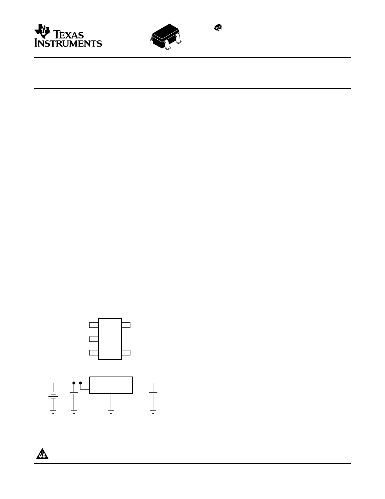
DBV PACKAGE
(TOP VIEW)
1
IN
GND
EN
OUT
NC/FB
TPS72115
0.1 µF 0.1 µF
1.8 V 1.5 V
GND
OUTIN
EN
LOW INPUT VOLTAGE, CAP FREE 150-mA
LOW-DROPOUT LINEAR REGULATORS
FEATURES DESCRIPTION
• 150-mA LDO
• Available in 1.5-V, 1.6-V, 1.8-V Fixed-Output
and Adjustable (1.2-V to 2.5-V) Versions
• Low Input Voltage Requirement (Down to
1.8 V)
• Small Output Capacitor, 0.1-µF
• Dropout Voltage Typically 200 mV at 150 mA
• Less Than 1 µA Quiescent Current in
Shutdown Mode
• Thermal Protection
• Over Current Limitation
• 5-Pin SOT-23 (DBV) Package
APPLICATIONS
• Portable Communication Devices
• Battery Powered Equipment
• PCMCIA Cards
• Personal Digital Assistants
• Modems
• Bar Code Scanners
• Backup Power Supplies
• SMPS Post Regulation
• Internet Audio
TPS72101 , , TPS72115
TPS72116 , TPS72118
SLVS352C – DECEMBER 2001 – REVISED MARCH 2006
The TPS721xx family of LDO regulators is available
in fixed voltage options that are commonly used to
power the latest DSPs and microcontrollers with an
adjustable option ranging from 1.22 V to 2.5 V. These
regulators can be used in a wide variety of
applications ranging from portable, battery-powered
equipment to PC peripherals. The family features
operation over a wide range of input voltages (1.8 V
to 5.5 V) and low dropout voltage (150 mV at full
load). Therefore, compared to many other regulators
that require 2.5-V or higher input voltages for
operation, these regulators can be operated directly
from two AAA batteries. Also, the typical quiescent
current (ground pin current) is low, starting at 85 µA
during normal operation and 1 µA in shutdown mode.
These regulators can be operated very efficiently and,
in a battery-powered application, help extend the
longevity of the device.
Similar LDO regulators require 1-µF or larger output
capacitors for stability. However, this regulator uses
an internal compensation scheme that stabilizes the
feedback loop over the full range of input voltages
and load currents with output capacitances as low as
0.1-µF. Ceramic capacitors of this size are relatively
inexpensive and available in small footprints.
This family of regulators is particularly suited as a
portable power supply solution due to its minimal
board space requirement and 1.8-V minimum input
voltage. Being able to use two off-the-shelf AAA
batteries makes system design easier and also
reduces component cost. Moreover, the solution will
be more efficient than if a regulator with a higher
input voltage is used.
Please be aware that an important notice concerning availability, standard warranty, and use in critical applications of Texas
Instruments semiconductor products and disclaimers thereto appears at the end of this data sheet.
PRODUCTION DATA information is current as of publication date.
Products conform to specifications per the terms of the Texas
Instruments standard warranty. Production processing does not
necessarily include testing of all parameters.
Copyright © 2001–2006, Texas Instruments Incorporated
www.ti.com
TPS72101 , , TPS72115
TPS72116 , TPS72118
SLVS352C – DECEMBER 2001 – REVISED MARCH 2006
These devices have limited built-in ESD protection. The leads should be shorted together or the device placed in conductive foam
during storage or handling to prevent electrostatic damage to the MOS gates.
ORDERING INFORMATION
T
J
-40°C to 125°C
(1) The DBVT indicates tape and reel of 250 parts.
(2) The DBVR indicates tape and reel of 3000 parts.
ABSOLUTE MAXIMUM RATINGS
over operating free-air temperature range unless otherwise noted
Voltage range at IN -0.3 V to 7 V
Voltage range at EN -0.3 V to 7 V
Voltage on OUT, FB, NC -0.3 V to VI+ 0.3 V
Peak output current Internally limited
ESD rating, HBM 3 kV
Continuous total power dissipation See Dissipation Rating Table
Operating junction temperature range, T
Storage temperature range, T
(1) Stresses beyond those listed under absolute maximum ratings may cause permanent damage to the device. These are stress ratings
only, and functional operation of the device at these or any other conditions beyond those indicated under recommended operating
conditions is not implied. Exposure to absolute-maximum-rated conditions for extended periods may affect device reliability.All voltage
values are with respect to network ground terminal.
(2) All voltage values are with respect to network ground terminal.
VOLTAGE PACKAGE PART NUMBER SYMBOL
Adjustable TPS72101DBVT
1.5 V TPS72115DBVT
1.6 V TPS72116DBVT
1.8 V TPS72118DBVT
J
stg
SOT-23
(DBV)
(1) (2)
(1)
(1)
(1)
(1)
TPS72101DBVR
TPS72115DBVR
TPS72116DBVR
TPS72118DBVR
(2)
(2)
(2)
(2)
TPS72101, TPS72115,
TPS72116, TPS72118
-40°C to 150°C
-65°C to 150°C
PEKI
PEII
PHFI
PEJI
PACKAGE DISSIPATION RATING
BOARD PACKAGE R
(1)
Low-K
(2)
High-K
DBV 65.8 °C/W 259 °C/W 3.9 mW/°C 386 mW 212 mW 154 mW
DBV 65.8 °C/W 180 °C/W 5.6 mW/°C 555 mW 305 mW 222 mW
Θ JC
R
Θ JA
(1) The JEDEC Low-K (1s) board design used to derive this data was a 3 inch x 3 inch, two-layer board with 2 ounce copper traces on top
of the board.
(2) The JEDEC High-K (2s2p) board design used to derive this data was a 3 inch x 3 inch, multilayer board with 1 ounce internal power and
ground planes and 2 ounce copper traces on top and bottom of the board.
2
DERATING FACTOR TA≤ 25°C TA= 70°C TA= 85°C
ABOVE TA= 25°C POWER RATING POWER RATING POWER RATING
Submit Documentation Feedback
www.ti.com
ELECTRICAL CHARACTERISTICS
over recommended operating junction temperature range V
otherwise noted)
PARAMETER TEST CONDITIONS MIN TYP MAX UNIT
V
V
I
T
V
I
Input voltage
IN
Output voltage range TPS72101 1.225 2.5 V
OUT
Continuous output current 0 150 mA
OUT
Operating junction temperature -40 125 °C
J
Output voltage TJ= 25°C 1.6 V
OUT
Quiescent current (GND current) µA
(Q)
Standby current µA
V
V
PSRR
Output noise voltage TPS72115 Co= 1 µF 90 µV
n
Reference voltage TJ= 25°C 1.225 V
ref
Ripple rejection TJ= 25°C; See
Current limit See
Output voltage line regulation
( ∆ V
OUT
Output voltage load
regulation
V
V
I
V
I
EN high level input 1.4
IH
EN low level input -0.2 0.4
IL
EN input current µA
I
Dropout voltage
DO
Feedback input current TPS72101 1 µA
n
Thermal shutdown temperature 170 °C
Thermal shutdown hysteresis 20 °C
(1)
TPS72101 0 µA < I
TPS72115
TPS72116
TPS72118
TJ= 25°C 1.5
0 µA < I
0 µA < I
TJ= 25°C 1.8
0 µA < I
< 150 mA
OUT
< 150 mA 2.5 V ≤ VIN≤ 5.5 V 1.455 1.545
OUT
< 150 mA 2.6 V ≤ VIN≤ 5.5 V 1.552 1.648
OUT
< 150 mA 2.8 V ≤ VIN≤ 5.5 V 1.746 1.854
OUT
TJ= 25°C 85
I
= 150 mA TJ= 25°C 570
OUT
I
= 150 mA 850
OUT
EN < 0.5 V TJ= 25°C 0.01
EN < 0.5 V 1
BW = 200 Hz to 100 kHz, T
= 25°C
f = 100 Hz, Co= 10 µF, I
= 150 mA
(2)
(1)
/V
)
OUT
TPS72118 0 < I
VO+ 1 V < VIN≤ 2.5 V %/V
< 150 mA TJ= 25°C 0.5 mV
OUT
EN = 0 V -0.01
EN = IN -0.01
(3)
TPS72118 I
TPS72101 I
= 150 mA TJ= 25°C 150
OUT
= 150 mA 1.2 V ≤ VO≤ 5.2 V 240
OUT
TPS72101 , , TPS72115
TPS72116 , TPS72118
SLVS352C – DECEMBER 2001 – REVISED MARCH 2006
= V
IN
OUT(Nom)
(1)
OUT
+ 1 V, I
= 1 mA, EN = VIN, C
OUT
1.8 5.5 V
1.8 V ≤ V
J
≤ 2.5 V 0.97 V
OUT
(1)
O
175 525 mA
TJ= 25°C 0.03 0.09
= 1 µF (unless
OUT
1.03 V
O
120
48 dB
0.1
V
mV
(1) Minimum IN operating voltage is 1.8 V or V
(2) Test condition includes output voltage VO= 1 V and pulse duration = 10 mS.
+ VDO, whichever is greater.
OUT
(3) Dropout voltage is defined as the differential voltage between VOand VIwhen VOdrops 100 mV below the value measured with VIN=
V
+ VDO.
OUT
Submit Documentation Feedback
3
www.ti.com
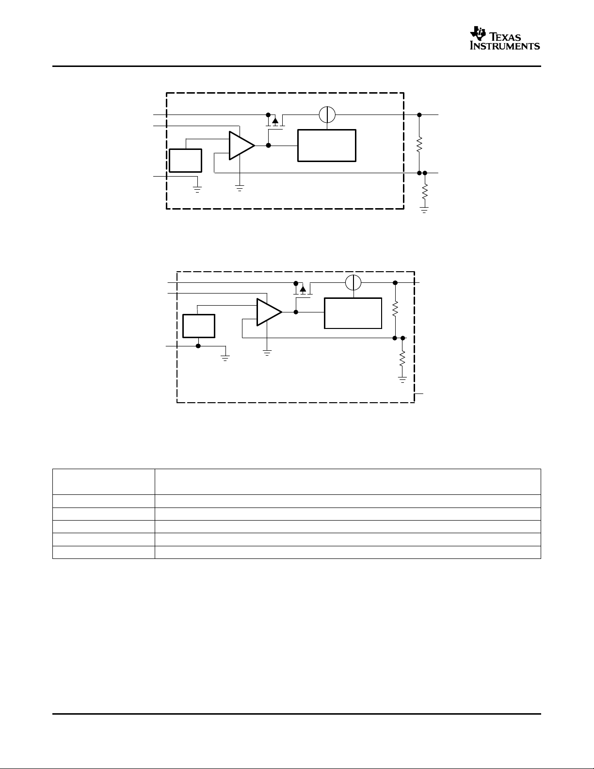
TPS72101
OUT
IN
FB
GND
EN
Current Limit /
Thermal
Protection
V
REF
1.225V
TPS72115/16/18
OUT
IN
GND
EN
Current Limit /
Thermal
Protection
NC
(A)
V
REF
1.225V
TPS72101 , , TPS72115
TPS72116 , TPS72118
SLVS352C – DECEMBER 2001 – REVISED MARCH 2006
Figure 1. FUNCTIONAL BLOCK DIAGRAM—ADJUSTABLE VERSION
A. This pin must be left floating and not connected to GND.
Figure 2. FUNCTIONAL BLOCK DIAGRAM—FIXED VERSION
Terminal Functions
TERMINAL
NAME NO.
GND 2 Ground
EN 3 Enable input
IN 1 Input supply voltage
NC/FB 4 NC = Not connected (see
OUT 5 Regulated output voltage
4
(A)
); FB = Feedback (adjustable option TPS72101)
Submit Documentation Feedback
DESCRIPTION
www.ti.com
1.7995
1.7996
1.7997
1.7998
1.7999
1.8000
1.8001
1.8002
0 30 60 90 120 150
I
O
− Output Current − mA
− Output Voltage − V
V
O
VI = 2.8 V
Co = 1 µF
TJ = 25° C
TJ − Junction Temperature − °C
− Output Voltage − V
V
O
IO = 150 mA
IO = 1 mA
VI = 2.8 V
Co = 1 µF
1.7900
1.7920
1.7940
1.7960
1.7980
1.8000
1.8020
1.8040
−40−25−10 5 20 35 50 65 80 95 110 125
0
100
200
300
400
500
600
700
−40−25−10 5 20 35 50 65 80 95 110 125
T
J
− Junction Temperature − °C
Ground Current −
IO = 150 mA
VI = 2.8 V
Co = 1 µF
IO = 1 mA
Aµ
f − Frequency − Hz
IO = 1 mA
VI = 2.8 V
Co = 1 µF
IO = 150 mA
Output Impedance − Ω
1
0.1
0.01
1 10 100 1 k 10 k10100 k 1 M 10 M
0.001
100
1 k
0
100
300
400
500
600
700
I
O
− Output Current − mA
Ground Current − Aµ
TJ = 25° C
TJ = 125° C
0 60 90 120 150
TJ = −40° C
VI = 2.8 V
Co = 1 µF
30
200
0
0.5
1
1.5
2
2.5
100 1 k 10 k 100 k
f − Frequency − Hz
IO = 1 mA
VI = 2.8 V
Co = 1 µF
IO = 150 mA
V/ HzOutput Spectral Noise Density −
µ
SLVS352C – DECEMBER 2001 – REVISED MARCH 2006
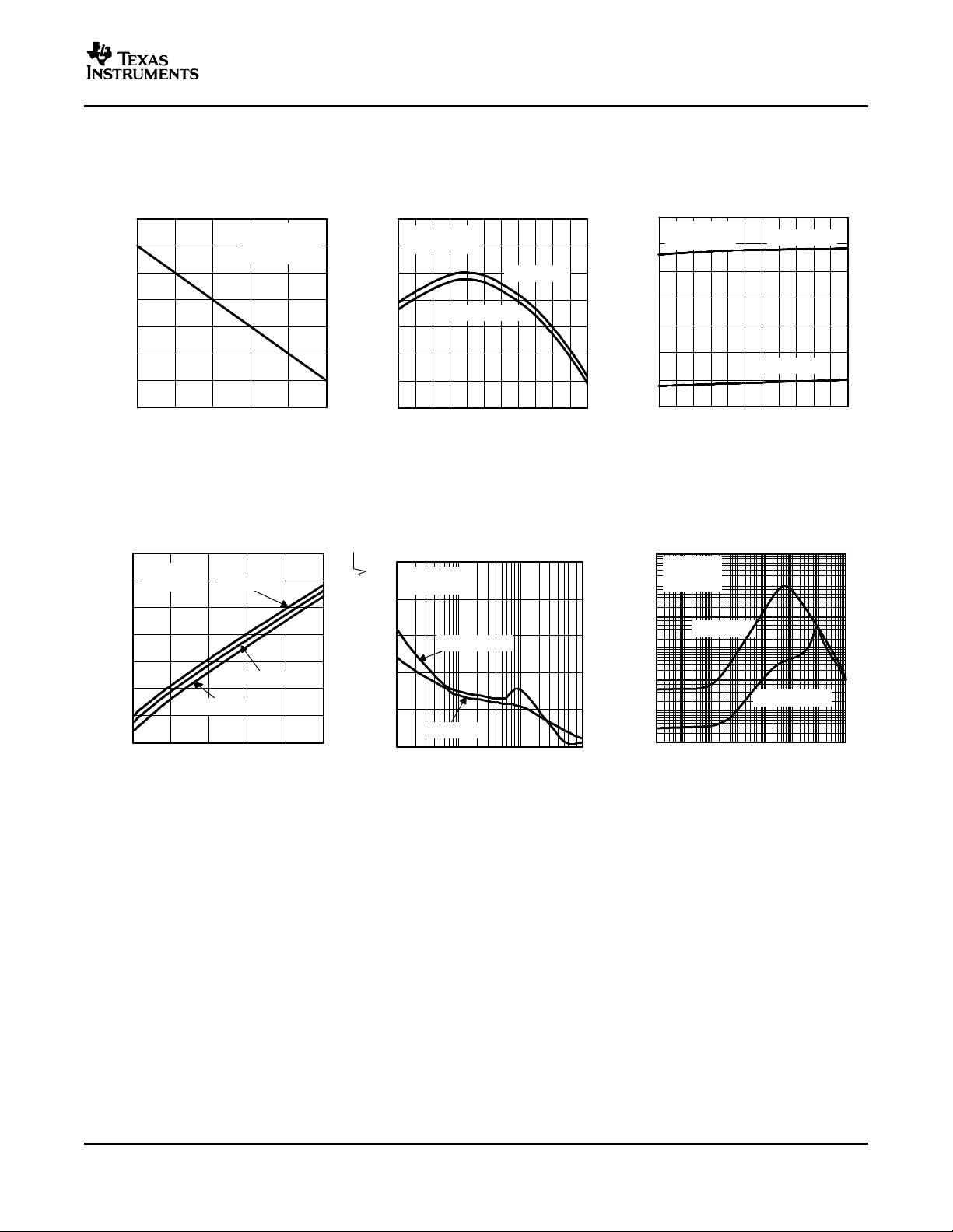
TYPICAL CHARACTERISTICS
TPS72118 TPS72118 TPS72118
OUTPUT VOLTAGE OUTPUT VOLTAGE GROUND CURRENT
vs vs vs
OUTPUT CURRENT JUNCTION TEMPERATURE JUNCTION TEMPERATURE
Figure 3. Figure 4. Figure 5.
TPS72101 , , TPS72115
TPS72116 , TPS72118
TPS72118 TPS72118 TPS72118
GROUND CURRENT OUTPUT SPECTRAL NOISE OUTPUT IMPEDANCE
vs DENSITY vs
OUTPUT CURRENT vs FREQUENCY
FREQUENCY
Figure 6. Figure 7. Figure 8.
Submit Documentation Feedback
5

www.ti.com
IO = 150 mA
IO = 10 mA
VI = 2.8 V
Co = 1 µF
T
J
− Junction Temperature − °C
− Dropout Voltage − mV
V
DO
0
50
100
150
200
250
−40−25−10 5 20 35 50 65 80 95 110 125
V
O
t − Time − µs
0 15010050 200 200 350300 400 450 500
− Output Voltage − V
VI = 2.8 V
VO = 1.8 V
IO = 150 mA
Co = 1 µF
Enable Voltage − V
1
2
1
0
2
3
V
EN
V
O
0
0
10
20
30
40
50
60
70
1 10 100 1 k 10 k 100 k 1 M
Power Supply Ripple Rejection − dB
f − Frequency − Hz
VI = 2.8 V
Co = 1 µF
IO = 150 mA
Power Up / Power Down − V
V
I
V
O
Co = 1 µF
Ci = 1 µF
RL = 12 Ω
0
1
2
3
4
5
6
t − Time − ms
0 302010 40 50 7060 80 90 100
V
I
t − Time − ms
0 0.30.20.1 0.4 0.5 0.70.6 0.8 0.9 1
− Input Voltage − VV
O
− Output Voltage −V
0
-1
2.8
1
3.8
IO = 150 mA
Co = 1 µF
dV
I
dt
0.4 V
µs
V
I
V
O
0.2
t − Time − ms
0
0 0.30.1 0.4 0.5 0.70.6 0.8 0.9
100
0
−100
V
O
Output Voltage − mV
∆
− Change In
50
1
− Output Current − mA
I
O
VI = 2.8 V
Co = 1 µF
100
150
dI
O
dt
0.1A
µs
0
50
100
150
200
250
1.8 2.5 3.3 4 4.8 5.5
V
I
− Input Voltage − V
− Dropout Voltage − mV
V
DO
TJ = 25°C
TJ = −40°C
TJ = 125°C
IO = 150 mA
DC Dropout Voltage − mV
IO − Output Current − mA
TJ = 125°C
TJ = 25°C
TJ = −40°C
0
50
100
150
200
250
0
15 30 45 60 75 90 105 120 135 150
1
1.5
2
2.5
3
3.5
4
4.5
5
5.5
1 1.5 2 2.5 3 3.5 4 4.5 5 5.5
TJ = 25°C
IO = 150 mA
− Minimum Required Input Voltage − V
VO − Output Voltage − V
V
I
TJ = 125°C
TJ = −40°C
TPS72101 , , TPS72115
TPS72116 , TPS72118
SLVS352C – DECEMBER 2001 – REVISED MARCH 2006
TPS72118 TPS72118 TPS72118
DROPOUT VOLTAGE POWER SUPPLY RIPPLE OUTPUT VOLTAGE, ENABLE
vs REJECTION VOLTAGE
JUNCTION TEMPERATURE vs vs
Figure 9. Figure 10. Figure 11.
TYPICAL CHARACTERISTICS (continued)
FREQUENCY TIME (START-UP)
LINE TRANSIENT RESPONSE LOAD TRANSIENT RESPONSE
TPS72118 TPS72118 POWER UP / POWER DOWN
Figure 12. Figure 13. Figure 14.
DC DROPOUT VOLTAGE TPS72101 MINIMUM REQUIRED INPUT
vs DROPOUT VOLTAGE VOLTAGE
OUTPUT CURRENT vs vs
INPUT VOLTAGE OUTPUT VOLTAGE
6
Figure 15. Figure 16. Figure 17.
Submit Documentation Feedback

www.ti.com
NC
OUT
1
3
IN
EN
GND
2
4
5
V
I
V
O
0.1 µF
TPS721xx
0.1 µF
TPS72101 , , TPS72115
TPS72116 , TPS72118
SLVS352C – DECEMBER 2001 – REVISED MARCH 2006
APPLICATION INFORMATION
The TPS721xx family of low-dropout (LDO) regulators functions with a very low input voltage (>1.8 V). The
dropout voltage is typically 150 mV at full load. Typical quiescent current (ground pin current) is only 85 µA and
drops to 1 µA in the shutdown mode.
DEVICE OPERATION
The TPS721xx family can be operated at low input voltages due to low voltage circuit design techniques and a
PMOS pass element that exhibits low dropout.
A logic low on the enable input, EN, shuts off the output and reduces the supply current to less than 1 µA. EN
may be tied to V
Current limiting and thermal protection prevent damage by excessive output current and/or power dissipation.
The device switches into a constant-current mode at approximately 350 mA; further load reduces the output
voltage instead of increasing the output current. The thermal protection shuts the regulator off if the junction
temperature rises above 170°C. Recovery is automatic when the junction temperature drops approximately 20°C
below the high temperature trip point. The PMOS pass element includes a back diode that safely conducts
reverse current when the input voltage level drops below the output voltage level.
A typical application circuit is shown in Figure 18 .
in applications where the shutdown feature is not used.
IN
Figure 18. Typical Application Circuit
DUAL SUPPLY APPLICATION
In portable, battery-powered electronics, separate power rails for the DSP or microcontroller core voltage,
V
for providing V
voltage to a boost converter and the TPS72115 LDO linear regulator. The batteries combine input voltage ranges
from 3.0 V down to 1.8 V near the end of their useful lives. Therefore, a boost converter is necessary to provide
the typical 3.3 V needed for V
in this example is 1.5 V. Although there is no explicit circuitry to perform power-up sequencing of first V
then V
any switching type boost converter due to the inherent slow start up of those types of converters. Assuming a
boost converter with minimum VIof 1.8 V is appropriately chosen, this power supply solution can be used over
the entire life of the two off-the-shelf AAA batteries. Thus, this solution is very efficient and the design time and
overall cost of the solution is minimized.
, and I/O peripherals (V
(CORE)
, the output of the linear regulator reaches its regulated voltage much faster (< 400 µs) than the output of
IO
for the DSP or microcontroller. As shown in Figure 19 , two AAA batteries provide an input
(CORE)
) are usually necessary. The TPS721xx family of LDO linear regulators is ideal
IO
, and the TPS72115 linear regulator provides a regulated V
IO
Submit Documentation Feedback
(CORE)
voltage, which
(CORE)
7

www.ti.com
TPS72115
1.8 V 1.5 V
Boost Converter
3.3 V
1.8 V – 3 V
V
IO
V
CORE
DSP or
Controller
Two AAA
Batteries
P
D(max)
TJmax T
A
R
JA
P
D
VI V
O
I
O
VO V
ref
1
R1
R2
TPS72101 , , TPS72115
TPS72116 , TPS72118
SLVS352C – DECEMBER 2001 – REVISED MARCH 2006
APPLICATION INFORMATION (continued)
Figure 19. Dual Supply Application Circuit
EXTERNAL CAPACITOR REQUIREMENTS
A 0.1-µF ceramic bypass capacitor is required on both the input and output for stability. Larger capacitors
improve transient response, noise rejection, and ripple rejection. A higher value electrolytic input capacitor may
be necessary if large, fast rise time load transient are anticipated, and/or there is significant input resistance from
the device to the input power supply.
POWER DISSIPATION AND JUNCTION TEMPERATURE
Specified regulator operation is assured to a junction temperature of 125°C; the maximum junction temperature
allowable without damaging the device is 150°C. This restriction limits the power dissipation the regulator can
handle in any given application. To ensure the junction temperature is within acceptable limits, calculate the
maximum allowable dissipation, P
P
.
D(max)
, and the actual dissipation, PD, which must be less than or equal to
D(max)
The maximum-power-dissipation limit is determined using Equation 1 :
Where:
• TJmax is the maximum allowable junction temperature.
• R
• TAis the ambient temperature.
is the thermal resistance junction-to-ambient for the package; see the package dissipation rating table.
θ JA
The regulator dissipation is calculated using Equation 2 :
Power dissipation resulting from quiescent current is negligible.
PROGRAMMING THE TPS72101 ADJUSTABLE LDO REGULATOR
The output voltage of the TPS72101 adjustable regulator is programmed using an external resistor divider as
shown in Figure 20 . The output voltage is calculated using Equation 3 :
(1)
(2)
Where:
• V
8
= 1.225 V typ (the internal reference voltage)
ref
Submit Documentation Feedback
(3)

www.ti.com
R1
V
O
V
ref
1 R2
V
O
V
I
OUT
FB
R2
GND
EN
IN
≤0.9 V
≥1.7 V
TPS72101
OUTPUT
VOLTAGE
(V)
R1 R2
2.5 127 121
OUTPUT VOLTAGE
PROGRAMMING GUIDE
DIVIDER RESISTANCE
(kΩ)
1
Note (1): 1% values shown.
3
1
4
2
R1
5
0.1 µF
0.1 µF
TPS72101 , , TPS72115
TPS72116 , TPS72118
SLVS352C – DECEMBER 2001 – REVISED MARCH 2006
APPLICATION INFORMATION (continued)
Resistors R1 and R2 should be chosen for approximately 10-µA divider current. Lower value resistors can be
used but offer no inherent advantage and waste more power. Higher values should be avoided, as leakage
currents at FB increase the output voltage error. The recommended design procedure is to choose R2 = 30.1 k Ω
to set the divider current at 10 µA and then calculate R1 using Equation 4 :
Where:
• V
ref
= 1.225 V.
(4)
REGULATOR PROTECTION
The TPS721xx pass element has a built-in back diode that safely conducts reverse current when the input
voltage drops below the output voltage (for example, during power down). Current is conducted from the output
to the input and is not internally limited. If extended reverse voltage is anticipated, external limiting might be
appropriate.
The TPS721xx also features internal current limiting and thermal protection. During normal operation, the
TPS721xx limits output current to approximately 350 mA. When current limiting engages, the output voltage
scales back linearly until the overcurrent condition ends. While current limiting is designed to prevent gross
device failure, care should be taken not to exceed the power dissipation ratings of the package. If the
temperature of the device exceeds 170°C, thermal-protection circuitry shuts it down. Once the device has cooled
down to below 150°C, regulator operation resumes.
Figure 20. TPS72101 Adjustable LDO Regulator Programming
Submit Documentation Feedback
9

PACKAGE OPTION ADDENDUM
www.ti.com
5-Feb-2007
PACKAGING INFORMATION
Orderable Device Status
(1)
Package
Type
Package
Drawing
Pins Package
Qty
Eco Plan
TPS72101DBVR ACTIVE SOT-23 DBV 5 3000 Green (RoHS &
no Sb/Br)
TPS72101DBVRG4 ACTIVE SOT-23 DBV 5 3000 Green (RoHS &
no Sb/Br)
TPS72101DBVT ACTIVE SOT-23 DBV 5 250 Green (RoHS &
no Sb/Br)
TPS72101DBVTG4 ACTIVE SOT-23 DBV 5 250 Green (RoHS &
no Sb/Br)
TPS72115DBVR ACTIVE SOT-23 DBV 5 3000 Green (RoHS &
no Sb/Br)
TPS72115DBVRG4 ACTIVE SOT-23 DBV 5 3000 Green (RoHS &
no Sb/Br)
TPS72115DBVT ACTIVE SOT-23 DBV 5 250 Green (RoHS &
no Sb/Br)
TPS72115DBVTG4 ACTIVE SOT-23 DBV 5 250 Green (RoHS &
no Sb/Br)
TPS72116DBVR ACTIVE SOT-23 DBV 5 3000 Green (RoHS &
no Sb/Br)
TPS72116DBVRG4 ACTIVE SOT-23 DBV 5 3000 Green (RoHS &
no Sb/Br)
TPS72116DBVT ACTIVE SOT-23 DBV 5 250 Green (RoHS &
no Sb/Br)
TPS72116DBVTG4 ACTIVE SOT-23 DBV 5 250 Green (RoHS &
no Sb/Br)
TPS72118DBVR ACTIVE SOT-23 DBV 5 3000 Green (RoHS &
no Sb/Br)
TPS72118DBVRG4 ACTIVE SOT-23 DBV 5 3000 Green (RoHS &
no Sb/Br)
TPS72118DBVT ACTIVE SOT-23 DBV 5 250 Green (RoHS &
no Sb/Br)
TPS72118DBVTG4 ACTIVE SOT-23 DBV 5 250 Green (RoHS &
no Sb/Br)
(1)
The marketing status values are defined as follows:
ACTIVE: Product device recommended for new designs.
LIFEBUY: TI has announced that the device will be discontinued, and a lifetime-buy period is in effect.
NRND: Not recommended for new designs. Device is in production to support existing customers, but TI does not recommend using this part in
a new design.
PREVIEW: Device has been announced but is not in production. Samples may or may not be available.
OBSOLETE: TI has discontinued the production of the device.
(2)
Lead/Ball Finish MSL Peak Temp
CU NIPDAU Level-1-260C-UNLIM
CU NIPDAU Level-1-260C-UNLIM
CU NIPDAU Level-1-260C-UNLIM
CU NIPDAU Level-1-260C-UNLIM
CU NIPDAU Level-1-260C-UNLIM
CU NIPDAU Level-1-260C-UNLIM
CU NIPDAU Level-1-260C-UNLIM
CU NIPDAU Level-1-260C-UNLIM
CU NIPDAU Level-1-260C-UNLIM
CU NIPDAU Level-1-260C-UNLIM
CU NIPDAU Level-1-260C-UNLIM
CU NIPDAU Level-1-260C-UNLIM
CU NIPDAU Level-1-260C-UNLIM
CU NIPDAU Level-1-260C-UNLIM
CU NIPDAU Level-1-260C-UNLIM
CU NIPDAU Level-1-260C-UNLIM
(3)
(2)
Eco Plan - The planned eco-friendly classification: Pb-Free (RoHS), Pb-Free (RoHS Exempt), or Green (RoHS & no Sb/Br) - please check
http://www.ti.com/productcontent for the latest availability information and additional product content details.
TBD: The Pb-Free/Green conversion plan has not been defined.
Pb-Free (RoHS): TI's terms "Lead-Free" or "Pb-Free" mean semiconductor products that are compatible with the current RoHS requirements
for all 6 substances, including the requirement that lead not exceed 0.1% by weight in homogeneous materials. Where designed to be soldered
at high temperatures, TI Pb-Free products are suitable for use in specified lead-free processes.
Pb-Free (RoHS Exempt): This component has a RoHS exemption for either 1) lead-based flip-chip solder bumps used between the die and
package, or 2) lead-based die adhesive used between the die and leadframe. The component is otherwise considered Pb-Free (RoHS
compatible) as defined above.
Green (RoHS & no Sb/Br): TI defines "Green" to mean Pb-Free (RoHS compatible), and free of Bromine (Br) and Antimony (Sb) based flame
retardants (Br or Sb do not exceed 0.1% by weight in homogeneous material)
Addendum-Page 1

PACKAGE OPTION ADDENDUM
www.ti.com
(3)
MSL, Peak Temp. -- The Moisture Sensitivity Level rating according to the JEDEC industry standard classifications, and peak solder
temperature.
Important Information and Disclaimer:The information provided on this page represents TI's knowledge and belief as of the date that it is
provided. TI bases its knowledge and belief on information provided by third parties, and makes no representation or warranty as to the
accuracy of such information. Efforts are underway to better integrate information from third parties. TI has taken and continues to take
reasonable steps to provide representative and accurate information but may not have conducted destructive testing or chemical analysis on
incoming materials and chemicals. TI and TI suppliers consider certain information to be proprietary, and thus CAS numbers and other limited
information may not be available for release.
In no event shall TI's liability arising out of such information exceed the total purchase price of the TI part(s) at issue in this document sold by TI
to Customer on an annual basis.
5-Feb-2007
Addendum-Page 2

PACKAGE MATERIALS INFORMATION
www.ti.com
TAPE AND REEL INFORMATION
28-Feb-2008
*All dimensions are nominal
Device Package
TPS72101DBVR SOT-23 DBV 5 3000 179.0 8.0 3.0 3.0 1.0 4.0 8.0 Q3
TPS72101DBVT SOT-23 DBV 5 250 179.0 8.0 3.0 3.0 1.0 4.0 8.0 Q3
TPS72115DBVR SOT-23 DBV 5 3000 179.0 8.0 3.0 3.0 1.0 4.0 8.0 Q3
TPS72115DBVT SOT-23 DBV 5 250 179.0 8.0 3.0 3.0 1.0 4.0 8.0 Q3
TPS72116DBVR SOT-23 DBV 5 3000 179.0 8.0 3.0 3.0 1.0 4.0 8.0 Q3
TPS72116DBVT SOT-23 DBV 5 250 179.0 8.0 3.0 3.0 1.0 4.0 8.0 Q3
TPS72118DBVR SOT-23 DBV 5 3000 179.0 8.0 3.0 3.0 1.0 4.0 8.0 Q3
TPS72118DBVT SOT-23 DBV 5 250 179.0 8.0 3.0 3.0 1.0 4.0 8.0 Q3
Type
Package
Drawing
Pins SPQ Reel
Diameter
(mm)
Reel
Width
W1 (mm)
A0 (mm) B0 (mm) K0 (mm) P1
(mm)W(mm)
Pin1
Quadrant
Pack Materials-Page 1

PACKAGE MATERIALS INFORMATION
www.ti.com
28-Feb-2008
*All dimensions are nominal
Device Package Type Package Drawing Pins SPQ Length (mm) Width (mm) Height (mm)
TPS72101DBVR SOT-23 DBV 5 3000 195.0 200.0 45.0
TPS72101DBVT SOT-23 DBV 5 250 195.0 200.0 45.0
TPS72115DBVR SOT-23 DBV 5 3000 195.0 200.0 45.0
TPS72115DBVT SOT-23 DBV 5 250 195.0 200.0 45.0
TPS72116DBVR SOT-23 DBV 5 3000 195.0 200.0 45.0
TPS72116DBVT SOT-23 DBV 5 250 195.0 200.0 45.0
TPS72118DBVR SOT-23 DBV 5 3000 195.0 200.0 45.0
TPS72118DBVT SOT-23 DBV 5 250 195.0 200.0 45.0
Pack Materials-Page 2


IMPORTANT NOTICE
Texas Instruments Incorporated and its subsidiaries (TI) reserve the right to make corrections, modifications, enhancements, improvements,
and other changes to its products and services at any time and to discontinue any product or service without notice. Customers should
obtain the latest relevant information before placing orders and should verify that such information is current and complete. All products are
sold subject to TI’s terms and conditions of sale supplied at the time of order acknowledgment.
TI warrants performance of its hardware products to the specifications applicable at the time of sale in accordance with TI’s standard
warranty. Testing and other quality control techniques are used to the extent TI deems necessary to support this warranty. Except where
mandated by government requirements, testing of all parameters of each product is not necessarily performed.
TI assumes no liability for applications assistance or customer product design. Customers are responsible for their products and
applications using TI components. To minimize the risks associated with customer products and applications, customers should provide
adequate design and operating safeguards.
TI does not warrant or represent that any license, either express or implied, is granted under any TI patent right, copyright, mask work right,
or other TI intellectual property right relating to any combination, machine, or process in which TI products or services are used. Information
published by TI regarding third-party products or services does not constitute a license from TI to use such products or services or a
warranty or endorsement thereof. Use of such information may require a license from a third party under the patents or other intellectual
property of the third party, or a license from TI under the patents or other intellectual property of TI.
Reproduction of TI information in TI data books or data sheets is permissible only if reproduction is without alteration and is accompanied
by all associated warranties, conditions, limitations, and notices. Reproduction of this information with alteration is an unfair and deceptive
business practice. TI is not responsible or liable for such altered documentation. Information of third parties may be subject to additional
restrictions.
Resale of TI products or services with statements different from or beyond the parameters stated by TI for that product or service voids all
express and any implied warranties for the associated TI product or service and is an unfair and deceptive business practice. TI is not
responsible or liable for any such statements.
TI products are not authorized for use in safety-critical applications (such as life support) where a failure of the TI product would reasonably
be expected to cause severe personal injury or death, unless officers of the parties have executed an agreement specifically governing
such use. Buyers represent that they have all necessary expertise in the safety and regulatory ramifications of their applications, and
acknowledge and agree that they are solely responsible for all legal, regulatory and safety-related requirements concerning their products
and any use of TI products in such safety-critical applications, notwithstanding any applications-related information or support that may be
provided by TI. Further, Buyers must fully indemnify TI and its representatives against any damages arising out of the use of TI products in
such safety-critical applications.
TI products are neither designed nor intended for use in military/aerospace applications or environments unless the TI products are
specifically designated by TI as military-grade or "enhanced plastic." Only products designated by TI as military-grade meet military
specifications. Buyers acknowledge and agree that any such use of TI products which TI has not designated as military-grade is solely at
the Buyer's risk, and that they are solely responsible for compliance with all legal and regulatory requirements in connection with such use.
TI products are neither designed nor intended for use in automotive applications or environments unless the specific TI products are
designated by TI as compliant with ISO/TS 16949 requirements. Buyers acknowledge and agree that, if they use any non-designated
products in automotive applications, TI will not be responsible for any failure to meet such requirements.
Following are URLs where you can obtain information on other Texas Instruments products and application solutions:
Products Applications
Amplifiers amplifier.ti.com Audio www.ti.com/audio
Data Converters dataconverter.ti.com Automotive www.ti.com/automotive
DSP dsp.ti.com Broadband www.ti.com/broadband
Clocks and Timers www.ti.com/clocks Digital Control www.ti.com/digitalcontrol
Interface interface.ti.com Medical www.ti.com/medical
Logic logic.ti.com Military www.ti.com/military
Power Mgmt power.ti.com Optical Networking www.ti.com/opticalnetwork
Microcontrollers microcontroller.ti.com Security www.ti.com/security
RFID www.ti-rfid.com Telephony www.ti.com/telephony
RF/IF and ZigBee® Solutions www.ti.com/lprf Video & Imaging www.ti.com/video
Mailing Address: Texas Instruments, Post Office Box 655303, Dallas, Texas 75265
Copyright © 2008, Texas Instruments Incorporated
Wireless www.ti.com/wireless

 Loading...