


TPS61180/1/2
www.ti.com
SLVS801E –DECEMBER 2007–REVISED APRIL 2013
WLED DRIVER FOR NOTEBOOK DISPLAY
Check for Samples: TPS61180/1/2
1
FEATURES
• 5 V to 24 V Input Voltage • Driver for Input/Output Isolation PFET
• Integrated 1.5 A 40 V MOSFET • True Shutdown
• 1.0 MHz/1.3 MHz Switching Frequency • Over Voltage Protection
• Boost Output Auto-Adaptive to WLED Voltages • WLED Open/Short Protection
• Small External Components • Built-in Soft Start
• Integrated Loop Compensation • 16L 3 mm×3 mm QFN
• Six Current Sink of 25 mA
• Up to 10 WLED in Series
• Less Than 3% Current Matching and Accuracy
• Up to 1000:1 PWM Brightness DImming Range
• Minimized Output Ripple Under PWM Dimming
DESCRIPTION
The TPS61180/1/2 ICs provide highly integrated solutions for media size LCD backlight. These devices have a
built-in high efficiency boost regulator with integrated 1.5A/40V power MOSFET. The six current sink regulators
provide high precision current regulation and matching. In total, the device can support up to 60 WLED. In
addition, the boost output automatically adjusts its voltage to the WLED forward voltage to improve efficiency.
The devices support pulse width modulation (PWM) brightness dimming. During dimming, the WLED current is
turned on/off at the duty cycle and frequency determined by the PWM signal input on the DCRTL pin. One
potential issue of PWM dimming is audible noises from the output ceramic capacitors. The TPS61180/1/2 family
is designed to minimize this output AC ripple across a wide dimming duty cycle and frequency range; therefore,
reducing the audible noise.
The TPS61180/1/2 ICs provide a driver output for an external PFET connected between the input and inductor.
During short circuit or over-current conditions, the ICs turn off the external PFET and disconnect the battery from
the WLEDs. The PFET is also turned off during IC shutdown (true shutdown) to prevent any leakage current of
the battery. The device also integrates over-voltage protection, soft-start and thermal shutdown.
The TPS61180 IC requires external 3.3V IC supply, while TPS61181 and TPS61182 ICs have a built-in linear
regulator for the IC supply. All the devices are in a 3×3 mm QFN package.
APPLICATIONS
• Notebook LCD Display Backlight
• UMPC LCD Display Backlight
• Backlight for Media Form Factor LCD display
1
Please be aware that an important notice concerning availability, standard warranty, and use in critical applications of
Texas Instruments semiconductor products and disclaimers thereto appears at the end of this data sheet.
PRODUCTION DATA information is current as of publication date.
Products conform to specifications per the terms of the Texas
Instruments standard warranty. Production processing does not
necessarily include testing of all parameters.
Copyright © 2007–2013, Texas Instruments Incorporated
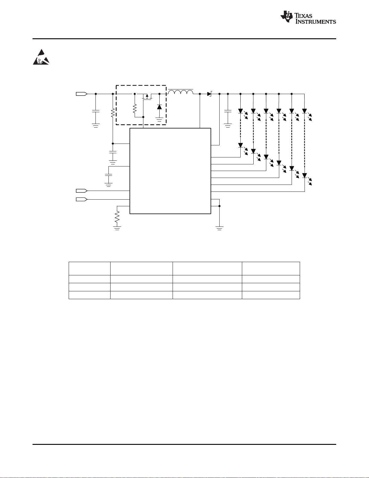
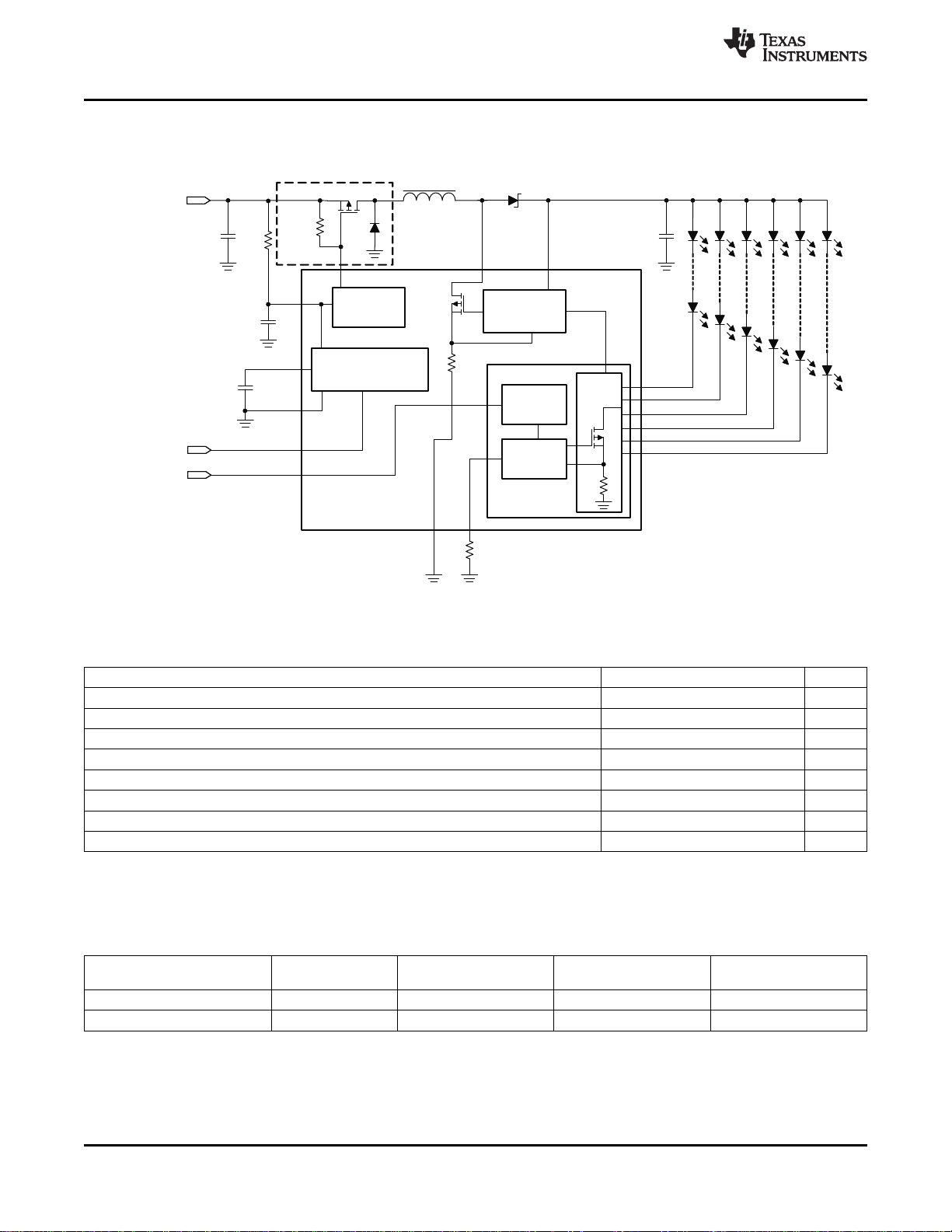
L1
10 Hm
Q1
D2
D1
C2
4.7 Fm
IFB1
IFB2
IFB3
IFB4
IFB5
IFB6
V
O
SWFault
V
BAT
Cin
EN
DCTRL
ISET
PGND
GND
R1
62kW
TPS61181/2
C4
0.1 Fm
Optional
5 Vto 24 V
C1
4.7 Fm
10 WLEDinseries,120 mA total
EN
PWMDimming
R2
51Ω
C3
1 Fm
R3
100kW
TPS61180/1/2
SLVS801E –DECEMBER 2007–REVISED APRIL 2013
This integrated circuit can be damaged by ESD. Texas Instruments recommends that all integrated circuits be handled with
appropriate precautions. Failure to observe proper handling and installation procedures can cause damage.
ESD damage can range from subtle performance degradation to complete device failure. Precision integrated circuits may be more
susceptible to damage because very small parametric changes could cause the device not to meet its published specifications.
www.ti.com
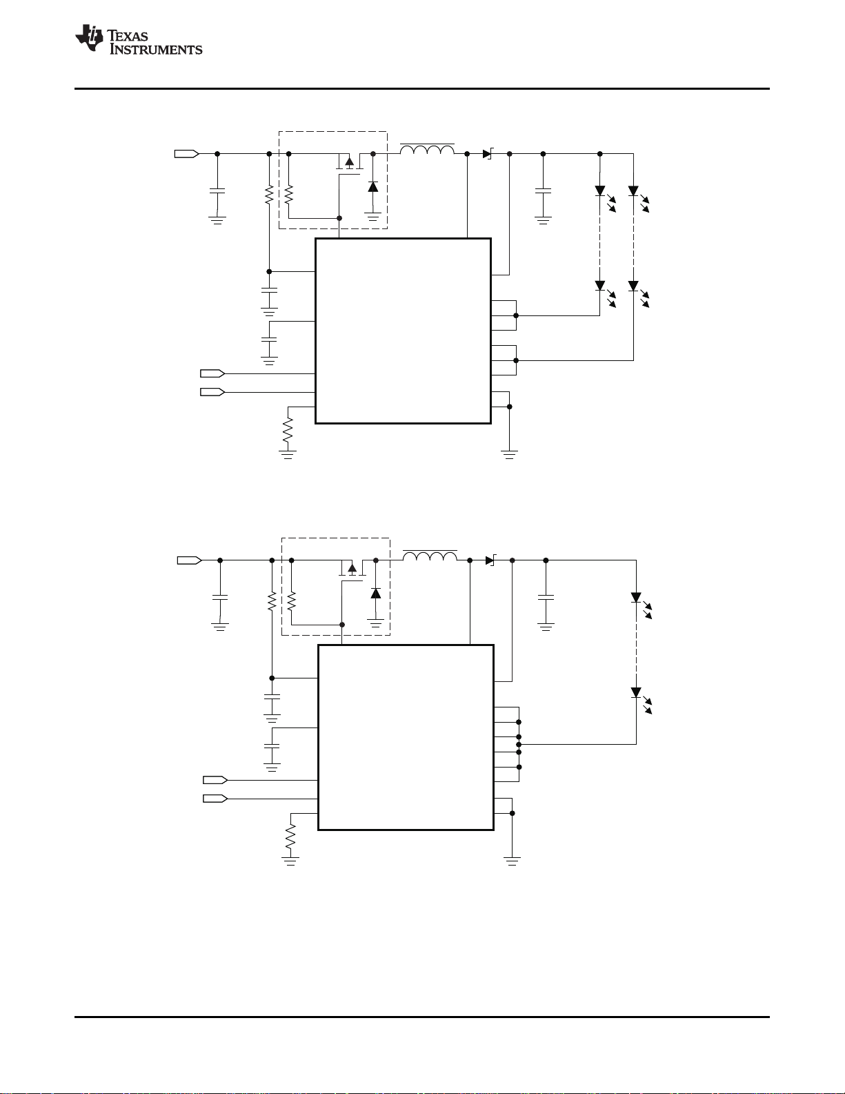
Figure 1. TPS61181/2 TYPICAL APPLICATION
ORDERING INFORMATION
PACKAGE IC SUPPLY SWITCHING FREQUENCY PACKAGE MARKING
TPS61180RTE External 3.3 V 1.0 MHz CCG
TPS61181RTE Built-in LDO 1.0 MHz CCH
TPS61182RTE Built-in LDO 1.3 MHz CCI
(1) For the most current package and ordering information, see the Package Option Addendum at the end
of this document, or see the TI website at www.ti.com.
2 Submit Documentation Feedback Copyright © 2007–2013, Texas Instruments Incorporated
Product Folder Links: TPS61180/1/2
(TYP)
(1)
DCTRL
IFB2
IFB1
IFB3
Cin
SW
V
O
5
EN
ISET
Fault
9
PGND
IFB5
13
1
GND
IFB6
IFB4
2
3
4
6
7 8
10
11
12
141516
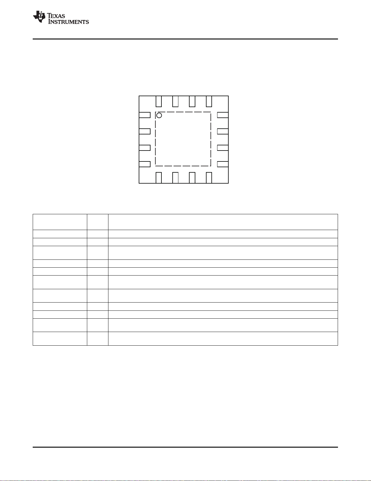
QFNPACKAGE
16Pin3x3
(TOP VIEW)
V
BAT
TPS61180/1/2
www.ti.com
SLVS801E –DECEMBER 2007–REVISED APRIL 2013
PINOUT
TERMINAL FUNCTIONS
TERMINAL I/O DESCRIPTION
NO. NAME
1 PGND I Power ground of the IC. Internally, it connects to the source of the PWM switch.
2 SW I This pin connects to the drain of the internal PWM switch, external Schottky diode and inductor.
3 V
4 V
5 ISET I The resistor on this pin programs the WLED output current.
6 Cin I Supply voltage of the IC. For TPS61181/2, it is the output of the internal LDO. Connect 0.1 μF bypass
7, 8, 9 IFB1-IFB3 I Current sink regulation inputs. They are connected to the cathode of WLEDs. The PWM loop regulates
12, 13, 14 IFB4-IFB6 the lowest V
10 GND I Signal ground of the IC.
11 DCTRL I Dimming control logic input. The dimming frequency range is 100 Hz to 1 kHz.
15 EN I The enable pin to the IC. For TPS61181/2, a logic high signal turns on the internal LDO and enables the
16 Fault I Gate driver output for an external PFET used for fault protection. It can also be used as signal output for
BAT
O
I This pin is connected to the battery supply. It provides the pull-up voltage for the Fault pin and battery
voltage signal. For TPS61181/2, this is also the input to the internal LDO.
O This pin monitors the output of the boost regulator. Connect this pin to the anode of the WLED strings.
capacitor to this pin. For TPS61180, connect an external 3.3 V supply to power the IC.
to 400 mV. Each channel is limited to 25 mA current.
IFB
IC. Therefore, do not connect the EN pin to the Cin pin.
system fault report.
Copyright © 2007–2013, Texas Instruments Incorporated Submit Documentation Feedback 3
Product Folder Links: TPS61180/1/2
C2
4.7 Fm
IFB1
IFB2
IFB3
IFB4
IFB5
IFB6
V
O
SW
PGND
GND
10 WLEDinseries,120 mA total
Current
Regulator
Dimming
Control
L1
10 Hm
Q1
D2
Cin
C4
0.1 Fm
Optional
CurrentMode
PWMControl
IFB 1...IFB 6
Fault
Protection
5 Vto 24 V
C1
4.7 Fm
R3
51 W
C3
1 Fm
InternalRegulator
(TPS61181/2only)
EN
PWMDimming
Fault
ISET
V
BAT
EN
DCTRL
D1
R1
R3
100kW
TPS61180/1/2
SLVS801E –DECEMBER 2007–REVISED APRIL 2013
FUNCTIONAL BLOCK DIAGRAM
www.ti.com
ABSOLUTE MAXIMUM RATINGS
(1)
VALUE UNIT
–0.3 to 24 V
–0.3 to 3.6 V
–0.3 to 40 V
–0.3 to 20 V
–0.3 to 7 V
over operating free-air temperature range (unless otherwise noted)
Voltages on pin V
Voltage on pin Cin
BAT
(2)
and Fault
Voltage on pin SW and V
Voltage on pin IFB1 to IFB6
Voltage on all other pins
Continuous power dissipation See Dissipation Rating Table
Operating junction temperature range –40 to 150 °C
Storage temperature range –65 to 150 °C
(1) Stresses beyond those listed under absolute maximum ratings may cause permanent damage to the device. These are stress ratings
only, and functional operation of the device at these or any other conditions beyond those indicated under recommended operating
conditions is not implied. Exposure to absolute-maximum-rated conditions for extended periods may affect device reliability.
(2) All voltage values are with respect to network ground terminal.
DISSIPATION RATINGS
TPS61180/1/2RTE
TPS61180/1/2RTE
(1) The JEDEC low-K (1s) board used to derive this data was a 3in×3in, two-layer board with 2-ounce copper traces on top of the board.
PACKAGE R
(2) The JEDEC high-K (2s2p) board used to derive this data was a 3in×3in, multilayer board with 1-ounce internal power and ground.
(2)
(2)
O
(2)
(2)
(1)
(2)
θJA
POWER RATING POWER RATING POWER RATING
TA≤ 25°C TA= 70°C TA= 85°C
270°C/W 370 mW 204 mW 148 mW
48.7°C/W 2.05 W 1.13 W 821 mW
4 Submit Documentation Feedback Copyright © 2007–2013, Texas Instruments Incorporated
Product Folder Links: TPS61180/1/2
TPS61180/1/2
www.ti.com
SLVS801E –DECEMBER 2007–REVISED APRIL 2013
RECOMMENDED OPERATING CONDITIONS
MIN TYP MAX UNIT
V
C
V
Battery input voltage range 5.0 24 V
bat
IC supply voltage range 2.7 3.6 V
in
Output voltage range Vin 38 V
O
L Inductor 4.7 10 μH
C
C
F
T
T
Input capacitor 1 μF
I
Output capacitor 2.2 10 μF
O
PWM dimming frequency 0.1 1 kHz
PWM
Operating ambient temperature –40 85 °C
A
Operating junction temperature –40 125 °C
J
ELECTRICAL CHARACTERISTICS
V
= 10.8 V, 0.1 μF at Cin, EN = Logic High, IFB current = 15m A, IFB voltage = 500 mV, TA= –40°C to 85°C, typical
BAT
values are at TA= 25°C (unless otherwise noted)
PARAMETER TEST CONDITIONS MIN TYP MAX UNIT
SUPPLY CURRENT
V
BAT
V
cc
V
cin
I
q_bat
I
q_Vcc
I
Q_sw
I
SD
V
cc_UVLO
V
bat_UVLO
V
bat_hys
EN AND DCTRL
V
H
V
L
R
PD
T
SD
CURRENT REGULATION
V
ISET
K
ISET
IFB Current accuracy Riset = 62K 19.4 20 20.6 mA
K
m
I
leak
I
IFB_MAX
BOOST OUTPUT REGULATION
V
IFB_L
V
IFB_H
V
reg_L
V
o_step
POWER SWITCH
R
PWM_SW
R
start
Battery input voltage range 5.0 24 V
IC supply voltage range TPS61180 only 2.7 3.15 3.6 V
Cin pin output voltage TPS61181/TPS61182 only 2.7 3.15 3.6 V
Operating quiescent current into V
BAT
Device enable, switching TPS61180 1
no load, Vin = 24 V
TPS61181/2 3
Operating quiescent current into Cin pin TPS61180 only 2 mA
Operating quiescent current into V
O
VO= 35V 50 μA
Shutdown current EN=GND 2 18 μA
Cin pin under-voltage lockout threshold TPS61180 only 2.2 2.4 V
V
under-voltage lockout threshold When Vin ramp down 4.2 4.5 V
BAT
V
under-voltage lockout hysteresis When Vin ramp up 300 mV
BAT
Logic high voltage 1.2 V
Logic low voltage 0.4 V
Pull down resistor on both pins 400 800 1600 kΩ
EN pulse width to shutdown EN high to low ms
TPS61180/1 27 37
TPS61182 21 28
ISET pin voltage 1.204 1.229 1.253 V
Current multiple Iout/ISET ISET current = 15 μA and 25 μA 970 1000 1030
(I
max–Imin
)/I
AVG
ISET current = 15 μA and 25 μA 1 2.5 %
IFB pin leakage current IFB voltage = 20 V on all pins 3 μA
Current sink max output current IFB = 425 mV 25 mA
VOdial up threshold Measured on V
VOdial down threshold Measured on V
(min) 400 mV
IFB
(min) 700 mV
IFB
Min Vout regulation voltage 16 V
VOstepping voltage 100 150 mV
PWM FET on-resistance VCC= 3.3 V for TPS61180 0.2 0.45 Ω
Start up charging resistance VO= 0 V 100 300 Ω
mA
Copyright © 2007–2013, Texas Instruments Incorporated Submit Documentation Feedback 5
Product Folder Links: TPS61180/1/2
TPS61180/1/2
SLVS801E –DECEMBER 2007–REVISED APRIL 2013
ELECTRICAL CHARACTERISTICS (continued)
V
= 10.8 V, 0.1 μF at Cin, EN = Logic High, IFB current = 15m A, IFB voltage = 500 mV, TA= –40°C to 85°C, typical
BAT
values are at TA= 25°C (unless otherwise noted)
PARAMETER TEST CONDITIONS MIN TYP MAX UNIT
V
start_r
I
LN_NFET
OSCILLATOR
f
S
D
max
D
min
OS, SC, OVP AND SS
I
LIM
V
ovp
V
ovp_IFB
V
sc
V
sc_dly
V
IFB_nouse
Fault OUTPUT
V
fault_high
V
fault_low
THERMAL SHUTDOWN
T
shutdown
T
hysteresis
Isolation FET start up threshold VIN–VO, VOramp up 1.2 2 V
PWM FET leakage current VSW= 35 V, TA= 25°C 1 μA
Oscillator frequency MHz
TPS61182 1.2 1.3 1.5
TPS61180/1 0.9 1.0 1.2
Maximum duty cycle IFB = 0 V 85 94 %
Minimum duty cycle %
N-Channel MOSFET current limit D = D
TPS61182 8
TPS61180/1 7
max
1.5 3 A
VOovervoltage threshold Measured on the VOpin 38 39 40 V
IFB overvoltage threshold Measured on the IFBx pin 15 17 20 V
Short circuit detection threshold VIN-VO, VOramp down 1.7 2.5 V
Short circuit detection delay during start up 32 ms
IFB no use detection threshold TPS61180 Only 0.6 V
Fault high voltage Measured as V
Fault low voltage Measured as V
= 15 V
bat–VFault
bat–VFault
, sink 0.1mA, Vin 6 8 10 V
0.1 V
Thermal shutdown threshold 160 °C
Thermal shutdown threshold hysteresis 15 °C
www.ti.com
6 Submit Documentation Feedback Copyright © 2007–2013, Texas Instruments Incorporated
Product Folder Links: TPS61180/1/2
80
82
84
86
88
90
92
94
96
98
100
0 25 50
75
100
125
150
I -OutputCurrent-mA
O
Efficiency-%
V =11V
bat
V =28.8V
O
V =17.6V
O
V =23.2V
O
80
82
84
86
88
90
92
94
96
98
100
Efficiency-%
0 25 50
75
100
125
150
I -OutputCurrent-mA
O
V =11V
bat
V =31.6V
O
V =36.2V
O
TPS61180/1/2
www.ti.com
SLVS801E –DECEMBER 2007–REVISED APRIL 2013
TYPICAL CHARACTERISTICS
Table of Graphs Figure
Load Efficiency TPS61181 V
Load Efficiency TPS61181 V
Load Efficiency TPS61181 V
Load Efficiency TPS61181 V
PWM Dimming Efficiency V
PWM Dimming Efficiency V
Dimming Linearity V
Dimming Linearity V
Output Ripple VO=28.8V; I
Switching Waveform V
Output Ripple at PWM Dimming V
Short Circuit Protection V
Open WLED Protection V
Startup Waveform V
EFFICIENCY EFFICIENCY
OUTPUT CURRENT OUTPUT CURRENT
vs vs
= 11V; VO=28.8V, 23.2V and 17.6V; L=4.7uH Figure 2
bat
= 11V; VO=36.2V and 31.6V; L=4.7uH Figure 3
bat
= 11V; VO=28.8V; L=4.7uH, L=10uH Figure 4
bat
= 7V, 11V and 19V; VO=28.8V; L=4.7uH Figure 5
bat
= 7V, 11V and 19V; VO=28.8V; I
bat
= 7V, 11V and 19V; VO=36.2V; I
bat
= 11V; VO=28.8V; I
bat
= 11V; VO=28.8V; I
bat
= 20μA; PWM Freq = 200Hz; Duty = 50% Figure 10
set
= 11V; I
bat
= 11V; I
bat
= 11V; I
bat
= 11V; I
bat
= 11V; I
bat
= 20μA Figure 11
set
= 20μA; PWM Freq = 200Hz; Duty = 50%; CO=4.7μF Figure 12
set
= 20μA Figure 13
set
= 20μA Figure 14
set
= 20μA Figure 15
set
= 20μA; PWM Freq = 1kHz Figure 8
set
= 20μA; PWM Freq = 200Hz Figure 9
set
= 20μA; PWM Freq = 200Hz Figure 6
set
= 20μA; PWM Freq = 200Hz Figure 7
set
Copyright © 2007–2013, Texas Instruments Incorporated Submit Documentation Feedback 7
Figure 2. Figure 3.
Product Folder Links: TPS61180/1/2
50
60
70
80
90
100
0 10 20 30 40 50 60 70 80 90 100
PWMDimmingDutyCycle-%
V =11V
bat
Efficiency-%
V =19V
bat
V =7V
bat
V =28.8V,TPS61181
ISET=20 A,
DimmingFrequency=200Hz
O
m
50
60
70
80
90
100
0 10 20 30 40 50 60 70 80 90 100
PWMDimmingDutyCycle-%
Efficiency-%
V =36.2V-TPS61181
ISET=20 A
DimmingFrequency=200Hz
O
m
V =19V
bat
V =11V
bat
V =7V
bat
80
82
84
86
88
90
92
94
96
98
100
Efficiency-%
0 25 50
75
100
125
150
I -OutputCurrent-mA
O
V =11V
bat
10 Hm
4.7 Hm
V =28.8V,
TPS61181
O
80
82
84
86
88
90
92
94
96
98
100
Efficiency-%
0 25 50
75
100
125
150
I -OutputCurrent-mA
O
V =7V
bat
V =19V
bat
V =11V
bat
V =28.8V,
TPS61181
O
TPS61180/1/2
SLVS801E –DECEMBER 2007–REVISED APRIL 2013
EFFICIENCY EFFICIENCY
OUTPUT CURRENT OUTPUT CURRENT
vs vs
Figure 4. Figure 5.
EFFICIENCY EFFICIENCY
DIMMING DUTY CYCLE DIMMING DUTY CYCLE
vs vs
www.ti.com
8 Submit Documentation Feedback Copyright © 2007–2013, Texas Instruments Incorporated
Figure 6. Figure 7.
Product Folder Links: TPS61180/1/2
50
100
150
200
250
300
350
5 7.5 12.5 15 17.5 20.0
OutputRipplePeaktoPeak-mV
10
V -V
bat
V =28.8V,TPS61181
ISET=20 A,
DimmingFrequency=200Hz
O
m
L =4.7 Hm
L =10 Hm
0
20
40
60
80
100
120
140
0 10 20 30 40 50 60 70 80 90 100
PWMDimmingDutyCycle-%
I -OutputCurrent-mA
O
TPS61181
ISET=20 A,
DimmingFrequency=200Hz
m
0
20
40
60
80
100
120
140
0 10 20 30 40 50 60 70 80 90 100
PWMDimmingDutyCycle-%
I -OutputCurrent-mA
O
TPS61181
ISET=20 A,
DimmingFrequency=1kHz
m
TPS61180/1/2
www.ti.com
SLVS801E –DECEMBER 2007–REVISED APRIL 2013
PWM DIMMING linearity 1kHz PWM DIMMING LINEARITY 200Hz
Figure 8. Figure 9.
PWM DIMMING OUTPUT RIPPLE CO=4.7μF
vs
INPUT VOLTAGE
Copyright © 2007–2013, Texas Instruments Incorporated Submit Documentation Feedback 9
Figure 10.
Product Folder Links: TPS61180/1/2

V
10V/div,DC
O
Inductor
Current
1 A/div,DC
t-Time-10 s/divm
EN
5V/div,DC
WLED
Current
20mA/div,DC
V
20V/div,DC
O
Inductor
Current
5 A/div,DC
Fault
5V/div,DC
t-Time-100 s/divm
Fault
5V/div,DC
V
20V/div,DC
O
Inductor
Current
1 A/div,DC
t-Time-1s/div
V
100mV/div, AC
bat
SW
20V/div,DC
V
100mV/div, AC
O
Inductor
Current
1 A/div,DC
t-Time-1 s/divm
V
100mV/div, AC
O
Inductor
Current
1 A/div,DC
t-Time-2 s/divm
DCTRL
5V/div,DC
TPS61180/1/2
SLVS801E –DECEMBER 2007–REVISED APRIL 2013
SWITCHING WAVEFORM OUTPUT RIPPLE AT PWM DIMMING CO=4.7μF
Figure 11. Figure 12.
OUTPUT SHORT PROTECTION OPEN WLED PROTECTION
www.ti.com
Figure 13. Figure 14.
STARTUP WAVEFORM
Figure 15.
10 Submit Documentation Feedback Copyright © 2007–2013, Texas Instruments Incorporated
Product Folder Links: TPS61180/1/2

TPS61180/1/2
www.ti.com
SLVS801E –DECEMBER 2007–REVISED APRIL 2013
DETAILED DESCRIPTION
Recently, WLEDs have gained popularity as an alternative to CCFL for backlighting media size LCD displays.
The advantages of WLEDs are power efficiency and low profile design. Due to the large number of WLEDs, they
are often arranged in series and parallel, and powered by a boost regulator with multiple current sink regulators.
Having more WLEDs in series reduces the number of parallel strings and therefore improves overall current
matching. However, the efficiency of the boost regulator declines due to the need for high output voltage. Also,
there have to be enough WLEDs in series to ensure the output voltage stays above the input voltage range.
Otherwise, a buck-boost (for example, SEPIC) power converter has to be adopted which could be more
expensive and complicated.
The TPS61180/1/2 family of ICs have integrated all the key function blocks to power and control up to 60
WLEDs. The devices include a 40V/1.5A boost regulator, six 25mA current sink regulators and protection circuit
for over-current, over-voltage and short circuit failures. The key advantages of the devices are small solution
size, low output AC ripple during PWM dimming control, and the capability to isolate the input and output during
fault conditions.
SUPPLY VOLTAGE
The TPS61181/2 ICs have built-in LDO linear regulator to supply the IC analog and logic circuit. The LDO is
powered up when the EN pin is high. The output of the LDO is connected to the Cin pin. A 0.1μF bypass
capacitor is required for LDO’s stable operation. Do not connect the Cin pin to the EN pin because this prevents
the IC from starting up. In addition, avoid connecting the Cin pin to any other circuit as this could introduce noise
into the IC supply voltage.
The TPS61180 has no built-in LDO linear regulator, and therefore requires an external supply voltage in the
range of 2.7V to 3.6V connected to the Cin pin. The benefit of using external supply is to reduce the power
losses incurred by the LDO as it provides the IC supply current. This loss could become a significant percentage
of total output power under light load condition. The Cin pin has 2.2V (typical) under-voltage lock out which turns
off the IC when the Cin pin voltage is below this threshold.
The voltage on the V
the input signal to the short circuit protection. For TPS61181/2 ICs, the V
LDO, and powers the IC. There is an under-voltage lockout on the V
voltage reduces to 4.2V (Typical). The IC restarts when the V
pin is the reference for the pull-up circuit of the Fault pin. In addition, it also serves as
BAT
pin voltage recovers by 300mV.
BAT
connects to the input of the internal
BAT
pin which disables the IC when its
BAT
BOOST REGULATOR
The boost regulator is controlled by current mode PWM, and loop compensation is integrated inside the IC. The
internal compensation ensures stable output over the full input and output voltage range. The TPS61180/1
switches at 1.0MHz, and the TPS61182 switches at 1.3MHz. The switching frequencies of the two devices,
including their tolerance, due not over-lap. Therefore, in the unlikely event that one device creates
electromagnetic inference to the system; the other device, switching at a different frequency, can provide an
alternative solution.
The output voltage of the boost regulator is automatically set by the IC to minimize the voltage drop across the
IFB pins. The IC automatically regulates the lowest IFB pin to 400mV, and consistently adjusts the boost output
voltage to account for any changes of the LED forward voltages.
When the output voltage is too close to the input, the boost regulator may not be able to regulate the output due
to the limitation of minimum duty cycle. In this case, increase the number of WLED in series or include series
ballast resistors in order to provide enough headroom for the boost operation.
The TPS61180/1/2 boost regulators cannot regulate their outputs to voltages below 15V.
Copyright © 2007–2013, Texas Instruments Incorporated Submit Documentation Feedback 11
Product Folder Links: TPS61180/1/2

IFB+ K
ISET
V
ISET
R
ISET
TPS61180/1/2
SLVS801E –DECEMBER 2007–REVISED APRIL 2013
www.ti.com
CURRENT PROGRAM AND PWM DIMMING
The six current sink regulators can each provide maximum 25mA. The IFB current must be programmed to
highest WLED current expected using the ISET pin resistor and the following Equation 1.
(1)
Where
K
= Current multiple (1000 typical)
ISET
V
= ISET pin voltage (1.229 V typical)
ISET
R
= ISET pin resistor
ISET
The TPS61180/1/2 ICs have built-in precise current sink regulator. The current matching among 6 current sinks
is below 2.5%. This means the differential value between the maximum and minimum current of the six current
sinks divided by the average current of the six is less than 2.5%.
The WLED brightness is controlled by the PWM signal on the DCTRL pin. The frequency and duty cycle of the
DCTRL signal is replicated on the IFB pin current. Keep the dimming frequency in the range of 100Hz to 1kHz to
avoid screen flickering and maintain dimming linearity. Screen flickering may occur if the dimming frequency is
below the range. The minimum achievable duty cycle increases with the dimming frequency. For example, while
a 0.1% dimming duty cycle, giving a 1000:1 dimming range, is achievable at 100 Hz dimming frequency, only 1%
duty cycle, giving a 100:1 dimming range, is achievable with a 1 KHz dimming frequency, and 5% dimming duty
cycle is achievable with 5KHz dimming frequency. The device could work at high dimming frequency like 20 KHz,
but only 15% duty cycle could be achievable. The TPS61180/1/2 ICs are designed to minimize the AC ripple on
the output capacitor during PWM dimming. Careful passive component selection is also critical to minimize AC
ripple on the output capacitor. See APPLICATION INFORMATION for more information.
ENABLE AND START UP
A logic high signal on the EN pin turns on the IC. For the TPS61181/2 ICs, taking EN high turns on the internal
LDO linear regulator which provides supply IC current. For all devices, an internal resistor R
resistor) is connected between the V
pin and VOpin to charge the output capacitor toward Vin. The Fault pin
BAT
(start up charging
start
outputs high during this time, and thus the external isolation PFET is turned off. Once the VOpin voltage is within
2 V (isolation FET start up threshold) of the V
of the PFET and connects the V
voltage to the boost regulator. This operation is to prevent the in-rush current
BAT
pin voltage, R
BAT
is open, and the Fault pin pulls down the gate
start
due to charging the output capacitor.
Once the isolation FET is turned on, the IC starts the PWM switching to raise the output voltage above V
BAT
Soft-start is implemented by gradually ramping up the reference voltage of the error amplifier to prevent voltage
over-shoot and in-rush current. See the start-up waveform of a typical example, Figure 15.
Pulling the EN pin low for 32ms (typical) shuts down the IC, resulting in the IC consuming less than 50μA in the
shutdown mode.
OVER-CURRENT, OVER-VOLTAGE AND SHORT-CIRCUIT PROTECTION
The TPS61180/1/2 family has pulse by pulse over-current limit of 1.5A (min). The PWM switch turns off when the
inductor current reaches this current threshold. The PWM switch remains off until the beginning of the next
switching cycle. This protects the IC and external component under over-load conditions. When there is
sustained over-current condition for more than 16ms ( under 100% dimming duty cycle), the IC turns off and
requires PER or the EN pin toggling to restart.
Under severe over-load and/or short circuit conditions, the VOpin can be pulled below the input (V
this condition, the current can follow directly from input to output through the inductor and Schottky diode.
Turning off the PWM switch alone does not limit current anymore. In this case, the TPS61180/1/2 ICs detect the
output voltage is 1V (short circuit detection threshold) below the input voltage, turns off the isolation FET, and
shuts down the IC. The IC restarts after input power-on reset (V
POR) or EN pin logic toggling.
BAT
During the IC start up, if there is short circuit condition on the boost converter output, the output capacitor will not
be charged to within 2V of V
shuts down and does not restart until there is V
through R
BAT
. After 32ms (short circuit detection delay during start up), the IC
start
POR or EN pin toggling. The isolation FET is never turned on
BAT
under the condition.
pin). Under
BAT
.
12 Submit Documentation Feedback Copyright © 2007–2013, Texas Instruments Incorporated
Product Folder Links: TPS61180/1/2

TPS61180/1/2
www.ti.com
SLVS801E –DECEMBER 2007–REVISED APRIL 2013
For the TPS61181/2 ICs, if one of the WLED strings is open, the boost output rises to over-voltage threshold
(39V typical). The IC detects the open WLED string by sensing no current in the corresponding IFB pin. As a
result, the IC removes the open IFB pin from the voltage feedback loop. Subsequently, the output voltage drops
down and is regulated to a voltage for the connected WLED strings. The IFB current of the connected WLED
string keeps in regulation during the whole transition. The IC only shuts down if it detects that all of the WLED
strings are open.
For the TPS61180, if the IC detects any open WLED string, the IC shuts down and remains off until there is V
BAT
POR or EN pin toggling.
For all the devices, if the over-voltage threshold is reached, but the current sensed on the IFB pin is below the
regulation target, the IC regulates the boost output at the over-voltage threshold. This operation could occur
when the WLED is turned on under cold temperature, and the forward voltages of the WLEDs exceed the overvoltage threshold. Maintaining the WLED current allows the WLED to warm up and their forward voltages to drop
below the over-voltage threshold.
For the TPS61181/2 ICs, if any IFB pin voltage exceeds IFB over-voltage threshold (17V typical), the IC turns off
the corresponding current sink and removes this IFB pin from VOregulation loop. The remaining IFB pins’ current
regulation is not affected. This condition often occurs when there are several shorted WLEDs in one string.
WLED mismatch typically does not create such large voltage difference among WLED strings.
For the TPS61180 IC, if any IFB pin voltage exceeds IFB over-voltage threshold, the IC shuts down and remains
off until there is V
POR or EN pin toggling.
BAT
IFB PIN UNUSED
If the application requires less than 6 WLED strings, one can easily disable unused IFB pins. The TPS61181/2
ICs simply require leaving the unused IFB pin open or shorting it to ground. If the IFB pin is open, the boost
output voltage ramps up to VOover-voltage threshold during start up. The IC then detects the zero current string,
and removes it from the feedback loop. If the IFB pin is shorted to ground, the IC detects the short immediately
after IC enable, and the boost output voltage does not go up to VOover-voltage threshold. Instead, it ramps to
the regulation voltage after soft start.
For the TPS61180, connect a 10 kΩ resistor from the unused IFB pin to ground. After the device is enabled, the
IC detects the resistor and disables the IFB pin from the feedback loop.
Copyright © 2007–2013, Texas Instruments Incorporated Submit Documentation Feedback 13
Product Folder Links: TPS61180/1/2

Ip+ I
dc
)
I
pp
2
I
pp
+
1
L
ǒ
1
V
O*Vbat
)
1
V
bat
Ǔ
F
S
I
dc
+
VO I
O
V
in
h
TPS61180/1/2
SLVS801E –DECEMBER 2007–REVISED APRIL 2013
www.ti.com
APPLICATION INFORMATION
INDUCTOR SELECTION
Because the selection of the inductor affects power supply’s steady state operation, transient behavior and loop
stability, the inductor is the most important component in switching power regulator design. There are three
specifications most important to the performance of the inductor, inductor value, DC resistance and saturation
current. The TPS61180/1/2 ICs are designed to work with inductor values between 4.7μH and 10μH. A 4.7μH
inductor could be available in a smaller or lower profile package, while 10μH may produce higher efficiency due
to lower inductor ripple. If the boost output current is limited by the over-current protection of the IC, using a
10μH inductor can offer higher output current.
The internal loop compensation for the PWM control is optimized for the recommended component values,
including typical tolerances. Inductor values can have ±20% tolerance with no current bias. When the inductor
current approaches saturation level, its inductance can decrease 20 to 35% from the 0A value depending on how
the inductor vendor defines saturation
In a boost regulator, the inductor DC current can be calculated as
(2)
Where
VO= boost output voltage
Io = boost output current
Vin= boost input voltage
η = power conversion efficiency, use 90% for TPS61180/1/2 applications
The inductor current peak to peak ripple can be calculated as
(3)
Where
Ipp= inductor peak to peak ripple
L = inductor value
Fs= Switching frequency
V
= boost input voltage
bat
Therefore, the peak current seen by the inductor is
(4)
Select the inductor with saturation current over the calculated peak current. To calculate the worse case inductor
peak current, use minimum input voltage, maximum output voltage and maximum load current.
Regulator efficiency is dependent on the resistance of its high current path, switching losses associated with the
PWM switch and power diode. Although the TPS61180/1/2 ICs have optimized the internal switch resistance, the
overall efficiency still relies on the DC resistance (DCR) of the inductor; lower DCR improves efficiency.
However, there is a trade off between DCR and inductor footprint. Furthermore, shielded inductors typically have
a higher DCR than unshielded ones. Table 1 lists recommended inductor models.
14 Submit Documentation Feedback Copyright © 2007–2013, Texas Instruments Incorporated
Product Folder Links: TPS61180/1/2

TPS61180/1/2
www.ti.com
SLVS801E –DECEMBER 2007–REVISED APRIL 2013
Table 1. Recommended Inductor for TPS61180/1/2
L DCR Typ I
(μH) (mΩ) (A) (LXWXH mm)
TOKO
A915AY-4R7M 4.7 38 1.87 5.2x5.2x3.0
A915AY-100M 10 75 1.24 5.2x5.2x3.0
TDK
SLF6028T-4R7M1R6 4.7 28.4 1.6 6.0x6.0x2.8
SLF6028T-100M1R3 10 53.2 1.3 6.0x6.0x2.8
sat
Size
OUTPUT CAPACITOR SELECTION
During PWM brightness dimming, the load transient causes voltage ripple on the output capacitor. Since the
PWM dimming frequency is in the audible frequency range, the ripple can produce audible noises on the output
ceramic capacitor. There are two ways to reduce or eliminate this audible noise. The first option is to select PWM
dimming frequency outside the audible range. This means the dimming frequency needs be to lower than 200Hz
or higher than 30KHz. The potential issue with low dimming frequency is that WLED on/off can become visible
and thus cause a flickering effect on the display. On the other hand, high dimming frequency can compromise
the dimming range since the LED current accuracy and current match are difficult to maintain at low dimming
duty cycle. The TPS61180/1/2 ICs can support minimum 1% dimming duty cycle up to 1KHz dimming frequency.
The second option is to reduce the amount of the output ripple, and therefore minimize the audible noise.
The TPS61180/1/2 ICs adopt a patented technology to limit output ripple even with small output capacitance. In
a typical application, the output ripple is less than 200mV during PWM dimming with 4.7μF output capacitor, and
the audible noise is not noticeable. The devices are designed to be stable with output capacitor down to 1.0μF.
However, the output ripple can increase with lower output capacitor.
Care must be taken when evaluating a ceramic capacitor’s derating due to applied dc voltage, aging and over
frequency. For example, larger form factor capacitors (in 1206 size) have their self resonant frequencies in the
switching frequency range of the TPS61180/1/2. So the effective capacitance is significantly lower. Therefore, it
may be necessary to use small capacitors in parallel instead of one large capacitor.
ISOLATION MOSFET SELECTION
The TPS61180/1/2 ICs provide a gate driver to an external P channel MOSFET which can be turned off during
device shutdown or fault condition. This MOSFET can provide a true shutdown function, and also protect the
battery from output short circuit conditions. The source of the PMOS should be connected to the input, and a pull
up resistor is required between the source and gate of the FET to keep the FET off during IC shutdown. To turn
on the isolation FET, the Fault pin is pulled low, and clamped at 8 V below the V
pin voltage.
BAT
During device shutdown or fault condition, the isolation FET is turned off, and the input voltage is applied on the
isolation MOSFET. During short circuit condition, the catch diode (D2 in typical application circuit) is forward
biased when the isolation FET is turned off. The drain of the isolation FET swings below ground. The voltage
cross the isolation FET can be momentarily greater than the input voltage. Therefore, select 30V PMOS for 24V
maximum input. The on resistor of the FET has large impact on power conversion efficiency since the FET
carries the input voltage. Select a MOSFET with R
less than 100mΩ to limit the power losses.
ds(on)
AUDIBLE NOISE REDUCTION
Ceramic capacitors can produce audible noise if the frequency of its AC voltage ripple is in the audible frequency
range. In TPS61180/1/2 applications, both input and output capacitors are subject to AC voltage ripple during
PWM brightness dimming. The ICs integrate a patented technology to minimize the ripple voltage, and thus
audible noises.
To further reduce the audible noise, one effective way is to use two or three small size capacitors in parallel
instead of one large capacitor. The application circuit in Figure 16 uses two 2.2-μF/25V ceramic capacitors at the
input and two 1-μF/50V ceramic capacitors at the output. All of the capacitors are in 0805 package. Although the
output ripple during PWM dimming is higher than one 4.7μF in a 1206 package, the overall audible noise is
lower.
Copyright © 2007–2013, Texas Instruments Incorporated Submit Documentation Feedback 15
Product Folder Links: TPS61180/1/2

C2
1 Fm
10 WLEDinseries, 120 mA total
C5
10 nF
C2a
L1
10 Hm
Q1
D2
D1
IFB1
IFB2
IFB3
IFB4
IFB5
IFB6
V
O
SWFault
V
BAT
Cin
EN
DCTRL
ISET
PGND
GND
R1
TPS61181/2
C4
0.1 Fm
Optional
5 Vto 24 V
C1a
EN
PWMDimming
R2
51Ω
C3
1 Fm
C1
2.2 Fm
C1, C1a: MurataGRM219R61E225K
C2, C2a: MurataGRM21BR71H105K
C3: MurataGRM21BR71H105K
C4: MurataGRM185R61A105K
C5: MurataGRM155R71H103K
L1: TOKO A915AY-100M
D1: VISHAY SS2P5-E3/84A
R3
100kW
2.2 Fm
1 Fm
TPS61180/1/2
SLVS801E –DECEMBER 2007–REVISED APRIL 2013
www.ti.com
In addition, connecting a 10-nF/50V ceramic capacitor between the VOpin and IFB1 pin can further reduce the
output AC ripple during the PWM dimming. Since this capacitor is subject to large AC ripple, choose a small
package such as 0402 to prevent it from producing noise.
LAYOUT CONSIDERATION
As for all switching power supplies, especially those providing high current and using high switching frequencies,
layout is an important design step. If layout is not carefully done, the regulator could show instability as well as
EMI problems. Therefore, use wide and short traces for high current paths. The input capacitor, C3 in the typical
application circuit, needs not only to be close to the V
pin, but also to the GND pin in order to reduce the input
BAT
ripple seen by the IC. The input capacitor, C1 in the typical application circuit, should be placed close to the
inductor. The SW pin carries high current with fast rising and falling edges. Therefore, the connection between
the pin to the inductor and Schottky should be kept as short and wide as possible. It is also beneficial to have the
ground of the output capacitor C2 close to the PGND pin since there is large ground return current flowing
between them. When laying out signal ground, it is recommended to use short traces separated from power
ground traces, and connect them together at a single point, for example on the thermal pad.
Thermal pad needs to be soldered on to the PCB and connected to the GND pin of the IC. Additional thermal via
can significantly improve power dissipation of the IC.
ADDITIONAL APPLICATION CIRCUITS
16 Submit Documentation Feedback Copyright © 2007–2013, Texas Instruments Incorporated
Figure 16. Audible Noise Reduction Circuit
Product Folder Links: TPS61180/1/2

L1
10 Hm
Q1
D2
D1
C2
4.7 Fm
IFB1
IFB2
IFB3
IFB4
IFB5
IFB6
V
O
SWFault
V
BAT
Cin
EN
DCTRL
ISET
PGND
GND
R1
62kW
TPS61180
C4
0.1uF
Optional
5 Vto 24V
C1
4.7 Fm
10 WLEDinseries, 120 mA total
EN
PWMDimming
3.3V
R2
51Ω
C3
1 Fm
R3
100kW
L1
10 Hm
Q1
D2
D1
C2
4.7 Fm
IFB1
IFB2
IFB3
IFB4
IFB5
IFB6
V
O
SWFault
V
BAT
Cin
EN
DCTRL
ISET
PGND
GND
R1
62kW
TPS61181/2
C4
0.1 Fm
Optional
5 Vto 24 V
C1
4.7 Fm
10 WLEDinseries,120 mA total
EN/PWM
R2
51Ω
C3
1 Fm
R3
100kW
TPS61180/1/2
www.ti.com
SLVS801E –DECEMBER 2007–REVISED APRIL 2013
Figure 17. Single Input Control Circuit
Copyright © 2007–2013, Texas Instruments Incorporated Submit Documentation Feedback 17
Figure 18. TPS61180 Typical Application
Product Folder Links: TPS61180/1/2

IFB1
IFB2
IFB3
IFB4
IFB5
IFB6
V
O
V
BAT
Cin
EN
DCTRL
ISET
PGND
GND
R1
62kW
TPS61181/2
C3
1 Fm
C4
0.1 Fm
EN
PWM
S0334-01
L1
10 Hm
D1
C2
4.7 Fm
SW
Fault
5 24VVto
C1
4.7 Fm
10WLEDsinSeries
40mA EachString
R2
51 W
R3
100kW
D2
Q1
Optional
L1
10 Hm
D1
C2
4.7 Fm
IFB1
IFB2
IFB3
IFB4
IFB5
IFB6
V
O
SW
Fault
V
BAT
Cin
EN
DCTRL
ISET
PGND
GND
R1
62kW
TPS61181/2
5 24VVto
C1
4.7 Fm
C3
1 Fm
C4
0.1 Fm
10WLEDsinSeries
20mA EachString
EN
R2
51 W
R3
100kW
D2
Q1
Optional
PWM
S0333-01
TPS61180/1/2
SLVS801E –DECEMBER 2007–REVISED APRIL 2013
www.ti.com
Figure 19. TSP61181/2 for Three Strings of LEDs
18 Submit Documentation Feedback Copyright © 2007–2013, Texas Instruments Incorporated
Figure 20. TSP61181/2 for Three Strings of LEDs with Double Current
Product Folder Links: TPS61180/1/2
IFB1
IFB2
IFB3
IFB4
IFB5
IFB6
V
O
V
BAT
Cin
EN
DCTRL
ISET
PGND
GND
R1
62kW
TPS61181/2
C3
1 Fm
C4
0.1 Fm
EN
PWM
10WLEDs120mA
S0336-01
High-BrightnessLED
L1
10 Hm
D1
C2
4.7 Fm
SW
Fault
5 24VVto
C1
4.7 Fm
R2
51 W
R3
100kW
D2
Q1
Optional
IFB1
IFB2
IFB3
IFB4
IFB5
IFB6
V
O
V
BAT
Cin
EN
DCTRL
ISET
PGND
GND
R1
51kW
TPS61181/2
C3
1 Fm
C4
0.1 Fm
EN
PWM
S0335-01
High-BrightnessLED
L1
10 Hm
D1
C2
4.7 Fm
SW
Fault
5 24VVto
C1
4.7 Fm
10WLEDsinSeries
72mA EachString
R2
51 W
R3
100kW
D2
Q1
Optional
TPS61180/1/2
www.ti.com
SLVS801E –DECEMBER 2007–REVISED APRIL 2013
Figure 21. TSP61181/2 for Two Strings High Brightness LEDs Application
Copyright © 2007–2013, Texas Instruments Incorporated Submit Documentation Feedback 19
Figure 22. TSP61181/2 for One String High Brightness LEDs Application
Product Folder Links: TPS61180/1/2

TPS61180/1/2
SLVS801E –DECEMBER 2007–REVISED APRIL 2013
www.ti.com
REVISION HISTORY
Changes from Revision C (April 2009) to Revision D Page
• Added to ELEC CHARA table, sub section POWER SWITCH: first row, TEST CONDITIONS Col: VCC= 3.3 V for
TPS61180 ............................................................................................................................................................................. 5
Changes from Revision D (February 2012) to Revision E Page
• Changed D
spec from 7% MAX to 8% for TPS61182 in Elec Char table. ....................................................................... 6
min
20 Submit Documentation Feedback Copyright © 2007–2013, Texas Instruments Incorporated
Product Folder Links: TPS61180/1/2

PACKAGE OPTION ADDENDUM
www.ti.com
PACKAGING INFORMATION
Orderable Device Status
TPS61180RTER ACTIVE WQFN RTE 16 3000 Green (RoHS
TPS61180RTERG4 ACTIVE WQFN RTE 16 3000 Green (RoHS
TPS61180RTET ACTIVE WQFN RTE 16 250 Green (RoHS
TPS61180RTETG4 ACTIVE WQFN RTE 16 250 Green (RoHS
TPS61181RTER ACTIVE WQFN RTE 16 3000 Green (RoHS
TPS61181RTERG4 ACTIVE WQFN RTE 16 3000 Green (RoHS
TPS61181RTET ACTIVE WQFN RTE 16 250 Green (RoHS
TPS61181RTETG4 ACTIVE WQFN RTE 16 250 Green (RoHS
TPS61182RTER ACTIVE WQFN RTE 16 3000 Green (RoHS
TPS61182RTERG4 ACTIVE WQFN RTE 16 3000 Green (RoHS
TPS61182RTET ACTIVE WQFN RTE 16 250 Green (RoHS
TPS61182RTETG4 ACTIVE WQFN RTE 16 250 Green (RoHS
(1)
The marketing status values are defined as follows:
ACTIVE: Product device recommended for new designs.
LIFEBUY: TI has announced that the device will be discontinued, and a lifetime-buy period is in effect.
NRND: Not recommended for new designs. Device is in production to support existing customers, but TI does not recommend using this part in a new design.
PREVIEW: Device has been announced but is not in production. Samples may or may not be available.
OBSOLETE: TI has discontinued the production of the device.
Package Type Package
(1)
Drawing
Pins Package
Qty
Eco Plan
(2)
& no Sb/Br)
& no Sb/Br)
& no Sb/Br)
& no Sb/Br)
& no Sb/Br)
& no Sb/Br)
& no Sb/Br)
& no Sb/Br)
& no Sb/Br)
& no Sb/Br)
& no Sb/Br)
& no Sb/Br)
Lead/Ball Finish MSL Peak Temp
(3)
Op Temp (°C) Top-Side Markings
CU NIPDAU Level-2-260C-1 YEAR -40 to 85 CCG
CU NIPDAU Level-2-260C-1 YEAR -40 to 85 CCG
CU NIPDAU Level-2-260C-1 YEAR -40 to 85 CCG
CU NIPDAU Level-2-260C-1 YEAR -40 to 85 CCG
CU NIPDAU Level-2-260C-1 YEAR -40 to 85 CCH
CU NIPDAU Level-2-260C-1 YEAR -40 to 85 CCH
CU NIPDAU Level-2-260C-1 YEAR -40 to 85 CCH
CU NIPDAU Level-2-260C-1 YEAR -40 to 85 CCH
CU NIPDAU Level-2-260C-1 YEAR -40 to 85 CCI
CU NIPDAU Level-2-260C-1 YEAR -40 to 85 CCI
CU NIPDAU Level-2-260C-1 YEAR -40 to 85 CCI
CU NIPDAU Level-2-260C-1 YEAR -40 to 85 CCI
(4)
(2)
Eco Plan - The planned eco-friendly classification: Pb-Free (RoHS), Pb-Free (RoHS Exempt), or Green (RoHS & no Sb/Br) - please check http://www.ti.com/productcontent for the latest availability
information and additional product content details.
TBD: The Pb-Free/Green conversion plan has not been defined.
11-Apr-2013
Samples
Addendum-Page 1

PACKAGE OPTION ADDENDUM
www.ti.com
Pb-Free (RoHS): TI's terms "Lead-Free" or "Pb-Free" mean semiconductor products that are compatible with the current RoHS requirements for all 6 substances, including the requirement that
lead not exceed 0.1% by weight in homogeneous materials. Where designed to be soldered at high temperatures, TI Pb-Free products are suitable for use in specified lead-free processes.
Pb-Free (RoHS Exempt): This component has a RoHS exemption for either 1) lead-based flip-chip solder bumps used between the die and package, or 2) lead-based die adhesive used between
the die and leadframe. The component is otherwise considered Pb-Free (RoHS compatible) as defined above.
Green (RoHS & no Sb/Br): TI defines "Green" to mean Pb-Free (RoHS compatible), and free of Bromine (Br) and Antimony (Sb) based flame retardants (Br or Sb do not exceed 0.1% by weight
in homogeneous material)
11-Apr-2013
(3)
MSL, Peak Temp. -- The Moisture Sensitivity Level rating according to the JEDEC industry standard classifications, and peak solder temperature.
(4)
Multiple Top-Side Markings will be inside parentheses. Only one Top-Side Marking contained in parentheses and separated by a "~" will appear on a device. If a line is indented then it is a
continuation of the previous line and the two combined represent the entire Top-Side Marking for that device.
Important Information and Disclaimer:The information provided on this page represents TI's knowledge and belief as of the date that it is provided. TI bases its knowledge and belief on information
provided by third parties, and makes no representation or warranty as to the accuracy of such information. Efforts are underway to better integrate information from third parties. TI has taken and
continues to take reasonable steps to provide representative and accurate information but may not have conducted destructive testing or chemical analysis on incoming materials and chemicals.
TI and TI suppliers consider certain information to be proprietary, and thus CAS numbers and other limited information may not be available for release.
In no event shall TI's liability arising out of such information exceed the total purchase price of the TI part(s) at issue in this document sold by TI to Customer on an annual basis.
Addendum-Page 2

PACKAGE MATERIALS INFORMATION
www.ti.com 1-Jan-2014
TAPE AND REEL INFORMATION
*All dimensions are nominal
Device Package
TPS61180RTER WQFN RTE 16 3000 330.0 12.4 3.3 3.3 1.1 8.0 12.0 Q2
TPS61180RTET WQFN RTE 16 250 180.0 12.4 3.3 3.3 1.1 8.0 12.0 Q2
TPS61181RTER WQFN RTE 16 3000 330.0 12.4 3.3 3.3 1.1 8.0 12.0 Q2
TPS61181RTET WQFN RTE 16 250 180.0 12.4 3.3 3.3 1.1 8.0 12.0 Q2
TPS61182RTER WQFN RTE 16 3000 330.0 12.4 3.3 3.3 1.1 8.0 12.0 Q2
Type
Package
Drawing
Pins SPQ Reel
Diameter
(mm)
Reel
Width
W1 (mm)
A0
(mm)B0(mm)K0(mm)P1(mm)W(mm)
Pin1
Quadrant
Pack Materials-Page 1

PACKAGE MATERIALS INFORMATION
www.ti.com 1-Jan-2014
*All dimensions are nominal
Device Package Type Package Drawing Pins SPQ Length (mm) Width (mm) Height (mm)
TPS61180RTER WQFN RTE 16 3000 367.0 367.0 35.0
TPS61180RTET WQFN RTE 16 250 210.0 185.0 35.0
TPS61181RTER WQFN RTE 16 3000 367.0 367.0 35.0
TPS61181RTET WQFN RTE 16 250 210.0 185.0 35.0
TPS61182RTER WQFN RTE 16 3000 367.0 367.0 35.0
Pack Materials-Page 2


IMPORTANT NOTICE
Texas Instruments Incorporated and its subsidiaries (TI) reserve the right to make corrections, enhancements, improvements and other
changes to its semiconductor products and services per JESD46, latest issue, and to discontinue any product or service per JESD48, latest
issue. Buyers should obtain the latest relevant information before placing orders and should verify that such information is current and
complete. All semiconductor products (also referred to herein as “components”) are sold subject to TI’s terms and conditions of sale
supplied at the time of order acknowledgment.
TI warrants performance of its components to the specifications applicable at the time of sale, in accordance with the warranty in TI’s terms
and conditions of sale of semiconductor products. Testing and other quality control techniques are used to the extent TI deems necessary
to support this warranty. Except where mandated by applicable law, testing of all parameters of each component is not necessarily
performed.
TI assumes no liability for applications assistance or the design of Buyers’ products. Buyers are responsible for their products and
applications using TI components. To minimize the risks associated with Buyers’ products and applications, Buyers should provide
adequate design and operating safeguards.
TI does not warrant or represent that any license, either express or implied, is granted under any patent right, copyright, mask work right, or
other intellectual property right relating to any combination, machine, or process in which TI components or services are used. Information
published by TI regarding third-party products or services does not constitute a license to use such products or services or a warranty or
endorsement thereof. Use of such information may require a license from a third party under the patents or other intellectual property of the
third party, or a license from TI under the patents or other intellectual property of TI.
Reproduction of significant portions of TI information in TI data books or data sheets is permissible only if reproduction is without alteration
and is accompanied by all associated warranties, conditions, limitations, and notices. TI is not responsible or liable for such altered
documentation. Information of third parties may be subject to additional restrictions.
Resale of TI components or services with statements different from or beyond the parameters stated by TI for that component or service
voids all express and any implied warranties for the associated TI component or service and is an unfair and deceptive business practice.
TI is not responsible or liable for any such statements.
Buyer acknowledges and agrees that it is solely responsible for compliance with all legal, regulatory and safety-related requirements
concerning its products, and any use of TI components in its applications, notwithstanding any applications-related information or support
that may be provided by TI. Buyer represents and agrees that it has all the necessary expertise to create and implement safeguards which
anticipate dangerous consequences of failures, monitor failures and their consequences, lessen the likelihood of failures that might cause
harm and take appropriate remedial actions. Buyer will fully indemnify TI and its representatives against any damages arising out of the use
of any TI components in safety-critical applications.
In some cases, TI components may be promoted specifically to facilitate safety-related applications. With such components, TI’s goal is to
help enable customers to design and create their own end-product solutions that meet applicable functional safety standards and
requirements. Nonetheless, such components are subject to these terms.
No TI components are authorized for use in FDA Class III (or similar life-critical medical equipment) unless authorized officers of the parties
have executed a special agreement specifically governing such use.
Only those TI components which TI has specifically designated as military grade or “enhanced plastic” are designed and intended for use in
military/aerospace applications or environments. Buyer acknowledges and agrees that any military or aerospace use of TI components
which have not been so designated is solely at the Buyer's risk, and that Buyer is solely responsible for compliance with all legal and
regulatory requirements in connection with such use.
TI has specifically designated certain components as meeting ISO/TS16949 requirements, mainly for automotive use. In any case of use of
non-designated products, TI will not be responsible for any failure to meet ISO/TS16949.
Products Applications
Audio www.ti.com/audio Automotive and Transportation www.ti.com/automotive
Amplifiers amplifier.ti.com Communications and Telecom www.ti.com/communications
Data Converters dataconverter.ti.com Computers and Peripherals www.ti.com/computers
DLP® Products www.dlp.com Consumer Electronics www.ti.com/consumer-apps
DSP dsp.ti.com Energy and Lighting www.ti.com/energy
Clocks and Timers www.ti.com/clocks Industrial www.ti.com/industrial
Interface interface.ti.com Medical www.ti.com/medical
Logic logic.ti.com Security www.ti.com/security
Power Mgmt power.ti.com Space, Avionics and Defense www.ti.com/space-avionics-defense
Microcontrollers microcontroller.ti.com Video and Imaging www.ti.com/video
RFID www.ti-rfid.com
OMAP Applications Processors www.ti.com/omap TI E2E Community e2e.ti.com
Wireless Connectivity www.ti.com/wirelessconnectivity
Mailing Address: Texas Instruments, Post Office Box 655303, Dallas, Texas 75265
Copyright © 2014, Texas Instruments Incorporated

 Loading...