

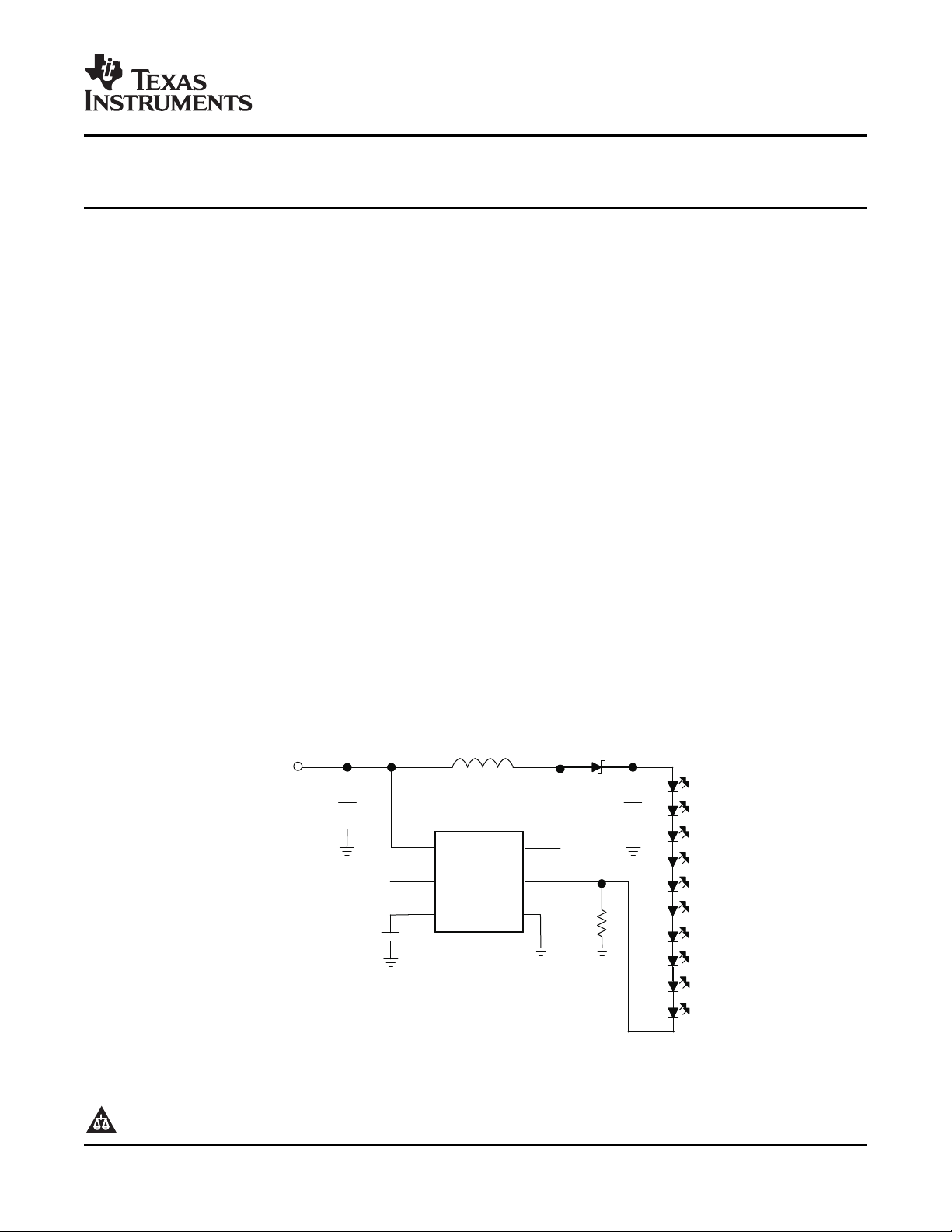
C1
D1
VIN SW
FB
GND
CTRL
COMP
C2
20mA
TPS61161
ON/OFF
DIMMING
CONTROL
V 3Vto18V
I
L1
22 Hm
1 Fm
C3
220nF
R
10
set
W
1 Fm
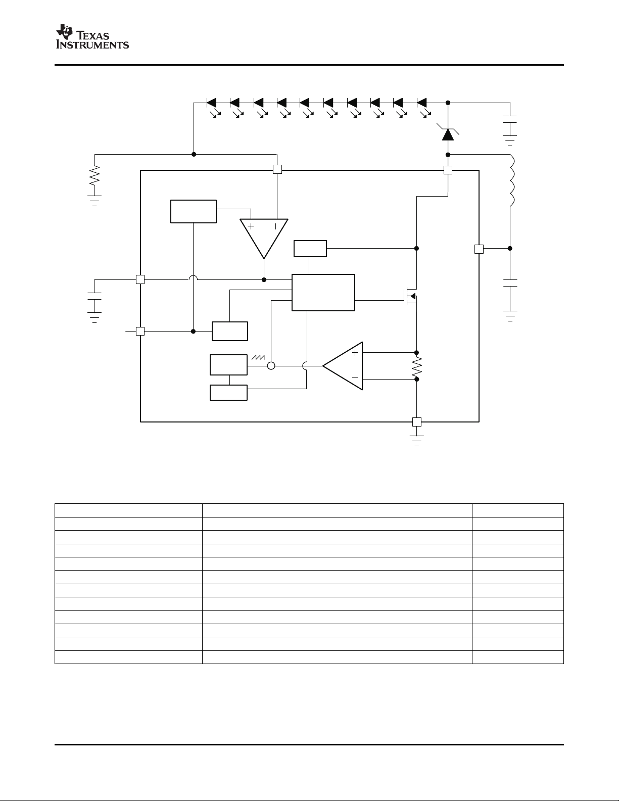
L1: TDKVLCF5020T-220MR75-1
C1:MurataGRM188R61E105K
C2: MurataGRM21BR71H105K
D1:ONsemiMBR0540T1
www.ti.com
White LED Driver With Digital and PWM Brightness Control in 2mm x 2mm
QFN Package for up to 10 LEDs in Series
1
FEATURES
• 2.7V to 18V Input Voltage Range
• 26V Open LED Protection for 6 LEDs
(TPS61160)
38V Open LED Protection for 10 LEDs
(TPS61161)
• 200mV Reference Voltage With ± 2% Accuracy
• Flexible Digital and PWM Brightness Control
• Built-in Soft Start
• Up to 90% Efficiency
• 2mm × 2mm × 0.8mm 6-pin QFN Package With
Thermal Pad
APPLICATIONS
• Cellular Phones
• Portable Media Players
• Ultra Mobile Devices
• GPS Receivers
• White LED Backlighting for Media Form Factor
Display
TPS61160
TPS61161
SLVS791 – NOVEMBER 2007
DESCRIPTION
With a 40-V rated integrated switch FET, the
TPS61160/1 is a boost converter that drives up to 10
LEDs in series. The boost converter runs at 600kHz
fixed switching frequency to reduce output ripple,
improve conversion efficiency, and allows for the use
of small external components.
The default white LED current is set with the external
sensor resistor Rset, and the feedback voltage is
regulated to 200mV, as shown in the typical
application. During the operation, the LED current can
be controlled using the 1 wire digital interface
(Easyscale™ protocol) through the CTRL pin.
Alternatively, a pulse width modulation (PWM) signal
can be applied to the CTRL pin through which the
duty cycle determines the feedback reference
voltage. In either digital or PWM mode, the
TPS61160/1 does not burst the LED current;
therefore, it does not generate audible noises on the
output capacitor. For maximum protection, the device
features integrated open LED protection that disables
the TPS61160/1 to prevent the output from exceeding
the absolute maximum ratings during open LED
conditions.
The TPS61160/1 is available in a space-saving,
2mm × 2mm QFN package with thermal pad.
1
Please be aware that an important notice concerning availability, standard warranty, and use in critical applications of
PRODUCTION DATA information is current as of publication date.
Products conform to specifications per the terms of the Texas
Instruments standard warranty. Production processing does not
necessarily include testing of all parameters.
Texas Instruments semiconductor products and disclaimers thereto appears at the end of this data sheet.
Figure 1. Typical Application of TPS61161
Copyright © 2007, Texas Instruments Incorporated
www.ti.com
TPS61160
TPS61161
SLVS791 – NOVEMBER 2007
These devices have limited built-in ESD protection. The leads should be shorted together or the device placed in conductive foam
during storage or handling to prevent electrostatic damage to the MOS gates.
(1)
(2)
PACKAGE MARKING
T
A
– 40 ° C to 85 ° C
ORDERING INFORMATION
OPEN LED PROTECTION PACKAGE
26V (typical) TPS61160DRV BZQ
38V (typical) TPS61161DRV BZR
(1) For the most current package and ordering information, see the TI Web site at www.ti.com .
(2) The DRV package is available in tape and reel. Add R suffix (TPS61160DRVR) to order quantities of 3000 parts per reel or add T suffix
(TPS61160DRVT) to order 250 parts per reel.
ABSOLUTE MAXIMUM RATINGS
over operating free-air temperature range (unless otherwise noted)
Supply Voltages on VIN
V
I
P
D
T
J
T
STG
Voltages on CTRL
Voltage on FB and COMP
Voltage on SW
(2)
Continuous Power Dissipation See Dissipation Rating Table
Operating Junction Temperature Range – 40 to 150 ° C
Storage Temperature Range – 65 to 150 ° C
(1) Stresses beyond those listed under absolute maximum ratings may cause permanent damage to the device. These are stress ratings
only, and functional operation of the device at these or any other conditions beyond those indicated under recommended operating
conditions is not implied. Exposure to absolute-maximum-rated conditions for extended periods may affect device reliability.
(2) All voltage values are with respect to network ground terminal.
(2)
(2)
(2)
(1)
VALUE UNIT
– 0.3 to 20 V
– 0.3 to 20 V
– 0.3 to 3 V
– 0.3 to 40 V
DISSIPATION RATINGS
BOARD PACKAGE R
(1)
Low-K
High-K
DRV 20 ° C/W 140 ° C/W 7.1 mW/ ° C 715 mW 395 mW 285 mW
(2)
DRV 20 ° C/W 65 ° C/W 15.4 mW/ ° C 1540 mW 845 mW 615 mW
θ JC
R
θ JA
(1) The JEDEC low-K (1s) board used to derive this data was a 3in × 3in, two-layer board with 2-ounce copper traces on top of the board.
(2) The JEDEC high-K (2s2p) board used to derive this data was a 3in × 3in, multilayer board with 1-ounce internal power and ground planes
and 2-ounce copper traces on top and bottom of the board.
DERATING FACTOR
ABOVE TA= 25 ° C
TA< 25 ° C TA= 70 ° C TA= 85 ° C
RECOMMENDED OPERATING CONDITIONS
MIN TYP MAX UNIT
V
V
L Inductor
f
C
C
T
T
(1) These values are recommended values that have been successfully tested in several applications. Other values may be acceptable in
Input voltage range, VIN 2.7 18 V
I
Output voltage range VIN 38 V
O
dim
IN
O
A
J
(1)
10 22 µ H
PWM dimming frequency 5 100 kHz
Input capacitor 1 µ F
Output capacitor
(1)
0.47 10 µ F
Operating ambient temperature – 40 85 ° C
Operating junction temperature – 40 125 ° C
other applications but should be fully tested by the user.
2 Submit Documentation Feedback Copyright © 2007, Texas Instruments Incorporated
Product Folder Link(s): TPS61160 TPS61161
www.ti.com
TPS61160
TPS61161
SLVS791 – NOVEMBER 2007
ELECTRICAL CHARACTERISTICS
VIN = 3.6 V, CTRL = VIN, TA= – 40 ° C to 85 ° C, typical values are at TA= 25 ° C (unless otherwise noted)
PARAMETER TEST CONDITIONS MIN TYP MAX UNIT
SUPPLY CURRENT
V
I
I
Q
I
SD
UVLO Undervoltage lockout threshold VIN falling 2.2 2.5 V
V
hys
ENABLE AND REFERENCE CONTROL
V
(CTRLh)
V
(CTRLl)
R
(CTRL)
t
off
t
es_det
t
es_delay
t
es_win
VOLTAGE AND CURRENT CONTROL
V
REF
V
(REF_PWM)
I
FB
f
S
D
max
t
min_on
I
sink
I
source
G
ea
R
ea
f
ea
POWER SWITCH
R
DS(on)
I
LN_NFET
OC and OLP
I
LIM
I
LIM_Start
t
Half_LIM
V
ovp
V
(FB_OVP)
t
REF
t
step
(1) To select EasyScale™ mode, the CTRL pin has to be low for more than t
Input voltage range, VIN 2.7 18 V
Operating quiescent current into VIN Device PWM switching no load 1.8 mA
Shutdown current CRTL=GND, VIN = 4.2 V 1 µ A
Undervoltage lockout hysterisis 70 mV
CTRL logic high voltage VIN = 2.7 V to 18 V 1.2 V
CTRL logic low voltage VIN = 2.7 V to 18 V 0.4 V
CTRL pull down resistor 400 800 1600 k Ω
CTRL pulse width to shutdown CTRL high to low 2.5 ms
Easy Scale detection time
(1)
CTRL pin low 260 µ s
Easy Scale detection delay 100 µ s
Easy Scale detection window time Measured from CTRL high 1 ms
Voltage feedback regulation voltage 196 200 204 mV
Voltage feedback regulation voltage under V
brightness control
Voltage feedback input bias current V
= 50 mV 47 50 53 mV
FB
V
= 20 mV 17 20 23
FB
= 200 mV 2 µ A
FB
Oscillator frequency 500 600 700 kHz
Maximum duty cycle V
= 100 mV 90% 93%
FB
Minimum on pulse width 40 ns
Comp pin sink current 100 µ A
Comp pin source current 100 µ A
Error amplifier transconductance 240 320 400 umho
Error amplifier output resistance 6 M Ω
Error amplifier crossover frequency 5 pF connected to COMP 500 kHz
N-channel MOSFET on-resistance VIN = 3.6 V 0.3 0.6
VIN = 3.0 V 0.7
N-channel leakage current V
N-Channel MOSFET current limit D = D
Start up current limit D = D
= 35 V, TA= 25 ° C 1 µ A
SW
max
max
0.56 0.7 0.84 A
0.4 A
Time step for half current limit 5 ms
Open LED protection threshold Measured on the SW pin, TPS61160 25 26 27 V
TPS61161 37 38 39
Open LED protection threshold on FB Measured on the FB pin, percentage
of Vref, Vref = 200 mV and 20 mV
V
filter time constant 180 µ s
REF
50%
VREF ramp up time 213 µ s
during t
es_det
es_win
Ω
Copyright © 2007, Texas Instruments Incorporated Submit Documentation Feedback 3
Product Folder Link(s): TPS61160 TPS61161
www.ti.com
VIN
CTRL
SW
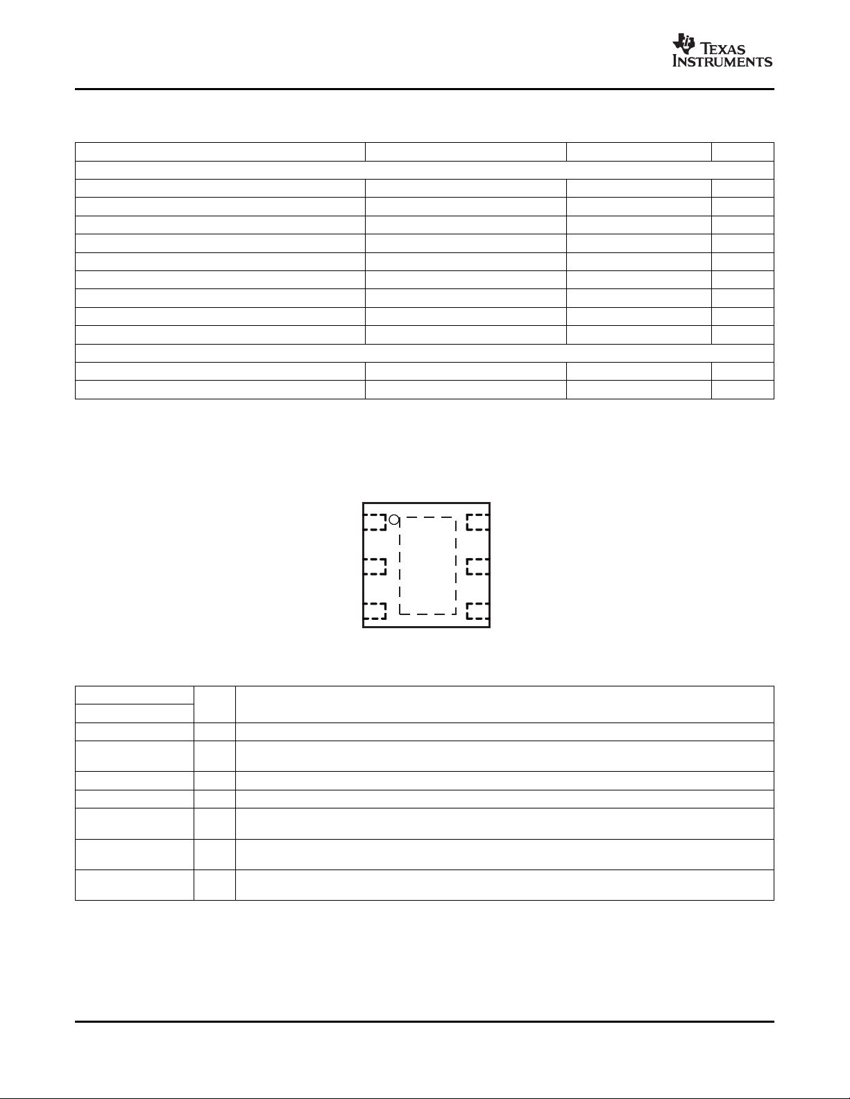
FB
COMP
GND
TOP VIEW
Thermal
Pad
6-PIN2mmx2mmx0.8mmQFN
TPS61160
TPS61161
SLVS791 – NOVEMBER 2007
ELECTRICAL CHARACTERISTICS (continued)
VIN = 3.6 V, CTRL = VIN, TA= – 40 ° C to 85 ° C, typical values are at TA= 25 ° C (unless otherwise noted)
PARAMETER TEST CONDITIONS MIN TYP MAX UNIT
EasyScale TIMING
t
start
t
EOS
t
H_LB
t
L_LB
t
H_HB
t
L_HB
V
ACKNL
t
valACKN
t
ACKN
THERMAL SHUTDOWN
T
shutdown
T
hysteresis
(2) Acknowledge condition active 0, this condition will only be applied in case the RFA bit is set. Open drain output, line needs to be pulled
high by the host with resistor load.
Start time of program stream 2 µ s
End time of program stream 2 360 µ s
High time low bit Logic 0 2 180 µ s
Low time low bit Logic 0 2 × t
High time high bit Logic 1 2 × t
H_LB
L_HB
360 µ s
360 µ s
Low time high bit Logic 1 2 180 µ s
Acknowledge output voltage low Open drain, Rpullup =15 k Ω to VIN 0.4 V
Acknowledge valid time See
Duration of acknowledge condition See
(2)
(2)
512 µ s
Thermal shutdown threshold 160 ° C
Thermal shutdown threshold hysteresis 15 ° C
2 µ s
DEVICE INFORMATION
TERMINAL FUNCTIONS
TERMINAL
NAME NO.
VIN 6 I The input supply pin for the IC. Connect VIN to a supply voltage between 2.7V and 18V.
SW 4 I
GND 3 O Ground
FB 1 I Feedback pin for current. Connect the sense resistor from FB to GND.
COMP 2 O
CTRL 5 I
Thermal Pad
I/O DESCRIPTION
This is the switching node of the IC. Connect the inductor between the VIN and SW pin. This pin is also
used to sense the output voltage for open LED protection
Output of the transconductance error amplifier. Connect an external capacitor to this pin to compensate the
regulator.
Control pin of the boost regulator. It is a multi-functional pin which can be used for enable control, PWM
and digital dimming.
The thermal pad should be soldered to the analog ground plane. If possible, use thermal via to connect to
ground plane for ideal power dissipation.
4 Submit Documentation Feedback Copyright © 2007, Texas Instruments Incorporated
Product Folder Link(s): TPS61160 TPS61161
www.ti.com
FUNCTIONAL BLOCK DIAGRAM
SW
Ramp
Generator
Oscillator
Current
Sensor
OLP
CTRL
GND
C3
L1
+
FB
Reference
Control
D1
Error
Amplifer
2
1
Rset
C2
Vin
C1
PWMControl
4
6
Soft
Start-up
5
3
COMP
TPS61160
TPS61161
SLVS791 – NOVEMBER 2007
TYPICAL CHARACTERISTICS
TABLE OF GRAPHS
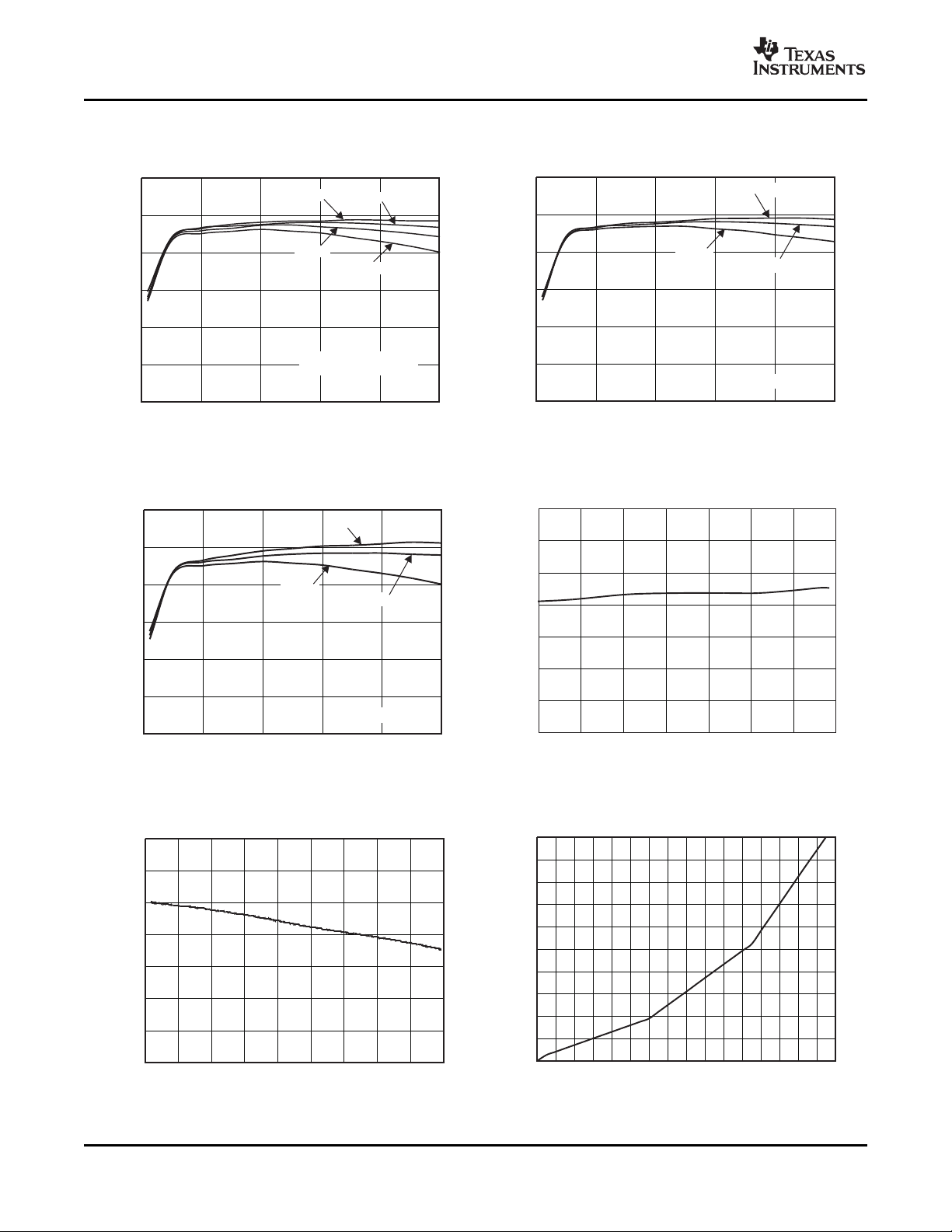
Efficiency TPS61160/1 VIN = 3.6 V; 4, 6, 8, 10 LEDs; L = 22 µ H Figure 2
Efficiency TPS61160 Figure 3
Efficiency TPS61161 Figure 4
= 20 mA; PWM Freq = 10 kHz Figure 9
LOAD
= 20 mA; L = 22 µ H Figure 10
LOAD
Product Folder Link(s): TPS61160 TPS61161
= 20 mA; L =22 µ H Figure 11
LOAD
= 20 mA; L = 22 µ H Figure 12
LOAD
Current limit TA= 25 ° C Figure 5
Current limit Figure 6
Easyscale step Figure 7
PWM dimming linearity VIN = 3.6 V; PWM Freq = 10 kHz and 40 kHz Figure 7
Output ripple at PWM dimming 8 LEDs; VIN = 3.6 V; I
Switching waveform 8 LEDs; VIN = 3.6 V; I
Start-up 8 LEDs; VIN = 3.6 V; I
Open LED protection 8 LEDs; VIN = 3.6 V; I
Copyright © 2007, Texas Instruments Incorporated Submit Documentation Feedback 5
FIGURE
www.ti.com
40
50
60
70
80
90
100
0 10 20 30 40 50
6LEDs- TPS61160
V =3.6V
I
V =3V
I
V =4.2V
I
OutputCurrent-mA
Efficiency-%
40
50
60
70
80
90
100
0 10 20 30 40 50
OutputCurrent-mA
4(12.8V),6(19.2V)LEDs
8(25.6V),10(32V)LEDs
6LEDs
V =3.6V
I
4LEDs
8LEDs
10LEDs
Efficiency-%
300
400
500
600
700
800
900
1000
20 30 40 50 60 70 80 90
DutyCycle-%
SwitchCurrentLimit-mA
40
50
60
70
80
90
100
0 10 20 30 40 50
10LEDs- TPS61161
V =5V
I
V =3.6V
I
V =12V
I
OutputCurrent-mA
Efficiency-%
300
400
500
600
700
800
900
1000
-40 -20 0 20 40 60 80 100 120 140
Temperature- C°
SwitchCurrentLimit-mA
0
20
40
60
80
100
120
140
160
180
200
0 2 4 6 8 10 12 14 16 18 20 22 24 26 28 30 32
EasyScaleStepStep
FBVoltage-mV
TPS61160
TPS61161
SLVS791 – NOVEMBER 2007
EFFICIENCY EFFICIENCY
vs vs
OUTPUT CURRENT OUTPUT CURRENT
Figure 2. Figure 3.
EFFICIENCY SWITCH CURRENT LIMIT
vs vs
OUTPUT CURRENT DUTY CYCLE
Figure 4. Figure 5.
SWITCH CURRENT LIMIT FB VOLTAGE
TEMPERATURE EASYSCALE STEP
6 Submit Documentation Feedback Copyright © 2007, Texas Instruments Incorporated
Figure 6. Figure 7.
vs vs
Product Folder Link(s): TPS61160 TPS61161
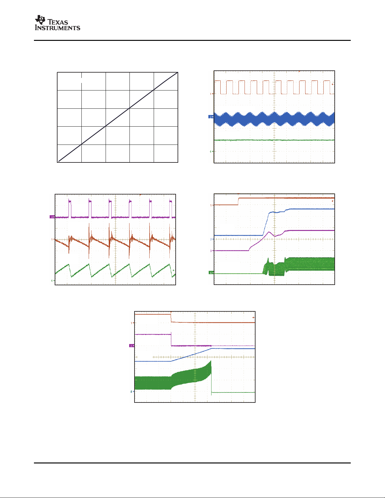
www.ti.com
t-100 s/divm
PWM2V/div
VOUT 20mV/div AC
I 10mA/div
LED
0
40
80
120
160
200
0 20 40 60 80 100
PWMDutyCycle-%
10kHz,40kHz
FBVoltage-mV
t-2ms/div
CTRL
5V/div
VOUT
10V/div
COMP
500mV/div
I
200mA/div
L
t-1 s/divm
SW
20V/div
VOUT
20mV/div
AC
I
200mA/div
L
t-100 s/divm
OPENLED
5V/div
FB
200mV/div
VOUT
10V/div
I
200mA/div
L
FB VOLTAGE
vs
PWM DUTY CYCLE OUTPUT RIPPLE at PWM DIMMING
Figure 8. Figure 9.
SWITCHING WAVEFORM START-UP
TPS61160
TPS61161
SLVS791 – NOVEMBER 2007
Figure 10. Figure 11.
Copyright © 2007, Texas Instruments Incorporated Submit Documentation Feedback 7
OPEN LED PROTECTION
Figure 12.
Product Folder Link(s): TPS61160 TPS61161

www.ti.com
I
LED
+
V
FB
R
SET
TPS61160
TPS61161
SLVS791 – NOVEMBER 2007
DETAILED DESCRIPTION
OPERATION
The TPS61160/1 is a high efficiency, high output voltage boost converter in small package size, The device is
ideal for driving up to 10 white LED in series. The serial LED connection provides even illumination by sourcing
the same output current through all LEDs, eliminating the need for expensive factory calibration. The device
integrates 40V/0.7A switch FET and operates in pulse width modulation (PWM) with 600kHz fixed switching
frequency. For operation see the block diagram. The duty cycle of the converter is set by the error amplifier
output and the current signal applied to the PWM control comparator. The control architecture is based on
traditional current-mode control; therefore, a slope compensation is added to the current signal to allow stable
operation for duty cycles larger than 50%. The feedback loop regulates the FB pin to a low reference voltage
(200mV typical), reducing the power dissipation in the current sense resistor.
SOFT START-UP
Soft-start circuitry is integrated into the IC to avoid a high inrush current during start-up. After the device is
enabled, the voltage at FB pin ramps up to the reference voltage in 32 steps, each step takes 213 µ s. This
ensures that the output voltage rises slowly to reduce the input current. Additionally, for the first 5msec after the
COMP voltage ramps, the current limit of the switch is set to half of the normal current limit spec. During this
period, the input current is kept below 400mA (typical). See the start-up waveform of a typical example,
Figure 11 .
OPEN LED PROTECTION
Open LED protection circuitry prevents IC damage as the result of white LED disconnection. The TPS61160/1
monitors the voltage at the SW pin and FB pin during each switching cycle. The circuitry turns off the switch FET
and shuts down the IC as soon as the SW voltage exceeds the Vovp threshold and the FB voltage is less than
half of regulation voltage for 8 clock cycles. As a result, the output voltage falls to the level of the input supply.
The device remains in shutdown mode until it is enabled by toggling the CTRL pin logic. To allow the use of
inexpensive low-voltage output capacitor, the TPS61160/1 has different open lamp protection thresholds to
prevent the internal 40V FET from breaking down. The threshold is set at 26V for the TPS61160 and 38V for the
TPS61161. The devices can be selected according to the number of external LEDs and their maximum forward
voltage.
SHUTDOWN
The TPS61160/1 enters shutdown mode when the CTRL voltage is logic low for more than 2.5ms. During
shutdown, the input supply current for the device is less than 1 µ A (max). Although the internal FET does not
switch in shutdown, there is still a DC current path between the input and the LEDs through the inductor and
Schottky diode. The minimum forward voltage of the LED array must exceed the maximum input voltage to
ensure that the LEDs remain off in shutdown. However, in the typical application with two or more LEDs, the
forward voltage is large enough to reverse bias the Schottky and keep leakage current low.
CURRENT PROGRAM
The FB voltage is regulated by a low 0.2V reference voltage. The LED current is programmed externally using a
current-sense resistor in series with the LED string. The value of the RSET is calculated using Equation 1 :
Where
I
= output current of LEDs
LED
V
= regulated voltage of FB
FB
R
= current sense resistor
SET
The output current tolerance depends on the FB accuracy and the current sensor resistor accuracy.
(1)
8 Submit Documentation Feedback Copyright © 2007, Texas Instruments Incorporated
Product Folder Link(s): TPS61160 TPS61161

www.ti.com
CTRL
low
high
FB
200mVxdutycycle
Insertbattery
CTRL
low
high
FB
Insertbattery
Programming
code
FBramp
Shutdowndelay
t
EnterESmode
Timingwindow
Programmingcode
50mV 50mV
EnterESmode
PWMsignal
Startup
delay
PWM
mode
Startupdelay
FBramp
Programmedvalue
(ifnotprogrammed, 200mVdefault )
Shutdown
delay
IC
Shutdown
Startupdelay
FBramp
ES
mode
ESdetectdelay
ESdetecttime
VFB+ Duty 200 mV
TPS61160
TPS61161
SLVS791 – NOVEMBER 2007
LED BRIGHTNESS DIMMING MODE SELECTION
The CTRL pin is used for the control input for both dimming modes, PWM dimming and 1 wire dimming. The
dimming mode for the TPS61160/1 is selected each time the device is enabled. The default dimming mode is
PWM dimming. To enter the 1 wire mode, the following digital pattern on the CTRL pin must be recognized by
the IC every time the IC starts from the shutdown mode.
1. Pull CTRL pin high to enable the TPS61160/1, and to start the 1 wire detection window.
2. After the EasyScale detection delay (t
detection time (t
es_detect
, 260 µ s).
3. The CTRL pin has to be low for more than EasyScale detection time before the EasyScale detection window
(t
, 1msec) expires. EasyScale detection window starts from the first CTRL pin low to high transition.
es_win
The IC immediately enters the 1 wire mode once the above 3 conditions are met. the EasyScale communication
can start before the detection window expires. Once the dimming mode is programmed, it can not be changed
without another start up. This means the IC needs to be shutdown by pulling the CTRL low for 2.5ms and
restarts. See the Dimming Mode Detection and Soft Start (Figure 13 ) for a graphical explanation.
, 100 µ s) expires, drive CTRL low for more than the EasyScale
es_delay
PWM BRIGHTNESS DIMMING
When the CTRL pin is constantly high, the FB voltage is regulated to 200mV typically. However, the CTRL pin
allows a PWM signal to reduce this regulation voltage; therefore, it achieves LED brightness dimming. The
relationship between the duty cycle and FB voltage is given by Equation 2 .
Where
Duty = duty cycle of the PWM signal
200 mV = internal reference voltage
As shown in Figure 14 , the IC chops up the internal 200mV reference voltage at the duty cycle of the PWM
signal. The pulse signal is then filtered by an internal low pass filter. The output of the filter is connected to the
error amplifier as the reference voltage for the FB pin regulation. Therefore, although a PWM signal is used for
brightness dimming, only the WLED DC current is modulated, which is often referred as analog dimming. This
eliminates the audible noise which often occurs when the LED current is pulsed in replica of the frequency and
duty cycle of PWM control. Unlike other scheme which filters the PWM signal for analog dimming, TPS61160/1
regulation voltage is independent of the PWM logic voltage level which often has large variations.
Copyright © 2007, Texas Instruments Incorporated Submit Documentation Feedback 9
Figure 13. Dimming Mode Detection and Soft Start PWM Brightness Dimming
Product Folder Link(s): TPS61160 TPS61161
(2)

www.ti.com
VBG
200mV
Error
Amplifier
FB
CTRL
TPS61160
TPS61161
SLVS791 – NOVEMBER 2007
For optimum performance, use the PWM dimming frequency in the range of 5kHz to 100kHz. The requirement of
minimum dimming frequency comes from the EasyScale detection delay and detection time specification in the
dimming mode selection. Since the CTRL pin is logic only pin, adding external RC filter applied to the pin does
not work.
Figure 14. Block Diagram of Programmable FB Voltage Using PWM Signal
To use lower PWM dimming, add an external RC network connected to the FB pin as shown in the additional
typical application (Figure 19 ).
DIGITAL 1 WIRE BRIGHTNESS DIMMING
The CTRL pin features a simple digital interface to allow digital brightness control. The digital dimming can save
the processor power and battery life as it does not require a PWM signal all the time, and the processor can
enter idle mode if available.
The TPS61160/1 adopts the EasyScale™ protocol for the digital dimming, which can program the FB voltage to
any of the 32 steps with single command. The step increment increases with the voltage to produce pseudo
logarithmic curve for the brightness step. See the Table 1 for the FB pin voltage steps. The default step is full
scale when the device is first enabled (V
= 200 mV). The programmed reference voltage is stored in an internal
FB
register. A power reset clears the register value and reset it to default.
EasyScale™: 1 WIRE DIGITAL DIMMING
EasyScale is a simple but flexible one pin interface to configure the FB voltage. The interface is based on a
master-slave structure, where the master is typically a microcontroller or application processor. Figure 15 and
Table 2 give an overview of the protocol. The protocol consists of a device specific address byte and a data byte.
The device specific address byte is fixed to 72 hex. The data byte consists of five bits for information, two
address bits, and the RFA bit. The RFA bit set to high indicates the Request for Acknowledge condition. The
Acknowledge condition is only applied if the protocol was received correctly. The advantage of EasyScale
compared with other on pin interfaces is that its bit detection is in a large extent independent from the bit
transmission rate. It can automatically detect bit rates between 1.7kBit/sec and up to 160kBit/sec.
Table 1. Selectable FB Voltage
FB voltage
(mV)
0 0 0 0 0 0 0
1 5 0 0 0 0 1
2 8 0 0 0 1 0
10 Submit Documentation Feedback Copyright © 2007, Texas Instruments Incorporated
3 11 0 0 0 1 1
4 14 0 0 1 0 0
5 17 0 0 1 0 1
6 20 0 0 1 1 0
7 23 0 0 1 1 1
8 26 0 1 0 0 0
D4 D3 D2 D1 D0
Product Folder Link(s): TPS61160 TPS61161

www.ti.com
DATA IN
Start
DATA OUT
ACK
RFA A1 A0 D4 D3 D2 D1 D0DA70DA61DA51DA41DA30DA20DA11DA0
0
Device Address
DATABYTE
EOS
Start
EOS
Start
Table 1. Selectable FB Voltage (continued)
FB voltage
(mV)
9 29 0 1 0 0 1
10 32 0 1 0 1 0
11 35 0 1 0 1 1
12 38 0 1 1 0 0
13 44 0 1 1 0 1
14 50 0 1 1 1 0
15 56 0 1 1 1 1
16 62 1 0 0 0 0
17 68 1 0 0 0 1
18 74 1 0 0 1 0
19 80 1 0 0 1 1
20 86 1 0 1 0 0
21 92 1 0 1 0 1
22 98 1 0 1 1 0
23 104 1 0 1 1 1
24 116 1 1 0 0 0
25 128 1 1 0 0 1
26 140 1 1 0 1 0
27 152 1 1 0 1 1
28 164 1 1 1 0 0
29 176 1 1 1 0 1
30 188 1 1 1 1 0
31 200 1 1 1 1 1
D4 D3 D2 D1 D0
TPS61160
TPS61161
SLVS791 – NOVEMBER 2007
Figure 15. EasyScale™ Protocol Overview
Table 2. EasyScale™ Bit Description
BYTE NAME DESCRIPTION
Device
Address
Byte
72 hex
Copyright © 2007, Texas Instruments Incorporated Submit Documentation Feedback 11
BIT TRANSMISSION
NUMBER DIRECTION
7 DA7 0 MSB device address
6 DA6 1
5 DA5 1
4 DA4 1
3 DA3 0
2 DA2 0
1 DA1 1
0 DA0 0 LSB device address
IN
Product Folder Link(s): TPS61160 TPS61161

www.ti.com
LowBit
(Logic0)
HighBit
(Logic1)
t
Low
t
HightLOW
t
High
EasyScaleTiming,withoutacknowledgeRFA =0
DA7
0
t
Start
StaticHigh StaticHigh
DATA IN
t
Start
T
EOS
T
EOS
DA0
0
RFA
0
D0
1
AddressByte DATA Byte
EasyScaleTiming,withacknowledgeRFA =1
StaticHigh
t
ACKN
Acknowledge
true,DataLine
pulleddownby
device
DATA IN
DATA OUT
Acknowledge
false,nopull
down
Controllerneedsto
PullupDataLineviaa
resistortodetect ACKN
ACKN
DA7
0
StaticHigh
T
EOS
t
valACK
DA0
0
RFA
1
D0
1
t
Start
t
Start
AddressByte DATA Byte
TPS61160
TPS61161
SLVS791 – NOVEMBER 2007
Table 2. EasyScale™ Bit Description (continued)
BYTE NAME DESCRIPTION
Data byte IN
BIT TRANSMISSION
NUMBER DIRECTION
7 (MSB) RFA Request for acknowledge. If high, acknowledge is applied by device
6 A1 0 Address bit 1
5 A0 0 Address bit 0
4 D4 Data bit 4
3 D3 Data bit 3
2 D2 Data bit 2
1 D1 Data bit 1
0 (LSB) D0 Data bit 0
Acknowledge condition active 0, this condition will only be applied in case RFA bit is
ACK OUT
set. Open drain output, Line needs to be pulled high by the host with a pullup
resistor. This feature can only be used if the master has an open drain output stage.
In case of a push pull output stage Acknowledge condition may not be requested!
Figure 16. EasyScale™ — Bit Coding
12 Submit Documentation Feedback Copyright © 2007, Texas Instruments Incorporated
Product Folder Link(s): TPS61160 TPS61161

www.ti.com
TPS61160
TPS61161
SLVS791 – NOVEMBER 2007
All bits are transmitted MSB first and LSB last. Figure 16 shows the protocol without acknowledge request (Bit
RFA = 0), Figure 16 with acknowledge (Bit RFA = 1) request. Prior to both bytes, device address byte and data
byte, a start condition must be applied. For this, the CTRL pin must be pulled high for at least t
the bit transmission starts with the falling edge. If the CTRL pin is already at high level, no start condition is
needed prior to the device address byte. The transmission of each byte is closed with an End of Stream
condition for at least t
(2 µ s).
EOS
The bit detection is based on a Logic Detection scheme, where the criterion is the relation between t
t
. It can be simplified to:
HIGH
High Bit: t
Low Bit: t
> t
< t
LOW
LOW
, but with t
, but with t
HIGH
HIGH
HIGH
at least 2x t
LOW
at least 2x t
, see Figure 16 .
LOW
, see Figure 16 .
HIGH
The bit detection starts with a falling edge on the CTRL pin and ends with the next falling edge. Depending on
the relation between t
and t
HIGH
, the logic 0 or 1 is detected.
LOW
The acknowledge condition is only applied if:
• Acknowledge is requested by a set RFA bit.
• The transmitted device address matches with the device address of the device.
• 16 bits is received correctly.
If the device turns on the internal ACKN-MOSFET and pulls the CTRL pin low for the time t
maximum then the Acknowledge condition is valid after an internal delay time t
ACKN-MOSFET is turned on after t
, when the last falling edge of the protocol was detected. The master
valACK
. This means that the internal
valACK
ACKN
controller keeps the line low in this period. The master device can detect the acknowledge condition with its input
by releasing the CTRL pin after t
and read back a logic 0. The CTRL pin can be used again after the
valACK
acknowledge condition ends.
Note that the acknowledge condition may only be requested in case the master device has an open drain output.
For a push-pull output stage, the use a series resistor in the CRTL line to limit the current to 500 µ A is
recommended to for such cases as:
• an accidentally requested acknowledge, or
• to protect the internal ACKN-MOSFET.
(2 µ s) before
start
LOW
, which is 512 µ s
and
UNDERVOLTAGE LOCKOUT
An undervoltage lockout prevents operation of the device at input voltages below typical 2.2V. When the input
voltage is below the undervoltage threshold, the device is shutdown and the internal switch FET is turned off. If
the input voltage rises by undervoltage lockout hysteresis, the IC restarts.
THERMAL SHUTDOWN
An internal thermal shutdown turns off the device when the typical junction temperature of 160 ° C is exceeded.
The device is released from shutdown automatically when the junction temperature decreases by 15 ° C.
Copyright © 2007, Texas Instruments Incorporated Submit Documentation Feedback 13
Product Folder Link(s): TPS61160 TPS61161

www.ti.com
ú
û
ù
ê
ë
é
+
-+
´´
=
)
V
1
VVV
1
(FL
1
I
ininfout
s
P
I
out_max
+
Vin ǒI
lim
* IPń2
Ǔ
h
Vout
I
in_DC
+
Vout Iout
Vin h
TPS61160
TPS61161
SLVS791 – NOVEMBER 2007
APPLICATION INFORMATION
MAXIMUM OUTPUT CURRENT
The overcurrent limit in a boost converter limits the maximum input current and thus maximum input power for a
given input voltage. Maximum output power is less than maximum input power due to power conversion losses.
Therefore, the current limit setting, input voltage, output voltage and efficiency can all change maximum current
output. The current limit clamps the peak inductor current; therefore, the ripple has to be subtracted to derive
maximum DC current. The ripple current is a function of switching frequency, inductor value and duty cycle. The
following equations take into account of all the above factors for maximum output current calculation.
Where:
Ip= inductor peak to peak ripple
L = inductor value
Vf= Schottky diode forward voltage
Fs = switching frequency
V
= output voltage of the boost converter. It is equal to the sum of VFB and the voltage drop across LEDs.
out
(3)
Where:
I
I
= maximum output current of the boost converter
out_max
= over current limit
lim
η = efficiency
For instance, when VIN is 3.0V, 8 LEDs output equivalent to VOUT of 26V, the inductor is 22 µ H, the Schottky
forward voltage is 0.2V; and then the maximum output current is 65mA in typical condition. When VIN is 5V, 10
LEDs output equivalent to VOUT of 32V, the inductor is 22 µ H, the Schottky forward voltage is 0.2V; and then the
maximum output current is 85mA in typical condition.
INDUCTOR SELECTION
The selection of the inductor affects steady state operation as well as transient behavior and loop stability. These
factors make it the most important component in power regulator design. There are three important inductor
specifications, inductor value, DC resistance and saturation current. Considering inductor value alone is not
enough.
The inductor value determines the inductor ripple current. Choose an inductor that can handle the necessary
peak current without saturating, according to half of the peak-to-peak ripple current given by Equation 3 , pause
the inductor DC current given by:
Inductor values can have ± 20% tolerance with no current bias. When the inductor current approaches saturation
level, its inductance can decrease 20% to 35% from the 0A value depending on how the inductor vendor defines
saturation current. Using an inductor with a smaller inductance value forces discontinuous PWM when the
inductor current ramps down to zero before the end of each switching cycle. This reduces the boost converter ’ s
maximum output current, causes large input voltage ripple and reduces efficiency. Large inductance value
provides much more output current and higher conversion efficiency. For these reasons, a 10 µ H to 22 µ H
inductor value range is recommended. A 22 µ H inductor optimized the efficiency for most application while
maintaining low inductor peak to peak ripple. Table 3 lists the recommended inductor for the TPS61160/1. When
recommending inductor value, the factory has considered – 40% and +20% tolerance from its nominal value.
(4)
(5)
14 Submit Documentation Feedback Copyright © 2007, Texas Instruments Incorporated
Product Folder Link(s): TPS61160 TPS61161

www.ti.com
C
out
+
ǒ
V
out
* V
in
Ǔ
I
out
V
out
Fs V
ripple
V
ripple_ESR
+ I
out
R
ESR
TPS61160
TPS61161
SLVS791 – NOVEMBER 2007
TPS61160/1 has built-in slope compensation to avoid sub-harmonic oscillation associated with current mode
control. If the inductor value is lower than 10 µ H, the slope compensation may not be adequate, and the loop can
be unstable. Therefore, customers need to verify the inductor in their application if it is different from the
recommended values.
Table 3. Recommended Inductors for TPS61160/1
PART NUMBER VENDOR
LQH3NPN100NM0 10 0.3 750 3 × 3 × 1.5 Murata
VLCF5020T-220MR75-1 22 0.4 750 5 × 5 × 2.0 TDK
CDH3809/SLD 10 0.3 570 4 × 4 × 1.0 Sumida
A997AS-220M 22 0.4 510 4 × 4 × 1.8 TOKO
SCHOTTKY DIODE SELECTION
The high switching frequency of the TPS61160/1 demands a high-speed rectification for optimum efficiency.
Ensure that the diode average and peak current rating exceeds the average output current and peak inductor
current. In addition, the diode ’ s reverse breakdown voltage must exceed the open LED protection voltage. The
ONSemi MBR0540 and the ZETEX ZHCS400 are recommended for TPS61160/1.
COMPENSATION CAPACITOR SELECTION
The compensation capacitor C3 (see the block diagram), connected from COMP pin to GND, is used to stabilize
the feedback loop of the TPS61160/1. Use 220nF ceramic capacitor for C3.
L DCR MAX SATURATION CURRENT SIZE
( µ H) ( Ω ) (mA) (L × W × H mm)
INPUT AND OUTPUT CAPACITOR SELECTION
The output capacitor is mainly selected to meet the requirements for the output ripple and loop stability. This
ripple voltage is related to the capacitor ’ s capacitance and its equivalent series resistance (ESR). Assuming a
capacitor with zero ESR, the minimum capacitance needed for a given ripple can be calculated by
where, V
using:
Due to its low ESR, Vripple_ESR can be neglected for ceramic capacitors, but must be considered if tantalum or
electrolytic capacitors are used.
Care must be taken when evaluating a ceramic capacitor ’ s derating under dc bias, aging and AC signal. For
example, larger form factor capacitors (in 1206 size) have a resonant frequencies in the range of the switching
frequency. So the effective capacitance is significantly lower. The DC bias can also significantly reduce
capacitance. Ceramic capacitors can loss as much as 50% of its capacitance at its rated voltage. Therefore,
leave the margin on the voltage rating to ensure adequate capacitance at the required output voltage.
The capacitor in the range of 1 µ F to 4.7 µ F is recommended for input side. The output requires a capacitor in the
range of 0.47 µ F to 10 µ F. The output capacitor affects the loop stability of the boost regulator. If the output
capacitor is below the range, the boost regulator can potentially become unstable. For example, if use the output
capacitor of 0.1 µ F, a 470nF compensation capacitor has to be used for the loop stable.
The popular vendors for high value ceramic capacitors are:
TDK (http://www.component.tdk.com/components.php )
Murata (http://www.murata.com/cap/index.html )
= peak-to-peak output ripple. The additional output ripple component caused by ESR is calculated
ripple
(6)
Copyright © 2007, Texas Instruments Incorporated Submit Documentation Feedback 15
Product Folder Link(s): TPS61160 TPS61161

www.ti.com
CTRL
GND
C3
L1
Rset
Vin
CTRL
SW
FB
COMP
GND
C1 Vin
C2
LEDsIN
LEDsOut
Minimizethe
areaofthis
trace
Placeenough
VIAsaround
thermalpadto
enhancethermal
performance
P
D(max)
+
125°C * T
A
RqJA
TPS61160
TPS61161
SLVS791 – NOVEMBER 2007
LAYOUT CONSIDERATIONS
As for all switching power supplies, especially those high frequency and high current ones, layout is an important
design step. If layout is not carefully done, the regulator could suffer from instability as well as noise problems.
To reduce switching losses, the SW pin rise and fall times are made as short as possible. To prevent radiation of
high frequency resonance problems, proper layout of the high frequency switching path is essential. Minimize the
length and area of all traces connected to the SW pin and always use a ground plane under the switching
regulator to minimize inter-plane coupling. The loop including the PWM switch, Schottky diode, and output
capacitor, contains high current rising and falling in nanosecond and should be kept as short as possible. The
input capacitor needs not only to be close to the VIN pin, but also to the GND pin in order to reduce the IC
supply ripple. Figure 17 shows a sample layout.
Figure 17. Sample Layout
THERMAL CONSIDERATIONS
The maximum IC junction temperature should be restricted to 125 ° C under normal operating conditions. This
restriction limits the power dissipation of the TPS61160/1. Calculate the maximum allowable dissipation, P
and keep the actual dissipation less than or equal to P
using Equation 7 :
where, T
junction-to-ambient given in Power Dissipation Table.
is the maximum ambient temperature for the application. R
A
The TPS61160/1 comes in a thermally enhanced QFN package. This package includes a thermal pad that
improves the thermal capabilities of the package. The R
layout and thermal pad connection. The thermal pad must be soldered to the analog ground on the PCB. Using
thermal vias underneath the thermal pad as illustrated in the layout example. Also see the QFN/SON PCB
Attachment application report (SLUA271 ).
16 Submit Documentation Feedback Copyright © 2007, Texas Instruments Incorporated
Product Folder Link(s): TPS61160 TPS61161
. The maximum-power-dissipation limit is determined
D(max)
of the QFN package greatly depends on the PCB
θ JA
θ JA
is the thermal resistance
,
D(max)
(7)

www.ti.com
ADDITIONAL TYPICAL APPLICATIONS
Vin3Vto5V
L1
10 Hm
C1
1 Fm
D1
Rset
10 W
VIN SW
FB
GND
CTRL
COMP
C2
0.47 Fm
20 mA
C3
220 nF
TPS61160
ON/ OFF
DIMMING
CONTROL
L1:
C1:MurataGRM188R61A105K
C2:MurataGRM188R61E474K
D1:
MurataLQH3NPN100NM0
ONsemiMBR0540T1
L1
10 Hm
C1
1 Fm
D1
Rset
10 W
VIN SW
FB
GND
CTRL
COMP
C2
0.47 Fm
220 nF
TPS61160
ON/OFF
DIMMING
CONTROL
80kW
10kW
100kW
0.1 Fm
C3
PWMSignal:1.8V;200Hz
LEDCurrent=1.8Vx(1-d)/(8xRset)
L1:
C1:MurataGRM188R61A105K
C2:MurataGRM188R61E474K
D1:
MurataLQH3NPN100NM0
ONsemiMBR0540T1
TPS61160
TPS61161
SLVS791 – NOVEMBER 2007
Figure 18. Li-Ion Driver for 6 White LEDs
Copyright © 2007, Texas Instruments Incorporated Submit Documentation Feedback 17
Figure 19. Li-Ion Driver for 6 White LEDs With External PWM Dimming Network
Product Folder Link(s): TPS61160 TPS61161

www.ti.com
Vin3Vto5V
L1
22 Hm
D1
Rset
10 W
VIN SW
FB
GND
CTRL
COMP
C2
1 Fm
20mA
C3
220nF
TPS61161
ON/OFF
DIMMING
CONTROL
C1
1 Fm
L1: TDKVLCF5020T-220MR75-1
C1:MurataGRM188R61A105K
C2: MurataGRM21BR71H105K
D1:ONsemiMBR0540T1
TPS61160
TPS61161
SLVS791 – NOVEMBER 2007
Figure 20. Li-Ion Driver for 8 White LEDs
18 Submit Documentation Feedback Copyright © 2007, Texas Instruments Incorporated
Product Folder Link(s): TPS61160 TPS61161

PACKAGE OPTION ADDENDUM
www.ti.com
20-Mar-2008
PACKAGING INFORMATION
Orderable Device Status
(1)
Package
Type
Package
Drawing
Pins Package
Qty
Eco Plan
TPS61160DRVR ACTIVE SON DRV 6 3000 Green (RoHS&
no Sb/Br)
TPS61160DRVRG4 ACTIVE SON DRV 6 3000 Green (RoHS &
no Sb/Br)
TPS61160DRVT ACTIVE SON DRV 6 250 Green (RoHS &
no Sb/Br)
TPS61160DRVTG4 ACTIVE SON DRV 6 250 Green (RoHS &
no Sb/Br)
TPS61161DRVR ACTIVE SON DRV 6 3000 Green (RoHS&
no Sb/Br)
TPS61161DRVRG4 ACTIVE SON DRV 6 3000 Green (RoHS &
no Sb/Br)
TPS61161DRVT ACTIVE SON DRV 6 250 Green (RoHS &
no Sb/Br)
TPS61161DRVTG4 ACTIVE SON DRV 6 250 Green (RoHS &
no Sb/Br)
(1)
The marketing status values are defined as follows:
ACTIVE: Product device recommended for new designs.
LIFEBUY: TI has announced that the device will be discontinued, and a lifetime-buy period is in effect.
NRND: Not recommended for new designs. Device is in production to support existing customers, but TI does not recommend using this part in
a new design.
PREVIEW: Device has been announced but is not in production. Samples may or may not be available.
OBSOLETE: TI has discontinued the production of the device.
(2)
Lead/Ball Finish MSL Peak Temp
CU NIPDAU Level-1-260C-UNLIM
CU NIPDAU Level-1-260C-UNLIM
CU NIPDAU Level-1-260C-UNLIM
CU NIPDAU Level-1-260C-UNLIM
CU NIPDAU Level-1-260C-UNLIM
CU NIPDAU Level-1-260C-UNLIM
CU NIPDAU Level-1-260C-UNLIM
CU NIPDAU Level-1-260C-UNLIM
(3)
(2)
Eco Plan - The planned eco-friendly classification: Pb-Free (RoHS), Pb-Free (RoHS Exempt), or Green (RoHS & no Sb/Br) - please check
http://www.ti.com/productcontent for the latest availability information and additional product content details.
TBD: The Pb-Free/Green conversion plan has not been defined.
Pb-Free (RoHS): TI's terms "Lead-Free" or "Pb-Free" mean semiconductor products that are compatible with the current RoHS requirements
for all 6 substances, including the requirement that lead not exceed 0.1% by weight in homogeneous materials. Where designed to be soldered
at high temperatures, TI Pb-Free products are suitable for use in specified lead-free processes.
Pb-Free (RoHS Exempt): This component has a RoHS exemption for either 1) lead-based flip-chip solder bumps used between the die and
package, or 2) lead-based die adhesive used between the die and leadframe. The component is otherwise considered Pb-Free (RoHS
compatible) as defined above.
Green (RoHS & no Sb/Br): TI defines "Green" to mean Pb-Free (RoHS compatible), and free of Bromine (Br) and Antimony (Sb) based flame
retardants (Br or Sb do not exceed 0.1% by weight in homogeneous material)
(3)
MSL, Peak Temp. -- The Moisture Sensitivity Level rating according to the JEDEC industry standard classifications, and peak solder
temperature.
Important Information and Disclaimer:The information provided on this page represents TI's knowledge and belief as of the date that it is
provided. TI bases its knowledge and belief on information provided by third parties, and makes no representation or warranty as to the
accuracy of such information. Efforts are underway to better integrate information from third parties. TI has taken and continues to take
reasonable steps to provide representative and accurate information but may not have conducted destructive testing or chemical analysis on
incoming materials and chemicals. TI and TI suppliers consider certain information to be proprietary, and thus CAS numbers and other limited
information may not be available for release.
In no event shall TI's liability arising out of such information exceed the total purchase price of the TI part(s) at issue in this document sold by TI
to Customer on an annual basis.
Addendum-Page 1

PACKAGE MATERIALS INFORMATION
www.ti.com
TAPE AND REEL INFORMATION
11-Apr-2008
*All dimensions are nominal
Device Package
Type
TPS61160DRVT SON DRV 6 250 180.0 12.4 2.2 2.2 1.1 8.0 12.0 Q2
TPS61161DRVT SON DRV 6 250 180.0 12.4 2.2 2.2 1.1 8.0 12.0 Q2
Package
Drawing
Pins SPQ Reel
Diameter
(mm)
Reel
Width
W1 (mm)
A0 (mm) B0 (mm) K0 (mm) P1
(mm)W(mm)
Pin1
Quadrant
Pack Materials-Page 1

PACKAGE MATERIALS INFORMATION
www.ti.com
11-Apr-2008
*All dimensions are nominal
Device Package Type Package Drawing Pins SPQ Length (mm) Width (mm) Height (mm)
TPS61160DRVT SON DRV 6 250 190.5 212.7 31.8
TPS61161DRVT SON DRV 6 250 190.5 212.7 31.8
Pack Materials-Page 2


IMPORTANT NOTICE
Texas Instruments Incorporated and its subsidiaries (TI) reserve the right to make corrections, modifications, enhancements, improvements,
and other changes to its products and services at any time and to discontinue any product or service without notice. Customers should
obtain the latest relevant information before placing orders and should verify that such information is current and complete. All products are
sold subject to TI’s terms and conditions of sale supplied at the time of order acknowledgment.
TI warrants performance of its hardware products to the specifications applicable at the time of sale in accordance with TI’s standard
warranty. Testing and other quality control techniques are used to the extent TI deems necessary to support this warranty. Except where
mandated by government requirements, testing of all parameters of each product is not necessarily performed.
TI assumes no liability for applications assistance or customer product design. Customers are responsible for their products and
applications using TI components. To minimize the risks associated with customer products and applications, customers should provide
adequate design and operating safeguards.
TI does not warrant or represent that any license, either express or implied, is granted under any TI patent right, copyright, mask work right,
or other TI intellectual property right relating to any combination, machine, or process in which TI products or services are used. Information
published by TI regarding third-party products or services does not constitute a license from TI to use such products or services or a
warranty or endorsement thereof. Use of such information may require a license from a third party under the patents or other intellectual
property of the third party, or a license from TI under the patents or other intellectual property of TI.
Reproduction of TI information in TI data books or data sheets is permissible only if reproduction is without alteration and is accompanied
by all associated warranties, conditions, limitations, and notices. Reproduction of this information with alteration is an unfair and deceptive
business practice. TI is not responsible or liable for such altered documentation. Information of third parties may be subject to additional
restrictions.
Resale of TI products or services with statements different from or beyond the parameters stated by TI for that product or service voids all
express and any implied warranties for the associated TI product or service and is an unfair and deceptive business practice. TI is not
responsible or liable for any such statements.
TI products are not authorized for use in safety-critical applications (such as life support) where a failure of the TI product would reasonably
be expected to cause severe personal injury or death, unless officers of the parties have executed an agreement specifically governing
such use. Buyers represent that they have all necessary expertise in the safety and regulatory ramifications of their applications, and
acknowledge and agree that they are solely responsible for all legal, regulatory and safety-related requirements concerning their products
and any use of TI products in such safety-critical applications, notwithstanding any applications-related information or support that may be
provided by TI. Further, Buyers must fully indemnify TI and its representatives against any damages arising out of the use of TI products in
such safety-critical applications.
TI products are neither designed nor intended for use in military/aerospace applications or environments unless the TI products are
specifically designated by TI as military-grade or "enhanced plastic." Only products designated by TI as military-grade meet military
specifications. Buyers acknowledge and agree that any such use of TI products which TI has not designated as military-grade is solely at
the Buyer's risk, and that they are solely responsible for compliance with all legal and regulatory requirements in connection with such use.
TI products are neither designed nor intended for use in automotive applications or environments unless the specific TI products are
designated by TI as compliant with ISO/TS 16949 requirements. Buyers acknowledge and agree that, if they use any non-designated
products in automotive applications, TI will not be responsible for any failure to meet such requirements.
Following are URLs where you can obtain information on other Texas Instruments products and application solutions:
Products Applications
Amplifiers amplifier.ti.com Audio www.ti.com/audio
Data Converters dataconverter.ti.com Automotive www.ti.com/automotive
DSP dsp.ti.com Broadband www.ti.com/broadband
Clocks and Timers www.ti.com/clocks Digital Control www.ti.com/digitalcontrol
Interface interface.ti.com Medical www.ti.com/medical
Logic logic.ti.com Military www.ti.com/military
Power Mgmt power.ti.com Optical Networking www.ti.com/opticalnetwork
Microcontrollers microcontroller.ti.com Security www.ti.com/security
RFID www.ti-rfid.com Telephony www.ti.com/telephony
RF/IF and ZigBee® Solutions www.ti.com/lprf Video & Imaging www.ti.com/video
Mailing Address: Texas Instruments, Post Office Box 655303, Dallas, Texas 75265
Copyright © 2008, Texas Instruments Incorporated
Wireless www.ti.com/wireless
 Loading...