

www.ti.com
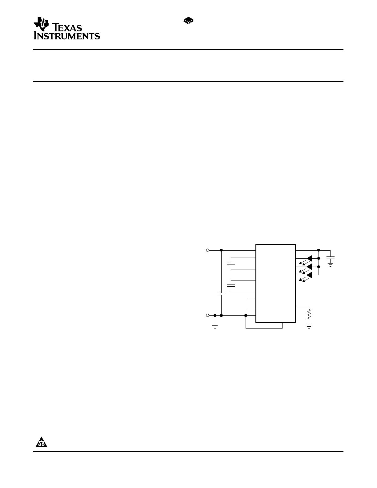
VIN
C1+
C1−
C2+
C2−
EN1
EN2
GND
PGND
VOUT
D1
D2
D3
ISET
0.47 F
0.47 F
1 F
1 F
VIN = 2.7 V
to 6.5 V
WHITE LED CHARGE PUMP CURRENT SOURCE
WITH PWM BRIGHTNESS CONTROL
FEATURES DESCRIPTION
• Regulated Output Current With 0.4%
Matching
• Drives up to 3 LEDs at 25 mA Each
• LED Brightness Control Through PWM
Control Signal
• High Efficiency by Fractional Conversion
With 1x and 1.5x Modes
• 1 MHz Switching Frequency
• 2.7 V to 6.5 V Operating Input Voltage Range
• Internal Softstart Limits Inrush Current
• Low Input Ripple and Low EMI
• Overcurrent and Overtemperature Protected
• Undervoltage Lockout With Hysteresis
• Ultra-Small 3mm x 3mm QFN Package
APPLICATIONS
• White LED Backlight for Color Displays in
Cellular Phones, Smart Phones, PDAs,
Handheld PCs, Digital Cameras, and
Camcorders
• Keypad Backlight
TPS60231
SLVS544 – OCTOBER 2004
The TPS60231 charge pump is optimized for white
LED supplies in color display backlight applications.
The device provides a constant current for each LED,
which the initial value can be set by an external
resistor. The supply voltage ranges from 2.7 V to
6.5 V and is ideally suited for all applications powered
by a single LI-Ion battery cell or three to four NiCd,
NiMH, or alkaline battery cells. Over an input voltage
range from 3.1 V to 6.5 V, the device provides a high
output current of up to 25 mA per LED with a total of
75 mA. High efficiency is achieved by utilizing a
1x/1.5x fractional conversion technique in combination with very low dropout current sources. In
addition, the current controlled charge pump ensures
low input current ripple and EMI. Only two external
1 µF and two 0.47 µF capacitors are required to build
a complete small and low cost power supply solution.
To reduce board space to a minimum, the device
switches at 1 MHz operating frequency and is available in a small 16-pin QFN (RGT) package.
PRODUCTION DATA information is current as of publication date.
Products conform to specifications per the terms of the Texas
Instruments standard warranty. Production processing does not
necessarily include testing of all parameters.
Please be aware that an important notice concerning availability, standard warranty, and use in critical applications of Texas
Instruments semiconductor products and disclaimers thereto appears at the end of this data sheet.
Copyright © 2004, Texas Instruments Incorporated
www.ti.com
TPS60231
SLVS544 – OCTOBER 2004
This integrated circuit can be damaged by ESD. Texas Instruments recommends that all integrated
circuits be handled with appropriate precautions. Failure to observe proper handling and installation
procedures can cause damage.
ESD damage can range from subtle performance degradation to complete device failure. Precision
integrated circuits may be more susceptible to damage because very small parametric changes could
cause the device not to meet its published specifications.
ORDERING INFORMATION
PACKAGED DEVICE
TPS60231RGTR QFN BKH
(1) T indicates shipment in tape and reel on a mini reel with 250 units
per reel.
(2) R indicates shipment in tape and reel with 3000 units per reel.
ABSOLUTE MAXIMUM RATINGS
over operating free-air temperature range (unless otherwise noted)
V
Supply voltage –0.3 V to 7 V
I
Voltage at EN1, EN2, VOUT, ISET –0.3 V to V
Output current at VOUT 150 mA
T
Maximum junction temperature 150 ° C
J
T
Operating free-air temperature –40 ° C to 85 ° C
A
T
Storage temperature –65 ° C to 150 ° C
st
Lead temperature 1,6 mm (1/16 inch) from case for 10 seconds 300 ° C
(1) Stresses beyond those listed under "absolute maximum ratings" may cause permanent damage to the device. These are stress ratings
only, and functional operation of the device at these or any other conditions beyond those indicated under "recommended operating
conditions" is not implied. Exposure to absolute-maximum-rated conditions for extended periods may affect device reliability.
(1) (2)
PACKAGE MARKING
(1)
UNIT
I
DISSIPATION RATINGS
PACKAGE
16-Pin QFN (RGT) 1.9 W 20 mW/ ° C 1 W 760 mW
(1) The thermal resistance junction to ambient of the QFN package is 52 ° C/W.
(1)
TA≤ 25 ° C DERATING FACTOR TA= 70 °C TA= 85 °C
POWER RATING ABOVE TA= 25 ° C POWER RATING POWER RATING
RECOMMENDED OPERATING CONDITIONS
MIN TYP MAX UNIT
Supply voltage at VIN 2.7 6.5 V
Maximum output current at VOUT 75 mA
C
Input capacitor 1 µF
i
C
Output capacitor 0.47 1 µF
o
Flying capacitor, C1, C2 0.22 0.47 µF
Operating junction temperature -40 125 °C
2

www.ti.com
TPS60231
SLVS544 – OCTOBER 2004
ELECTRICAL CHARACTERISTICS
VI= 3.6 V, EN1 = EN2 = VI, TA= -40 °C to 85 °C (unless otherwise noted)
PARAMETER TEST CONDITIONS MIN TYP MAX UNIT
SUPPLY VOLTAGE AND CURRENT
V
I
Q
I
SD
CHARGE PUMP STAGE
V
f Switching frequency 0.75 1 1.25 MHz
η Efficiency VI= 3.7 V, I
CURRENT SINKS
I
Dx
I
Dx
V
Iset Recommended ISET pin current range 4 130 µA
K IDxto ISET current ratio EN2 = EN1 = 1, ISET = 80 µA 230 260 280
V
ENABLE 1, ENABLE 2
V
V
I
IKG
I
IKG
V
Input voltage range IO= 0 mA to 75 mA 2.7 6.5 V
I
Operating quiescent current
VI= 4.2 V, x1-mode, EN1 = EN2 = 1, ISET = 20 µA 200 µA
IO= 0 mA, x1.5-mode 2.1 mA
Shutdown current EN2 = EN1 = GND 0.1 1 µA
Overvoltage limit LED1 unconnected, VI= 4.2 V 5.5 V
OUT
Startup time CO= 1 µF, IDX≥ 0.9 IDX, set 375 µs
Softstart duration 160 µs
= 15 mA each, V
LED
= 3.1 V 83%
DX
Shutdown temperature Temperature rising 160 ° C
Shutdown temperature hysteresis 20 ° C
Input current limit EN2 = EN1 = 1, ISET = 100 µA 350 mA
Recommended maximum current per cur- 3.2 V ≤ VI≤ 6.5 V 25 mA
rent sink
Current into each current sink when ISET 50 mA
is shorted to GND
Current matching between any two outputs V
Line regulation
3.0 V ≤ VI≤ 6.5 V, ISET shorted to GND
= 3.1 V, TA= 25 ° C –2% 0.4% 2%
Dx
3.2 V ≤ VI≤ 6.5 V, V
ISET = 80 µA
= 3.1 V, EN1 = EN2 = 1, ± 3%
Dx
EN2 = 0, EN1 = 1 200
Reference voltage for current set EN2 = 1, EN1 = 0 400 mV
ISET
EN2 = 1, EN1 = 1 580 600 620
EN2 = 0, EN1 = 1 200
Voltage at Dx to GND EN2 = 1, EN1 = 0 300 mV
source
EN2 = 1, EN1 = 1 400
EN1, EN2 high level input voltage 1.3 V
IH
EN1, EN2 low level input voltage 0.3 V
IL
EN1, EN2 trip point hysteresis 50 mV
EN2 input leakage current EN1, EN2 = GND or EN2 = VI, VI= 6.5 V 0.01 1 µA
EN1 input leakage current EN1 = VI, VI= 4.2 V 11 15 µA
Undervoltage lockout threshold Input voltage falling 2.1 V
(UVLO)
Undervoltage lockout hysteresis 50 mV
Frequency range at PWM 0 50 kHz
Recommended ON-time for PWM signal 2.5 µs
Shutdown delay time 0.5 0.85 1.5 ms
Delay time when EN1 = EN2 go to GND after which
the TPS60231 shuts down completely
3
www.ti.com
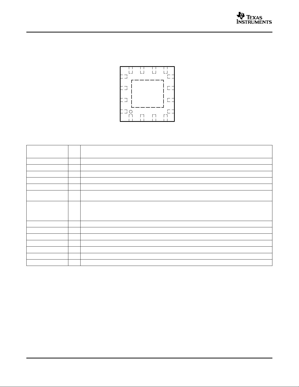
C2−
C1−
C1+
C2+
PGND
VIN
EN1
D2
D1
VOUT
GND
NC
NC
D3
31 2
7
5
6
8
12 11 10
9
15
13
14
16
EN2
4
QFN PACKAGE
(TOP VIEW)
TPS60231
SLVS544 – OCTOBER 2004
PIN ASSIGNMENT
Terminal Functions
TERMINAL
NAME NO.
C1+ 10 – Connect to the flying capacitor C1
C1– 11 – Connect to the flying capacitor C1
C2+ 9 – Connect to the flying capacitor C2
C2– 12 – Connect to the flying capacitor C2
D1-D3 6-4 I Current sink input. Connect the cathode of the white LEDs to these inputs.
EN1 15 I
EN2 16 I
GND 14 – Analog ground
ISET 1 I Connect a resistor between this pin and GND to set the maximum current through the LEDs.
NC 2, 3 – No internal connection
PGND 7 – Power ground
VIN 13 I Supply voltage input
VOUT 8 0 Connect the output capacitor and the anode of the LEDs to this pin.
Power PAD – – Connect with PGND and GND
I/O DESCRIPTION
Enable input. A logic high enables the converter, logic low forces the device into shutdown mode reducing
the supply current to less than 1 µA if EN2 is tied to GND.
An applied PWM signal reduces the LED current as a function of the duty cycle of the PWM signal. EN1 and
EN2 can be tied together for PWM dimming between 0 mA and the maximum set with ISET. EN1 and EN2
can also be used for digital dimming with 4 steps from 0 mA to the maximum current set with ISET. See the
application section for more details.
4
www.ti.com
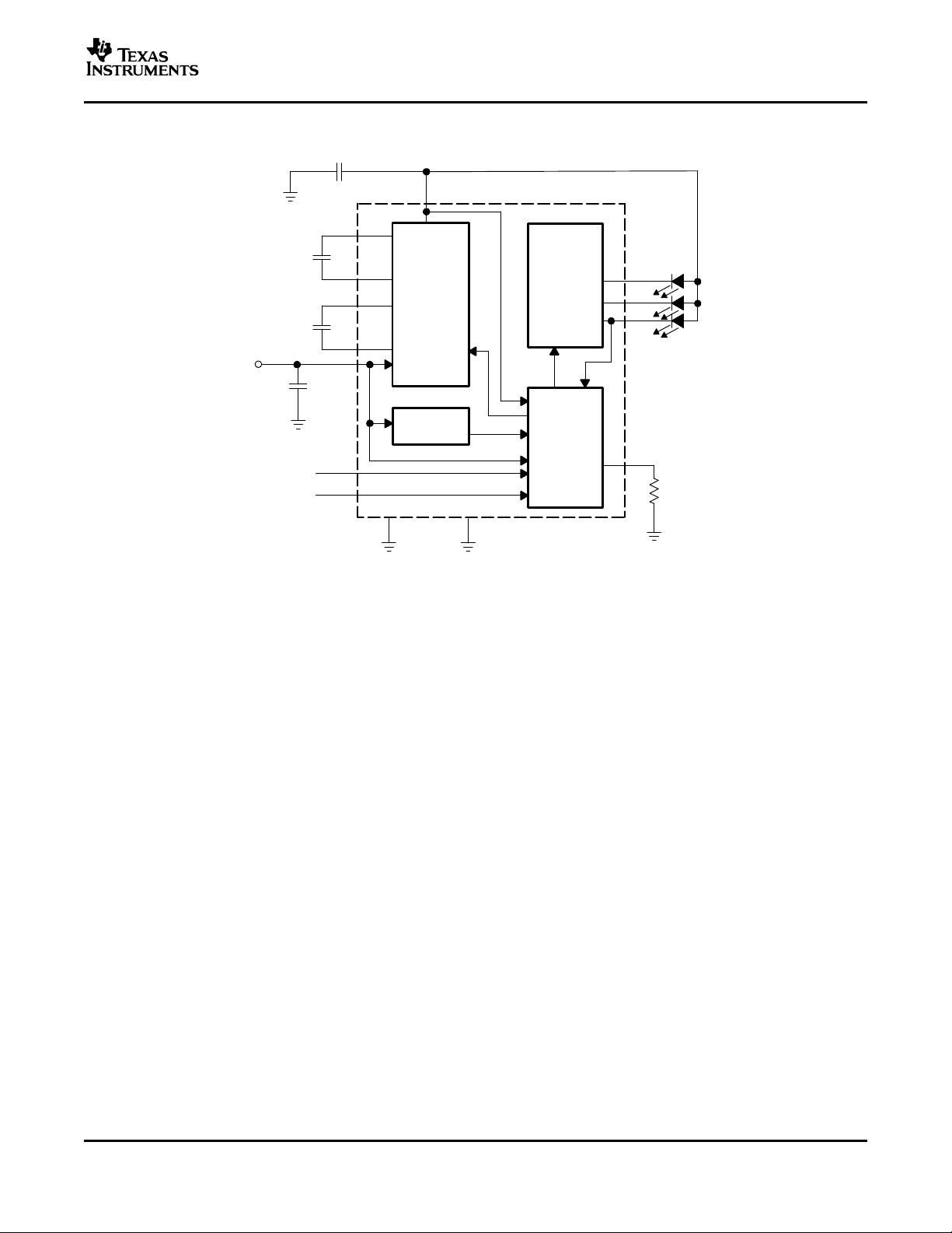
D3
D2
D1
C1+
C1−
C2+
C2−
EN2
VOUT
ISET
GND
EN1
Control
R
SET
VIN
Reference
0.47 F
0.47 F
1 F
Charge
Pump
Current
Sinks
1 F
PGND
FUNCTIONAL BLOCK DIAGRAM
TPS60231
SLVS544 – OCTOBER 2004
5
www.ti.com
0
10
20
30
40
50
60
70
80
90
100
2.7 3.1 3.5 3.9 4.3 4.7 5.1 5.5 5.9 6.3
I
LED
= 25 mA
VI − Input Voltage − V
Efficiency − %
I
LED
= 15 mA
I
LED
= 10 mA
I
LED
= 5 mA
0
10
20
30
40
50
60
70
80
90
100
2.7 3.1
3.5 3.9 4.3 4.7 5.1 5.5
5.9 6.3
VI − Input Voltage − V
Efficiency − %
I
LED
= 25 mA
I
LED
= 10 mA
I
LED
= 15 mA
I
LED
= 5 mA
TPS60231
SLVS544 – OCTOBER 2004
TYPICAL CHARACTERISTICS
Table of Graphs
vs Input voltage (I
EN2 = 0, EN1 = 1
η Efficiency
vs Input voltage (I
1, EN1 = 0
vs Input voltage (I
EN2 = EN1 = 1
IQQuiescent current vs Input voltage (T
Maximum output current from charge pump
stage
vs Input voltage (T
fsSwitching frequency vs Free-Air Temperature (T
LED current, I
Line transient response
LED
vs Duty cycle on PWM (I
For f = 32 kHz and f = 1 kHz, DC = 1% to 100%, VI= 3.6 V
VIand ID1vs time on scope, LED current at D1 with 8
VI= 4.2 V to 3.6 V to 4.2 V with EN2 = EN1 = 11, 3 x 20 mA
PWM signal and current at D1 vs time on scope 9, 10
Dimming response f = 32 kHz and f = 1 kHz, VI= 3.6 V, duty cycle = 50%,
EN1 = EN2 = PWM
Startup timing
VI= 3.6 V, 3 x 20 mA, EN1 = EN2 = 00 changed to 11
EN2 = EN1 = 11
= 25 mA, 15 mA, 10 mA, 5 mA per LED),
LED
= 25 mA, 15 mA, 10 mA, 5 mA per LED), EN2 = 2
LED
= 25 mA, 15 mA, 10 mA, 5 mA per LED), 3
LED
= –40 ° C, 25 ° C, 85 ° C) (measured with ID1= 5 mA) 4
A
= –40 ° C, 25 ° C, 85 ° C) 5
A
= -40 ° C to 85 ° C, VI= 3.6 V) 6
A
max set to 20 mA) 7
LED
FIGURE
1
EFFICIENCY EFFICIENCY
vs vs
INPUT VOLTAGE INPUT VOLTAGE
Figure 1. Figure 2.
6

www.ti.com
2.7 3.1 3.5 3.9 4.3 4.7 5.1 5.5
5.9
6.3
VI − Input Voltage − V
I
Q
− Quiescent Current − mA
0
0.2
0.4
0.6
0.8
1
1.2
1.4
1.6
1.8
2
2.2
2.4
2.6
2.8
3
TA = −40C
TA = 25C
TA = 85C
0
10
20
30
40
50
60
70
80
90
2.7 3.1 3.5 3.9 4.3 4.7 5.1 5.5 5.9 6.3
VI − Input Voltage − V
Efficiency − %
I
LED
= 25 mA
I
LED
= 10 mA
I
LED
= 5 mA
I
LED
= 15 mA
2.7 3.1 3.5 3.9 4.3 4.7 5.1 5.5 5.9 6.3
VI − Input Voltage − V
0
0.05
0.10
0.15
V
LED
= 3 V
V
LED
= 3.4 V
V
LED
= 3.6 V
V
LED
= 3.8 V
I
O
− Maximum Output Current − A
V
LED
= 3.2 V
TA = 25C
980
990
1000
1010
1020
1030
1040
−40
−30 −20 −10 0 10 20 30 40 50 60 70 80
TA − Free-Air Temperature − C
Switching Frequency − kHz
VI = 3.6 V
EFFICIENCY QUIESCENT CURRENT
vs vs
INPUT VOLTAGE INPUT VOLTAGE
TPS60231
SLVS544 – OCTOBER 2004
MAXIMUM OUTPUT CURRENT SWITCHING FREQUENCY
INPUT VOLTAGE FREE-AIR TEMPERATURE
Figure 3. Figure 4.
vs vs
Figure 5. Figure 6.
7

www.ti.com
1 mA/div 500 mV/div
V
I
I
LED(D1)
3.6 V
AC
EN1 = 1, EN2 = 1, VI = 3.6 V to 4.2 V ,
I
LED
= 20 mA, 3 LEDs Connected,
I
LED(D1)
Measured With 1 Resistor,
TA = 25C
100 s/div
0
5
10
15
20
25
0 10 20 30 40 50 60 70 80 90 100
Duty Cycle − %
f = 32 kHz
f = 1 kHz
VI = 3.6 V ,
I
LED
max set to 20 mA
I
LED(D1)
− D1 LED Current − mA
10 mA/div 2 V/div
PWM
I
LED(D1)
0 V
PWM Into EN1 and EN2, VI = 3.6 V ,
I
LED
= 20 mA, 3 LEDs Connected,
f = 1 kHz, TA = 25C
200 s/div
0 A
10 mA/div 2 V/div
PWM
I
LED(D1)
0 V
PWM Into EN1 and EN2, VI = 3.6 V ,
I
LED
= 20 mA, 3 LEDs Connected,
f = 32 kHz, TA = 25C
5 s/div
0 A
TPS60231
SLVS544 – OCTOBER 2004
D1 LED CURRENT
vs
DUTY CYCLE LINE TRANSIENT
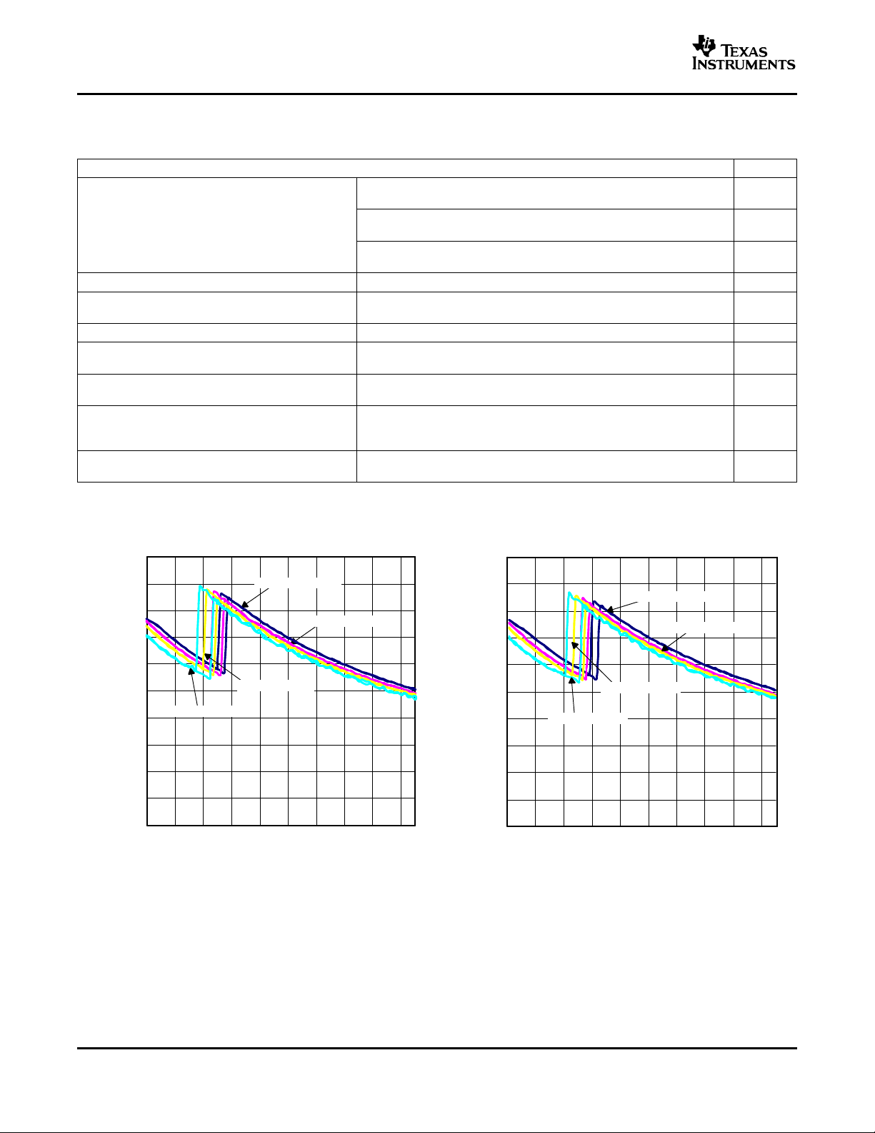
Figure 7. Figure 8.
DIMMING RESPONSE DIMMING RESPONSE
8
Figure 9. Figure 10.
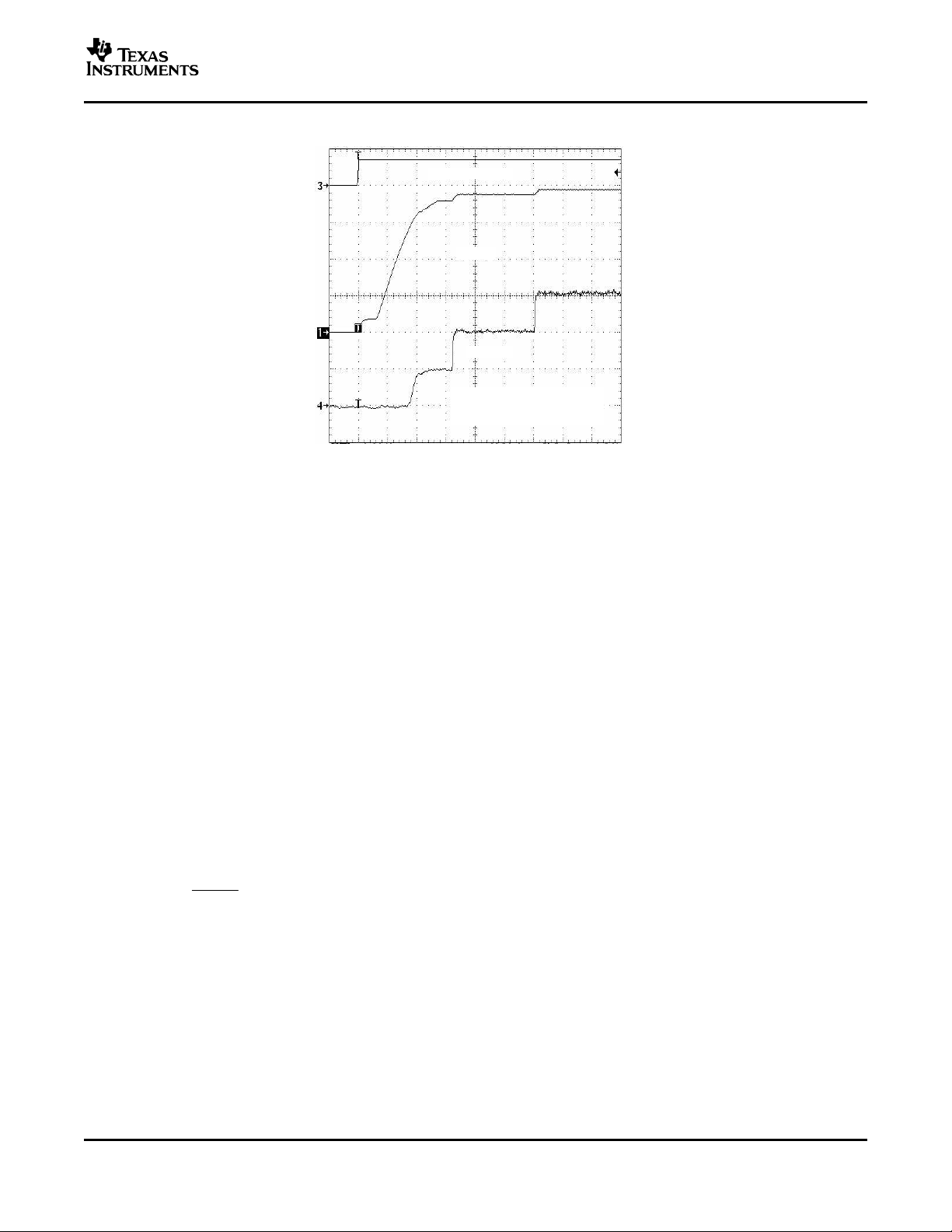
www.ti.com
EN1 + EN2
V
O
I
LED
0 V
0 A
0 V
20 mA/div 5 V/div1 V/div
20 s/div
VI = 3.6 V , I
LED
= 20 mA,
3 LED’s Connected,
TA = 25C
R
ISET
V
ISET
I
LED
K
STARTUP TIMING
TPS60231
SLVS544 – OCTOBER 2004
Figure 11.
DETAILED DESCRIPTION
OPERATION
The TPS60231 uses a fractional conversion charge pump to generate a supply voltage for the integrated current
sinks. These current sinks are used to ensure a constant current for each LED. Depending on the input voltage
and programmed LED current, the charge pump either operates in the 1x mode or in the 1.5x mode. By
switching automatically between these two modes, the circuit optimizes power conversion efficiency as well as
extends operating time by allowing the discharge of the battery completely.
The charge pump can generate 75 mA of output current, so each of the 3 LED outputs can be powered with up
to 25 mA of current. The maximum LED current is set by a resistor connected to the ISET pin. This resistor
programs a reference current, which is current mirrored to set the LED current.
Applying a PWM signal to the EN1 pin and/or the EN2 pin controls the LED brightness. See a detailed
description in the section Analog Dimming Using ISET Pin.
LED CURRENT ADJUSTMENT (ISET)
A resistor programs a reference current, which is current mirrored to set the LED current. The voltage at the
ISET pin depends on the status of EN1 and EN2. The current in each LED is typically 260 times the current
through the resistor at ISET.
V
— Voltage from ISET pin (0.2 V, 0.4 V or 0.6 V) to GND, see Table 1
ISET
I
— Current per LED from Dx pin to GND
LED
K — Dx to I
The LED current varies linearly from 0 mA to I
The LED brightness can however also be controlled by an analog control signal that is fed into the ISET pin.
current ratio (typically 260)
SET
LED(max)
mA by applying a PMW signal with 0% to 100% duty cycle.
9

www.ti.com
TPS60231
SLVS544 – OCTOBER 2004
DETAILED DESCRIPTION (continued)
SOFT START
The TPS60231 has an internal soft start circuit to limit the inrush current during startup. This prevents possible
voltage drops of the input voltage if a high impedance power source is connected to the input of the TPS60231.
When the device starts up with an output voltage that is below the input voltage, the output capacitor is charged
directly from the input with a current source. The output current increases linearly until the output reaches within
300 mV of the input voltage. When the programmed output current can be reached with the 1x mode, the
TPS60231 terminates the soft start and begins normal operation. When the desired output current cannot be
reached, the charge pump begins operation in 1.5x mode and pumps the output voltage up to the needed level
to reach the programmed output current.
ENABLE (EN1, EN2)
The enable pins EN1 and EN2 are used to enable the device or set it into shutdown. The TPS60231 is enabled if
one of the enable pins is pulled higher than the enable trip point of 1.3 V. The device starts up by going through
the soft start routine as described in the section Soft Start. Pulling both pins to GND, after a delay, programs the
device to shutdown. In shutdown, the charge pump, current sources, voltage reference, oscillator, and all other
functions are turned off and the supply current is reduced to 0.1 µA.
EN1 and EN2 can also be used for dimming. The logic levels at EN1 and EN2 set the minimum voltage at the
current mirrors and the voltage at the ISET pin to GND. This sets the current at the LEDs to be either the full
current or a fraction of the full current. See Table 1 for further details. The maximum current through the LEDs is
set by a resistor connected between ISET and GND.
EN1 and EN2 can also be used for PWM dimming. The PWM signal can either be applied to EN1 or EN2, or
both inputs can be tied together and the PWM signal can be applied to both pins. Depending on the
configuration, the current during PWM dimming is switched between 0 mA and its maximum (EN1 and EN2
connected to the PWM signal) or between 0 mA and 1/3 of the full LED current if EN2 = 0 and EN1 is toggled.
When EN1 = 0 and EN2 is toggled, the output current can be changed between 0 mA and 2/3 of the full range.
Table 1. Enable Levels
ENABLE LEVEL
EN2 EN1
0 0 SHUTDOWN 0
0 1 VISET = 200 mV 1/3
1 0 VISET = 400 mV 2/3
1 1 VISET = 600 mV Full
MODE LED CURRENT
UNDERVOLTAGE LOCKOUT
The undervoltage lockout circuit shuts down the device when the voltage at VIN drops below a typical threshold
of 2.15 V. This prevents damage to the device. The UVLO circuit allows the device to start up again after the
voltage on the VIN pin has increased by about 50 mV above the UVLO lockout threshold.
SHORT CIRCUIT AND OVERTEMPERTURE PROTECTION
The current at the VOUT pin is limited typically to 250 mA. When the junction temperature exceeds 160 ° C, the
device shuts down to protect the device from damage. After the temperature decreases to about 140 ° C, the
device starts up again if it is enabled.
OVERVOLTAGE PROTECTION AT VOUT
The device uses the voltage at D1 to regulate voltage at VOUT. In case D1 is not connected, an overvoltage
protection circuit ensures that the output voltage at VOUT does not exceed its limits. The connection of the LEDs
must be started using D1 first. For all other LEDs there is no restriction in the sequence. For example, if there
are only 2 LEDs used, the first LED is connected to D1 and the other LED can be connected to any other of the
D2 to D3 pins.
10

www.ti.com
P
D max, package
T
Jmax
T
A
R
ja
TPS60231
SLVS544 – OCTOBER 2004
THEORY OF OPERATION/DESIGN PROCEDURE
Capacitor Selection
Ceramic capacitors such as X5R or X7R are recommended to be used with the TPS60231. For the two flying
capacitors C1 and C2, it is important to use low ESR capacitors to avoid unnecessary efficiency losses. Low
ESR capacitors on VOUT reduce the ripple voltage on the supply of the current sources. Table 2 lists capacitor
types that have been tested with the TPS60231.
Table 2. Capacitors
PART VALUE VOLTAGE MANUFACTURER SIZE WEBSITE
C1608X5R1A105M 1 µ F 10 V 0603
C1608X5R1A474M 0.47 µ F 10 V TDK 0603 www.componnent.tdk.com
C2012X7R1C105M 1 µ F 16 V 0805
LMK107BJ105MA 1 µ F 10 V 0603
LMK107BJ474MA 0.47 µ F 10 V Taiyo Yuden 0603 www.t-yuden.com
LMK212BJ105MG 1 µ F 10 V 0805
Power Efficiency
The power conversion efficiency of the TPS60231 can be calculated by adding up the products of each LED
current and voltage and dividing it by the product of the input voltage and current. With a fully charged battery
where the input voltage is typically above the LED forward voltage, the charge pump operates in the 1x mode
and efficiency is very high. As the battery discharges, there is a point where the current sources no longer have
enough voltage overhead to maintain a constant current regulation. At that point, the charge pump switches into
the 1.5x mode. The conversion efficiency is lowest at the crossover. As the battery discharges further, the
efficiency again increases until at about 3.1 V where it reaches a second maximum. Below 3.1 V input voltage,
the maximum current per LED is less than 25 mA.
Power Dissipation
The maximum power dissipation inside the TPS60231 can be calculated based on the following equation:
P
= [(1.5 × VI) – V
D max
+ 0.4 V] × I
O
O
The maximum power dissipation occurs when the input voltage is just low enough to operate in 1.5x mode, with
a forward voltage of the white LED at maximum. This is typically for VI= 4.2 V and a forward voltage of 3.6 V.
This needs to be lower than the maximum allowed power dissipation of the package, which can be calculated
using the following equation:
For example, the worst case power dissipation occurs at the input voltage level where the charge pump switches
from the 1x mode to the 1.5x mode. At this operating point, the supply voltage to the current sources is at its
maximum and the current sources must drop the most voltage in order to maintain a regulated output current.
The worst case power dissipation occurs when all 3 LED outputs are fully loaded with 25 mA of LED current.
• With: VI= 4.2 V, Vf= 3.6 V, IO= 75 mA (1.5x mode)
• P
= 0.23 W
D max
11

www.ti.com
VIN
C1+
C1−
C2+
C2−
EN1
EN2
GND
VOUT
D1
D2
D3
ISET
0.47 F
0.47 F
1 F
1 F
VIN = 2.7 V
to 6.5 V
Typical Smartphone Display
PGND
VIN
C1+
C1−
C2+
C2−
EN1
EN2
GND
VOUT
D1
D2
D3
ISET
0.47 F
0.47 F
1 F
1 F
VIN = 2.7 V
to 6.5 V
6 k
V = 0 mV to
600 mV
PGND
TPS60231
SLVS544 – OCTOBER 2004
APPLICATION INFORMATION
TYPICAL APPLICATION OF A SMART PHONE DISPLAY WITH RESISTORS CONNECTED IN PARALLEL
If more than 25 mA of output current is needed, then the input pins to the current sinks can be connected in
parallel as shown in the following application figure. This method can also be used to connect a LC display with
only two connections for the white LEDs.
Figure 12. Typical Application With Resistors in Parallel
ANALOG DIMMING USING ISET PIN
The ISET pin can be used to connect an analog dc signal in the range of 0 mV to 600 mV (EN1 = EN2 = 1) for
analog dimming of the white LEDs. For an input voltage of 0 V at ISET, the current is at its maximum, whereas at
600 mV, the LED current is zero. The maximum current is:
• For EN2 = EN1 = 1: ILED = Vset/Rset × K = 0.6V/6kR × 260 = 26 mA per LED
• For EN2 = 1, EN0 = 1: ILED = Vset/Rset × K = 0.4V/6kR × 260 = 17 mA per LED
• For EN2 = 0, EN1 = 1: ILED = Vset/Rset × K = 0.2V/6kR × 260 = 8.6 mA per LED
• With EN2, EN1 set to 10 or 01, a voltage of 400 mV or 200 mV is required to set the LED current to zero.
12
Figure 13. Analog Dimming Connections Using ISET Pin

www.ti.com
V
OUT
= VD1 + V
FLEDD1
R
g
V
FLEDD1
V
Fg
I
g
VIN
C1+
C1−
C2+
C2−
EN1
EN2
GND
VOUT
D1
D2
D3
ISET
0.47 F
0.47 F
1 F
1 F
VIN = 2.7 V
to 6.5 V
6 Green
LEDs With
4 mA Each
2 White
LEDs With
25 mA Each
6.2 k
Sets Current to 25 mA
Per Current Sink
(With EN2 = EN1 = 1)
Rg = 220
TPS60231
SLVS544 – OCTOBER 2004
APPLICATION INFORMATION (continued)
TYPICAL APPLICATION USING 2 WHITE LEDs AND 6 GREEN LEDs FOR LCD BACKLIGHT AND
KEYBOARD LIGHTING
The TPS60231 can be used to power any kind of LED. It is also possible to mix white LEDs with color LEDs
which have a lower forward voltage. The LED with the highest forward voltage (typically the white LED) has to be
connected to D1, because the output voltage of the charge pump is regulated in such a way to keep the voltage
drop from D1 to GND at 400mV (with EN1 = EN2 = 1). Therefore the output voltage of the charge pump is
regulated to:
V
— Output voltage at VOUT
OUT
V
— Voltage from D1 to GND (Vsource at D1 pin, see electrical characteristics)
D1
V
Resistor R
V
Ig— Current per green LED
— Forward voltage of the LED connected to D1
FLEDD1
is used to provide current sharing between the 6 green LEDs. The upper value is calculated using:
g
— Forward voltage of a green LED
Fg
Figure 14. LED Connections for LCD Backlight and Keyboard Lighting
PROPOSED LAND PATTERN FOR PCB PRODUCTION
Refer to the application note SLUA271 for the proposed land pattern of the QFN package.
13

PACKAGE OPTION ADDENDUM
www.ti.com
27-Feb-2006
PACKAGING INFORMATION
Orderable Device Status
(1)
Package
Type
Package
Drawing
Pins Package
Qty
Eco Plan
TPS60231RGTR ACTIVE QFN RGT 16 3000 Green (RoHS &
no Sb/Br)
TPS60231RGTRG4 ACTIVE QFN RGT 16 3000 Green (RoHS &
no Sb/Br)
TPS60231RGTT ACTIVE QFN RGT 16 250 Green (RoHS &
no Sb/Br)
TPS60231RGTTG4 ACTIVE QFN RGT 16 250 Green (RoHS &
no Sb/Br)
(1)
The marketing status values are defined as follows:
ACTIVE: Product device recommended for new designs.
LIFEBUY: TI has announced that the device will be discontinued, and a lifetime-buy period is in effect.
NRND: Not recommended for new designs. Device is in production to support existing customers, but TI does not recommend using this part in
a new design.
PREVIEW: Device has been announced but is not in production. Samples may or may not be available.
OBSOLETE: TI has discontinued the production of the device.
(2)
Eco Plan - The planned eco-friendly classification: Pb-Free (RoHS), Pb-Free (RoHS Exempt), or Green (RoHS & no Sb/Br) - please check
http://www.ti.com/productcontent for the latest availability information and additional product content details.
TBD: The Pb-Free/Green conversion plan has not been defined.
Pb-Free (RoHS): TI's terms "Lead-Free" or "Pb-Free" mean semiconductor products that are compatible with the current RoHS requirements
for all 6 substances, including the requirement that lead not exceed 0.1% by weight in homogeneous materials. Where designed to be soldered
at high temperatures, TI Pb-Free products are suitable for use in specified lead-free processes.
Pb-Free (RoHS Exempt): This component has a RoHS exemption for either 1) lead-based flip-chip solder bumps used between the die and
package, or 2) lead-based die adhesive used between the die and leadframe. The component is otherwise considered Pb-Free (RoHS
compatible) as defined above.
Green (RoHS & no Sb/Br): TI defines "Green" to mean Pb-Free (RoHS compatible), and free of Bromine (Br) and Antimony (Sb) based flame
retardants (Br or Sb do not exceed 0.1% by weight in homogeneous material)
(2)
Lead/Ball Finish MSL Peak Temp
CU NIPDAU Level-2-260C-1 YEAR
CU NIPDAU Level-2-260C-1 YEAR
CU NIPDAU Level-2-260C-1 YEAR
CU NIPDAU Level-2-260C-1 YEAR
(3)
(3)
MSL, Peak Temp. -- The Moisture Sensitivity Level rating according to the JEDEC industry standard classifications, and peak solder
temperature.
Important Information and Disclaimer:The information provided on this page represents TI's knowledge and belief as of the date that it is
provided. TI bases its knowledge and belief on information provided by third parties, and makes no representation or warranty as to the
accuracy of such information. Efforts are underway to better integrate information from third parties. TI has taken and continues to take
reasonable steps to provide representative and accurate information but may not have conducted destructive testing or chemical analysis on
incoming materials and chemicals. TI and TI suppliers consider certain information to be proprietary, and thus CAS numbers and other limited
information may not be available for release.
In no event shall TI's liability arising out of such information exceed the total purchase price of the TI part(s) at issue in this document sold by TI
to Customer on an annual basis.
Addendum-Page 1


IMPORTANT NOTICE
Texas Instruments Incorporated and its subsidiaries (TI) reserve the right to make corrections, modifications,
enhancements, improvements, and other changes to its products and services at any time and to discontinue
any product or service without notice. Customers should obtain the latest relevant information before placing
orders and should verify that such information is current and complete. All products are sold subject to TI’s terms
and conditions of sale supplied at the time of order acknowledgment.
TI warrants performance of its hardware products to the specifications applicable at the time of sale in
accordance with TI’s standard warranty. Testing and other quality control techniques are used to the extent TI
deems necessary to support this warranty . Except where mandated by government requirements, testing of all
parameters of each product is not necessarily performed.
TI assumes no liability for applications assistance or customer product design. Customers are responsible for
their products and applications using TI components. To minimize the risks associated with customer products
and applications, customers should provide adequate design and operating safeguards.
TI does not warrant or represent that any license, either express or implied, is granted under any TI patent right,
copyright, mask work right, or other TI intellectual property right relating to any combination, machine, or process
in which TI products or services are used. Information published by TI regarding third-party products or services
does not constitute a license from TI to use such products or services or a warranty or endorsement thereof.
Use of such information may require a license from a third party under the patents or other intellectual property
of the third party, or a license from TI under the patents or other intellectual property of TI.
Reproduction of information in TI data books or data sheets is permissible only if reproduction is without
alteration and is accompanied by all associated warranties, conditions, limitations, and notices. Reproduction
of this information with alteration is an unfair and deceptive business practice. TI is not responsible or liable for
such altered documentation.
Resale of TI products or services with statements different from or beyond the parameters stated by TI for that
product or service voids all express and any implied warranties for the associated TI product or service and
is an unfair and deceptive business practice. TI is not responsible or liable for any such statements.
Following are URLs where you can obtain information on other Texas Instruments products and application
solutions:
Products Applications
Amplifiers amplifier.ti.com Audio www.ti.com/audio
Data Converters dataconverter.ti.com Automotive www.ti.com/automotive
DSP dsp.ti.com Broadband www.ti.com/broadband
Interface interface.ti.com Digital Control www.ti.com/digitalcontrol
Logic logic.ti.com Military www.ti.com/military
Power Mgmt power.ti.com Optical Networking www.ti.com/opticalnetwork
Microcontrollers microcontroller.ti.com Security www.ti.com/security
Low Power Wireless www.ti.com/lpw Telephony www.ti.com/telephony
Video & Imaging www.ti.com/video
Wireless www.ti.com/wireless
Mailing Address: Texas Instruments
Post Office Box 655303 Dallas, Texas 75265
Copyright 2006, Texas Instruments Incorporated
 Loading...