

Texas Instruments TPS3836K33DBVT, TPS3836K33DBVR, TPS3836J25DBVT, TPS3836J25DBVR, TPS3836H30DBVT Datasheet
...
TPS3836E18 / J25 / H30 / L30 / K33
TPS3837E18 / J25 / L30 / K33, TPS3838E18 / J25 / L30 / K33
NANOPOWER SUPERVISORY CIRCUITS
SLVS292A – JUNE 2000 – REVISED JANUARY 2002
D Supply Current of 220 nA (Typ)
D Precision Supply Voltage Supervision
Range: 1.8 V, 2.5 V, 3.0 V, 3.3 V
D Power-On Reset Generator With Selectable
Delay Time of 10 ms or 200 ms
D Push/Pull RESET Output (TPS3836),
RESET Output (TPS3837), or
Open-Drain RESET
Output (TPS3838)
D Manual Reset
D 5-Pin SOT-23 Package
D Temperature Range –40°C to 85°C
D Applications Include
– Applications Using Low-Power DSPs,
Microcontrollers, or Microprocessors
– Portable/Battery-Powered Equipment
– Intelligent Instruments
– Wireless Communication Systems
– Notebook Computers
– Automotive Systems
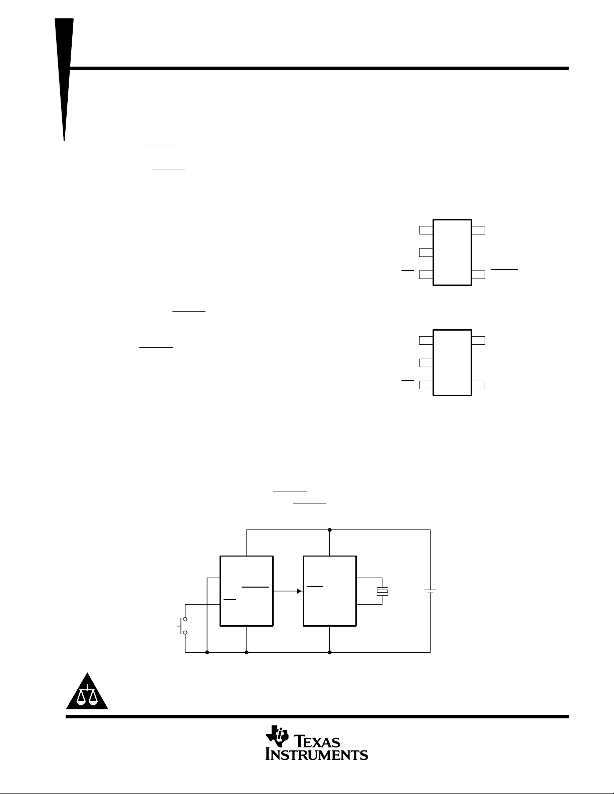
TPS3836, TPS3838
DBV PACKAGE
(TOP VIEW)
CT
1
description
GND
The TPS3836, TPS3837, TPS3838 families of
supervisory circuits provide circuit initialization
MR
and timing supervision, primarily for DSP and
processor-based systems.
During power on, RESET
supply voltage V
DD
Thereafter, the supervisory circuit monitors V
and keeps RESET output active as long as V
remains below the threshold voltage VIT. An
is asserted when the
becomes higher than 1.1 V.
DD
DD
CT
GND
internal timer delays the return of the output to the
inactive state (high) to ensure proper system
reset. The delay time starts after V
above the threshold voltage V
.
IT
has risen
DD
MR
When CT is connected to GND a fixed delay time of typical 10 ms is asserted. When connected to V
time is typically 200 ms.
2
3
TPS3837
DBV PACKAGE
(TOP VIEW)
1
2
3
5
V
DD
4
RESET
V
5
4
DD
RESET
the delay
DD
When the supply voltage drops below the threshold voltage V
All the devices of this family have a fixed-sense threshold voltage V
The TPS3836 has an active-low push-pull RESET
TPS3838 integrates an active-low open-drain RESET
TPS3836K33
V
DD
CT
RESET
MR
T
Please be aware that an important notice concerning availability, standard warranty, and use in critical applications of
Texas Instruments semiconductor products and disclaimers thereto appears at the end of this data sheet.
PRODUCTION DATA information is current as of publication date.
Products conform to specifications per the terms of Texas Instruments
standard warranty. Production processing does not necessarily include
testing of all parameters.
GND
TYPICAL OPERATING CIRCUIT
output. The TPS3837 has active-high push-pull RESET , and
output.
V
CC
RST
Xout
V
SS
MSP430
Xin
, the output becomes active (low) again.
IT
set by an internal voltage divider.
IT
Lithium
Battery
Quartz
32 kHz
3.6 V
Copyright 2002, Texas Instruments Incorporated
POST OFFICE BOX 655303 • DALLAS, TEXAS 75265
1
TPS3836E18 / J25 / H30 / L30 / K33
40 C to 85 C
TPS3837E18 / J25 / L30 / K33, TPS3838E18 / J25 / L30 / K33
NANOPOWER SUPERVISORY CIRCUITS
SLVS292A – JUNE 2000 – REVISED JANUARY 2002
description (continued)
The product spectrum is designed for supply voltages of 1.8 V , 2.5 V, 3 V , and 3.3 V. The circuits are available
in a 5-pin SOT-23 package. The TPS3836, TPS3837, TPS3838 families are characterized for operation over
a temperature range of –40°C to 85°C.
PACKAGE INFORMATION
T
A
TPS3836E18DBVR
TPS3836J25DBVR
TPS3836H30DBVR
TPS3836L30DBVR
TPS3836K33DBVR
TPS3837E18DBVR
–40°C to 85°C
†
The DBVR passive indicates tape and reel of 3000 parts.
‡
The DBVT passive indicates tape and reel of 250 parts.
TPS3837J25DBVR
TPS3837L30DBVR
TPS3837K33DBVR
TPS3838E18DBVR
TPS3838J25DBVR
TPS3838L30DBVR
TPS3838K33DBVR
DEVICE NAME THRESHOLD VOLTAGE SYMBOL
†
TPS3836E18DBVT
†
TPS3836J25DBVT
†
TPS3836H30DBVT
†
TPS3836L30DBVT
†
TPS3836K33DBVT
†
TPS3837E18DBVT
†
TPS3837J25DBVT
†
TPS3837L30DBVT
†
TPS3837K33DBVT
†
TPS3838E18DBVT
†
TPS3838J25DBVT
†
TPS3838L30DBVT
†
TPS3838K33DBVT
‡
‡
‡
‡
‡
‡
‡
‡
‡
‡
‡
‡
‡
1.71 V PDNI
2.25 V PDSI
2.79 V PHRI
2.64 V PCAI
2.93 V PDTI
1.71 V PDOI
2.25 V PDRI
2.64 V PCBI
2.93 V PDUI
1.71 V PDQI
2.25 V PDPI
2.64 V PCCI
2.93 V PDVI
ORDERING INFORMATION
TPS383 6 E 18 DBV R
FUNCTION TABLE TPS3836, TPS3837, TPS3838
MR
L 0 L H
L 1LH
H 0LH
H 1 H L
§
TPS3836 and TPS3838
¶
TPS3837
VDD > V
IT
Reel
Package
Nominal Supply Voltage
Typical Reset Threshold Voltage
Functionality
Family
RESET
§
RESET
¶
2
POST OFFICE BOX 655303 • DALLAS, TEXAS 75265
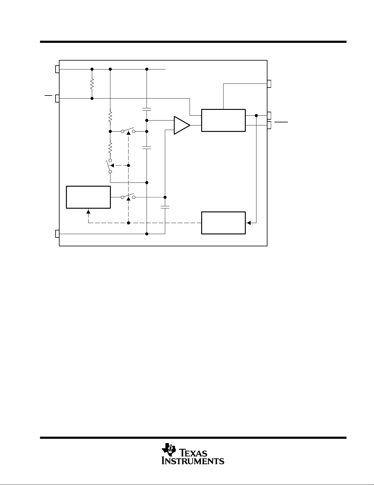
functional block diagram
V
DD
TPS3836E18 / J25 / H30 / L30 / K33
TPS3837E18 / J25 / L30 / K33, TPS3838E18 / J25 / L30 / K33
NANOPOWER SUPERVISORY CIRCUITS
SLVS292A – JUNE 2000 – REVISED JANUARY 2002
MR
GND
R3
Band-Gap
Reference
R1
R2
S2
S1
S3
C1
C2
C3
C
T
+
–
Reset Logic
and Timer
Refresh
Timer
Reset (TPS3837-Push-Pull)
Reset (TPS3836-Push-Pull
TPS3838-Open-Drain)
POST OFFICE BOX 655303 • DALLAS, TEXAS 75265
3
TPS3836E18 / J25 / H30 / L30 / K33
TPS3837E18 / J25 / L30 / K33, TPS3838E18 / J25 / L30 / K33
NANOPOWER SUPERVISORY CIRCUITS
SLVS292A – JUNE 2000 – REVISED JANUARY 2002
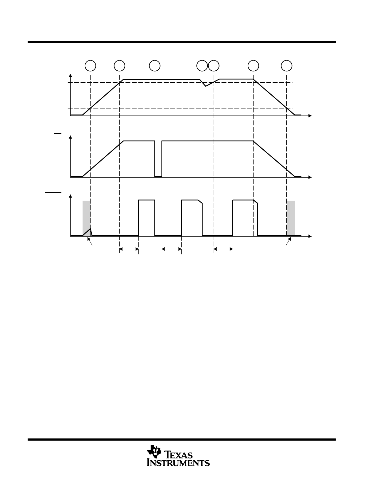
timing diagram
V
DD
< 1.1 V
MR
RESET
A
V
IT
B C D E F G
t
t
t
Undefined
Output
t
d
t
d
t
d
Undefined
Output
4
POST OFFICE BOX 655303 • DALLAS, TEXAS 75265

TPS3836E18 / J25 / H30 / L30 / K33
TPS3837E18 / J25 / L30 / K33, TPS3838E18 / J25 / L30 / K33
NANOPOWER SUPERVISORY CIRCUITS
SLVS292A – JUNE 2000 – REVISED JANUARY 2002
absolute maximum ratings over operating free-air temperature range (unless otherwise noted)
Supply voltage, V
(see Note 1) 7 V. . . . . . . . . . . . . . . . . . . . . . . . . . . . . . . . . . . . . . . . . . . . . . . . . . . . . . . . . . . . .
DD
†
All other pins (see Note 1) –0.3 V to 7 V. . . . . . . . . . . . . . . . . . . . . . . . . . . . . . . . . . . . . . . . . . . . . . . . . . . . . . . . . . .
Maximum low output current, I
Maximum high output current, I
Input clamp current, I
Output clamp current, I
IK
(V
OK
< 0 or V
I
(V
O
OL
OH
> VDD) ±10 mA. . . . . . . . . . . . . . . . . . . . . . . . . . . . . . . . . . . . . . . . . . . . . . . . .
I
< 0 or V
> VDD) ±10 mA. . . . . . . . . . . . . . . . . . . . . . . . . . . . . . . . . . . . . . . . . . . .
O
5 mA. . . . . . . . . . . . . . . . . . . . . . . . . . . . . . . . . . . . . . . . . . . . . . . . . . . . . . . . . . . .
–5 mA. . . . . . . . . . . . . . . . . . . . . . . . . . . . . . . . . . . . . . . . . . . . . . . . . . . . . . . . . .
Continuous total power dissipation See Dissipation Rating Table. . . . . . . . . . . . . . . . . . . . . . . . . . . . . . . . . . . . . .
Operating free-air temperature range, T
Storage temperature range, T
stg
A
–40°C to 85°C. . . . . . . . . . . . . . . . . . . . . . . . . . . . . . . . . . . . . . . . . . . . .
–65°C to 150°C. . . . . . . . . . . . . . . . . . . . . . . . . . . . . . . . . . . . . . . . . . . . . . . . . . . .
Soldering temperature 260°C. . . . . . . . . . . . . . . . . . . . . . . . . . . . . . . . . . . . . . . . . . . . . . . . . . . . . . . . . . . . . . . . . . . .
†
Stresses beyond those listed under “absolute maximum ratings” may cause permanent damage to the device. These are stress ratings only, and
functional operation of the device at these or any other conditions beyond those indicated under “recommended operating conditions” is not
implied. Exposure to absolute-maximum-rated conditions for extended periods may affect device reliability.
NOTE 1: All voltage values are with respect to GND. For reliable operation, the device must not be operated at 7 V for more than t=1000 h
continuously
DISSIPATION RATING TABLE
PACKAGE
DBV 437 mW 3.5 mW/ºC 280 mW 227 mW
TA <25°C
POWER RATING
DERATING FACTOR
ABOVE TA = 25°C
TA = 70°C
POWER RATING
POWER RATING
TA = 85°C
recommended operating conditions at specified temperature range
MIN MAX UNIT
Supply voltage, V
Input voltage, V
High-level input voltage, V
Low-level input voltage, V
Input transition rise and fall rate at MR, ∆t/∆V 100 ns/V
Operating free-air temperature range, T
DD
I
IH
IL
A
1.6 6 V
0 VDD + 0.3 V
0.7 × V
DD
0.3 × V
–40 85 °C
DD
V
V
POST OFFICE BOX 655303 • DALLAS, TEXAS 75265
5

TPS3836E18 / J25 / H30 / L30 / K33
RESET
0.8 ×
RESET
DD
RESET
RESET
V
IT
3)
T
A
40 C to 85 C
V
y
V
hys
Hysteresis at V
DD
in ut
mV
IIHHigh level in ut current
IILLow level in ut current
IDDSu ly current
TPS3837E18 / J25 / L30 / K33, TPS3838E18 / J25 / L30 / K33
NANOPOWER SUPERVISORY CIRCUITS
SLVS292A – JUNE 2000 – REVISED JANUARY 2002
electrical characteristics over recommended operating conditions (unless otherwise noted)
PARAMETER TEST CONDITION MIN
RESET
V
OH
V
OL
V
IT
V
h
I
I
I
OH
I
DD
C
I
NOTES: 2. The lowest voltage at which RESET output becomes active. tr, VDD ≥ 15 µs/V
High-level output voltage
Low-level output voltage
Power-up reset voltage
(see Note 2)
Negative-going input threshold
voltage (see Note
Hysteresis at VDD input
s
High-level input current
Low-level input current
High-level output current TPS3838 VDD = VIT + 0.2 V, VOH = V
Supply current
Internal pullup resistor at MR 30 kΩ
Input capacitance at MR, CT VI = 0 V to V
3. To ensure best stability of the threshold voltage, a bypass capacitor (ceramic, 0.1 µF) should be placed near the supply terminal.
4. If manual reset is unused, MR
(TPS3836)
RESET
(TPS3837)
RESET
(TPS3836/8)
RESET
(TPS3837)
TPS3836/8 VDD ≥ 1.1 V, IOL = 50 µA 0.2
TPS3837
TPS383xE18 1.66 1.71 1.74
TPS383xJ25 2.18 2.25 2.29
TPS383xH30
TPS383xL30
TPS383xK33 2.84 2.93 2.99
MR
(see Note 4)
CT CT = VDD = 6 V –25 25 nA
MR
(see Note 4)
CT CT = 0 V, VDD = 6 V –25 25 nA
should be connected to VDD to minimize current consumption.
VDD = 3.3 V, IOH = –2 mA
VDD = 6 V, IOH = –3 mA
VDD = 1.8 V, IOH = –1 mA
VDD = 3.3 V, IOL = –2 mA
VDD = 1.8 V, IOL = 1 mA
VDD = 3.3 V, IOL = 2 mA
VDD = 3.3 V, IOL = 2 mA
VDD = 6 V, IOL = 3 mA
VDD ≥ 1.1 V, IOH = –50 µA
TA = –40°C to 85°C
1.7 V < VIT < 2.5 V 30
2.5 V < VIT < 3.5 V
3.5 V < VIT < 5 V 50
MR = 0.7 × VDD, VDD = 6 V –40 –60 –100
MR = 0 V, VDD = 6 V –130 –200 –340
VDD > VIT, VDD < 3 V 220 400
VDD > VIT, VDD > 3 V
VDD < V
IT
DD
DD
TYP
MAX UNIT
0.8 ×
V
DD
0.8 ×
V
DD
2.70 2.79 2.85
2.56 2.64 2.69
40
250 450
10 15
5 pF
0.4 V
25 nA
V
V
V
mV
µA
µA
nA
µA
6
POST OFFICE BOX 655303 • DALLAS, TEXAS 75265

TPS3836E18 / J25 / H30 / L30 / K33
µ
t
PHL
Pro agation (delay) time, high to low level out ut
µs
µ
t
PLH
Pro agation (delay) time, low to high level out ut
µs
V
IL
V
DD
TPS3837E18 / J25 / L30 / K33, TPS3838E18 / J25 / L30 / K33
NANOPOWER SUPERVISORY CIRCUITS
SLVS292A – JUNE 2000 – REVISED JANUARY 2002
timing requirements at R
PARAMETER TEST CONDITIONS MIN TYP MAX UNIT
t
w
Pulse width
= 1 MΩ, C
L
switching characteristics at R
PARAMETER TEST CONDITIONS MIN TYP MAX UNIT
t
Delay time
d
t
Propagation (delay) time, high-to-low-level output
t
Propagation (delay) time, low-to-high-level output
t
Propagation (delay) time, high-to-low-level output
PHL
t
Propagation (delay) time, low-to-high-level output
PLH
L
at V
DDVIH
at MR
= 1 MΩ, C
L
= 50 pF, T
= VIT + 0.2 V, VIL = VIT – 0.2 V 6
VDD ≥ VIT + 0.2 V, VIL = 0.3 × V
VIH = 0.7 × V
= 50 pF, T
L
VDD to RESET delay
(TPS3836, TPS3838)
VDD to RESET delay
(TPS3837)
MR to RESET delay
(TPS3836, TPS3838)
MR to RESET delay
(TPS3837)
= 25_C
A
DD
DD,
= 25_C
A
VDD ≥ VIT + 0.2 V,
MR
= 0.7 × VDD,
CT = GND,
See timing diagram
VDD≥ VIT + 0.2 V,
= 0.7 × VDD,
MR
CT = VDD ,
See timing diagram
VIL = VIT – 0.2 V,
VIH = VIT + 0.2 V
VIL = 1.6 V 50
VIL = VIT – 0.2 V,
VIH = VIT + 0.2 V
VIL = 1.6 V 50
VDD ≥ VIT + 0.2 V,
= 0.3 × V
= 0.3 ×
V
VIL = 0.7 × V
DD
,
,
1
5 10 15
100 200 300
10
10
0.1
0.1 µs
µs
µs
ms
s
s
µs
I
I
V
V
DD
MR
OL
OH
TYPICAL CHARACTERISTICS
Table of Graphs
FIGURE
Supply current vs Supply voltage 1
Manual reset current vs Manual reset voltage 2
Low-level output voltage vs Low-level output current 3
High-level output voltage vs High-level output current 4
Normalized reset threshold voltage vs Free-air temperature 5
Minimum pulse duration at V
DD
vs VDD Threshold overdrive 6
POST OFFICE BOX 655303 • DALLAS, TEXAS 75265
7

TPS3836E18 / J25 / H30 / L30 / K33
TPS3837E18 / J25 / L30 / K33, TPS3838E18 / J25 / L30 / K33
NANOPOWER SUPERVISORY CIRCUITS
SLVS292A – JUNE 2000 – REVISED JANUARY 2002
TYPICAL CHARACTERISTICS
SUPPLY CURRENT
vs
SUPPLY VOLTAGE
10
MR = Open
CT = GND
8
6
4
– Supply Current – µA
DD
I
2
0
0246
VDD – Supply Voltage – V
TA = 85°C
TA = 25°C
TA = 0°C
TA = –40°C
Figure 1
MANUAL RESET CURRENT
vs
MANUAL RESET VOLTAGE
100
VDD = 6 V
CT = GND
0
TA = –40°C
– Manual Reset Current – µA
MR
I
–100
–200
–300
–400
–500
TA = 0°C
TA = 25°C
TA = 85°C
–20246
VMR – Manual Reset Voltage – V
Figure 2
LOW-LEVEL OUTPUT VOLTAGE
vs
LOW-LEVEL OUTPUT CURRENT
2.0
VDD = 2 V
MR = OPEN
CT = GND
1.5
TA = 25°C
1.0
TA = 85°C
0.5
– Low-Level Output Voltage – V
OL
V
0.0
01234567
IOL – Low-Level Output Current – mA
TA = –40°C
Figure 3
TA = 0°C
HIGH-LEVEL OUTPUT VOLTAGE
vs
HIGH-LEVEL OUTPUT CURRENT
2.0
1.5
TA = 85°C
TA = 25°C
1.0
TA = 0°C
0.5
– High-Level Output Voltage – V
OH
V
0.0
012345
IOH – High-Level Output Current – mA
TA = –40°C
VDD = 2 V
MR
= OPEN
CT = GND
Figure 4
8
POST OFFICE BOX 655303 • DALLAS, TEXAS 75265

1.001
0.999
0.998
TPS3836E18 / J25 / H30 / L30 / K33
TPS3837E18 / J25 / L30 / K33, TPS3838E18 / J25 / L30 / K33
NANOPOWER SUPERVISORY CIRCUITS
SLVS292A – JUNE 2000 – REVISED JANUARY 2002
TYPICAL CHARACTERISTICS
NORMALIZED RESET THRESHOLD
VOLTAGE
vs
FREE-AIR TEMPERATURE
1
0.997
0.996
Normalized Reset Threshold Voltage – V
0.995
–40 –15 10 35 60 85
TA – Free-Air Temperature – °C
CT = GND,
MR
= Open
Figure 5
MINIMUM PULSE DURATION AT V
vs
THRESHOLD OVERDRIVE
V
DD
MR = Open
CT = GND
TA = 25°C
– µs
DD
22
20
18
16
14
12
10
8
DD
6
4
Minimum Pulse Duration at V
2
0
0 0.2 0.4 0.6 0.8 1 1.2 1.4 1.6 1.8 2
VDD – Threshold Overdrive – V
Figure 6
POST OFFICE BOX 655303 • DALLAS, TEXAS 75265
9

TPS3836E18 / J25 / H30 / L30 / K33
TPS3837E18 / J25 / L30 / K33, TPS3838E18 / J25 / L30 / K33
NANOPOWER SUPERVISORY CIRCUITS
SLVS292A – JUNE 2000 – REVISED JANUARY 2002
MECHANICAL DATA
DBV (R-PDSO-G5) PLASTIC SMALL-OUTLINE
0,95
1,45
0,95
3,00
2,80
45
31
0,05 MIN
0,50
0,30
1,70
1,50
M
0,20
3,00
2,60
Seating Plane
0,10
0,15 NOM
Gage Plane
0°–8°
0,25
0,55
0,35
NOTES: A. All linear dimensions are in millimeters.
B. This drawing is subject to change without notice.
C. Body dimensions do not include mold flash or protrusion.
D. Falls within JEDEC MO-178
4073253-4/E 05/99
10
POST OFFICE BOX 655303 • DALLAS, TEXAS 75265

IMPORTANT NOTICE
Texas Instruments Incorporated and its subsidiaries (TI) reserve the right to make corrections, modifications,
enhancements, improvements, and other changes to its products and services at any time and to discontinue
any product or service without notice. Customers should obtain the latest relevant information before placing
orders and should verify that such information is current and complete. All products are sold subject to TI’s terms
and conditions of sale supplied at the time of order acknowledgment.
TI warrants performance of its hardware products to the specifications applicable at the time of sale in
accordance with TI’s standard warranty . Testing and other quality control techniques are used to the extent TI
deems necessary to support this warranty . Except where mandated by government requirements, testing of all
parameters of each product is not necessarily performed.
TI assumes no liability for applications assistance or customer product design. Customers are responsible for
their products and applications using TI components. T o minimize the risks associated with customer products
and applications, customers should provide adequate design and operating safeguards.
TI does not warrant or represent that any license, either express or implied, is granted under any TI patent right,
copyright, mask work right, or other TI intellectual property right relating to any combination, machine, or process
in which TI products or services are used. Information published by TI regarding third–party products or services
does not constitute a license from TI to use such products or services or a warranty or endorsement thereof.
Use of such information may require a license from a third party under the patents or other intellectual property
of the third party , or a license from TI under the patents or other intellectual property of TI.
Reproduction of information in TI data books or data sheets is permissible only if reproduction is without
alteration and is accompanied by all associated warranties, conditions, limitations, and notices. Reproduction
of this information with alteration is an unfair and deceptive business practice. TI is not responsible or liable for
such altered documentation.
Resale of TI products or services with statements different from or beyond the parameters stated by TI for that
product or service voids all express and any implied warranties for the associated TI product or service and
is an unfair and deceptive business practice. TI is not responsible or liable for any such statements.
Mailing Address:
Texas Instruments
Post Office Box 655303
Dallas, Texas 75265
Copyright 2002, Texas Instruments Incorporated
 Loading...