

Texas Instruments TPS3307-25DR, TPS3307-25DGNR, TPS3307-25DGN, TPS3307-18DR, TPS3307-25D Datasheet
...
TPS3307-18, TPS3307-25, TPS3307-33
TRIPLE PROCESSOR SUPERVISORS
SLVS199 – DECEMBER 1998
D
Triple Supervisory Circuits for DSP and
Processor-Based Systems
D
Power-On Reset Generator with Fixed
Delay Time of 200 ms, No External
Capacitor Needed
D
T emperature-Compensated Voltage
D OR DGN PACKAGE
(TOP VIEW)
SENSE1
SENSE2
SENSE3
GND
1
2
3
4
8
7
6
5
V
DD
MR
RESET
RESET
Reference
D
Maximum Supply Current of 40 µA
D
Supply Voltage Range...2 V to 6 V
D
Defined RESET Output from VDD ≥ 1.1 V
D
MSOP-8 and SO-8 Packages
D
T emperature Range...–40°C to 85°C
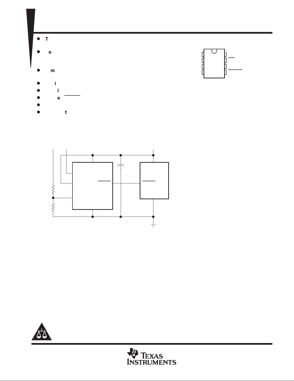
typical applications
Figure 1 lists some of the typical applications for the TPS3307 family, and a schematic diagram for a
processor-based system application. This application uses TI part numbers TPS3307–33 and MSP430C325.
3.3 V5 V2.5 V
• Applications using DSPs, Microcontrollers
or Microprocessors
• Industrial Equipment
• Programmable Controls
• Automotive Systems
• Portable/Battery Powered Equipment
• Intelligent Instruments
• Wireless Communication Systems
• Notebook/Desktop Computers
470 kΩ
620 kΩ
V
DD
SENSE 1
SENSE 2 RESET
TPS3307–33
SENSE 3
GND
100 nF
V
DD
MSP430C325
RESET
GND
Figure 1. Applications Using the TPS3307 Family
description
The TPS3307 family is a series of micropower supply voltage supervisors designed for circuit initialization
primarily in DSP and processor-based systems, which require more than one supply voltage.
The product spectrum of the TPS3307-xx is designed for monitoring three independent supply voltages:
3.3 V/1.8 V/adj, 3.3 V/2.5 V/adj or 3.3 V/5 V/adj. The adjustable SENSE input allows the monitoring of any supply
voltage >1.25 V.
The various supply voltage supervisors are designed to monitor the nominal supply voltage as shown in the
following supply voltage monitoring table.
Please be aware that an important notice concerning availability, standard warranty, and use in critical applications of
Texas Instruments semiconductor products and disclaimers thereto appears at the end of this data sheet.
PRODUCTION DATA information is current as of publication date.
Products conform to specifications per the terms of Texas Instruments
standard warranty. Production processing does not necessarily include
testing of all parameters.
POST OFFICE BOX 655303 • DALLAS, TEXAS 75265
Copyright 1998, Texas Instruments Incorporated
1
TPS3307-18, TPS3307-25, TPS3307-33
DEVICE
TRIPLE PROCESSOR SUPERVISORS
SLVS199 – DECEMBER 1998
description (continued)
SUPPLY VOLTAGE MONITORING
NOMINAL SUPERVISED VOLTAGE THRESHOLD VOLTAGE (TYP)
SENSE1 SENSE2 SENSE3 SENSE1 SENSE2 SENSE3
TPS3307-18 3.3 V 1.8 V User defined 2.93 V 1.68 V 1.25 V
TPS3307-25 3.3 V 2.5 V User defined 2.93 V 2.25 V 1.25 V
TPS3307-33 5 V 3.3 V User defined 4.55 V 2.93 V 1.25 V
†
The actual sense voltage has to be adjusted by an external resistor divider according to the application requirements.
†
†
†
During power-on, RESET is asserted when the supply voltage V
supply voltage supervisor monitors the SENSEn inputs
below the threshold voltage V
An internal timer delays the return of the RESET
The delay time, t
= 200 ms, starts after all SENSEn inputs have risen above the threshold voltage V
d typ
IT+
.
output to the inactive state (high) to ensure proper system reset.
and keeps RESET active as long as SENSEn remain
the voltage at any SENSE input drops below the threshold voltage V
becomes higher than 1.1 V . Thereafter , the
DD
, the RESET output becomes active (low)
IT–
IT+
. When
again.
The TPS3307-xx family of devices incorporates a manual reset input, MR
. A low level at MR causes RESET
to become active. In addition to the active-low RESET output, the TPS3307-xx family includes an active-high
RESET output.
The devices are available in either 8-pin MSOP or standard 8-pin SO packages.
The TPS3307-xx devices are characterized for operation over a temperature range of – 40°C to 85°C.
AVAILABLE OPTIONS
PACKAGED DEVICES
T
A
–40_C to 85_C
SMALL OUTLINE
(D)
TPS3307-18D TPS3307-18DGN TIAAP TPS3307-18Y
TPS3307-25D TPS3307-25DGN TIAAQ TPS3307-25Y
TPS3307-33D TPS3307-33DGN TIAAR TPS3307-33Y
PowerPAD
µ-SMALL OUTLINE
(DGN)
MARKING
DGN PACKAGE
CHIP FORM
(Y)
MR
L X
H 0 0 0 L H
H 0 0 1 L H
H 0 1 0 L H
H 0 1 1 L H
H 1 0 0 L H
H 1 0 1 L H
H 1 1 0 L H
H 1 1 1 H L
†
X = Don’t care
PowerPAD is a trademark of Texas Instruments Incorporated.
2
SENSE1>V
†
IT1
FUNCTION/TRUTH TABLES
SENSE2>V
POST OFFICE BOX 655303 • DALLAS, TEXAS 75265
IT2
†
X
SENSE3>V
IT3
X L H
RESET RESET
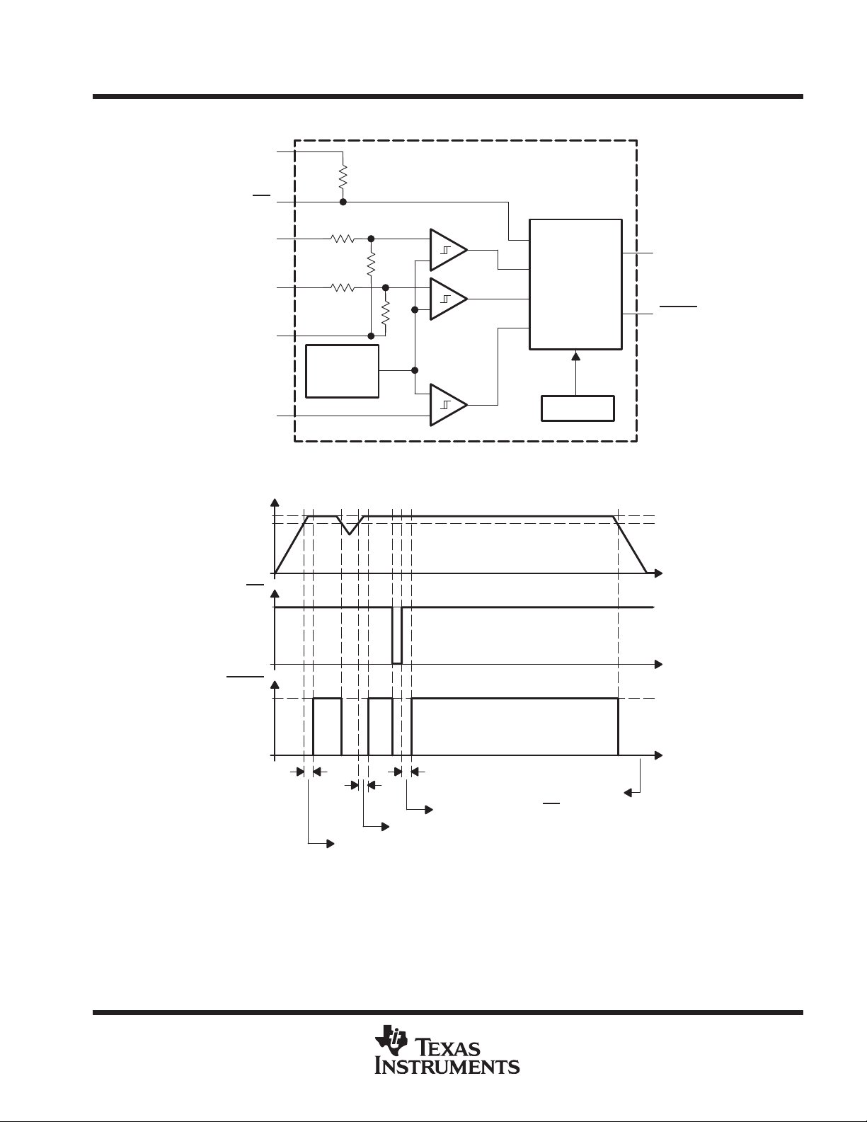
functional block diagram
V
DD
MR
SENSE 1
SENSE 2
GND
SENSE 3
14 kΩ
R1
R3
Reference
Voltage
of 1.25 V
R2
R4
+
_
+
_
_
+
TPS3307-18, TPS3307-25, TPS3307-33
TRIPLE PROCESSOR SUPERVISORS
SLVS199 – DECEMBER 1998
TPS3307
RESET
RESET
Logic + Timer
RESET
Oscillator
timing diagram
SENSEn
V
(nom)
V
IT–
MR
RESET
t
1
0
1
0
t
d
t
d
RESET Because of SENSE Below V
t
d
RESET Because of SENSE Below V
RESET Because of MR
RESET Because of SENSE Below V
IT–
IT
IT–
t
t
POST OFFICE BOX 655303 • DALLAS, TEXAS 75265
3
TPS3307-18, TPS3307-25, TPS3307-33
I/O
DESCRIPTION
TRIPLE PROCESSOR SUPERVISORS
SLVS199 – DECEMBER 1998
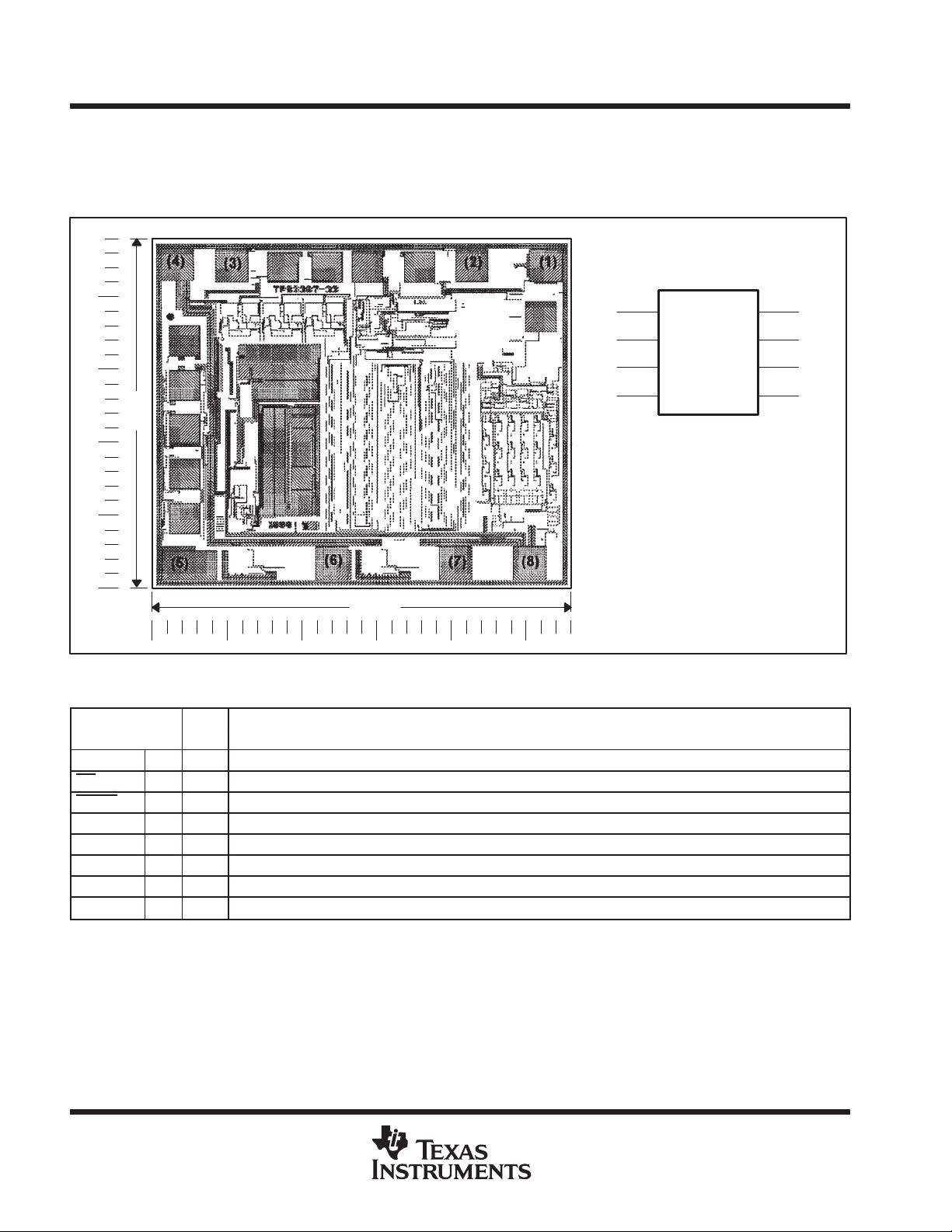
TPS3307Y chip information
These chips, when properly assembled, display characteristics similar to those of the TPS3307. Thermal
compression or ultrasonic bonding may take place on the doped aluminium bonding pads. The chips may be
mounted with conductive epoxy or a gold-silicon preform.
48
TERMINAL
NAME NO.
GND 4 Ground
MR 7 I Manual reset
RESET 5 O Active-low reset output
RESET 6 O Active-high reset output
SENSE1 1 I Sense voltage input 1
SENSE2 2 I Sense voltage input 2
SENSE3 3 I Sense voltage input 3
V
DD
8 Supply voltage
56
Terminal Functions
(1)
(2)
TPS3307Y
(3)
(4)
CHIP THICKNESS: 10 TYPICAL
BONDING PADS: 4 × 4 MINIMUM
TJ max = 150°C
TOLERANCES ARE ±10%.
ALL DIMENSIONS ARE IN MILS
(8)
(7)
(6)
(5)
4
POST OFFICE BOX 655303 • DALLAS, TEXAS 75265

TPS3307-18, TPS3307-25, TPS3307-33
TRIPLE PROCESSOR SUPERVISORS
SLVS199 – DECEMBER 1998
absolute maximum ratings over operating free-air temperature range (unless otherwise noted)
Supply voltage, V
(see Note1) 7 V. . . . . . . . . . . . . . . . . . . . . . . . . . . . . . . . . . . . . . . . . . . . . . . . . . . . . . . . . . . . .
DD
†
All other pins (see Note 1) –0.3 V to 7 V. . . . . . . . . . . . . . . . . . . . . . . . . . . . . . . . . . . . . . . . . . . . . . . . . . . . . . . . . .
Maximum low output current, I
Maximum high output current, I
Input clamp current, I
Output clamp current, I
IK
(V
OK
I
(V
5 mA. . . . . . . . . . . . . . . . . . . . . . . . . . . . . . . . . . . . . . . . . . . . . . . . . . . . . . . . . . .
OL
–5 mA. . . . . . . . . . . . . . . . . . . . . . . . . . . . . . . . . . . . . . . . . . . . . . . . . . . . . . . . .
OH
< 0 or V
O
> VDD) ±20 mA. . . . . . . . . . . . . . . . . . . . . . . . . . . . . . . . . . . . . . . . . . . . . . . .
I
< 0 or V
> VDD) ±20 mA. . . . . . . . . . . . . . . . . . . . . . . . . . . . . . . . . . . . . . . . . . . .
O
Continuous total power dissipation See Dissipation Rating Table. . . . . . . . . . . . . . . . . . . . . . . . . . . . . . . . . . . . .
Operating free-air temperature range, T
Storage temperature range, T
–65°C to 150°C. . . . . . . . . . . . . . . . . . . . . . . . . . . . . . . . . . . . . . . . . . . . . . . . . . .
stg
–40°C to 85°C. . . . . . . . . . . . . . . . . . . . . . . . . . . . . . . . . . . . . . . . . . .
A
Soldering temperature 260_C. . . . . . . . . . . . . . . . . . . . . . . . . . . . . . . . . . . . . . . . . . . . . . . . . . . . . . . . . . . . . . . . . . . .
†
Stresses beyond those listed under “absolute maximum ratings” may cause permanent damage to the device. These are stress ratings only, and
functional operation of the device at these or any other conditions beyond those indicated under “recommended operating conditions” is not
implied. Exposure to absolute-maximum-rated conditions for extended periods may affect device reliability.
NOTE 1: All voltage values are with respect to GND. For reliable operation the device must not be operated at 7 V for more than t = 1000 h
continuously.
DISSIPATION RATING TABLE
PACKAGE
DGN 2.14 mW 17.1 mW/°C 1.37 mW 1.11 mW
D 725 mW 5.8 mW/°C 464 mW 377 mW
TA ≤ 25°C
POWER RATING
DERATING FACTOR
ABOVE TA = 25°C
TA = 70°C
POWER RATING
TA = 85°C
POWER RATING
recommended operating conditions at specified temperature range
MIN MAX UNIT
Supply voltage, V
Input voltage at MR and SENSE3, V
Input voltage at SENSE1 and SENSE2, V
High-level input voltage at MR, V
Low-level input voltage at MR, V
Input transition rise and fall rate at MR, ∆t/∆V 50 ns/V
Operating free-air temperature range, T
DD
I
I
IH
IL
A
2 6 V
0 VDD+0.3 V
0 (VDD+0.3)VIT/1.25V V
0.7xV
DD
0.3×V
DD
–40 85 °C
V
V
POST OFFICE BOX 655303 • DALLAS, TEXAS 75265
5

TPS3307-18, TPS3307-25, TPS3307-33
V
V
ggg g
V
y
y
IHHigh-level input current
A
ILLow-level input current
A
TRIPLE PROCESSOR SUPERVISORS
SLVS199 – DECEMBER 1998
electrical characteristics over recommended operating free-air temperature range (unless
otherwise noted)
PARAMETER TEST CONDITIONS MIN TYP MAX UNIT
VDD = 2 V to 6 V, IOH = –20 µA VDD– 0.2V
V
High-level output voltage
OH
V
Low-level output voltage
OL
Power-up reset voltage (see Note 2) VDD ≥ 1.1 V, IOL = 20 µA 0.4 V
VSENSE3
VSENSE1,
VSENSE2
Negative-going input threshold voltage
IT–
(see Note 3)
V
Hysteresis at VSENSEn input
h
s
p
p
I
Supply current 40 µΑ
DD
C
Input capacitance VI = 0 V to V
i
NOTES: 2. The lowest supply voltage at which RESET becomes active. tr, VDD ≥ 15 µs/V
3. T o ensure best stability of the threshold voltage, a bypass capacitor (ceramic 0.1 µF) should be placed close to the supply terminals.
VSENSE3
VSENSE1,
VSENSE2
MR MR = 0.7 × V
SENSE1 VSENSE1 = VDD = 6 V 5 8
SENSE2 VSENSE2 = VDD = 6 V 6 9
SENSE3 VSENSE3 = V
MR MR = 0 V, VDD = 6 V –430 –600
SENSEn VSENSE1,2,3 = 0 V –1 1
VDD = 3.3 V, IOH = –2 mA
VDD = 6 V, IOH = –3 mA VDD– 0.4V
VDD = 2 V to 6 V, IOL = 20 µA 0.2
VDD = 3.3 V, IOL = 2 mA 0.4 V
VDD = 6 V, IOL = 3 mA 0.4
VDD = 2 V to 6 V,
TA = 0°C to 85°C
VDD = 2 V to 6 V,
TA = –40°C to 85°C
V
= 1.25 V 10
IT–
V
= 1.68 V 15
IT–
V
= 2.25 V
IT–
V
= 2.93 V 30
IT–
V
= 4.55 V 40
IT–
DD,VDD
DD
DD
= 6 V –130 –180
VDD– 0.4V
1.22 1.25 1.28
1.64 1.68 1.72
2.20 2.25 2.30
2.86 2.93 3
4.46 4.55 4.64
1.22 1.25 1.29 V
1.64 1.68 1.73
2.20 2.25 2.32
2.86 2.93 3.02
4.46 4.55 4.67
20
–1 1
10 pF
V
mV
µ
µ
6
POST OFFICE BOX 655303 • DALLAS, TEXAS 75265

twPulse width
)
I(SENSEn) IT+
200
500
ns
IH IT+ IL IT
1
5µs
TPS3307-18, TPS3307-25, TPS3307-33
TRIPLE PROCESSOR SUPERVISORS
SLVS199 – DECEMBER 1998
timing requirements at V
PARAMETER TEST CONDITIONS MIN TYP MAX UNIT
SENSEn V
MR VIH = 0.7 × VDD,V
= 2 V to 6 V, R
DD
switching characteristics at V
PARAMETER TEST CONDITIONS MIN TYP MAX UNIT
t
d
t
PHL
t
PLH
t
PHL
t
PLH
Delay time
Propagation (delay) time,
high-to-low level output
Propagation (delay) time,
low-to-high level output
Propagation (delay) time,
high-to-low level output
Propagation (delay) time,
low-to-high level output
SENSEnL
DD
MR to RESET
MR to RESET
MR to RESET
MR to RESET
SENSEn to RESET
SENSEn to RESET
SENSEn to RESET
SENSEn to RESET
= V
IT–
= 2 V to 6 V, R
= 1 MΩ, C
L
–0.2 V, V
= 1 MΩ, C
L
V
I(SENSEn)
≥ 0.7 × VDD, See timing diagram
MR
V
I(SENSEn
VIH = 0.7 × VDD,VIL = 0.3 × V
VIH = V
MR ≥ 0.7 × V
= 50 pF, T
L
SENSEnH
= 0.3 × V
IL
≥ V
≥ V
+0.2 V, VIL = V
IT+
DD
= V
IT+
IT+
= 25°C
A
+0.2 V 6 µs
IT+
DD
= 50 pF, T
L
+ 0.2 V,
+0.2 V,
IT–
DD
–0.2 V,
100 ns
= 25°C
A
140 200 280 ms
POST OFFICE BOX 655303 • DALLAS, TEXAS 75265
7

TPS3307-18, TPS3307-25, TPS3307-33
TRIPLE PROCESSOR SUPERVISORS
SLVS199 – DECEMBER 1998
TYPICAL CHARACTERISTICS
NORMALIZED SENSE THRESHOLD VOLTAGE
C
°
1.005
1.004
1.003
1.002
1.001
1
0.999
0.998
0.997
0.996
0.995
–40 –15 10 35
Normalized Input Threshold Voltage – VIT(TA), VIT(25 )
100
VDD = 6 V
TA = 25°C
0
–100
Aµ
–200
–300
–400
–500
– Input Current –
I
I
–600
vs
FREE-AIR TEMPERATURE AT V
VDD = 2 V
MR
= Open
60 85
TA – Free-Air Temperature – ° C
Figure 2
INPUT CURRENT
vs
INPUT VOLTAGE AT MR
DD
18
16
14
12
Aµ
10
8
6
4
2
0
– Supply Current –
–2
DD
I
–4
–6
–8
–10
–0.5 0 0.5 1 2.5 3 3.5
1.5 2 4.5 5.5 6.5
VDD – Supply Voltage – V
MINIMUM PULSE DURATION AT SENSE
THRESHOLD OVERDRIVE
10
sµ
9
8
sense –
V
7
6
5
4
3
SUPPLY CURRENT
vs
SUPPLY VOLTAGE
TPS3307–33
SENSEn = V
MR
TA = 25°C
4567
Figure 3
vs
= Open
VDD = 6 V
MR
= Open
DD
–700
–800
–900
–1–0.5 0 1 1.5 2.5 3
0.5 2
V
– Input Voltage at MR
I
4.5
3.5 4 5.5 6.5
56
– V
Figure 4
8
POST OFFICE BOX 655303 • DALLAS, TEXAS 75265
2
– Minimum Pulse Duration at
1
w
t
0
0 100 200 300 400 500 600
SENSE – Threshold Overdrive – mV
Figure 5
700 800 900 1000

TPS3307-18, TPS3307-25, TPS3307-33
TRIPLE PROCESSOR SUPERVISORS
SLVS199 – DECEMBER 1998
TYPICAL CHARACTERISTICS
HIGH-LEVEL OUTPUT VOLTAGE
HIGH-LEVEL OUTPUT CURRENT
2.5
VDD = 2 V
MR
= Open
2
1.5
1
– High-Level Output Voltage – V
0.5
OH
V
0
0 –0.5 –1 –1.5 –2 –2.5 –3
IOH – High-Level Output Current – mA
LOW-LEVEL OUTPUT VOLTAGE
LOW-LEVEL OUTPUT CURRENT
2.5
VDD = 2 V
MR
= Open
2
1.5
1
– Low-Level Output Voltage – V
0.5
OL
V
0
0 0.5 1 1.5 2 3 3.5
IOL – Low-Level Output Current – mA
vs
85°C
Figure 6
vs
85°C
2.5
Figure 8
–40°C
–3.5 –4 –5 –6–4.5 –5.5
–40°C
4 4.5 5.5 6
5
HIGH-LEVEL OUTPUT VOLTAGE
HIGH-LEVEL OUTPUT CURRENT
6.5
6
5.5
5
4.5
4
3.5
3
2.5
2
– High-Level Output Voltage – V
1.5
OH
1
V
0.5
0
0 –5 –10 –15 –20 –25 –30
IOH – High-Level Output Current – mA
LOW-LEVEL OUTPUT VOLTAGE
LOW-LEVEL OUTPUT CURRENT
6.5
VDD = 6 V
6
MR
5.5
5
4.5
4
3.5
3
2.5
2
– Low-Level Output Voltage – V
1.5
OL
V
1
0.5
0
= Open
0 5 10 15 20 30 35
IOL – Low-Level Output Current – mA
vs
85°C
Figure 7
vs
85°C
25 45
Figure 9
VDD = 6 V
MR
= Open
–40°C
–35 –40 –45 –50
–40°C
40 50 55 60
POST OFFICE BOX 655303 • DALLAS, TEXAS 75265
9
TPS3307-18, TPS3307-25, TPS3307-33
TRIPLE PROCESSOR SUPERVISORS
SLVS199 – DECEMBER 1998
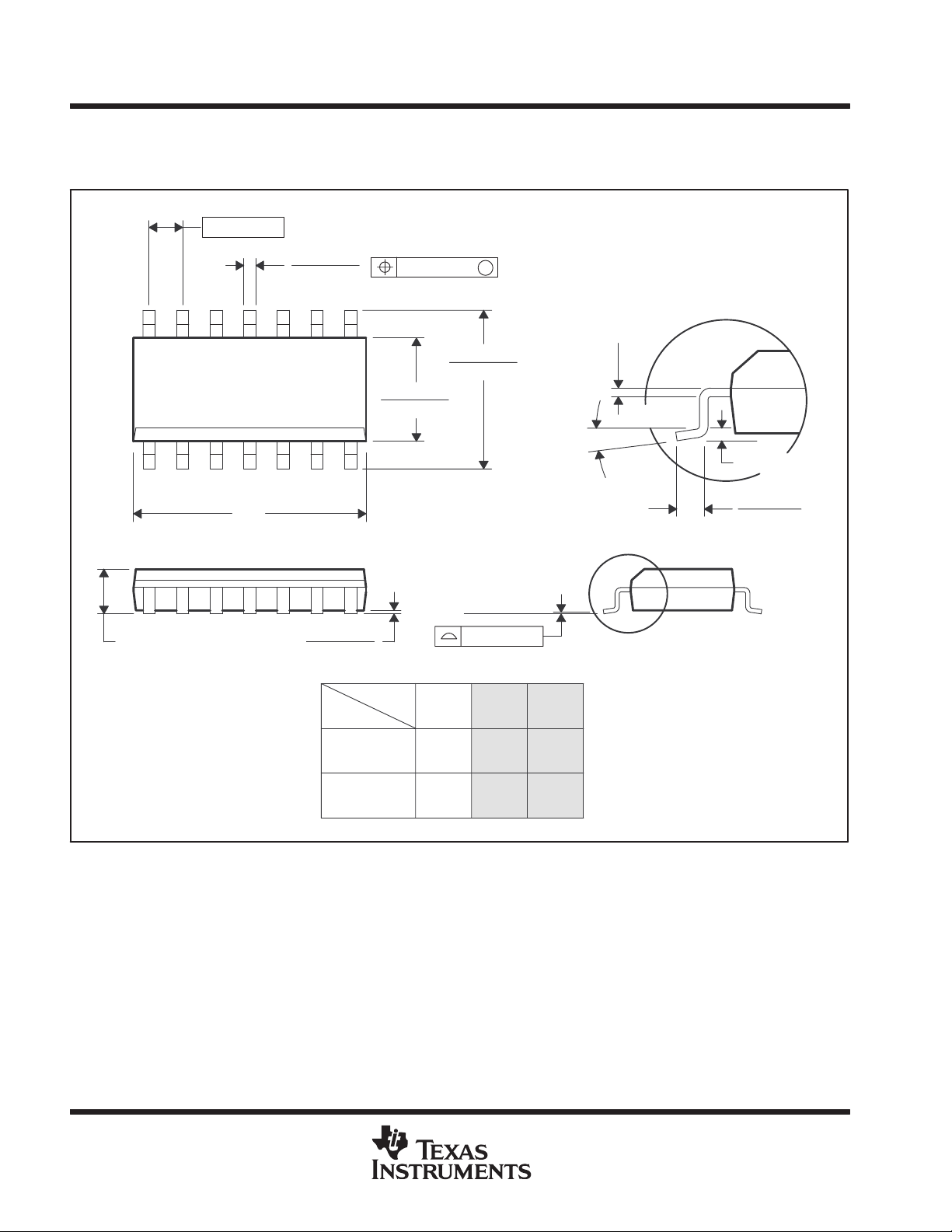
MECHANICAL DATA
D (R-PDSO-G**) PLASTIC SMALL-OUTLINE PACKAGE
14 PIN SHOWN
0.050 (1,27)
14
1
0.069 (1,75) MAX
A
0.020 (0,51)
0.014 (0,35)
0.010 (0,25)
0.004 (0,10)
DIM
8
7
PINS **
0.010 (0,25)
0.157 (4,00)
0.150 (3,81)
M
0.244 (6,20)
0.228 (5,80)
Seating Plane
0.004 (0,10)
8
14
0.008 (0,20) NOM
0°–8°
16
Gage Plane
0.010 (0,25)
0.044 (1,12)
0.016 (0,40)
A MAX
A MIN
NOTES: A. All linear dimensions are in inches (millimeters).
10
B. This drawing is subject to change without notice.
C. Body dimensions do not include mold flash or protrusion, not to exceed 0.006 (0,15).
D. Falls within JEDEC MS-012
POST OFFICE BOX 655303 • DALLAS, TEXAS 75265
0.197
(5,00)
0.189
(4,80)
0.344
(8,75)
0.337
(8,55)
0.394
(10,00)
0.386
(9,80)
4040047/D 10/96

TPS3307-18, TPS3307-25, TPS3307-33
TRIPLE PROCESSOR SUPERVISORS
SLVS199 – DECEMBER 1998
MECHANICAL DATA
DGN (S-PDSO-G8) PowerPAD PLASTIC SMALL-OUTLINE PACKAGE
0,65
8
1
1,07 MAX
3,05
2,95
0,38
0,25
5
3,05
2,95
4
Seating Plane
0,15
0,05
0,25
4,98
4,78
M
0,10
Thermal Pad
(See Note D)
0,15 NOM
0°–6°
Gage Plane
0,25
0,69
0,41
NOTES: A. All linear dimensions are in millimeters.
B. This drawing is subject to change without notice.
C. Body dimensions include mold flash or protrusions.
D. The package thermal performance may be enhanced by attaching an external heat sink to the thermal pad. This pad is electrically
and thermally connected to the backside of the die and possibly selected leads.
E. Falls within JEDEC MO-187
PowerPAD is a trademark of Texas Instruments Incorporated.
4073271/A 01/98
POST OFFICE BOX 655303 • DALLAS, TEXAS 75265
11

IMPORTANT NOTICE
T exas Instruments and its subsidiaries (TI) reserve the right to make changes to their products or to discontinue
any product or service without notice, and advise customers to obtain the latest version of relevant information
to verify, before placing orders, that information being relied on is current and complete. All products are sold
subject to the terms and conditions of sale supplied at the time of order acknowledgement, including those
pertaining to warranty, patent infringement, and limitation of liability.
TI warrants performance of its semiconductor products to the specifications applicable at the time of sale in
accordance with TI’s standard warranty. Testing and other quality control techniques are utilized to the extent
TI deems necessary to support this warranty . Specific testing of all parameters of each device is not necessarily
performed, except those mandated by government requirements.
CERT AIN APPLICATIONS USING SEMICONDUCTOR PRODUCTS MA Y INVOLVE POTENTIAL RISKS OF
DEATH, PERSONAL INJURY, OR SEVERE PROPERTY OR ENVIRONMENTAL DAMAGE (“CRITICAL
APPLICATIONS”). TI SEMICONDUCTOR PRODUCTS ARE NOT DESIGNED, AUTHORIZED, OR
WARRANTED TO BE SUITABLE FOR USE IN LIFE-SUPPORT DEVICES OR SYSTEMS OR OTHER
CRITICAL APPLICA TIONS. INCLUSION OF TI PRODUCTS IN SUCH APPLICATIONS IS UNDERST OOD TO
BE FULLY AT THE CUSTOMER’S RISK.
In order to minimize risks associated with the customer’s applications, adequate design and operating
safeguards must be provided by the customer to minimize inherent or procedural hazards.
TI assumes no liability for applications assistance or customer product design. TI does not warrant or represent
that any license, either express or implied, is granted under any patent right, copyright, mask work right, or other
intellectual property right of TI covering or relating to any combination, machine, or process in which such
semiconductor products or services might be or are used. TI’s publication of information regarding any third
party’s products or services does not constitute TI’s approval, warranty or endorsement thereof.
Copyright 1998, Texas Instruments Incorporated
 Loading...