

M1
R
CS
C
OUT
D
VC1
GATE
ARTN
V
C
CS
C
VC
CTL
V
B
D
1
C
1
R
DEN
From Ethernet
Pairs 1,2
V
SS
C
IN
R
CTL
C
CTL
From Ethernet
Pairs 3,4
CLS
DEN
FRS
T2P
R
CLS
R
T2P-OUT
Type2PSE
Indicator
R
FRS
V
B
C
VB
R
FBU
R
FBL
TLV431
R
OB
C
IZ
V
OUT
PAD
V
DD1
GAT2
M2
D
CL
C
CL
C
C
M4
M3
R
T2P
D
A
R
APD2
R
APD1
N/CORPPD
Adapter
DT
R
BLNK
APD
R
DT
BLNK
V
DD
RTN
COM
L
OUT
L
VC
T1
C
IO
D
VC2
Optional
Interface
V
T2P-OUT
www.ti.com
....................................................................................................................................................... SLVS885B – OCTOBER 2008 – REVISED MAY 2009
High Power/High Efficiency PoE Interface and DC/DC Controller
1
FEATURES
2
• Powers up to 30 W (input) PDs
• DC/DC Control Optimized for Isolated
Converters
• Supports High-efficiency Topologies
• Complete PoE Interface
• Enhanced Classification per IEEE 802.3at
(Draft) with Status Flag
• Adapter ORing Support
• Programmable Frequency with
Synchronization
• Robust 100 V, 0.5 Ω Hotswap MOSFET
• – 40 ° C to 125 ° C Junction Temperature Range
• Industry Standard PowerPAD™ TSSOP-20
APPLICATIONS
• IEEE 802.3at (Draft) Compliant Devices
• Video and VoIP Telephones
• RFID Readers
• Multiband Access Points
• Security Cameras
DESCRIPTION
The TPS23754/6 is a combined Power over Ethernet
(PoE) powered device (PD) interface and
current-mode dc/dc controller optimized specifically
for isolated converters. The PoE interface supports
the IEEE 802.3at (draft) standard.
TPS23754
TPS23754-1
TPS23756
The TPS23754/6 supports a number of input voltage
ORing options including highest voltage, external
adapter preference, and PoE preference. These
features allow the designer to determine which power
source will carry the load under all conditions.
The PoE interface features the new extended
hardware classification necessary for compatibility
with high-power midspan power sourcing equipment
(PSE) per IEEE 802.3at (draft). The detection
signature pin can also be used to force power from
the PoE source off. Classification can be
programmed to any of the defined types with a single
resistor.
The dc/dc controller features two complementary gate
drivers with programmable dead time. This simplifies
design of active-clamp forward converters or
optimized gate drive for highly-efficient flyback
topologies. The second gate driver may be disabled if
desired for single MOSFET topologies. The controller
also features internal softstart, bootstrap startup
source, current-mode compensation, 78% maximum
duty cycle. A programmable and synchronizable
oscillator allows design optimization for efficiency and
eases use of the controller to upgrade existing power
supply designs. Accurate programmable blanking,
with a default period, simplifies the usual
current-sense filter design trade-offs.
The TPS23754 has a 15 V converter startup while the
TPS23756 has a 9 V converter startup. The
TPS23754-1 replaces the PPD pin with a no-connect
for increased pin spacing.
1
2 PowerPAD is a trademark of Texas Instruments.
PRODUCTION DATA information is current as of publication date.
Products conform to specifications per the terms of the Texas
Instruments standard warranty. Production processing does not
necessarily include testing of all parameters.
Please be aware that an important notice concerning availability, standard warranty, and use in critical applications of Texas
Instruments semiconductor products and disclaimers thereto appears at the end of this data sheet.
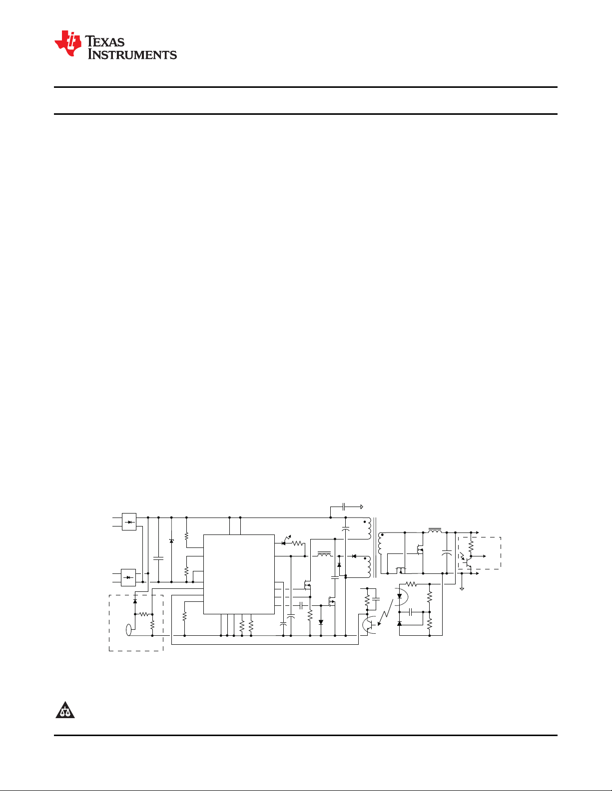
Figure 1. High Efficiency Converter Using TPS23754
Copyright © 2008 – 2009, Texas Instruments Incorporated
TPS23754
TPS23754-1
TPS23756
SLVS885B – OCTOBER 2008 – REVISED MAY 2009 .......................................................................................................................................................
This device contains circuits to protect its inputs and outputs against damage due to high static voltages or electrostatic fields.
These circuits have been qualified to protect this device against electrostatic discharges (ESD) of up to 2 kV according to
MIL-STD-883C, Method 3015; however, it is advised that precautions be taken to avoid application of any voltage higher than
maximum-rated voltages to these high-impedance circuits. During storage or handling the device leads should be shorted together
or the device should be placed in conductive foam. In a circuit, unused inputs should always be connected to an appropriate
voltage level, preferably either the proper supply or ground. Specific guidelines for handling devices of this type are contained in
the publication Guidelines for Handling Electrostatic-Discharge-Sensitive (ESDS) Devices and Assemblies available from Texas
Instruments.
www.ti.com
PRODUCT INFORMATION
STATUS FEATURE PACKAGE MARKING
DUTY POE UVLO CONVERTER UVLO
CYCLE ON / HYST. ON / HYST.
(1)
TPS23754PWP Active 0 – 78% 35/4.5 15 / 6.5 PPD TSSOP-20 TPS23754
PowerPAD™
TPS23754PWP-1 Active 0 – 78% 35/4.5 15 / 6.5 – TSSOP-20 23754-1
PowerPAD™
TPS23756PWP Active 0 – 78% 35/4.5 9 / 3.5 PPD TSSOP-20 TPS23756
PowerPAD™
(1) For the most current package and ordering information, see the Package Option Addendum at the end of this document, or see the TI
web site at www.ti.com .
ABSOLUTE MAXIMUM RATINGS
Voltage with respect to V
unless otherwise noted.
SS
(1) (2)
VALUE UNIT
Input voltage range, ARTN
Input voltage range CLS
(2)
(4)
Input voltage range [APD, BLNK
Input voltage range CS to [ARTN,COM] – 0.3 to V
(2)
, COM
, DEN, PPD, RTN
(3)
, VDD, V
DD1
– 0.3 to 100 V
-0.3 to 6.5 V
(4)
, CTL, DT
(4)
(4)
, FRS
(4)
, VB
] to [ARTN, COM] – 0.3 to 6.5 V
B
Input voltage range [ARTN, COM] to RTN – 2 to 2 V
Voltage range VC, T2P, to [ARTN, COM] – 0.3 to 19 V
Voltage range GATE
(4)
(4)
, GAT2
to [ARTN, COM] – 0.3 to VC+0.3 V
Sinking current RTN Internally limited mA
Sourcing current V
B
Internally limited mA
Average Sourcing or sinking current, GATE, GAT2 25 mArms
ESD rating, HBM 2 kV
ESD rating, CDM 500 V
ESD – system level (contact/air) at RJ-45
Operating junction temperature range, T
(5)
J
– 40 to Internally limited ° C
8 / 15 kV
(1) Stresses beyond those listed under absolute maximum ratings may cause permanent damage to the device. These are stress ratings
only and functional operation of the device at these or any other conditions beyond those indicated under recommended operating
conditions is not implied. Exposure to absolute-maximum-rated conditions for extended periods may affect device reliability.
(2) ARTN and COM must be tied to RTN.
(3) I
(4) Do not apply voltage to these pins
= 0 for V
RTN
> 80V.
RTN
(5) ESD per EN61000-4-2. A power supply containing the TPS23754 was subjected to the highest test levels in the standard. See the ESD
section.
V
2 Submit Documentation Feedback Copyright © 2008 – 2009, Texas Instruments Incorporated
Product Folder Link(s): TPS23754 TPS23754-1 TPS23756
TPS23754
TPS23754-1
TPS23756
www.ti.com
....................................................................................................................................................... SLVS885B – OCTOBER 2008 – REVISED MAY 2009
RECOMMENDED OPERATING CONDITIONS
Voltage with respect to V
(unless otherwise noted)
SS
(1)
MIN NOM MAX UNIT
Input voltage range ARTN, COM, PPD, RTN, VDD, V
DD1
0 57 V
Input voltage range T2P, VCto [ARTN, COM] 0 18 V
Input voltage range APD, CTL, DT to [ARTN, COM] 0 V
B
Input voltage range CS to [ARTN, COM] 0 2 V
Continuous RTN current (T
Sourcing current, V
B
J
≤ 125 ° C)
(2)
825 mA
0 2.5 5 mA
VBcapacitance 0.08 µ F
R
BLNK
0 350 k Ω
Synchronization pulse width input (when used) 25 ns
Operating junction temperature range, T
J
– 40 125 ° C
(1) ARTN and COM tied to RTN.
(2) This is the minimum current-limit value. Viable systems will be designed for maximum currents below this value with reasonable margin.
IEEE 802.3at (draft) permits 600mA continuous loading
DISSIPATION RATINGS
Ψ
PACKAGE
JT
(1)
° C/W
PWP (TSSOP-20) 0.607 1.4 32.6 73.8 1.2
(1) Thermal resistance junction to case top.
(2) See TI document SLMA002 C (or latest version) for recommended layout. This is a best case, natural convection number.
(3) JEDEC method with high-k board (2 signal – 2 plane layers) and power pad not soldered (worst case).
(4) Based on TI recommended layout and 85 ° C.
θ
JP
° C/W ° C/W
θ
JA
(2)
θ
JA
(3)
° C/W
MAXIMUM POWER RATING
(4)
(W)
V
ELECTRICAL CHARACTERISTICS
Unless otherwise noted: CS=COM=APD=CTL=RTN=ARTN, GATE & GAT2 float, R
PPD=V
125 ° C. Typical specifications are at 25 ° C.
CONTROLLER SECTION ONLY
[V
V
V
V
t
ST
V
(1) The hysteresis tolerance tracks the rising threshold for a given device.
SS
= RTN and V
SS
C
CUV
CUVH
B
, T2P open, C
=C
=0.1 µ F, R
VB
VC
=V
DD
] or [V
DD1
SS
=RTN=V
=24.9 k Ω , R
DEN
open, 0 V ≤ (V
CLS
], all voltages referred to [ARTN, COM].
DD
, V
DD
PARAMETER TEST CONDITIONS MIN TYP MAX UNIT
VCrising ‘ 754 14.3 15 15.7
UVLO V
Operating current VC= 12 V, CTL = VB, R
Bootstrap startup time,
C
= 22 µ F
VC
Startup current source - I
VC
VCrising ‘ 756 8.7 9 9.3
Hysteresis ‘ 754
Hysteresis ‘ 756
‘ 756, V
DD1
‘ 756, V
DD1
‘ 754, V
DD1
‘ 754, V
DD1
‘ 754, V
DD1
‘ 756, V
DD1
‘ 754, ‘ 756, V
(1)
(1)
= 68.1 k Ω 0.7 0.92 1.2 mA
DT
= 10.2 V, VC(0) = 0 V 50 85 175
= 35 V, VC(0) = 0 V 27 45 92
= 19.2 V, VC(0) = 0 V 49 81 166
= 35 V, VC(0) = 0 V 44 75 158
= 19.2 V, VC= 13.9 V 1.7 3.4 5.5
= 10.2 V, VC= 8.6 V 0.44 1.06 1.80 mA
= 48 V, VC= 0 V 2.7 4.8 6.8
DD1
Voltage 6.5 V ≤ VC≤ 18 V, 0 ≤ IVB≤ 5 mA 4.8 5.10 5.25 V
=68.1 k Ω , R
FRS
) ≤ 57 V, 0 V ≤ VC≤ 18 V, – 40 ° C ≤ T
DD1
=249 k Ω , DT=V
BLNK
6.2 6.5 6.8
3.3 3.5 3.7
,
B
≤
J
ms
Copyright © 2008 – 2009, Texas Instruments Incorporated Submit Documentation Feedback 3
Product Folder Link(s): TPS23754 TPS23754-1 TPS23756
TPS23754
TPS23754-1
TPS23756
SLVS885B – OCTOBER 2008 – REVISED MAY 2009 .......................................................................................................................................................
PARAMETER TEST CONDITIONS MIN TYP MAX UNIT
FRS
Switching frequency kHz
D
MAX
V
SYNC
Duty cycle CTL= VB, measure GATE 76 78 80 %
Synchronization Input threshold 2 2.2 2.4 V
CTL
V
ZDC
0% duty cycle threshold V
Softstart period Interval from switching start to V
Input resistance 70 100 145 k Ω
BLNK
Blanking delay
(In addition to t1)
DT
t
DT1
t
DT2
t
DT1
t
DT2
Dead time
See Figure 2 for t
definition R
DTx
CS
V
CSMAX
t
1
V
SLOPE
I
SL_EX
Maximum threshold voltage V
Turnoff delay V
Internal slope compensation
voltage
Peak slope compensation
current
Bias current (sourcing) DC component of I
GATE
Source current V
Sink current V
GAT2
Source current 0.37 0.6 0.95 A
Sink current 0.7 1.0 1.4 A
APD / PPD
V
APDEN
V
APDH
V
PPDEN
V
PPDH
V
PPD2
V
PPD2H
APD threshold voltage V
PPD threshold voltage
APD leakage current
(source or sink)
I
PPD
PPD sink current V
THERMAL SHUTDOWN
Turnoff temperature TJrising 135 145 155 ° C
Hysteresis
(3)
(2) The hysteresis tolerance tracks the rising threshold for a given device.
(3) These parameters are provided for reference only, and do not constitute part of TI ' s published specifications for purposes of TI ' s product
warranty.
CTL = VB, measure GATE
R
= 68.1 k Ω 227 253 278
FRS
↓ until GATE stops 1.3 1.5 1.7 V
CTL
CSMAX
1.9 3.9 6.2 ms
BLNK = RTN 35 55 78
R
= 49.9 k Ω 38 55 70
BLNK
CTL = VB, C
C
= 1 nF, measure GATE, GAT2
GAT2
R
= 24.9 k Ω , GAT2 ↑ to GATE ↑ 40 50 62.5
DT
= 24.9 k Ω , GATE ↓ to GAT2 ↓ 40 50 62.5
DT
R
= 75 k Ω , GAT2 ↑ to GATE ↑ 120 150 188
DT
R
= 75 k Ω , GATE ↓ to GAT2 ↓ 120 150 188
DT
= VB, V
CTL
= 0.65 V 24 40 70 ns
CS
= 1 nF,
GATE
rising until GATE duty cycle drops 0.5 0.55 0.6 V
CS
Peak voltage at maximum duty cycle, referenced to CS 120 155 185 mV
V
= VB, ICSat maximum duty cycle 30 42 54 µ A
CTL
CS
= VB, VC= 12 V, GATE high, pulsed measurement 0.37 0.6 0.95 A
CTL
= VB, VC= 12 V, GATE low, pulsed measurement 0.7 1.0 1.4 A
CTL
V
= VB, VC= 12 V, GAT2 high, R
CTL
measurement
V
= VB, VC= 12 V, GAT2 low, R
CTL
measurement
V
rising 1.43 1.5 1.57
APD
Hysteresis
V
PPD
Hysteresis
V
PPD
Hysteresis
VC= 12 V, V
PPD-VSS
(2)
- V
rising, UVLO disable 1.45 1.55 1.65
VSS
(2)
- V
rising, Class enable 7.4 8.3 9.2
VSS
(2)
= V
APD
B
= 1.5 V 2.5 5 7.5 µ A
= 24.9 k Ω , pulsed
DT
= 24.9 k Ω , pulsed
DT
1 2.5 4.3 µ A
0.29 0.31 0.33
0.29 0.31 0.33
0.5 0.6 0.7
20 ° C
www.ti.com
ns
ns
V
V
1 µ A
4 Submit Documentation Feedback Copyright © 2008 – 2009, Texas Instruments Incorporated
Product Folder Link(s): TPS23754 TPS23754-1 TPS23756
www.ti.com
....................................................................................................................................................... SLVS885B – OCTOBER 2008 – REVISED MAY 2009
ELECTRICAL CHARACTERISTICS – PoE AND CONTROL
[V
=V
DD
] or [V
DD1
DETECTION (DEN) (VDD = VDD1 = RTN = V
Detection current V
Detection bias current 5.6 10 µ A
V
PD_DIS
Hotswap disable threshold 3 4 5 V
DEN leakage current V
CLASSIFICATION (CLS) (V
I
CLS
Classification current,
applies to both cycles
Classification mark resistance 5.6 V ≤ V
V
CL_ON
V
CL_H
V
CU_OFF
V
CU_H
V
MSR
Classification regulator lower
threshold
Classification regulator upper
threshold
Mark state reset V
Leakage current V
PASS DEVICE (RTN) (V
On resistance 0.25 0.43 0.75 Ω
Current limit V
Inrush limit V
Foldback voltage threshold V
UVLO
V
UVLO_R
V
UVLO_H
UVLO threshold V
T2P
ON characteristic 2 mA
Leakage current V
t
T2P
Delay From start of switching to T2P active 5 9 15 ms
THERMAL SHUTDOWN
Turnoff temperature TJrising 135 145 155 ° C
Hysteresis
(1) The hysteresis tolerance tracks the rising threshold for a given device.
(2) These parameters are provided for reference only, and do not constitute part of TI ' s published specifications for purposes of TI ' s product
warranty.
=RTN], VC= RTN, COM=RTN=ARTN, all voltages referred to V
DD1
unless otherwise noted
SS
PARAMETER TEST CONDITIONS MIN TYP MAX UNIT
positive)
SUPPLY
Measure I
DD
V
DD
V
DD
Note: Not during Mark state
DEN
13 V ≤ V
R
CLS
R
CLS
R
CLS
R
CLS
R
CLS
Regulator turns on, V
Hysteresis
Regulator turns off, V
Hysteresis
DD
DD
RTN
RTN
DD
V
DD
Hysteresis
Perform classification algorithm, V
CTL = ARTN
T2P
(2)
SUPPLY
= 1.6 V 62 64.3 66.5
= 10 V 399 406 414
= 10 V, float DEN, measure I
= V
= 57 V, float V
DD
= V
DD
= RTN = V
DD1
≤ 21 V, Measure I
DD
SUPPLY
and RTN, measure I
DD1
positive)
SUPPLY
,
SUPPLY
DEN
0.1 5 µ A
= 1270 Ω 1.8 2.1 2.4
= 243 Ω 9.9 10.4 10.9
= 137 Ω 17.6 18.5 19.4
= 90.9 Ω 26.5 27.7 29.3
= 63.4 Ω 38.0 39.7 42
≤ 9.4 V 7.5 9.7 12 k Ω
DD
rising 11.2 11.9 12.6
(1)
(1)
DD
1.55 1.65 1.75
rising 21 22 23
DD
0.5 0.75 1.0
falling 3 4 5 V
DD1
= 57 V, V
= RTN)
= 1.5 V, V
= 0 V, DEN = VSS, measure I
CLS
= 48 V, pulsed measurement 850 970 1100 mA
DD
CLS
= 2 V, VDD: 0 V → 48 V, pulsed measurement 100 140 180 mA
rising 11 12.3 13.6 V
rising 33.9 35 36.1
(1)
= 18 V, CTL = V
= 1 V,
T2P-RTN
B
4.4 4.55 4.76
20 ° C
TPS23754
TPS23754-1
TPS23756
µ A
mA
V
V
1 µ A
10 µ A
Copyright © 2008 – 2009, Texas Instruments Incorporated Submit Documentation Feedback 5
Product Folder Link(s): TPS23754 TPS23754-1 TPS23756
t
DT1
GATEGAT2
50%
50%
t
DT2
time
lo
lo
hi
hi
D
CLRB
Q
Oscillator
1
GATE
V
DD1
Reg
V
C
V
B
Ref
CTL
FRS
Control
enb
CONV.
OFF
+
-
4ms
Softstart
0.55V
+
-
CK
11V&
9V
22V&
21.25V
35V&
30.5V
Class
Logic&
Regulator
V
DD
50mW
1
0
S
R
Q
12.5V
&1V
ILIM
H
L
V
SS
Common
Circuitsand
PoE Thermal
Monitor
RTN
CLS
APD
V
SS
DEN
+
-
400ms
EN
2.5V
CONV.
OFF
4V
1.5V
&1.2V
ARTN
+
0.75V
PPD
GAT2
DT
COM
ARTN
T2P
ARTN
pa
sa
1.55V
&1.25V
ARTN
Converter
Thermal
Monitor
f
f
ss
t2
T2
State
Eng.
t2
5V
&4V
pa,sa,den
CTL
f
Deadtime
GlobalCvtr.
Enable
50kW
50kW
BLNK
ARTN
CS
40mA
(pk)
3.75kW
enb
Hotswap
MOSFET
Switch
Matrix
T2P Logic
fpd
7.8V
den
uvlo
uvlo, fpd
uvlo
TPS23754
TPS23754-1
TPS23756
SLVS885B – OCTOBER 2008 – REVISED MAY 2009 .......................................................................................................................................................
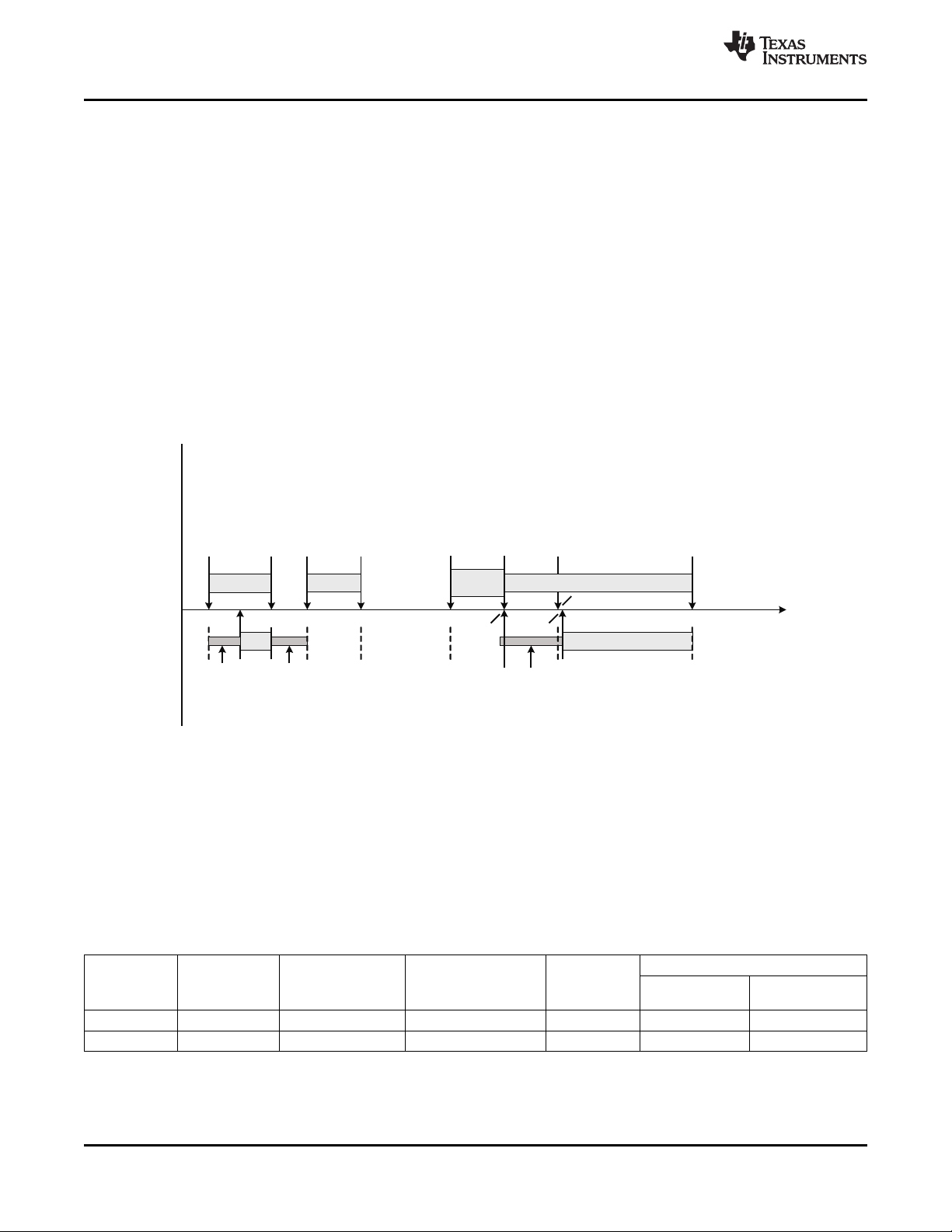
Figure 2. GATE and GAT2 Timing and Phasing
DEVICE INFORMATION
FUNCTIONAL BLOCK DIAGRAM
www.ti.com
Product Folder Link(s): TPS23754 TPS23754-1 TPS23756
6 Submit Documentation Feedback Copyright © 2008 – 2009, Texas Instruments Incorporated
PAD=V
SS
N/C=LeavePinUnused
TPS23754-1
1
2
3
4
5
6
7
15
14
13
11
12
8
16
V
DD
DEN
DT
FRS
CLS
GATE
RTN
V
C
CS
V
SS
V
B
CTL
T2P
BLNK
GAT2
10
9
19
18
17
20
PAD=V
SS
APD
ARTN
COM
TPS23754/6
PPD
V
DD1
1
2
3
4
5
6
7
15
14
13
11
12
8
16
V
DD
DEN
DT
FRS
CLS
GATE
RTN
V
C
CS
V
SS
V
B
CTL
T2P
BLNK
GAT2
10
9
19
18
17
20
APD
ARTN
COM
N/C
V
DD1
TPS23754
TPS23754-1
TPS23756
www.ti.com
NAME TYPE DESCRIPTION
CTL 1 1 I The control loop input to the PWM (pulse width modulator), typically driven by output regulation
V
B
CS 3 3 I/O DC/DC converter switching MOSFET current sense input. See R
COM 4 4 Gate driver return, connect to ARTN and RTN.
GATE 5 5 O Gate drive output for the main dc/dc converter switching MOSFET.
V
C
GAT2 7 7 O Gate drive output for a second dc/dc converter switching MOSFET (see Figure 1 ).
ARTN 8 8 ARTN is the dc/dc converter analog return. Tie to RTN and COM on the circuit board.
RTN 9 9 RTN is the output of the PoE hotswap MOSFET.
V
SS
V
DD1
V
DD
DEN 13 13 I/O Connect a 24.9 k Ω resistor from DEN to V
NC – 14 Float this no-connect pin.
PPD 14 – I Raising V
CLS 15 15 I Connect a resistor from CLS to V
DT 16 16 I Connect a resistor from DT to ARTN to set the GATE to GAT2 dead time. Tie DT to VBto disable
APD 17 17 I Raising V
BLNK 18 18 I Connect to ARTN to utilize the internally set current-sense blanking period, or connect a resistor from
FRS 19 19 I Connect a resistor from FRS to ARTN to program the converter switching frequency. FRS may be
T2P 20 20 O Active low output that indicates a PSE has performed the IEEE 802.3at type 2 hardware
Pad – – Connect to VSS.
Copyright © 2008 – 2009, Texas Instruments Incorporated Submit Documentation Feedback 7
....................................................................................................................................................... SLVS885B – OCTOBER 2008 – REVISED MAY 2009
(TOP VIEW)
PIN FUNCTIONS
NO.
' 754/6 ‘ 754-1
feedback (e.g. optocoupler). Use VBas a pullup for CTL.
2 2 O 5.1 V bias rail for dc/dc control circuits and the feedback optocoupler. Typically bypass with a 0.1 µ F
6 6 I/O DC/DC converter bias voltage. Connect a 0.47 µ F (minimum) ceramic capacitor to ARTN at the pin,
10 10 Connect to the negative power rail derived from the PoE source.
11 11 I Source of dc/dc converter startup current. Connect to V
12 12 I Connect to the positive PoE input power rail. V
to ARTN.
and a larger capacitor to power startup.
for many applications.
DD
powers the PoE interface circuits. Bypass with a
0.1 µ F capacitor and protect with a TVS.
to V
during powered operation causes the internal hotswap MOSFET to turn off.
SS
above 1.55 V enables the hotswap MOSFET and activates T2P. Connecting PPD
to V
resistor during classification to set class current.
GAT2 operation.
active. This forces power to come from a external V
used.
BLNK to ARTN to program a more accurate period.
used to synchronize the converter to an external timing source.
classification, PPD is active, or APD is active.
PPD-VSS
enables classification when APD is active. Tie PPD to V
DD
to program classification current. 2.5 V is applied to the program
SS
-V
APD
above 1.5 V disables the internal hotswap switch, turns class off, and forces T2P
ARTN
Product Folder Link(s): TPS23754 TPS23754-1 TPS23756
DD
to provide the PoE detection signature. Pulling this pin
DD
DD1-RTN
in Figure 1 .
CS
or float when not used.
SS
adapter. Tie APD to ARTN when not

( )
( )
APD1 APD2 ADPTR_ON APDEN APDEN
APD1 APD2
ADPTR_OFF APDEN APDH
APD2
R = R V V V
R + R
V = V V
R
´ -
´ -
( ) ( )
BLNK BLNK
R k = t nsW
TPS23754
TPS23754-1
TPS23756
SLVS885B – OCTOBER 2008 – REVISED MAY 2009 .......................................................................................................................................................
PIN DESCRIPTION
Refer to Figure 1 for component reference designators (R
for values denoted by reference (V
for example). Electrical Characteristic values take precedence over any
CSMAX
numerical values used in the following sections.
APD
APD forces power to come from an external adapter connected from V
switch, disabling the CLS output (see PPD pin description), and enabling the T2P output. A resistor divider is
recommended on APD when it is connected to an external adapter. The divider provides ESD protection,
leakage discharge for the adapter ORing diode, and input voltage qualification. Voltage qualification assures the
adapter output voltage is high enough that it can support the PD before the PoE current is cut off.
Select the APD divider resistors per Equation 1 where V
APD function as adapter voltage rises.
Place the APD pull-down resistor adjacent to the APD pin.
APD should be tied to ARTN when not used.
for example), and the Electrical Characteristics table
CS
to RTN by opening the hotswap
DD1
ADPTR-ON
is the desired adapter voltage that enables the
www.ti.com
(1)
BLNK
Blanking provides an interval between GATE going high and the current-control comparators on CS actively
monitoring the input. This delay allows the normal turn-on current transient (spike) to subside before the
comparators are active, preventing undesired short duty cycles and premature current limiting.
Connect BLNK to ARTN to obtain the internally set blanking period. Connect a resistor from BLNK to ARTN for a
more accurate, programmable blanking period. The relationship between the desired blanking period and the
programming resistor is defined by Equation 2 .
Place the resistor adjacent to the BLNK pin when it is used.
CLS
A resistor from CLS to V
programs the classification current per the IEEE standard. The PD power ranges and
SS
corresponding resistor values are listed in Table 1 . The power assigned should correspond to the maximum
average power drawn by the PD during operation.
High-power PSEs may perform two classification cycles if Class 4 is presented on the first cycle. The TPS23754
presents the same (resistor programmed) class each cycle per the standard.
Table 1. Class Resistor Selection
POWER AT PD
CLASS NOTES
MINIMUM MAXIMUM
(W) (W)
0 0.44 12.95 1270 Minimum may be reduced by pulsed loading. Serves as a catch-all default class.
1 0.44 3.84 243
2 3.84 6.49 137
3 6.49 12.95 90.9
4 12.95 25.5 63.4 Not allowed for IEEE 802.3-2005. Use to indicate a Type 2 PD (high power) per
RESISTOR
( Ω )
IEEE 802.3at.
(2)
8 Submit Documentation Feedback Copyright © 2008 – 2009, Texas Instruments Incorporated
Product Folder Link(s): TPS23754 TPS23754-1 TPS23756

( )
( )
DT
DT
t ns
R k =
2
W
FRS
SW
17250
R (k ) =
f (kHz)
W
TPS23754-1
www.ti.com
CS
The CS (current sense) input for the dc/dc converter should be connected to the high side of the switching
MOSFET ’ s current sense resistor (R
which the GATE ON time will be terminated regardless of the voltage on CTL.
The TPS23754 provides internal slope compensation (150 mV, V
compensation, a peak current limiter, and an off-time pull-down to this pin.
Routing between the current-sense resistor and the CS pin should be short to minimize cross-talk from noisy
traces such as the gate drive signal.
CTL
CTL (control) is the voltage-control loop input to the PWM (pulse width modulator). Pulling V
causes GATE to stop switching. Increasing V
MOSFET programmed peak current. The maximum (peak) current is requested at approximately V
V
CSMAX
approximately 100 k Ω .
Use V
DEN
DEN (detection and enable) is a multifunction pin for PoE detection and inhibiting operation from PoE power.
Connect a 24.9 k Ω resistor from DEN to V
high-impedance state when V
operation causes the internal hotswap MOSFET and class regulator to turn off, while the reduced detection
resistance prevents the PD from properly re-detecting.
....................................................................................................................................................... SLVS885B – OCTOBER 2008 – REVISED MAY 2009
). The current-limit threshold, V
CS
above V
CTL
ZDC
SLOPE
(zero duty cycle voltage) raises the switching
, defines the voltage on CS above
CSMAX
), an output current for additional slope
CTL
). The ac gain from CTL to the PWM comparator is 0.5. The internal divider from CTL to ARTN is
as a pull up source for CTL.
B
to provide the PoE detection signature. DEN goes to a
VDD-VSS
is outside of the detection range. Pulling DEN to V
DD
during powered
SS
TPS23754
TPS23756
below V
ZDC
ZDC
+ (2 ×
DT
Dead-time programming sets the delay between GATE and GAT2 to prevent overlap of MOSFET ON times as
shown in Figure 2 . GAT2 turns the second MOSFET off when it transitions high. Both MOSFETs should be off
between GAT2 going high to GATE going high, and GATE going low to GAT2 going low. The maximum GATE
ON time is reduced by the programmed dead-time period. The dead time period is specified with 1 nF of
capacitance on GATE and GAT2. Different loading on these pins will change the effective dead time.
A resistor connected from DT to ARTN sets the delay between GATE and GAT2 per Equation 3 .
Connect DT to V
to set the dead time to 0 and turn GAT2 off.
B
FRS
Connect a resistor from FRS (frequency and synchronization) to ARTN to program the converter switching
frequency. Select the resistor per the following relationship.
The converter may be synchronized to a frequency above its maximum free-running frequency by applying short
ac-coupled pulses into the FRS pin per Figure 30 .
The FRS pin is high impedance. Keep the connections short and apart from potential noise sources. Special care
should be taken to avoid crosstalk when synchronizing circuits are used.
(3)
(4)
GATE
Gate drive output for the dc/dc converter ’ s main switching MOSFET. GATE ’ s phase turns the main switch on
when it transitions high, and off when it transitions low. GATE is held low when the converter is disabled.
Copyright © 2008 – 2009, Texas Instruments Incorporated Submit Documentation Feedback 9
Product Folder Link(s): TPS23754 TPS23754-1 TPS23756

( )
( )
ADPTR_ON PPDEN
PPD 1
PPD EN
PPD
PPD2
PP DEN PPDH
ADP TR_OFF PPDEN PPD H P PD1 PP D
PPD2
V V
R =
V
I
R
V V
V = V V + R I
R
æ ö
ç ÷
-
ç ÷
ç ÷
-
ç ÷
è ø
é ù
æ ö
-
ê ú- ´ -ç ÷
ç ÷
ê ú
è ø
ë û
TPS23754
TPS23754-1
TPS23756
SLVS885B – OCTOBER 2008 – REVISED MAY 2009 .......................................................................................................................................................
GAT2
GAT2 is the second gate drive output for the dc/dc converter. GAT2 ’ s phase turns the second switch off when it
transitions high, and on when it transitions low. This drives active-clamp PMOS devices per Figure 1 , and driven
flyback synchronous rectifiers per Figure 28 . See the DT Pin Description for GATE to GAT2 timing. Connecting
DT to V
disables GAT2 in a high-impedance condition. GAT2 is low when the converter is disabled.
B
PPD
PPD is a multifunction pin that has two voltage thresholds, PPD1 and PPD2.
PPD1 permits power to come from an external low voltage adapter, e.g., 24 V, connected from V
over-riding the normal hotswap UVLO. Voltage on PPD above 1.55 V (V
) enables the hotswap MOSFET,
PPDEN
inhibits class current, and enables T2P. A resistor divider per Figure 35 provides ESD protection, leakage
discharge for the adapter ORing diode, reverse adapter protection, and input voltage qualification. Voltage
qualification assures the adapter output voltage is high enough that it can support the PD before it begins to draw
current.
www.ti.com
to V
DD
SS
by
PPD2 enables normal class regulator operation when V
APD is used in conjunction with diode D
(see Figure 34 ). Tie PPD to V
VDD
is above 8.3 V to permit type 2 classification when
PPD
when PPD2 operation is desired.
DD
The PPD pin has a 5 µ A internal pull-down current.
Locate the PPD pull-down resistor adjacent to the pin when used.
PPD may be tied to V
or left open when not used.
SS
RTN, ARTN, COM
RTN is internally connected to the drain of the PoE hotswap MOSFET, while ARTN is the quiet analog reference
for the dc/dc controller return. COM serves as the return path for the gate drivers and should be tied to ARTN on
the circuit board. The ARTN / COM / RTN net should be treated as a local reference plane (ground plane) for the
dc/dc control and converter primary. RTN and (ARTN/COM) may be separated by several volts for special
applications.
T2P
T2P is an active low output that indicates [ (V
classification observed) ]. T2P is valid after both a delay of t
(V
– 1 V)]. Once T2P is valid, V
B
will not effect it. T2P will become invalid if the converter goes back into
CTL
softstart, over-temperature, or is held off by the PD during C
> 1.5 V) OR (1.55 V ≤ V
APD
from the start of converter switching, and [V
T2P
recharge (inrush). T2P is referenced to ARTN and
IN
≤ 8.3 V) OR (type 2 hardware
PPD
is intended to drive the diode side of an optocoupler. T2P should be left open or tied to ARTN if not used.
V
B
V
is an internal 5.1V regulated dc/dc controller supply rail that is typically bypassed by a 0.1 µ F capacitor to
B
ARTN. V
should be used to bias the feedback optocoupler.
B
(5)
≤
CTL
V
C
V
is the bias supply for the dc/dc controller. The MOSFET gate drivers run directly from VC. V
C
down from VC, and is the bias voltage for the rest of the converter control. A startup current source from V
V
is controlled by a comparator with hysteresis to implement the converter bootstrap startup. V
C
connected to a bias source, such as a converter auxiliary output, during normal operation.
10 Submit Documentation Feedback Copyright © 2008 – 2009, Texas Instruments Incorporated
Product Folder Link(s): TPS23754 TPS23754-1 TPS23756
is regulated
B
C
must be
to
DD1
(V
VDD
− V
VSS
) − PoE Voltage − V
0
1
2
3
4
5
6
7
8
0 2 4 6 8 10
I
VDD
− Bias Current − µA
G001
−40°C
25°C
125°C
TJ − Junction Temperature − °C
910
920
930
940
950
960
970
−40 −20 0 20 40 60 80 100 120
PoE − Current Limit − mA
G002
Pulsed Current Measurement
TPS23754
TPS23754-1
TPS23756
www.ti.com
....................................................................................................................................................... SLVS885B – OCTOBER 2008 – REVISED MAY 2009
A minimum 0.47 µ F capacitor, located adjacent to the V
pin, should be connected from V
C
C
to COM to bypass
the gate driver. A larger total capacitance is required for startup to provide control power between the time the
converter starts switching and the availability of the converter auxiliary output voltage.
V
DD
V
is the positive input power rail that is derived from the PoE source (PSE). V
DD
should be bypassed to V
DD
with a 0.1 µ F capacitor as required by the IEEE standard. A transient suppressor diode (TVS), a special type of
Zener diode, such as SMAJ58A should be connected from V
V
DD1
V
is the dc/dc converter startup supply. Connect to V
DD1
diode from V
V
SS
V
is the PoE input-power return side. It is the reference for the PoE interface circuits, and has a current-limited
SS
hotswap switch that connects it to RTN. V
A local V
to support PoE priority operation.
DD
is clamped to a diode drop above RTN by the hotswap switch.
SS
reference plane should be used to connect the input bypass capacitor, TVS, R
SS
to V
DD
for many applications. V
DD
to protect against over-voltage transients.
SS
may be isolated by a
DD1
CLS
, and the
PowerPad. This plane becomes the main heatsink for the TPS23754.
V
is internally connected to the PowerPAD.
SS
PowerPAD
The Powerpad is internally connected to V
. It should be tied to a large V
SS
copper area on the PCB to provide
SS
a low resistance thermal path to the circuit board. It is recommended that a clearance of 0.025 ” be maintained
between V
, RTN, and various control signals to high-voltage signals such as V
SS
and V
DD
.
DD1
SS
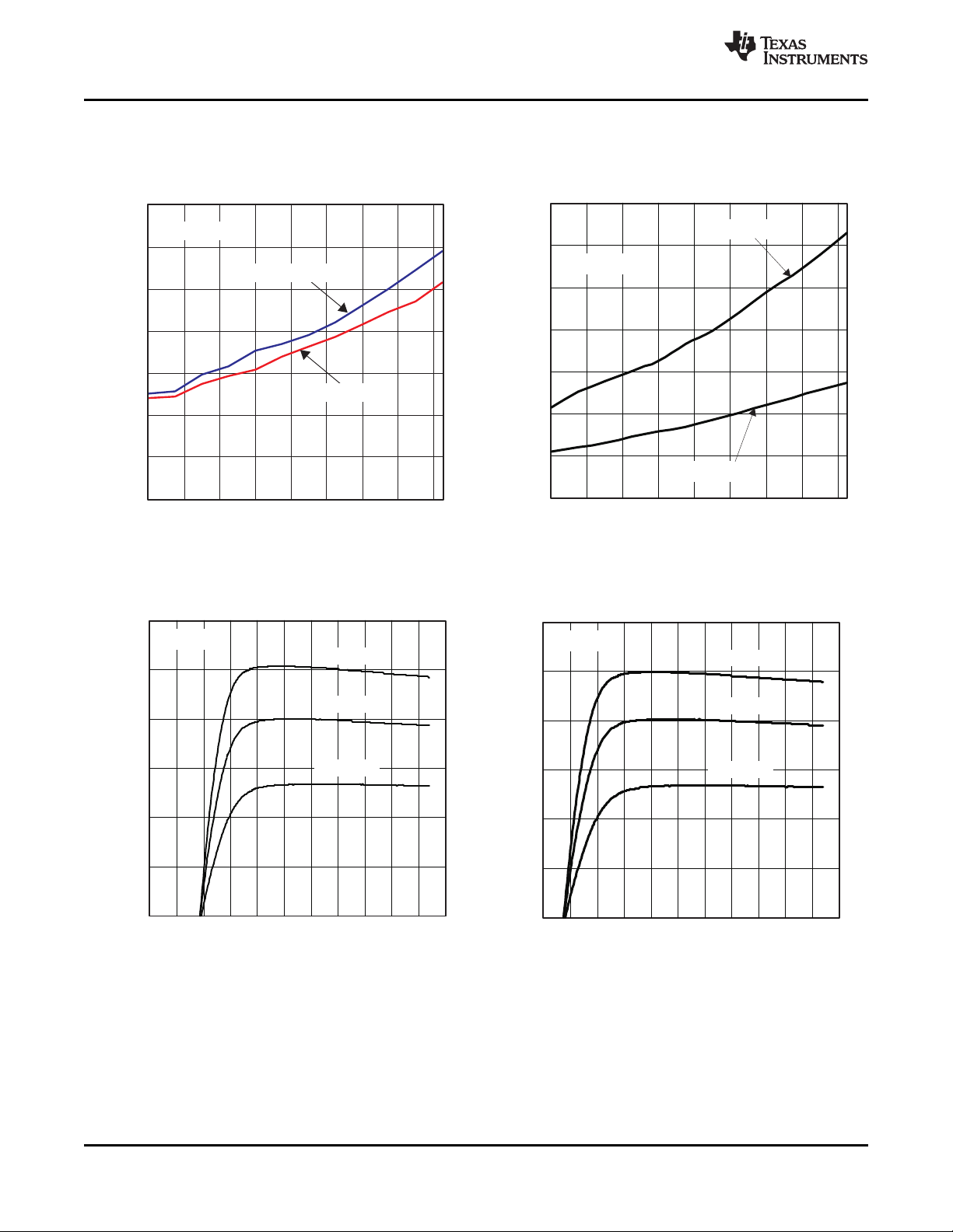
DETECTION BIAS CURRENT PoE CURRENT LIMIT
VOLTAGE TEMPERATURE
Copyright © 2008 – 2009, Texas Instruments Incorporated Submit Documentation Feedback 11
TYPICAL CHARACTERISTICS
vs vs
Figure 3. Figure 4.
Product Folder Link(s): TPS23754 TPS23754-1 TPS23756
−40 −20 0 20 40 60 80 100 120
TJ-Junction Temperature- C
o
20
100
140
160
Start Time − ms
CVC=22 Fm
V
VDD1
=10.2V
V
VDD1
=35V
120
80
60
40
TJ − Junction Temperature − °C
20
40
60
80
100
120
140
160
−40 −20 0 20 40 60 80 100 120
Converter Start Time − ms
G003
CVC = 22 µF
V
VDD1
= 35 V
V
VDD1
= 19.2 V
5 10 15 25 30 35 40 50 60
V − V
VDD1-RTN
0
1
2
6
I SourceCurrent − mA
VC
−
5520 45
3
4
5
T =-40 C
J
o
V =13.9
VC
V
T =25 C
J
o
T =125 C
J
o
5 10 15 25 30 35 40 50 60
V − V
VDD1-RTN
0
1
2
6
I SourceCurrent −
mA
VC
−
5520 45
3
4
5
T =-40 C
J
o
V =
VC
8.6V
T =25 C
J
o
T =125 C
J
o
TPS23754
TPS23754-1
TPS23756
SLVS885B – OCTOBER 2008 – REVISED MAY 2009 .......................................................................................................................................................
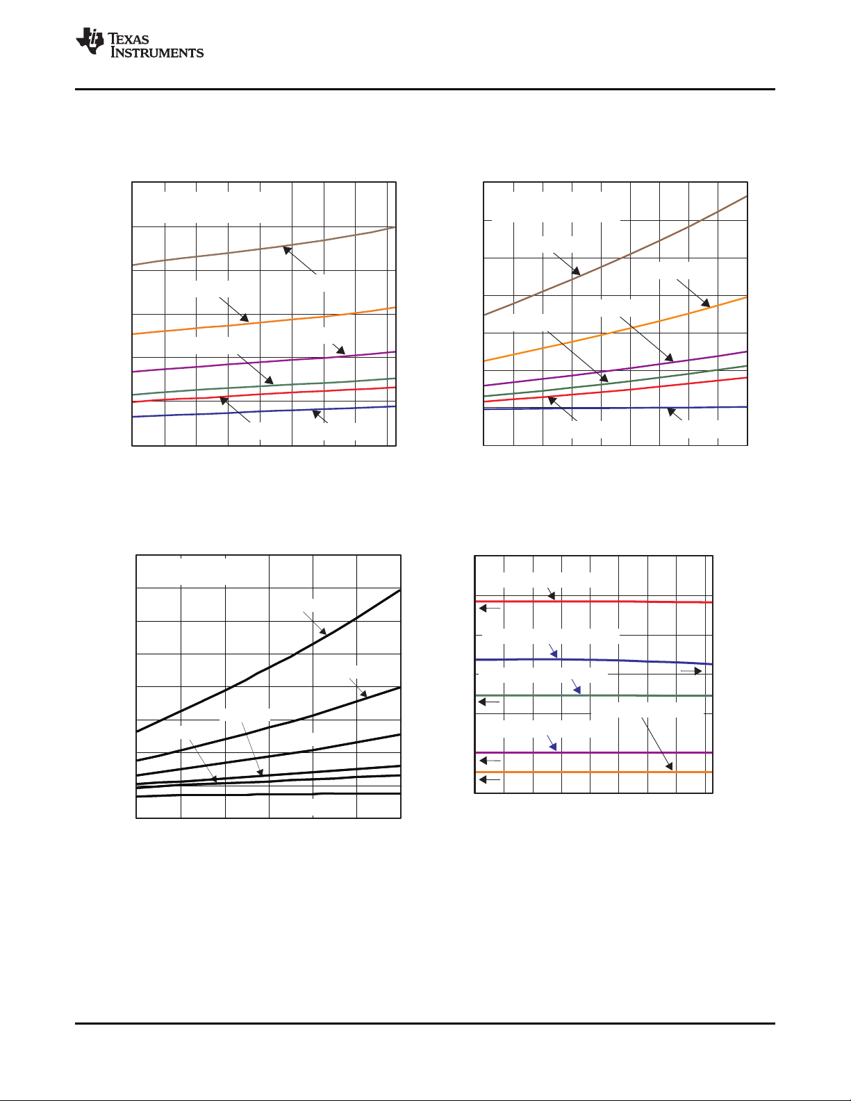
TYPICAL CHARACTERISTICS (continued)
www.ti.com
' 754 CONVERTER START TIME ' 756 CONVERTER START TIME
vs vs
TEMPERATURE TEMPERATURE
Figure 5. Figure 6.
' 754 CONVERTER STARTUP CURRENT ' 756 CONVERTER STARTUP CURRENT
vs vs
V
VDD1
V
VDD1
12 Submit Documentation Feedback Copyright © 2008 – 2009, Texas Instruments Incorporated
Figure 7. Figure 8.
Product Folder Link(s): TPS23754 TPS23754-1 TPS23756
TJ-Junction Temperature- °C
0
500
1000
1500
2000
2500
3000
−40 −20 0 20 40 60 80 100 120
I
VC
−
Sinking −
mA
G005
VVC=12V
GATEandGAT2Open
937kHz
484kHz
100kHz
50kHz
V
CTL
=0V
245kHz
VC− ControllerBiasV
oltage − V
0
500
1000
1500
2000
2500
3000
3500
9 10 11 12 13 14 15 16 17 18
I
C
− ControllerBiasCurrent −
mA
G006
TJ=25°C
GATEandGAT2Open
484kHz
50kHz
V
CTL
=0V
937kHz
245kHz
100kHz
−40 −20 0 20 40 60 80 100 120
TJ-Junction Temperature- °C
0
100
200
300
400
500
600
SwitchingFrequency −
kHz
G007
SwitchingFrequency
−
kHz
900
800
700
600
1000
1100
1200
R
FRS
=69.8kΩ (245kHz)
R
FRS
=173kΩ (100kHz)
R
FRS
=347kΩ (50kHz)
R
FRS
=34.6kΩ (484kHz)
R
FRS
=17.35kΩ (937kHz)
6 8 10 12 14 18
V − ControllerBiasVoltage − V
C
0
1500
V BiasCurrent − A
C
m−
16
500
4000
1000
2000
2500
3000
3500
GATE,GAT2open
T =25 C
J
o
960kHz
480kHz
250kHz
100kHz
50kHz
V =0V
CTL
TPS23754
TPS23754-1
TPS23756
www.ti.com
....................................................................................................................................................... SLVS885B – OCTOBER 2008 – REVISED MAY 2009
TYPICAL CHARACTERISTICS (continued)
CONTROLLER BIAS CURRENT ' 754 CONTROLLER BIAS CURRENT
vs vs
TEMPERATURE VOLTAGE
Figure 9. Figure 10.
' 756 CONTROLLER BIAS CURRENT SWITCHING FREQUENCY
vs vs
VOLTAGE TEMPERATURE
Copyright © 2008 – 2009, Texas Instruments Incorporated Submit Documentation Feedback 13
Figure 11. Figure 12.
Product Folder Link(s): TPS23754 TPS23754-1 TPS23756

TJ-Junction Temperature- °C
70
71
72
73
74
75
76
77
78
79
−40 −20 0 20 40 60 80 100 120
MaximumDutyCycle − %
G009
R
FRS
=17.3k (937kHz)W
R
FRS
=34.6k (484kHz)W
R
FRS
=69.8k (245kHz)W
R
FRS
=21.5k (766kHz)W
R
FRS
=347k (50kHz)W
R
FRS
=26.7k (623kHz)W
Programmed Resistance (106 / R
FRS
) − Ω
−1
0
200
400
600
800
1000
1200
0 10 20 30 40 50 60
Switching Frequency − kHz
G008
Ideal
Typical
TJ − Junction Temperature − °C
30
35
40
45
50
−40 −20 0 20 40 60 80 100 120
I
SLOPE
− µA
PP
G011
TJ − Junction Temperature − °C
149
150
151
152
153
154
155
−40 −20 0 20 40 60 80 100 120
V
SLOPE
− mV
PP
G010
TPS23754
TPS23754-1
TPS23756
SLVS885B – OCTOBER 2008 – REVISED MAY 2009 .......................................................................................................................................................
TYPICAL CHARACTERISTICS (continued)
www.ti.com
SWITCHING FREQUENCY MAXIMUM DUTY CYCLE
vs vs
PROGRAM CONDUCTANCE TEMPERATURE
Figure 13. Figure 14.
CURRENT SLOPE COMPENSATION VOLTAGE CURRENT SLOPE COMPENSATION CURRENT
vs vs
TEMPERATURE TEMPERATURE
14 Submit Documentation Feedback Copyright © 2008 – 2009, Texas Instruments Incorporated
Figure 15. Figure 16.
Product Folder Link(s): TPS23754 TPS23754-1 TPS23756

−40 −20 0 20 40 60 80 100 120
TJ-Junction Temperature- °C
45
55
65
75
85
95
105
115
BlankingPeriod
− ns
G012
BlankingPeriod
−
ns
R
BLNK
=249kΩ
245
240
235
230
250
255
265
260
R
BLNK
=49.9kΩ
R
BLNK
=RTN
R
BLNK
=100kΩ
0 50 100 150 200 250 300 350 400
R
BLNK
− kΩ
BlankingPeriod
−
ns
G013
Dif
ferenceFromComputed
−
ns
−6
−10
−14
−18
−2
2
18
6
10
14
150
100
50
0
200
250
450
300
350
400
0
100
200
300
400
500
600
700
800
900
0 50 100 150 200 250 300 350
Dead TimeResistance-kW
Dead
T
ime-ns
Ideal
Typical
400
6
7
8
9
10
11
-40 -20 0 20 40 60 80 100 120
Temperature- C°
T2P
Delay Time-ms
TPS23754
TPS23754-1
TPS23756
www.ti.com
....................................................................................................................................................... SLVS885B – OCTOBER 2008 – REVISED MAY 2009
TYPICAL CHARACTERISTICS (continued)
BLANKING PERIOD BLANKING PERIOD
vs vs
TEMPERATURE Blanking Resistance (R
Figure 17. Figure 18.
DEAD TIME T2P DELAY TIME
vs vs
DEAD TIME RESISTANCE (R
) TEMPERATURE
DT
)
BLNK
PoE OVERVIEW
The following text is intended as an aid in understanding the operation of the TPS23754 but not as a substitute
for the actual IEEE 802.3-2005 or IEEE 802.3at standard. The pending IEEE 802.3at standard is an update to
IEEE 802.3-2005 clause 33 (PoE), adding high-power options and enhanced classification. Generally speaking, a
device compliant to IEEE 802.3-2005 will be referred to as a type 1 device, and devices with high power and
enhanced classification will be referred to as type 2 devices. Standards change and should always be referenced
when making design decisions.
Copyright © 2008 – 2009, Texas Instruments Incorporated Submit Documentation Feedback 15
Figure 19. Figure 20.
DETAILED DESCRIPTION
Product Folder Link(s): TPS23754 TPS23754-1 TPS23756
57
4237
3020.514.510.12.7
D
etecti
on
Lo
wer L
imit
Detection
Upper Limit
C
l
a
s
s
i
f
i
c
a
t
i
o
n
L
o
w
e
r
L
i
m
i
t
Classification
Upper Limit
Mus
t Turn
Off by
-
Volta
ge Fal
ling
Lower Limit -
Operating Range
M
u
s
t
T
u
r
n
O
n
b
y
-
V
o
l
t
a
g
e
R
i
s
i
n
g
M
a
xi
mu
m
I
np
ut
V
ol
ta
ge
Detect
Classify
Shutdown
PIVoltage(V)
0
Lower Limit -
13W Op.
Mark
Class-Mark
Transition
250m s
Transient
6.9
NormalOperation
IEE
E 802
.3-200
5
IEEE
802.3
at
NormalOperation
T2 Reset
Range
42.5
TPS23754
TPS23754-1
TPS23756
SLVS885B – OCTOBER 2008 – REVISED MAY 2009 .......................................................................................................................................................
The IEEE 802.3-2005 (802.3at) standard defines a method of safely powering a PD (powered device) over a
cable by power sourcing equipment (PSE), and then removing power if a PD is disconnected. The process
proceeds through an idle state and three operational states of detection, classification, and operation. The PSE
leaves the cable unpowered (idle state) while it periodically looks to see if something has been plugged in; this is
referred to as detection. The low power levels used during detection are unlikely to damage devices not designed
for PoE. If a valid PD signature is present, the PSE my inquire how much power the PD requires; this is referred
to as classification. The PSE may then power the PD if it has adequate capacity.
Type 2 PSEs are required to do type 1 hardware classification plus a (new) data-layer classification, or an
enhanced type 2 hardware classification. Type 1 PSEs are not required to do hardware or data link layer (DLL)
classification. A type 2 PD must do type 2 hardware classification as well as DLL classification. The PD may
return the default 12.95W (often referred to as 13W) current-encoded class, or one of four other choices. DLL
classification occurs after power-on and the ethernet data link has been established.
Once started, the PD must present the maintain power signature (MPS) to assure the PSE that it is still present.
The PSE monitors its output for a valid MPS, and turns the port off if it loses the MPS. Loss of the MPS returns
the PSE to the idle state. Figure 21 shows the operational states as a function of PD input voltage. The upper
half is for IEEE 802.3-2005, and the lower half shows specific differences for IEEE 802.3at. The dashed lines in
the lower half indicate these are the same (e.g., Detect and Class) for both.
www.ti.com
Figure 21. Operational States for PD
The PD input, typically an RJ-45 eight-lead connector, is referred to as the power interface (PI). PD input
requirements differ from PSE output requirements to account for voltage drops and operating margin. The
standard allots the maximum loss to the cable regardless of the actual installation to simplify implementation.
IEEE 802.3-2005 was designed to run over infrastructure including ISO/IEC 11801 class C (CAT3 per
TIA/EIA-568) that may have had AWG 26 conductors. IEEE 802.3at cabling power loss allotments and voltage
drops have been adjusted for 12.5 Ω power loops per ISO/IEC11801 class D (CAT5 or higher per TIA/EIA-568,
typically AWG #24 conductors). Table 2 shows key operational limits broken out for the two revisions of the
standard.
Table 2. Comparison of Operational Limits
POWER LOOP PSE PSE STATIC PD INPUT STATIC PD INPUT VOLTAGE
STANDARD
'2005 20 Ω 15.4 W 44 V 12.95 W 37 V – 57 V N/A
802.3at 12.5 Ω 36 W 50 V 25.5 W 37 V – 57 V 42.5 V – 57 V
16 Submit Documentation Feedback Copyright © 2008 – 2009, Texas Instruments Incorporated
RESISTANCE
(max)
OUTPUT POWER OUTPUT VOLTAGE POWER
(min) (min) (max)
Product Folder Link(s): TPS23754 TPS23754-1 TPS23756
POWER ≤ POWER >
12.95 W 12.95 W

V
UVLO_R
Detection
Classification
PDPowered
Idle
V
CL_ON
V
CL_H
V
CU_OFF
V
CU_H
Note:VariablenamesrefertoElectricalCharacteristic
Tableparameters
VDD-V
SS
V
UVLO_H
Mark
V
MSR
Functional
State
TPS23754
TPS23754-1
TPS23756
www.ti.com
The PSE can apply voltage either between the RX and TX pairs (pins 1 - 2 and 3 - 6 for 10baseT or 100baseT),
or between the two spare pairs (4 - 5 and 7 - 8). Power application to the same pin combinations in 1000baseT
systems is recognized in 802.3at. 1000baseT systems can handle data on all pairs, eliminating the spare pair
terminology. The PSE may only apply voltage to one set of pairs at a time. The PD uses input diode bridges to
accept power from any of the possible PSE configurations. The voltage drops associated with the input bridges
create a difference between the standard limits at the PI and the TPS23754 specifications.
A compliant type 2 PD has power management requirements not present with a type 1 PD. These requirements
include the following:
1. Must interpret type 2 hardware classification
2. Must present hardware class 4
3. Must implement DLL negotiation
4. Must behave like a type 1 PD during inrush and startup
5. Must not draw more than 13W for 80ms after PSE applies operating voltage (power-up)
6. Must not draw more than 13W if it has not received a type 2 hardware classification or received permission
7. Must meet various operating and transient templates
8. Optionally monitor for the presence or absence of an adapter (assume high power).
As a result of these requirements, the PD must be able to dynamically control its loading, and monitor T2P for
changes. In cases where the design needs to know specifically if an adapter is plugged in and operational, the
adapter should be individually monitored, typically with an optocoupler.
....................................................................................................................................................... SLVS885B – OCTOBER 2008 – REVISED MAY 2009
through DLL
Threshold Voltages
The TPS23754 has a number of internal comparators with hysteresis for stable switching between the various
states. Figure 22 relates the parameters in the Electrical Characteristics section to the PoE states. The mode
labeled idle between classification and operation implies that the DEN, CLS, and RTN pins are all high
impedance. The state labeled Mark, which is drawn in dashed lines, is part of the new type 2 hardware class
state machine.
Figure 22. Threshold Voltages
PoE Startup Sequence
The waveforms of Figure 23 demonstrate detection, classification, and startup from a PSE with type 2 hardware
classification. The key waveforms shown are V
two detection levels, two class and mark cycles, and startup from the second mark event. V
TPS23754 charges C
current as seen in the IPIwaveform.
Copyright © 2008 – 2009, Texas Instruments Incorporated Submit Documentation Feedback 17
following application of full voltage. Subsequently, the converter starts up, drawing
IN
Product Folder Link(s): TPS23754 TPS23754-1 TPS23756
-V
VDD
, V
-V
VSS
RTN
, and IPI. IEEE 802.3at requires a minimum of
VSS
to V
RTN
SS
falls as the

t-Time-25ms/div
50mA/div
10mA/div
I
PI
Inrush
V
VDD-VSS
Cvtr.Starts
V
RTN-VSS
Mark
Class
Detect
TPS23754
TPS23754-1
TPS23756
SLVS885B – OCTOBER 2008 – REVISED MAY 2009 .......................................................................................................................................................
Figure 23. Startup
www.ti.com
Detection
The TPS23754 drives DEN to V
input voltage rises above V
CL-ON
detection, RTN is high impedance, and almost all the internal circuits are disabled. An R
whenever V
SS
-V
VDD
is below the lower classification threshold. When the
VSS
, the DEN pin goes to an open-drain condition to conserve power. While in
of 24.9 k Ω (1%),
DEN
presents the correct signature. It may be a small, low-power resistor since it only sees a stress of about 5 mW. A
valid PD detection signature is an incremental resistance ( Δ V / Δ I ) between 23.75 k Ω and 26.25 k Ω at the PI.
The detection resistance seen by the PSE at the PI is the result of the input bridge resistance in series with the
parallel combination of R
and internal V
DEN
loading. The input diode bridge ’ s incremental resistance may be
DD
hundreds of ohms at the very low currents drawn when 2.7 V is applied to the PI. The input bridge resistance is
partially cancelled by the TPS23754's effective resistance during detection.
The type 2 hardware classification protocol of IEEE 802.3at specifies that a type 2 PSE drops its output voltage
into the detection range during the classification sequence. The PD is required to have an incorrect detection
signature in this condition, which is referred to as the mark event (see Figure 23 ). After the first mark event, the
TPS23754 will present a signature less than 12 k Ω until it has experienced a V
reset (V
). This is explained more fully under Hardware Classification.
MSR
-V
VDD
voltage below the mark
VSS
Hardware Classification
Hardware classification allows a PSE to determine a PD ’ s power requirements before powering, and helps with
power management once power is applied. Type 2 hardware classification permits high power PSEs and PDs to
determine whether the connected device can support high-power operation. A type 2 PD presents class 4 in
hardware to indicate it is a high-power device. A type 1 PSE will treat a class 4 device like a class 0 device,
allotting 12.95 W if it chooses to power the PD. A PD that receives a 2 event class understands that it is powered
from a high-power PSE and it may draw up to 25.5 W immediately after the 80 ms startup period completes. A
type 2 PD that does not receive a 2-event hardware classification may choose to not start, or must start in a 13
W condition and request more power through the DLL after startup. The standard requires a type 2 PD to
indicate that it is underpowered if this occurs. Startup of a high-power PD under 13 W implicitly requires some
form of powering down sections of the application circuits.
The maximum power entries in Table 1 determine the class the PD must advertise. The PSE may disconnect a
PD if it draws more than its stated Class power, which may be the hardware class or a lower DLL-derived power
level. The standard permits the PD to draw limited current peaks that increase the instantaneous power above
the Table 1 limit, however the average power requirement always applies.
18 Submit Documentation Feedback Copyright © 2008 – 2009, Texas Instruments Incorporated
Product Folder Link(s): TPS23754 TPS23754-1 TPS23756

Idle Detect Class
Mark Class
Mark Class
Between
Ranges
Between
Ranges
Operating
T2P
open-drain
Operating
T2P low
Mark
Reset
Between
Ranges
UVLO
Rising
UVLO
Falling
UVLO
Rising
UVLO
Falling
TYPE2PSE
HardwareClass
ClassMark
Mark
Reset
TYPE1PSE
HardwareClass
TPS23754
TPS23754-1
TPS23756
www.ti.com
....................................................................................................................................................... SLVS885B – OCTOBER 2008 – REVISED MAY 2009
The TPS23754 implements two-event classification. Selecting an R
of 63.4 Ω provides a valid type 2
CLS
signature. TPS23754 may be used as a compatible type 1 device simply by programming class 0 – 3 per Table 1 .
DLL communication is implemented by the ethernet communication system in the PD and is not implemented by
the TPS23754.
The TPS23754 disables classification above V
CU_OFF
to avoid excessive power dissipation. CLS voltage is turned
off during PD thermal limit or when APD or DEN are active. The CLS output is inherently current limited, but
should not be shorted to V
for long periods of time.
SS
Figure 24 shows how classification works for the TPS23754. Transition from state-to-state occurs when
comparator thresholds are crossed (see Figure 21 and Figure 22 ). These comparators have hysteresis, which
adds inherent memory to the machine. Operation begins at idle (unpowered by PSE) and proceeds with
increasing voltage from left to right. A 2-event classification follows the (heavy lined) path towards the bottom,
ending up with a latched type 2 decode along the lower branch that is highlighted. This state results in a low T2P
during normal operation. Once the valid path to type 2 PSE detection is broken, the input voltage must transition
below the mark reset threshold to start anew.
Inrush and Startup
802.3at has a startup current and time limitation, providing type 2 PSE compatibility for type 1 PDs. A type 2 PSE
limits output current to between 400 mA and 450 mA for up to 75 ms after power-up (applying “ 48 V ” to the PI) in
order to mirror type 1 PSE functionality. The type 2 PSE will support higher output current after 75 ms. The
TPS23754 implements a 140 mA inrush current, which is compatible with all PSE types. A high-power PD must
control its converter startup peak and operational currents drawn to below 400 mA for 80 ms. The TPS23754 ’ s
internal softstart permits control of the converter startup, however the application circuits must assure that their
power draw does not cause the PD to exceed the current/time limitation. This requirement implicitly requires
some form of powering down sections of the application circuits. T2P becomes valid within t
starts, or if an adapter is plugged in while the PD is operating from a PSE.
Maintain Power Signature
The MPS is an electrical signature presented by the PD to assure the PSE that it is still present after operating
voltage is applied. A valid MPS consists of a minimum dc current of 10 mA (or a 10 mA pulsed current for at
least 75 ms every 225 ms) and an ac impedance lower than 26.25 k Ω in parallel with 0.05 µ F. The ac impedance
is usually accomplished by the minimum operating C
force the hotswap switch off, the dc MPS will not be met. A PSE that monitors the dc MPS will remove power
from the PD when this occurs. A PSE that monitors only the ac MPS may remove power from the PD.
Copyright © 2008 – 2009, Texas Instruments Incorporated Submit Documentation Feedback 19
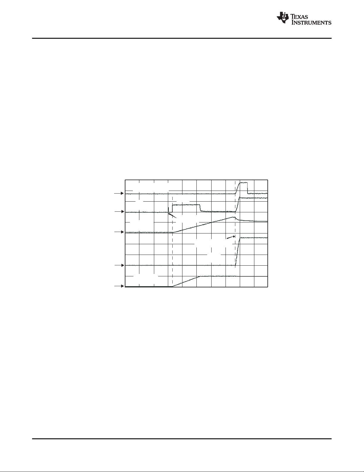
Figure 24. Two-Event Class Internal States
Product Folder Link(s): TPS23754 TPS23754-1 TPS23756
requirement of 5 µ F. When either APD or DEN is used to
IN
after switching
T2P
1
3
4
6
8
9
10
t-Time-10ms/div
I
PI
VDD-RTN
VC-RTN
Inrush
V
OUT
PIPowered
Switchingstarts
T2P @output
9
0
1
2
3
4
5
6
7
8
5V/div
200mA/div
10V/div
2V/div
50V/div
TPS23754
TPS23754-1
TPS23756
SLVS885B – OCTOBER 2008 – REVISED MAY 2009 .......................................................................................................................................................
Startup and Converter Operation
The internal PoE UVLO (Under Voltage Lock Out) circuit holds the hotswap switch off before the PSE provides
full voltage to the PD. This prevents the converter circuits from loading the PoE input during detection and
classification. The converter circuits will discharge C
, C
, and C
IN
VC
while the PD is unpowered. Thus V
VB
will be a small voltage just after full voltage is applied to the PD, as seen in Figure 23 . The PSE drives the PI
voltage to the operating range once it has decided to power up the PD. When V
turn-on threshold (V
, ~35 V) with RTN high, the TPS23754 enables the hotswap MOSFET with a ~140 mA
UVLO-R
(inrush) current limit as seen in Figure 25 . Converter switching is disabled while C
V
VDD
to nearly V
, however the converter startup circuit is allowed to charge C
VSS
IN
rises above the UVLO
VDD
charges and V
(the bootstrap startup
VC
capacitor). Converter switching is allowed if the PD is not in inrush, OTSD is not active, and the V
permits it. Once the inrush current falls about 10% below the inrush current limit, the PD current limit switches to
the operational level (~970 mA). Continuing the startup sequence shown in Figure 25 , V
the startup threshold (V
The V
regulator is always active, powering the internal converter circuits as V
B
, ~15 V or ~9 V) is exceeded, turning the startup source off and enabling switching.
CUV
VC
rises. There is a slight delay
continues to rise until
VC
between the removal of charge current and the start of switching as the softstart ramp sweeps above the V
threshold. V
control bias output rises to support V
occurs. T2P in Figure 23 (Figure 1 , V
falls as it powers both the internal circuits and the switching MOSFET gates. If the converter
VC
before it falls to V
VC
T2P-OUT
) becomes active within t
– V
CUV
(~8.5 V or ~5.5 V), a successful startup
CUVH
from the start of switching, indicating
T2P
that a type 2 PSE or an adapter is plugged in.
www.ti.com
VDD
falls from
RTN
UVLO
C
-V
RTN
ZDC
Figure 25. Power Up and Start
If V
- V
VDD
but the converter will still run. The converter will stop if V
or ~5.5 V), the hotswap is in inrush current limit, 0% duty cycle is demanded by V
drops below the lower PoE UVLO (V
VSS
UVLO-R
- V
falls below the converter UVLO (V
VC
, ~30.5 V), the hotswap MOSFET is turned off,
UVLO-H
(V
CTL
CTL
– V
CUV
< V
ZDC
the converter is in thermal shutdown.
PD Hotswap Operation
IEEE 802.3at has taken a new approach to PSE output limiting. A type 2 PSE must meet an output current vs.
time template with specified minimum and maximum sourcing boundaries. The peak output current may be as
high as 50 A for 10 µ s or 1.75 A for 75 ms. This makes robust protection of the PD device even more important
than it was in IEEE 802.3-2005.
The internal hotswap MOSFET is protected against output faults and input voltage steps with a current limit and
deglitched (time-delay filtered) foldback. An overload on the pass MOSFET engages the current limit, with
V
-V
RTN
inrush value, and turns the converter off. The 400 µ s deglitch feature prevents momentary transients from
20 Submit Documentation Feedback Copyright © 2008 – 2009, Texas Instruments Incorporated
rising as a result. If V
VSS
rises above ~12 V for longer than ~400 µ s, the current limit reverts to the
RTN
Product Folder Link(s): TPS23754 TPS23754-1 TPS23756
, ~8.5 V
CUVH
, ~1.5 V), or

t-Time-200 s/divm
I
PI
16VInputstep
V
RTN-VSS
V
VDD-VSS
CINcompletescharge
whileconverteroperates
RecoveryfromPIdropout
V
RTN
<12V@400 sm
20V/div
10V/div
500mA/div
TPS23754
TPS23754-1
TPS23756
www.ti.com
causing a PD reset, provided that recovery lies within the bounds of the hotswap and PSE protection. Figure 26
shows an example of recovery from a 16 V PSE rising voltage step. The hotswap MOSFET goes into current
limit, overshooting to a relatively low current, recovers to ~950 mA full current limit, and charges the input
capacitor while the converter continues to run. The MOSFET did not go into foldback because V
below 12 V after the 400 µ s deglitch.
....................................................................................................................................................... SLVS885B – OCTOBER 2008 – REVISED MAY 2009
-V
RTN
VSS
was
The PD control has a thermal sensor that protects the internal hotswap MOSFET. Conditions like startup or
operation into a V
(OTSD) turns off the hotswap MOSFET and class regulator, which are restarted after the device cools. The
hotswap MOSFET will be re-enabled with the inrush current limit when exiting from an over-temperature event.
Pulling DEN to V
allows a PD with Option three ORing per Figure 27 to achieve adapter priority. Care must be taken with
synchronous converter topologies that can deliver power in both directions.
The hotswap switch will be forced off under the following conditions:
Converter Controller Features
The TPS23754 dc/dc controller implements a typical current-mode control as shown in the Functional Block
Diagram. Features include oscillator, over-current and PWM comparators, current-sense blanker, dead-time
control, softstart, and gate driver. In addition, an internal slope-compensation ramp generator, frequency
synchronization logic, thermal shutdown, and startup current source with control are provided.
The TPS23754 is optimized for isolated converters, and does not provide an internal error amplifier. Instead, the
optocoupler feedback is directly fed to the CTL pin which serves as a current-demand control for the PWM.
There is an offset of V
V
peak current in the switching MOSFET. Optocoupler biasing design is eased by this limited control range.
Figure 26. Response to PSE Step Voltage
to RTN short cause high power dissipation in the MOSFET. An over-temperature shutdown
DD
during powered operation causes the internal hotswap MOSFET to turn off. This feature
SS
1. V
2. V
above V
APD
< V
DEN
PD-DIS
APDEN
when V
(~1.5 V)
– V
VDD
is in the operational range
VSS
3. PD over-temperature
4. (V
ZDC
– V
VDD
will stop converter switching, while voltages above (V
) < PoE UVLO (~30.5 V).
VSS
(~1.5 V) and 2:1 resistor divider between the CTL pin and the PWM. A V
ZDC
ZDC
+ (2 × V
)) will not increase the requested
CSMAX
below
CTL
Copyright © 2008 – 2009, Texas Instruments Incorporated Submit Documentation Feedback 21
Product Folder Link(s): TPS23754 TPS23754-1 TPS23756

TPS23754
TPS23754-1
TPS23756
SLVS885B – OCTOBER 2008 – REVISED MAY 2009 .......................................................................................................................................................
Bootstrap Topology
The internal startup current source and control logic implement a bootstrap-type startup as discussed in “ Startup
and Converter Operation. ” The startup current source charges C
(either by the PD control or the V
control) to store enough energy to start the converter. Steady-state operating
C
power must come from a converter (bias winding) output or other source. Loading on V
while C
charges, otherwise the converter may never start. The optocoupler will not load V
VC
from V
VC
when the converter is disabled
DD1
and V
C
must be minimal
B
when the converter
B
is off for most situations, however care should be taken in ORing topologies where the output is powered when
PoE is off.
The converter will shut off when V
falls below its lower UVLO. This can happen when power is removed from
C
the PD, or during a fault on a converter output rail. When one output is shorted, all the output voltages fall
including the one that powers VC. The control circuit discharges V
until it hits the lower UVLO and turns off. A
C
restart will initiate as described in Startup and Converter Operation if the converter turns off and there is sufficient
V
voltage. This type of operation is sometimes referred to as hiccup mode which provides robust output short
DD1
protection by providing time-average heating reduction of the output rectifier.
The bootstrap control logic disables most of the converter controller circuits except the V
regulator and internal
B
reference. Both GATE and GAT2 (assuming GAT2 is enabled) will be low when the converter is disabled. FRS,
BLNK, and DT will be at ARTN while the V
UVLO disables the converter. While the converter runs, FRS, BLNK,
C
and DT will be about 1.25 V.
The startup current source transitions to a resistance as (V
– V
VDD1
) falls below 7 V, but will start the converter
VC
from adapters within tST. The lower test voltage for tSTwas chosen based on an assumed adapter tolerance, but
is not meant to imply a hard cutoff exists. Startup takes longer and eventually will not occur as V
below the test voltage. The bootstrap source provides reliable startup from widely varying input voltages, and
eliminates the continual power loss of external resistors. The startup current source will not charge above the
maximum recommended V
if the converter is disabled and there is sufficient V
VC
to charge higher.
DD1
www.ti.com
decreases
DD1
Current Slope Compensation and Current Limit
Current-mode control requires addition of a compensation ramp to the sensed inductive (transformer or inductor)
current for stability at duty cycles near and over 50%. The TPS23754 has a maximum duty cycle limit of 78%,
permitting the design of wide input-range flyback and active clamp converters with a lower voltage stress on the
output rectifiers. While the maximum duty cycle is 78%, converters may be designed that run at duty cycles well
below this for a narrower, 36 V to 57 V PI range. The TPS23754 provides a fixed internal compensation ramp
that suffices for most applications.
The TPS23754 provides internal, frequency independent, slope compensation (150 mV, V
) to the PWM
SLOPE
comparator input for current-mode control-loop stability. This voltage is not applied to the current-limit comparator
whose threshold is 0.55 V (V
by addition of R
per Figure 31 . The additional slope voltage is provided by (I
S
). If the provided slope is not sufficient, the effective slope may be increased
CSMAX
SL-EX
× RS). There is also a small dc
offset caused by the ~2.5 µ A pin current. The peak current limit does not have duty cycle dependency unless R
is used. This makes it easier to design the current limit to a fixed value. See Current Slope Compensation for
more information.
The internal comparators monitoring CS are isolated from the IC pin by the blanking circuits while GATE is low,
and for a short time (blanking period) just after GATE switches high. A 440 Ω (max) equivalent pull down on CS
is applied while GATE is low.
Blanking - R
BLNK
The TPS23754 provides a choice between internal fixed and programmable blanking periods. The blanking
period is specified as an increase in the minimum GATE on time over the inherent gate driver and comparator
delays. The default period (see the Electrical Characteristics table) is selected by connecting BLNK to RTN, and
the programmable period is set with R
.
BLNK
The TPS23754 blanker timing is precise enough that the traditional R-C filters on CS can be eliminated. This
avoids current-sense waveform distortion, which tends to get worse at light output loads. There may be some
situations or designers that prefer an R-C approach. The TPS23754 provides a pull-down on CS during the
GATE off time to improve sensing when an R-C filter must be used. The CS input signal should be protected
from nearby noisy signals like GATE drive and the switching MOSFET drain.
S
22 Submit Documentation Feedback Copyright © 2008 – 2009, Texas Instruments Incorporated
Product Folder Link(s): TPS23754 TPS23754-1 TPS23756

TPS23754
TPS23754-1
TPS23756
www.ti.com
Dead Time
The TPS23754 features two switching MOSFET gate drivers to ease implementation of high-efficiency
topologies. Specifically, these include active (primary) clamp topologies and those with synchronous drivers that
are hard-driven by the control circuit. In all cases, there is a need to assure that both driven MOSFETs are not
on at the same time. The DT pin programs a fixed time period delay between the turn-off of one gate driver until
the turn-on of the next. This feature is an improvement over the repeatability and accuracy of discrete solutions
while eliminating a number of discrete parts on the board. Converter efficiency is easily tuned with this one
repeatable adjustment. The programmed dead time is the same for both GATE-to-GAT2 and GAT2-to-GATE
transitions. The dead time is triggered from internal signals that are several stages back in the driver to eliminate
the effects of gate loading on the period, however the observed and actual dead-time will be somewhat
dependent on the gate loading. The turnoff of GAT2 coincides with the start of the internal clock period.
DT may be used to disable GAT2, which goes to a high-impedance state.
GATE ’ s phase turns the main switch on when it transitions high, and off when it transitions low. GAT2 ’ s phase
turns the second switch off when it transitions high, and on when it transitions low. Both switches should be off
when GAT2 is high and GATE is low. The signal phasing is shown in Figure 2 . Many topologies that use
secondary-side synchronous rectifiers also use N-Channel MOSFETs driven through a gate-drive transformer.
The proper signal phase for these rectifiers may be achieved by inverting the phasing of the secondary winding
(swapping the leads). Use of the two gate drives is shown in Figure 1 and Figure 28 .
FRS and Synchronization
The FRS pin programs the (free-running) oscillator frequency, and may also be used to synchronize the
TPS23754 converter to a higher frequency. The internal oscillator sets the maximum duty cycle at 78% and
controls the slope-compensation ramp circuit. Synchronization may be accomplished by applying a short pulse
(T
SYNC
on-time period, and the off-time period does not begin until the pulse terminates.
....................................................................................................................................................... SLVS885B – OCTOBER 2008 – REVISED MAY 2009
) of magnitude V
to FRS as shown in Figure 30 . The synchronization pulse terminates the potential
SYNC
T2P, Startup and Power Management
T2P (type 2 PSE) is an active-low multifunction pin that indicates if
[(PSE = Type_2) + (1.5 V < V
The term with V
CTL
prevents an optocoupler connected to the secondary-side from loading V
) + (1.55 V < V
APD
< 8.3 V)] × (V
PPD
< 4 V) × (pd current limit ≠ Inrush).
CTL
C
before the
converter is started. The APD and PPD terms allow the PD to operate from an adapter at high-power if a type 2
PSE is not present, assuming the adapter has sufficient capacity. Applications must monitor the state of T2P to
detect power source transitions. Transitions could occur when a local power supply is added or dropped or when
a PSE is enabled on the far end. The PD may be required to adjust the load appropriately. The usage of T2P is
demonstrated in Figure 1 .
In order for a type 2 PD to operate at less than 13 W the first 80 ms after power application, the various delays
must be estimated and used by the application controller to meet the requirement. The bootup time of many
applications processors may be long enough to eliminate the need to do any timing.
Thermal Shutdown
The dc/dc controller has an OTSD that can be triggered by heat sources including the V
regulator, GATE driver,
B
bootstrap current source, and bias currents. The controller OTSD turns off VB, the GATE driver, and forces the
V
control into an under-voltage state.
C
Adapter ORing
Many PoE-capable devices are designed to operate from either a wall adapter or PoE power. A local power
solution adds cost and complexity, but allows a product to be used if PoE is not available in a particular
installation. While most applications only require that the PD operate when both sources are present, the
TPS23754 supports forced operation from either of the power sources. Figure 27 illustrates three options for
diode ORing external power into a PD. Only one option would be used in any particular design. Option 1 applies
power to the TPS23754 PoE input, option 2 applies power between the TPS23754 PoE section and the power
circuit, and option 3 applies power to the output side of the converter. Each of these options has advantages and
disadvantages. Many of the basic ORing configurations and discussion contained in application note Advanced
Adapter ORing Solutions using the TPS23753 (literature number SLVA306A ), apply to the TPS23754.
Copyright © 2008 – 2009, Texas Instruments Incorporated Submit Documentation Feedback 23
Product Folder Link(s): TPS23754 TPS23754-1 TPS23756

TPS23754
58V
0.1uF
R
DEN
R
CLS
From Ethernet
Transformers
V
DD
V
SS
CLS
DEN
LowVoltage
Output
RTN
From Spare
Pairs or
Transformers
Power
Circuit
Adapter
Option3
Adapter
Option2
Adapter
Option1
V
DD1
OptionalforPoEPriority
TPS23754
TPS23754-1
TPS23756
SLVS885B – OCTOBER 2008 – REVISED MAY 2009 .......................................................................................................................................................
Figure 27. ORing Configurations
The IEEE standards require that the Ethernet cable be isolated from ground and all other system potentials. The
adapter must meet a minimum 1500 Vac dielectric withstand test between the output and all other connections
for ORing options 1 and 2. The adapter only needs this isolation for option 3 if it is not provided by the converter.
Adapter ORing diodes are shown for all the options to protect against a reverse voltage adapter, a short on the
adapter input pins, and damage to a low-voltage adapter. ORing is sometimes accomplished with a MOSFET in
option 3.
www.ti.com
PPD ORing Features
The TPS23754 provides several additional features to ease ORing based on the multifunction PPD pin (not
available on TPS23754-1). These include T2P signaling of an option 1 adapter, use of a 24 V adapter (reduced
output power) for option 1, and use of PoE as a power backup in conjunction with option 2. See the Advanced
ORing Techniques section.
ORing Challenges
Preference of one power source presents a number of challenges. Combinations of adapter output voltage
(nominal and tolerance), power insertion point, and which source is preferred determine solution complexity.
Several factors adding to the complexity are the natural high-voltage selection of diode ORing (the simplest
method of combining sources), the current limit implicit in the PSE, and PD inrush and protection circuits
(necessary for operation and reliability). Creating simple and seamless solutions is difficult if not impossible for
many of the combinations. However the TPS23754 offers several built-in features that simplify some
combinations.
Several examples will demonstrate the limitations inherent in ORing solutions. Diode ORing a 48 V adapter with
PoE (option 1) presents the problem that either source might be higher. A blocking switch would be required to
assure which source was active. A second example is combining a 12 V adapter with PoE using option 2. The
converter will draw approximately four times the current at 12 V from the adapter than it does from PoE at 48 V.
Transition from adapter power to PoE may demand more current than can be supplied by the PSE. The
converter must be turned off while C
voltage and lower input current. A third example is use of a 12 V adapter with ORing option 1. The PD hotswap
would have to handle four times the current, and have 1/16 the resistance (be 16 times larger) to dissipate equal
capacitance charges, with a subsequent converter restart at the higher
IN
power. A fourth example is that MPS is lost when running from the adapter, causing the PSE to remove power
from the PD. If ac power is then lost, the PD will stop operating until the PSE detects and powers the PD.
24 Submit Documentation Feedback Copyright © 2008 – 2009, Texas Instruments Incorporated
Product Folder Link(s): TPS23754 TPS23754-1 TPS23756

M1
R
CS
C
OUT2
D
VC1
GATE
RTN, COM
ARTN
V
C
CS
C
VC
CTL
V
B
58V
0.1uF
R
DEN
From Ethernet
Pairs 1,2
V
SS
C
IN
R
CTL
C
CTL
From Ethernet
Pairs 3,4
CLS
DEN
FRS
T2P
R
CLS
R
T2P_OUT
R
FRS
V
B
C
VB
R
FBU
R
FBL
TLV431
R
OB
C
IZ
V
OUT
PAD
V
DD
GAT2
M2
R
T2P
D
A
R
APD2
R
APD1
PPD
Adapter
DT
R
BLNK
APD
R
DT
BLNK
V
DD1
C
OUT1
L
OUT
T1
T2
C
IO
V
T2P_OUT
TPS23754
TPS23754-1
TPS23756
www.ti.com
The TPS23754 will support many power supply topologies that require a single PWM gate drive or two
complementary gate drives and will operate with current-mode control. Figure 1 provides an example of an active
clamp forward converter that uses the second gate driver to control M2, the active element in the clamp. GAT2
may also be used to drive a synchronous rectifier as demonstrated in Figure 28 . The TPS23754 may be used in
topologies that do not require GAT2, which may be disabled to reduce its idling loss.
Selecting a converter topology along with a design procedure is beyond the scope of this applications section.
Examples to help in programming the TPS23754 are shown below. Additional special topics are included to
explain the ORing capabilities, frequency dithering, and other design considerations.
For more specific converter design examples refer to the following application notes:
• Designing with the TPS23753 Powered Device and Power Supply Controller, SLVA305
• Designing for High Efficiency with the Active Clamp UCC2891 PWM Controller, SLUA303
• Advanced Adapter ORing Solutions using the TPS23753, SLVA306A
• TPS23754EVM-420 EVM: Evaluation Module for TPS23754, SLVU301
• TPS23754EVM-383 EVM: Evaluation Module for TPS23754, SLVU304
....................................................................................................................................................... SLVS885B – OCTOBER 2008 – REVISED MAY 2009
APPLICATION INFORMATION
Figure 28. Driven Synchronous Flyback
Input Bridges and Schottky Diodes
Using Schottky diodes instead of PN junction diodes for the PoE input bridges and D
this function by about 30%. There are however some things to consider when using them.
The IEEE standard specifies a maximum backfeed voltage of 2.8 V. A 100 k Ω resistor is placed between the
unpowered pairs and the voltage is measured across the resistor. Schottky diodes often have a higher reverse
leakage current than PN diodes, making this a harder requirement to meet. Use conservative design for diode
operating temperature, select lower-leakage devices where possible, and match leakage and temperatures by
using packaged bridges to help with this.
Schottky diode leakage current and lower dynamic resistance can impact the detection signature. Setting
reasonable expectations for the temperature range over which the detection signature is accurate is the simplest
solution. Increasing R
Schottky diodes have proven less robust to the stresses of ESD transients, failing as a short or becoming leaky.
Care must be taken to provide adequate protection in line with the exposure levels. This protection may be as
simple as ferrite beads and capacitors.
A general recommendation for the input rectifiers are 1 A or 2 A, 100 V rated discrete or bridge diodes.
Copyright © 2008 – 2009, Texas Instruments Incorporated Submit Documentation Feedback 25
slightly may also help meet the requirement.
DEN
Product Folder Link(s): TPS23754 TPS23754-1 TPS23756
will reduce the loss of
VDD

C
1
0.1mF
R
DEN
R
CLS
From Ethernet
Transformers
V
DD
V
SS
CLS
From Spare
Pairs or
Transformers
DEN
PPD
D
VDD
V
DD1
RTN
COM
ARTN
C
IN
D
1
58V
D
RTN
58V
C
VDD
0.01mF
TPS23754
TPS23754-1
TPS23756
SLVS885B – OCTOBER 2008 – REVISED MAY 2009 .......................................................................................................................................................
Protection, D1
A TVS, D1, across the rectified PoE voltage per Figure 29 must be used. An SMAJ58A, or a part with equal to or
better performance, is recommended for general indoor applications. If an adapter is connected from V
RTN, as in ORing option 2 above, voltage transients caused by the input cable inductance ringing with the
internal PD capacitance can occur. Adequate capacitive filtering or a TVS must limit this voltage to be within the
absolute maximum ratings. Outdoor transient levels or special applications require additional protection.
Use of diode D
events between the PD power inputs, or the inputs and converter output, cause large stresses in the hotswap
MOSFET if D
C
and D
VDD
RTN
SMAJ58A would be a good initial selection for D
for PoE priority may dictate the use of additional protection around the TPS23754. ESD
VDD
becomes reverse biased and transient current around the TPS23754 is blocked. The use of
VDD
in Figure 29 provides additional protection should over-stress of the TPS23754 be an issue. An
. Individual designs may have to tune the value of C
RTN
www.ti.com
DD1
.
VDD
to
Figure 29. Example of Added ESD Protection for PoE Priority
Capacitor, C
The IEEE 802.3-2005 standard specifies an input bypass capacitor (from V
1
to V
DD
) of 0.05 µ F to 0.12 µ F.
SS
Typically a 0.1 µ F, 100 V, 10% ceramic capacitor is used.
Detection Resistor, R
The IEEE 802.3-2005 standard specifies a detection signature resistance, R
or 25 k Ω ± 5%. Choose an R
Classification Resistor, R
Connect a resistor from CLS to V
DEN
between 23.75 k Ω and 26.25 k Ω ,
of 24.9 k Ω .
DEN
CLS
to program the classification current according to the IEEE 802.3-2005
SS
DEN
standard. The class power assigned should correspond to the maximum average power drawn by the PD during
operation. Select R
For a high power design, choose class 4 and R
APD Pin Divider Network, R
The APD pin can be used to disable the TPS23754 internal hotswap MOSFET giving the adapter source priority
over the PoE source. An example calculation is provided, see literature number SLVA306A .
PPD Pin Divider Network, R
The PPD pin can be used to override the internal hotswap MOSFET UVLO (V
low voltage adapters connected between V
source. As an example, consider the choice of R
1. Select the startup voltage, V
adapter output is 24 V ± 10%, this provides 15% margin below the minimum adapter operating voltage.
26 Submit Documentation Feedback Copyright © 2008 – 2009, Texas Instruments Incorporated
according to Table 1 .
CLS
= 63.4 Ω .
CLS
, R
APD1
PPD1
ADPTR-ON
Product Folder Link(s): TPS23754 TPS23754-1 TPS23756
APD2
, R
PPD2
and V
DD
and R
PPD1
approximately 75% of nominal for a 24 V adapter. Assuming that the
. The PPD pin has an internal 5 µ A pulldown current
SS
, for a 24 V adapter.
PPD2
UVLO_R
and V
) when using
UVLO_H

AD PTR_ON PP DEN
PPD 1
PPD EN
PPD
PPD 2
V V
18 V 1.55 V
R = = = 32.26 k
V 1.55 V
5 A
I
3.01 k
R
æ ö
æ ö
ç ÷
ç ÷-
-
ç ÷
Wç ÷
ç ÷
ç ÷
- m
-
ç ÷ç ÷
W
è ø
è ø
PPDEN
ADPTR_ON PPDEN PPD1 PPD
PPD2
V
V = V + R I = 18.07 V
R
é ù
æ ö
´ -
ê ú
ç ÷
ê ú
è ø
ë û
( )
( )
PPDEN PPDH
ADPTR_OFF PPDEN PPDH PPD1 PPD
PPD2
V V
V = V V + R I = 14.54 V
R
é ù
æ ö
-
ê ú- ´ -ç ÷
ç ÷
ê ú
è ø
ë û
( )
2
2
DD SS
RPPD
PPD1 PPD2
24 V 1.1
(V V )
P = = = 19.6 mW
R + R 3.01 k + 32.4 k
´
-
W W
FRS
SW
17250 17250
R (k ) = = = 69
f (kHz) 250
W
FRS
R
FRS
47pF
Synchronization
Pulse
V
SYNC
T
SYNC
1:1
1000pF
R
T
RTN
FRS
R
FRS
47pF
Synchronization
Pulse
V
SYNC
T
SYNC
ARTN
COM
RTN
ARTN
COM
TPS23754
TPS23754-1
TPS23756
www.ti.com
....................................................................................................................................................... SLVS885B – OCTOBER 2008 – REVISED MAY 2009
2. Choose V
3. Choose R
4. Calculate R
ADPTR-ON
PPD2
PPD1
= 24 V × 0.75 = 18 V
= 3.01 k Ω
a.
b. Choose R
= 32.4 k Ω
PPD1
5. Check PPD turn on and PPD turn off voltages
a.
b.
c. Voltages look acceptable.
6. Check PPD resistor power consumption.
a.
b. Power is acceptable, but resistor values could be increased to reduce the power loss.
Setting Frequency (R
The converter switching frequency is set by connecting R
) and Synchronization
FRS
from the FRS pin to ARTN. The frequency may be
FRS
set as high as 1 MHz with some loss in programming accuracy as well as converter efficiency. Synchronization
at high duty cycles may become more difficult above 500 kHz due to the internal oscillator delays reducing the
available on-time. As an example:
1. Assume a desired switching frequency (f
2. Compute R
:
FRS
) of 250 kHz.
SW
a.
b. Select 69.8 k Ω .
The TPS23754 may be synchronized to an external clock to eliminate beat frequencies from a sampled system,
or to place emission spectrum away from an RF input frequency. Synchronization may be accomplished by
applying a short pulse (T
) of magnitude V
SYNC
to FRS as shown in Figure 30 . R
SYNC
should be chosen so that
FRS
the maximum free-running frequency is just below the desired synchronization frequency. The synchronization
pulse terminates the potential on-time period, and the off-time period does not begin until the pulse terminates.
The pulse at the FRS pin should reach between 2.5 V and VB, with a minimum width of 22 ns (above 2.5 V) and
rise/fall times less than 10 ns. The FRS node should be protected from noise because it is high-impedance. An
R
on the order of 100 Ω in the isolated example reduces noise sensitivity and jitter.
T
Figure 30. Synchronization
Copyright © 2008 – 2009, Texas Instruments Incorporated Submit Documentation Feedback 27
Product Folder Link(s): TPS23754 TPS23754-1 TPS23756
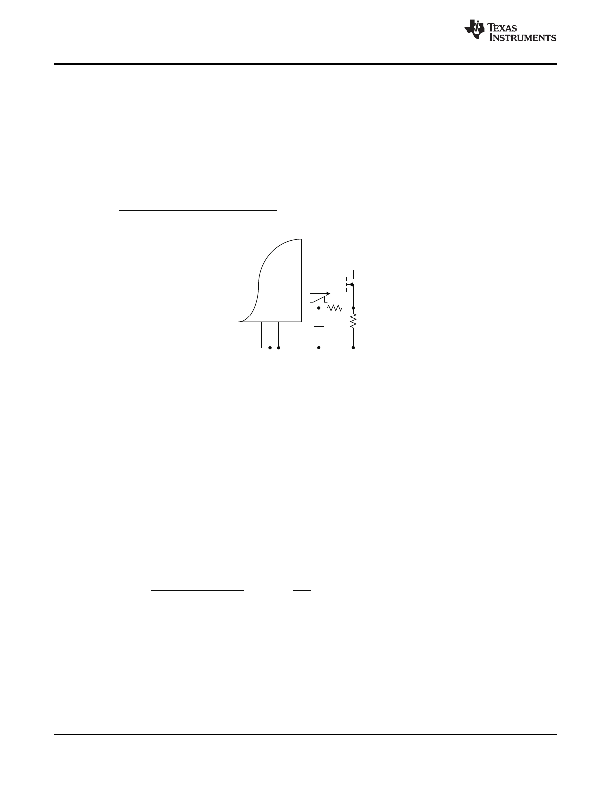
SLOPE
SLOPE_D
MAX
S
SL_EX
V (mV)
V (mV)
D
R ( ) = 1000
I ( A)
é ù
æ ö
-
ê úç ÷
ê ú
è ø
ë û
W ´
m
R
CS
GATE
CS
RTN
R
S
C
S
ARTN
COM
4 4
BLNK
SW
BIanking_Interval(%) 2
R (k ) = 10 = 10 = 80
f (kHz) 250
W ´ ´
TPS23754
TPS23754-1
TPS23756
SLVS885B – OCTOBER 2008 – REVISED MAY 2009 .......................................................................................................................................................
Current Slope Compensation
The TPS23754 provides a fixed internal compensation ramp that suffices for most applications. R
Figure 31 ) may be used if the internally provided slope compensation is not enough.
Most current-mode control papers and application notes define the slope values in terms of V
voltage / switching period), however the electrical characteristics table specifies the slope peak (V
on the maximum (78%) duty cycle. Assuming that the desired slope, V
period, compute R
per the following equation where V
S
SLOPE
SLOPE-D
, D
MAX
(in mV/period), is based on the full
, and I
are from the electrical
SL-EX
characteristics table with voltages in mV, current in µ A, and the duty cycle is unitless (e.g., D
/T
PP
S
SLOPE
= 0.78).
MAX
www.ti.com
(see
S
(peak ramp
) based
Figure 31. Additional Slope Compensation
C
may be required if the presence of R
S
appear at the C
Blanking Period, R
pin.
S
BLNK
causes increased noise, due to adjacent signals like the gate drive, to
S
Selection of the blanking period is often empirical because it is affected by parasitics and thermal effects of every
device between the gate-driver and output capacitors. The minimum blanking period prevents the current limit
and PWM comparators from being falsely triggered by the inherent current spike that occurs when the switching
MOSFET turns on. The maximum blanking period is bounded by the output rectifier's ability to withstand the
currents experienced during a converter output short.
If blanking beyond the internal default is desired choose R
using R
BLNK
(k Ω ) = t
BLNK
(ns).
BLNK
1. For a 100 ns blanking interval
a. R
b. Choose R
(k Ω ) = 100
BLNK
BLNK
= 100 k Ω .
The blanking interval can also be chosen as a percentage of the switching period.
1. Compute R
as follows for 2% blanking interval in a switcher running at 250 kHz.
BLNK
a.
b. Select R
Dead Time Resistor, R
BLNK
= 80.6 k Ω .
DT
The required dead time period depends on the specific topology and parasitics. The easiest technique to obtain
the optimum timing resistor is to build the supply and tune the dead time to achieve the best efficiency after
considering all corners of operation (load, input voltage, and temperature). A good initial value is 100 ns.
Program the dead time with a resistor connected from DT to ARTN per Equation 3 .
1. Choose R
as follows assuming a tDTof 100 ns:
DT
28 Submit Documentation Feedback Copyright © 2008 – 2009, Texas Instruments Incorporated
Product Folder Link(s): TPS23754 TPS23754-1 TPS23756

DT
DT
t (ns)
100
R (k ) = = = 50
2 2
W
C C
GATE C SW GATE GAT2 C SW GATE2
QG QG
V V
P = V f Q P = V f Q
V V
æ ö æ ö
´ ´ ´ ´ ´ ´
ç ÷ ç ÷
ç ÷ ç ÷
è ø è ø
GATE
12
P = 12 V 250 kHz 17 nC = 61.2 mW
10
´ ´ ´
G AT2
12
P = 12 V 250 kHz 8 nC = 28.8 mW
10
´ ´ ´
DRIVE
DRIVE
C
P
90 m W
I = = = 7.5 m A
V 12 V
STARTUP TOTAL
VC1 VC2
CUVH
T I
4 ms 8.42 mA
C + C = = = 5.18 F
V 6.5 V
´
´
m
VC1 CUV
ST
VC
C V
10.47 F 15 V
T = = = 39 ms
I 4 m A
´
m ´
VC1 VC2 CUVH
RECHARGE
VC
(C + C ) V
(10 F + 0.47 F) 6.5 V
T = = = 17 ms
I 4 mA
´
m m ´
VC1 VC2 CUVH
DISCHARGE
TOTAL
(C + C ) V
(10 F + 0.47 F) 6.5V
T = = = 8.08 ms
I 8.42 m A
´
m m ´
DISCHARGE
DISCHARGE RECHARGE
T
8.08 ms
Duty Cycle: D = = = 32%
T + T 8.08 ms + 17 ms
DISCHARGE RECHARGE
1 1
Hiccup Frequency: F = = = 39.9 Hz
T + T 8.08 ms + 17 ms
www.ti.com
a.
b. Choose R
TPS23754
TPS23754-1
TPS23756
....................................................................................................................................................... SLVS885B – OCTOBER 2008 – REVISED MAY 2009
= 49.9 k Ω
DT
Estimating Bias Supply Requirements and C
The bias supply (V
) power requirements determine the C
C
VC
sizing and frequency of hiccup during a fault. The
VC
first step is to determine the power/current requirements of the power supply control, then use this to select C
The control current draw will be assumed constant with voltage to simplify the estimate, resulting in an
approximate value.
First determine the switching MOSFET gate drive power.
1. Let V
be the gate voltage swing that the MOSFET Q
QG
is rated to (often 10 V).
G
a.
b. Compute gate drive power if V
is 12 V, Q
C
is 17 nC, and Q
GATE
is 8 nC.
GAT2
c.
P
d. This illustrates why MOSFET Q
= 61.2 mW + 28.8 mW = 90 mW
DRIVE
should be an important consideration in selecting the switching
G
MOSFETs.
2. Estimate the required bias current at some intermediate voltage during the C
discharge. For the
VC
TPS23754, 12 V provides a reasonable estimate. Add the operating bias current to the gate drive current.
a.
b. I
3. Compute the required C
= I
TOTAL
+ I
DRIVE
OPERATING
VC
= 7.5 mA + 0.92 mA = 8.42 mA
based on startup within the typical softstart period of 4 ms.
.
VC
a.
b. For this case, a standard 10 µ F electrolytic plus a 0.47 µ F should be sufficient.
4. Compute the initial time to start the converter when operating from PoE.
a. Using a typical bootstrap current of 4 mA, compute the time to startup.
b.
5. Compute the fault duty cycle and hiccup frequency
a.
b.
a. Note that the optocoupler current is 0 mA because the output is in current limit.
b. Also, it is assumed I
is 0 mA.
T2P
c.
d.
6. With the TPS23754, the voltage rating of C
and C
VC1
should be 25 V minimum while with the TPS23756
VC2
the rating can be 16 V.
Copyright © 2008 – 2009, Texas Instruments Incorporated Submit Documentation Feedback 29
Product Folder Link(s): TPS23754 TPS23754-1 TPS23756

D
VC1
C
VC
ARTN
R
VC
V
C
T1
BiasWinding
V
C
T2P From
TPS23754
R
T2P
R
T2P_OUT
Type2PSE
Indicator
V
OUT
Low= T2
OUT T2P-OUT
RT2P-OUT
T2P-OUT
V V (low)
5 0.4
I = = = 0.46 m A
R 10000
-
-
TPS23754
TPS23754-1
TPS23756
SLVS885B – OCTOBER 2008 – REVISED MAY 2009 .......................................................................................................................................................
www.ti.com
Switching Transformer Considerations and R
Care in design of the transformer and V
Leading-edge voltage overshoot on the bias winding may cause V
C
VC
bias circuit is required to obtain hiccup overload protection.
to peak-charge, preventing the expected
C
tracking with output voltage. Some method of controlling this is usually required. This may be as simple as a
series resistor, or an R-C filter in front of D
. Good transformer bias-to-output-winding coupling results in
VC1
reduced overshoot and better voltage tracking.
R
as shown in Figure 32 helps to reduce peak charging from the bias winding. This becomes especially
VC
important when tuning hiccup mode operation during output overload. Typical values for R
will be between 10
VC
Ω and 100 Ω .
Figure 32. R
Usage
VC
T2P Pin Interface
The T2P pin is an active low, open-drain output indicating a high power source is available. An optocoupler is
typically used to interface with the T2P pin to signal equipment on the secondary side of the converter of T2P
status. Optocoupler current-gain is referred to as CTR (current transfer ratio), which is the ratio of transistor
collector current to LED current. To preserve efficiency, a high-gain optocoupler ( 250% ≤ CTR ≤ 500%, or 300%
≤ CTR ≤ 600% ) along with a high-impedance (e.g., CMOS) receiver are recommended. Design of the T2P
optocoupler interface can be accomplished as follows:
1. T2P ON characteristic: I
2. Let V
= 12 V, V
C
= 5 V, R
OUT
= 2 mA minimum, V
T2P
T2P-OUT
= 10 k Ω , V
a.
3. The optocoupler CTR will be needed to determine R
LED bias current is selected. CTR will also vary with temperature and LED bias current. The strong variation
of CTR with diode current makes this a problem that requires some iteration using the CTR versus I
curve on the optocoupler data sheet.
a. Using the (normalized) curves, a current of 0.4 mA to 0.5 mA is required to support the output current at
the minimum CTR at 25 ° C.
a. Pick an I
. For example one around the desired load current.
DIODE
b. Use the optocoupler datasheet curve to determine the effective CTR at this operating current. It is
b. This manufacturer ’ s curves also indicate a – 20% variation of CTR with temperature. The approximate
30 Submit Documentation Feedback Copyright © 2008 – 2009, Texas Instruments Incorporated
usually necessary to apply the normalized curve value to the minimum specified CTR. It might be
necessary to ratio or offset the curve readings to obtain a value that is relative to the current that the
CTR is specified at.
c. If I
× CTR
DIODE
I_DIODE
is substantially different from I
Product Folder Link(s): TPS23754 TPS23754-1 TPS23756
Figure 33. T2P Interface
= 1 V
T2P
T2P-OUT
(low) = 400 mV max
. A device with a minimum CTR of 300% at 5 mA
T2P
RT2P_OUT
, choose another I
and repeat.
DIODE
DIODE

RT2P MIN
TEMP
100 1 00
I I = 0.5 m A = 0.625 m A
100 CTR 100 2 0
@ ´ ´
- D -
C T2P FLED
T2P
RT2P
V V V
12 1 1.1
R = = = 1 5.48 k
I 0.62 5 mA
- -
- W
C
1
0.1uF
R
DEN
R
CLS
From Ethernet
Transformers
V
DD
V
SS
CLS
From Spare
Pairs or
Transformers
DEN
PPD
D
VDD
V
DD1
RTN
COM
ARTN
C
IN
D
A
Adapter
R
APD2
R
APD1
APD
1.8kW
24V
D
1
58V
R
DEN
R
CLS
V
DD
V
SS
CLS
DEN
PPD
D
VDD
V
DD1
RTN
COM
ARTN
C
IN
D
A
Adapter
APD
R
HLD
1.8KW
D
HLD
24V
D
APD
30V
R
APD1
26.7kW
R
APD2
3.01kW
R
VDD1
3.3MW
For48V
Adapter
D
RT
N
58V
C
VDD
10nF
TPS23754
TPS23754-1
TPS23756
www.ti.com
....................................................................................................................................................... SLVS885B – OCTOBER 2008 – REVISED MAY 2009
forward voltage of the optocoupler diode is 1.1 V from the data sheet.
c. V
≈ 1.1 V
FLED
d. Select a 15.4 k Ω resistor. Even though the minimum CTR and temperature variation were considered,
the designer might choose a smaller resistor for a little more margin.
Advanced ORing Techniques
See Advanced Adapter ORing Solutions using the TSP23753, TI document number SLVA306A for ORing
applications that also work with the TPS23754. The material in sections Adapter ORing and Protection, D1 are
important to consider as well. The following applications are unique to the TPS23754 with the introduction of
PPD.
Option 2 ORing with PoE acting as a hot backup is eased by connecting PPD to V
connection enables the class regulator even when APD is high. The R-Zener network (1.8 k Ω – 24 V) is the
simplest circuit that will satisfy MPS requirements, keeping the PSE online. This network may be switched out
when the APD is not powered with an optocoupler. This works best with a 48-V adapter and the
APD-programmed threshold as high as possible. An example of an adapter priority application with smooth
switchover between a 48 V adapter and PoE is shown on the right side of Figure 34 . D
effective APD hysteresis, allowing the PSE to power the load before V
-V
VDD1
RTN
hotswap foldback.
per Figure 34 . This PPD
DD
is used to reduce the
APD
falls too low and causes a
Figure 34. Option 2 PoE Backup ORing
Option 1 ORing of a low voltage adapter (e.g., 24 V) is possible by connecting a resistor divider to PPD as in
Figure 35 . When 1.55 V ≤ V
≤ 8.3 V, the hotswap MOSFET is enabled, T2P is activated, and the class
PPD
feature is disabled. The hotswap current limit is unaffected, limiting the available power. For example, the
maximum input power from a 24 V adapter would be 19.3 W [(24 V – 0.6 V) × 0.825 A].
Copyright © 2008 – 2009, Texas Instruments Incorporated Submit Documentation Feedback 31
Product Folder Link(s): TPS23754 TPS23754-1 TPS23756

RTN
D
1
58V
C
1
0.1uF
R
DEN
R
CLS
From Ethernet
Transformers
V
DD
V
SS
CLS
From Spare
Pairs or
Transformers
DEN
D
A
Adapter
PPD
R
PPD2
R
PPD1
V
DD1
COM
ARTN
APD
R
FBU
R
FBL
TLV431
R
OB
C
IZ
R
SS
C
SS
D
SS
FromRegulated
OutputVoltage
TPS23754
TPS23754-1
TPS23756
SLVS885B – OCTOBER 2008 – REVISED MAY 2009 .......................................................................................................................................................
Figure 35. Low-Voltage Option 1 ORing
www.ti.com
Softstart
Converters require a softstart on the voltage error amplifier to prevent output overshoot on startup. Figure 36
shows a common implementation of a secondary-side softstart that works with the typical TL431 error amplifier.
The softstart components consist of D
V
down as C
CTL
output and C
charges through R
SS
are preset to the proper value as the output voltage reaches the regulated value, preventing
IZ
voltage overshoot due to the error amplifier recovery. The secondary-side error amplifier will not become active
until there is sufficient voltage on the secondary. The TPS23754 provides a primary-side softstart which persists
long enough (~4 ms) for secondary side voltage-loop softstart to take over. The primary-side current-loop
softstart controls the switching MOSFET peak current by applying a slowly rising ramp voltage to a second PWM
control input. The PWM is controlled by the lower of the softstart ramp or the CTL-derived current demand. The
actual output voltage rise time is usually much shorter than the internal softstart period. Initially the internal
softstart ramp limits the maximum current demand as a function of time. Either the current limit, secondary-side
softstart, or output regulation assume control of the PWM before the internal softstart period is over. Figure 25
shows a smooth handoff between the primary and secondary-side softstart with minimal output voltage
overshoot.
, R
SS
, and C
SS
, the optocoupler, and D
OB
. They serve to control the output rate-of-rise by pulling
SS
. This has the added advantage that the TL431
SS
32 Submit Documentation Feedback Copyright © 2008 – 2009, Texas Instruments Incorporated
Figure 36. Error Amplifier Soft Start
Product Folder Link(s): TPS23754 TPS23754-1 TPS23756

+
-
49.9kW
10kW4.99kW
6.04kW
10kW
0.01mF
301kW
1 Fm
V
B
To
FRS
ARTN
TL331IDBV
TPS23754
TPS23754-1
TPS23756
www.ti.com
Special Switching MOSFET Considerations
Special care must be used in selecting the converter switching MOSFET. The TPS23756 minimum switching
MOSFET V
towards the end of a (failed) bootstrap startup. The MOSFET must be able to carry the anticipated peak fault
current at this gate voltage.
Thermal Considerations and OTSD
Sources of nearby local PCB heating should be considered during the thermal design. Typical calculations
assume that the TPS23754 is the only heat source contributing to the PCB temperature rise. It is possible for a
normally operating TPS23754 device to experience an OTSD event if it is excessively heated by a nearby
device.
Frequency Dithering for Conducted Emissions Control
The international standard CISPR 22 (and adopted versions) is often used as a requirement for conducted
emissions. Ethernet cables are covered as a telecommunication port under section 5.2 for conducted emissions.
Meeting EMI requirements is often a challenge, with the lower limits of Class B being especially hard. Circuit
board layout, filtering, and snubbing various nodes in the power circuit are the first layer of control techniques. A
more detailed discussion of EMI control is presented in Practical Guidelines to Designing an EMI Compliant PoE
Powered Device With Isolated Flyback, TI literature number SLUA469 . Additionally, IEEE802.3-2005 sections
33.3 and 33.4 have requirements for noise injected onto the Ethernet cable based on compatibility with data
transmission.
Occasionally, a technique referred to as frequency dithering is utilized to provide additional EMI measurement
reduction. The switching frequency is modulated to spread the narrowband individual harmonics across a wider
bandwidth, thus lowering peak measurements. The circuit of Figure 37 modulates the switching frequency by
feeding a small ac signal into the FRS pin. These values may be adapted to suit individual needs.
....................................................................................................................................................... SLVS885B – OCTOBER 2008 – REVISED MAY 2009
is ~5.5 V, which is due to the V
GATE
lower threshold. This will occur during an output overload, or
C
Figure 37. Frequency Dithering
ESD
The TPS23754 has been tested to EN61000-4-2 using a power supply based on Figure 1 . The levels used were
8 kV contact discharge and 15 kV air discharge. Surges were applied between the PoE input and the dc output,
between the adapter input and the dc output, between the adapter and the PoE inputs, and to the dc output with
respect to earth. Tests were done both powered and unpowered. No TPS23754 failures were observed and
operation was continuous. See Figure 29 for additional protection for some test configurations.
ESD requirements for a unit that incorporates the TPS23754 have a much broader scope and operational
implications than are used in TI ’ s testing. Unit-level requirements should not be confused with reference design
testing that only validates the ruggedness of the TPS23754.
Layout
Printed circuit board layout recommendations are provided in the evaluation module (EVM) documentation
available for these devices.
Copyright © 2008 – 2009, Texas Instruments Incorporated Submit Documentation Feedback 33
Product Folder Link(s): TPS23754 TPS23754-1 TPS23756

TPS23754
TPS23754-1
TPS23756
SLVS885B – OCTOBER 2008 – REVISED MAY 2009 .......................................................................................................................................................
Changes from Revision A (April 2009) to Revision B .................................................................................................... Page
• Deleted The TPS23756 is at PREVIEW status. .................................................................................................................... 1
• Changed Preview ................................................................................................................................................................... 2
• Changed minimum limit ........................................................................................................................................................ 3
• Changed limits ....................................................................................................................................................................... 3
• Added graph for 756 ............................................................................................................................................................ 12
• Added graph for 756 ............................................................................................................................................................ 12
• Added graph for ' 756 ........................................................................................................................................................... 13
www.ti.com
34 Submit Documentation Feedback Copyright © 2008 – 2009, Texas Instruments Incorporated
Product Folder Link(s): TPS23754 TPS23754-1 TPS23756

PACKAGE OPTION ADDENDUM
www.ti.com 9-Jun-2009
PACKAGING INFORMATION
Orderable Device Status
(1)
Package
Type
Package
Drawing
Pins Package
Qty
Eco Plan
TPS23754PWP ACTIVE HTSSOP PWP 20 70 Green (RoHS &
(2)
Lead/Ball Finish MSL Peak Temp
CU NIPDAU Level-2-260C-1 YEAR
(3)
no Sb/Br)
TPS23754PWP-1 ACTIVE HTSSOP PWP 20 70 Green (RoHS &
CU NIPDAU Level-2-260C-1 YEAR
no Sb/Br)
TPS23754PWPR ACTIVE HTSSOP PWP 20 2000 Green (RoHS &
CU NIPDAU Level-2-260C-1 YEAR
no Sb/Br)
TPS23754PWPR-1 ACTIVE HTSSOP PWP 20 2000 Green (RoHS &
CU NIPDAU Level-2-260C-1 YEAR
no Sb/Br)
TPS23756PWP ACTIVE HTSSOP PWP 20 70 Green (RoHS &
CU NIPDAU Level-2-260C-1 YEAR
no Sb/Br)
TPS23756PWPR ACTIVE HTSSOP PWP 20 2000 Green (RoHS &
CU NIPDAU Level-2-260C-1 YEAR
no Sb/Br)
(1)
The marketing status values are defined as follows:
ACTIVE: Product device recommended for new designs.
LIFEBUY: TI has announced that the device will be discontinued, and a lifetime-buy period is in effect.
NRND: Not recommended for new designs. Device is in production to support existing customers, but TI does not recommend using this part in
a new design.
PREVIEW: Device has been announced but is not in production. Samples may or may not be available.
OBSOLETE: TI has discontinued the production of the device.
(2)
Eco Plan - The planned eco-friendly classification: Pb-Free (RoHS), Pb-Free (RoHS Exempt), or Green (RoHS & no Sb/Br) - please check
http://www.ti.com/productcontent for the latest availability information and additional product content details.
TBD: The Pb-Free/Green conversion plan has not been defined.
Pb-Free (RoHS): TI's terms "Lead-Free" or "Pb-Free" mean semiconductor products that are compatible with the current RoHS requirements
for all 6 substances, including the requirement that lead not exceed 0.1% by weight in homogeneous materials. Where designed to be soldered
at high temperatures, TI Pb-Free products are suitable for use in specified lead-free processes.
Pb-Free (RoHS Exempt): This component has a RoHS exemption for either 1) lead-based flip-chip solder bumps used between the die and
package, or 2) lead-based die adhesive used between the die and leadframe. The component is otherwise considered Pb-Free (RoHS
compatible) as defined above.
Green (RoHS & no Sb/Br): TI defines "Green" to mean Pb-Free (RoHS compatible), and free of Bromine (Br) and Antimony (Sb) based flame
retardants (Br or Sb do not exceed 0.1% by weight in homogeneous material)
(3)
MSL, Peak Temp. -- The Moisture Sensitivity Level rating according to the JEDEC industry standard classifications, and peak solder
temperature.
Important Information and Disclaimer:The information provided on this page represents TI's knowledge and belief as of the date that it is
provided. TI bases its knowledge and belief on information provided by third parties, and makes no representation or warranty as to the
accuracy of such information. Efforts are underway to better integrate information from third parties. TI has taken and continues to take
reasonable steps to provide representative and accurate information but may not have conducted destructive testing or chemical analysis on
incoming materials and chemicals. TI and TI suppliers consider certain information to be proprietary, and thus CAS numbers and other limited
information may not be available for release.
In no event shall TI's liability arising out of such information exceed the total purchase price of the TI part(s) at issue in this document sold by TI
to Customer on an annual basis.
Addendum-Page 1
PACKAGE MATERIALS INFORMATION
www.ti.com 5-Jun-2009
TAPE AND REEL INFORMATION
*All dimensions are nominal
Device Package
TPS23754PWPR HTSSOP PWP 20 2000 330.0 16.4 6.95 7.1 1.6 8.0 16.0 Q1
TPS23754PWPR-1 HTSSOP PWP 20 2000 330.0 16.4 6.95 7.1 1.6 8.0 16.0 Q1
TPS23756PWPR HTSSOP PWP 20 2000 330.0 16.4 6.95 7.1 1.6 8.0 16.0 Q1
Type
Package
Drawing
Pins SPQ Reel
Diameter
(mm)
Reel
Width
W1 (mm)
A0 (mm) B0 (mm) K0 (mm) P1
(mm)W(mm)
Pin1
Quadrant
Pack Materials-Page 1

PACKAGE MATERIALS INFORMATION
www.ti.com 5-Jun-2009
*All dimensions are nominal
Device Package Type Package Drawing Pins SPQ Length (mm) Width (mm) Height (mm)
TPS23754PWPR HTSSOP PWP 20 2000 346.0 346.0 33.0
TPS23754PWPR-1 HTSSOP PWP 20 2000 346.0 346.0 33.0
TPS23756PWPR HTSSOP PWP 20 2000 346.0 346.0 33.0
Pack Materials-Page 2
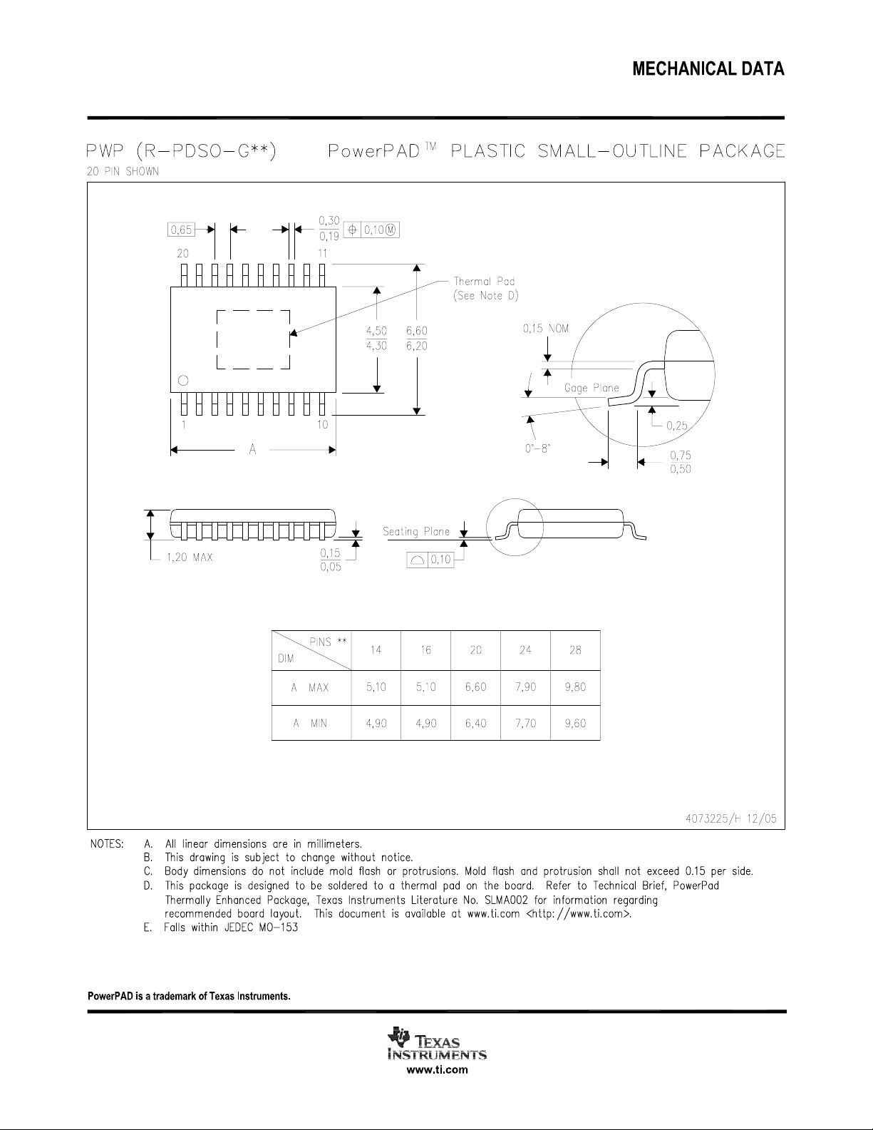


IMPORTANT NOTICE
Texas Instruments Incorporated and its subsidiaries (TI) reserve the right to make corrections, modifications, enhancements, improvements,
and other changes to its products and services at any time and to discontinue any product or service without notice. Customers should
obtain the latest relevant information before placing orders and should verify that such information is current and complete. All products are
sold subject to TI’s terms and conditions of sale supplied at the time of order acknowledgment.
TI warrants performance of its hardware products to the specifications applicable at the time of sale in accordance with TI’s standard
warranty. Testing and other quality control techniques are used to the extent TI deems necessary to support this warranty. Except where
mandated by government requirements, testing of all parameters of each product is not necessarily performed.
TI assumes no liability for applications assistance or customer product design. Customers are responsible for their products and
applications using TI components. To minimize the risks associated with customer products and applications, customers should provide
adequate design and operating safeguards.
TI does not warrant or represent that any license, either express or implied, is granted under any TI patent right, copyright, mask work right,
or other TI intellectual property right relating to any combination, machine, or process in which TI products or services are used. Information
published by TI regarding third-party products or services does not constitute a license from TI to use such products or services or a
warranty or endorsement thereof. Use of such information may require a license from a third party under the patents or other intellectual
property of the third party, or a license from TI under the patents or other intellectual property of TI.
Reproduction of TI information in TI data books or data sheets is permissible only if reproduction is without alteration and is accompanied
by all associated warranties, conditions, limitations, and notices. Reproduction of this information with alteration is an unfair and deceptive
business practice. TI is not responsible or liable for such altered documentation. Information of third parties may be subject to additional
restrictions.
Resale of TI products or services with statements different from or beyond the parameters stated by TI for that product or service voids all
express and any implied warranties for the associated TI product or service and is an unfair and deceptive business practice. TI is not
responsible or liable for any such statements.
TI products are not authorized for use in safety-critical applications (such as life support) where a failure of the TI product would reasonably
be expected to cause severe personal injury or death, unless officers of the parties have executed an agreement specifically governing
such use. Buyers represent that they have all necessary expertise in the safety and regulatory ramifications of their applications, and
acknowledge and agree that they are solely responsible for all legal, regulatory and safety-related requirements concerning their products
and any use of TI products in such safety-critical applications, notwithstanding any applications-related information or support that may be
provided by TI. Further, Buyers must fully indemnify TI and its representatives against any damages arising out of the use of TI products in
such safety-critical applications.
TI products are neither designed nor intended for use in military/aerospace applications or environments unless the TI products are
specifically designated by TI as military-grade or "enhanced plastic." Only products designated by TI as military-grade meet military
specifications. Buyers acknowledge and agree that any such use of TI products which TI has not designated as military-grade is solely at
the Buyer's risk, and that they are solely responsible for compliance with all legal and regulatory requirements in connection with such use.
TI products are neither designed nor intended for use in automotive applications or environments unless the specific TI products are
designated by TI as compliant with ISO/TS 16949 requirements. Buyers acknowledge and agree that, if they use any non-designated
products in automotive applications, TI will not be responsible for any failure to meet such requirements.
Following are URLs where you can obtain information on other Texas Instruments products and application solutions:
Products Applications
Amplifiers amplifier.ti.com Audio www.ti.com/audio
Data Converters dataconverter.ti.com Automotive www.ti.com/automotive
DLP® Products www.dlp.com Broadband www.ti.com/broadband
DSP dsp.ti.com Digital Control www.ti.com/digitalcontrol
Clocks and Timers www.ti.com/clocks Medical www.ti.com/medical
Interface interface.ti.com Military www.ti.com/military
Logic logic.ti.com Optical Networking www.ti.com/opticalnetwork
Power Mgmt power.ti.com Security www.ti.com/security
Microcontrollers microcontroller.ti.com Telephony www.ti.com/telephony
RFID www.ti-rfid.com Video & Imaging www.ti.com/video
RF/IF and ZigBee® Solutions www.ti.com/lprf Wireless www.ti.com/wireless
Mailing Address: Texas Instruments, Post Office Box 655303, Dallas, Texas 75265
Copyright © 2009, Texas Instruments Incorporated
 Loading...