

TPS2010, TPS2011, TPS2012, TPS2013
POWER-DISTRIBUTION
SLVS097A – DECEMBER 1994 – REVISED AUGUST 1995
1
POST OFFICE BOX 655303 • DALLAS, TEXAS 75265
D
95-mΩ Max (5.5-V Input) High-Side MOSFET
Switch With Logic Compatible Enable Input
D
Short-Circuit and Thermal Protection
D
Typical Short-Circuit Current Limits:
0.4 A, TPS2010; 1.2 A, TPS2011;
2 A, TPS2012; 2.6 A, TPS2013
D
Electrostatic-Discharge Protection, 12-kV
Output, 6-kV All Other Terminals
D
Controlled Rise and Fall Times to Limit
Current Surges and Minimize EMI
D
SOIC-8 Package Pin Compatible With the
Popular Littlefoot Series When GND Is
Connected
D
2.7-V to 5.5-V Operating Range
D
10-µA Maximum Standby Current
D
Surface-Mount SOIC-8 and TSSOP-14
Packages
D
–40°C to 125°C Operating Junction
T emperature Range
description
The TPS201x family of power-distribution switches is intended for applications where heavy capacitive loads
and short circuits are likely to be encountered. The high-side switch is a 95-mΩ N-channel MOSFET . Gate drive
is provided by an internal driver and charge pump designed to control the power switch rise times and fall times
to minimize current surges during switching. The charge pump operates at 100 kHz, requires no external
components, and allows operation from supplies as low as 2.7 V . When the output load exceeds the current-limit
threshold or a short circuit is present, the TPS201x limits the output current to a safe level by switching into a
constant-current mode. Continuous heavy overloads and short circuits increase power dissipation in the switch
and cause the junction temperature to rise. If the junction temperature reaches approximately 180°C, a thermal
protection circuit shuts the switch off to prevent damage. Recovery from thermal shutdown is automatic once
the device has cooled sufficiently.
The members of the TPS201x family differ only in short-circuit current threshold. The TPS2010 is designed to
limit at 0.4-A load; the other members of the family limit at 1.2 A, 2 A, and 2.6 A (see the available options table).
The TPS201x family is available in 8-pin small-outline integrated circuit (SOIC) and 14-pin thin shink
small-outline (TSSOP) packages and operates over a junction temperature range of –40°C to 125°C. Versions
in the 8-pin SOIC package are drop-in replacements for Siliconix’s Littlefoot power PMOS switches, except
that GND must be connected.
Copyright 1995, Texas Instruments Incorporated
PRODUCTION DATA information is current as of publication date.
Products conform to specifications per the terms of Texas Instruments
standard warranty. Production processing does not necessarily include
testing of all parameters.
Please be aware that an important notice concerning availability, standard warranty, and use in critical applications of
Texas Instruments semiconductor products and disclaimers thereto appears at the end of this data sheet.
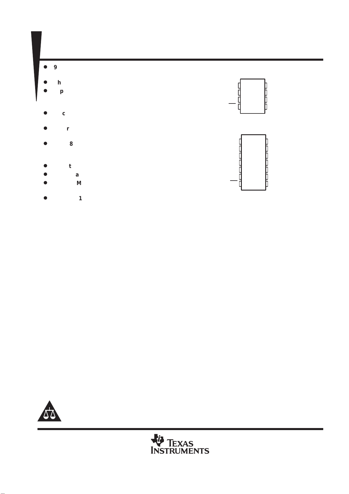
1
2
3
4
8
7
6
5
GND
IN
IN
EN
OUT
OUT
OUT
OUT
D PACKAGE
(TOP VIEW)
1
2
3
4
5
6
7
14
13
12
11
10
9
8
GND
IN
IN
IN
IN
IN
EN
OUT
OUT
OUT
OUT
OUT
OUT
OUT
PW PACKAGE
(TOP VIEW)
TPS2010, TPS2011, TPS2012, TPS2013
POWER-DISTRIBUTION
SLVS097A – DECEMBER 1994 – REVISED AUGUST 1995
2
POST OFFICE BOX 655303 • DALLAS, TEXAS 75265
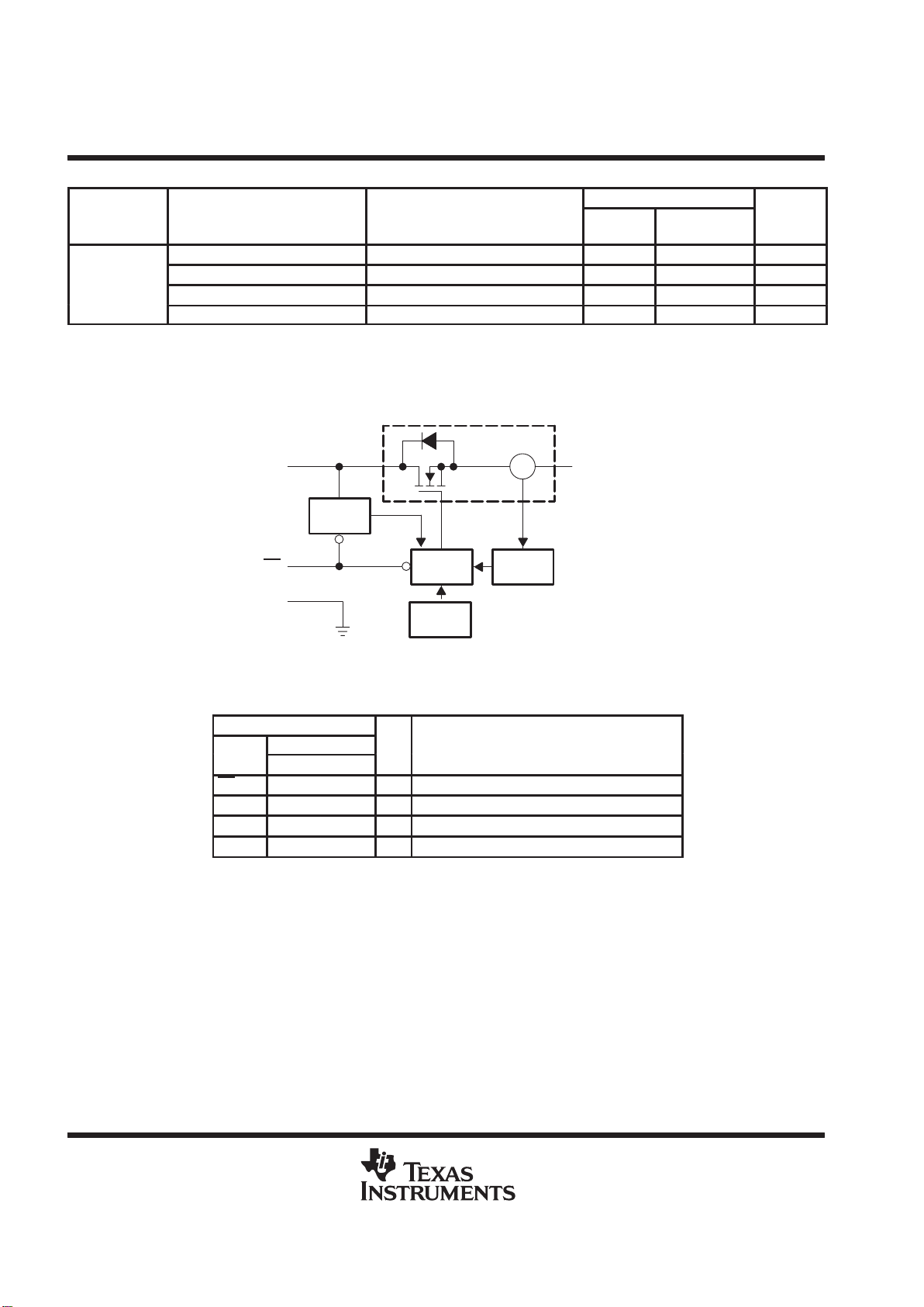
AVAILABLE OPTIONS
RECOMMENDED MAXIMUM TYPICAL SHORT-CIRCUIT
PACKAGED DEVICES
CHIP
T
J
CONTINUOUS LOAD CURRENT
(A)
OUTPUT CURRENT LIMIT AT 25°C
(A)
SOIC
(D)
†
TSSOP
(PW)
‡
FORM
(Y)
0.2 0.4 TPS2010D TPS2010PWLE TPS2010Y
°
°
0.6 1.2 TPS2011D TPS2011PWLE TPS2011Y
–
40°C to 125°C
1 2 TPS2012D TPS2012PWLE TPS2012Y
1.5 2.6 TPS2013D TPS2013PWLE TPS2013Y
†
The D package is available taped and reeled. Add an R suffix to device type (e.g., TPS2010DR).
‡
The PW package is only available left-end taped and reeled (indicated by the LE suffix on the device type; e.g., TPS2010PWLE).
functional block diagram
Power Switch
Current
Limit
Driver
Thermal
Sense
Charge
Pump
IN
EN
GND
OUT
CS
†
†
Current sense
Terminal Functions
TERMINAL
NO.
I/O DESCRIPTION
NAME
D PW
EN 4 7 I Enable input. Logic low turns power switch on.
GND 1 1 I Ground
IN 2, 3 2–6 I Input voltage
OUT 5–8 8–14 O Power-switch output
detailed description
power switch
The power switch is an N-channel MOSFET with a maximum on-state resistance of 95 mΩ (V
I(IN)
= 5.5 V),
configured as a high-side switch.
charge pump
An internal 100-kHz charge pump supplies power to the driver circuit and provides the necessary voltage to pull
the gate of the MOSFET above the source. The charge pump operates from input voltages as low as 2.7 V and
requires very little supply current.

TPS2010, TPS2011, TPS2012, TPS2013
POWER-DISTRIBUTION
SLVS097A – DECEMBER 1994 – REVISED AUGUST 1995
3
POST OFFICE BOX 655303 • DALLAS, TEXAS 75265
detailed description (continued)
driver
The driver controls the gate voltage of the power switch. T o limit large current surges and reduce the associated
electromagnetic interference (EMI) produced, the driver incorporates circuitry that controls the rise times and
fall times of the output voltage. The rise and fall times are typically in the 2-ms to 4-ms range instead of the
microsecond or nanosecond range for a standard FET.
enable (EN)
A logic high on the EN input turns off the power switch and the bias for the charge pump, driver , and other circuitry
to reduce the supply current to less than 10 µA. A logic zero input restores bias to the drive and control circuits
and turns the power on. The enable input is compatible with both TTL and CMOS logic levels.
current sense
A sense FET monitors the current supplied to the load. The sense FET is a much more efficient way to measure
current than conventional resistance methods. When an overload or short circuit is encountered, the
current-sense circuitry sends a control signal to the driver. The driver in turn reduces the gate voltage and drives
the power FET into its linear region, which switches the output into a constant current mode and simply holds
the current constant while varying the voltage on the load.
thermal sense
An internal thermal-sense circuit shuts the power switch off when the junction temperature rises to
approximately 180°C. Hysteresis is built into the thermal sense, and after the device has cooled approximately
20 degrees, the switch turns back on. The switch continues to cycle off and on until the fault is removed.
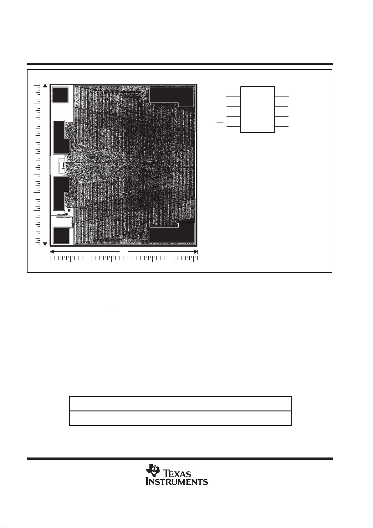
TPS201xY chip information
This chip, when properly assembled, displays characteristics similar to the TPS201xC. Thermal compression
or ultrasonic bonding may be used on the doped aluminum bonding pads. The chip may be mounted with
conductive epoxy or a gold-silicon preform.
TPS2010, TPS2011, TPS2012, TPS2013
POWER-DISTRIBUTION
SLVS097A – DECEMBER 1994 – REVISED AUGUST 1995
4
POST OFFICE BOX 655303 • DALLAS, TEXAS 75265
BONDING PAD ASSIGNMENTS
CHIP THICKNESS: 15 MILS TYPICAL
BONDING PADS: 4 × 4 MILS MINIMUM
TJmax = 150°C
TOLERANCES ARE ±10%
ALL DIMENSIONS ARE IN MILS
81
72
TPS201xY
(2)
(6)
(1)
(3)
(7)
(8)
(5)(4)
OUTGND
IN
IN
EN
OUT
OUT
OUT
(2)
(1)
(3)
(4)
(6)
(7)(8)
(5)
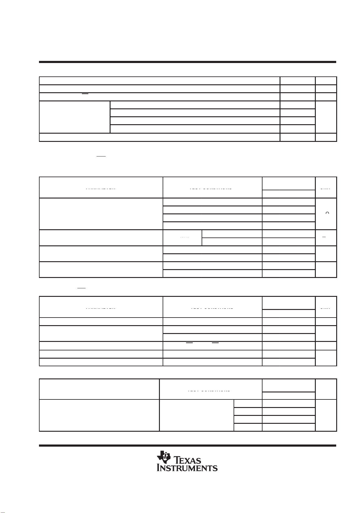
absolute maximum ratings over operating free-air temperature range (unless otherwise noted)
†
Input voltage range, V
I(IN)
(see Note 1) –0.3 V to 7 V. . . . . . . . . . . . . . . . . . . . . . . . . . . . . . . . . . . . . . . . . . . . . . .
Output voltage range, V
O
(see Note 1) –0.3 V to V
I(IN)
+0.3 V. . . . . . . . . . . . . . . . . . . . . . . . . . . . . . . . . . . . . . .
Input voltage range, VI at EN –0.3 V to 7 V. . . . . . . . . . . . . . . . . . . . . . . . . . . . . . . . . . . . . . . . . . . . . . . . . . . . . . . .
Continuous output current, IO internally limited. . . . . . . . . . . . . . . . . . . . . . . . . . . . . . . . . . . . . . . . . . . . . . . . . . . . .
Continuous total power dissipation See Dissipation Rating Table. . . . . . . . . . . . . . . . . . . . . . . . . . . . . . . . . . . . .
Operating virtual junction temperature range, T
J
–40°C to 125°C. . . . . . . . . . . . . . . . . . . . . . . . . . . . . . . . . . . .
Storage temperature range, T
stg
–65°C to 150°C. . . . . . . . . . . . . . . . . . . . . . . . . . . . . . . . . . . . . . . . . . . . . . . . . .
Lead temperature soldering 1,6 mm (1/16 inch) from case for 10 seconds 260°C. . . . . . . . . . . . . . . . . . . . . . .
†
Stresses beyond those listed under “absolute maximum ratings” may cause permanent damage to the device. These are stress ratings only, and
functional operation of the device at these or any other conditions beyond those indicated under “recommended operating conditions” is not
implied. Exposure to absolute-maximum-rated conditions for extended periods may affect device reliability.
NOTE 1: All voltages are with respect to GND.
DISSIPATION RATING TABLE
PACKAGE
TA ≤ 25°C
POWER RATING
DERATING FACTOR
ABOVE TA = 25°C
TA = 70°C
POWER RATING
TA = 125°C
POWER RATING
D 725 mW 5.8 mW/°C 464 mW 145 mW
PW 700 mW 5.6 mW/°C 448 mW 140 mW
TPS2010, TPS2011, TPS2012, TPS2013
POWER-DISTRIBUTION
SLVS097A – DECEMBER 1994 – REVISED AUGUST 1995
5
POST OFFICE BOX 655303 • DALLAS, TEXAS 75265
recommended operating conditions
MIN MAX UNIT
Input voltage, V
I(IN)
2.7 5.5 V
Input voltage, VI at EN 0 5.5 V
TPS2010 0 0.2
p
TPS2011 0 0.6
Continuous output current, I
O
TPS2012 0 1
A
TPS2013 0 1.5
Operating virtual junction temperature, T
J
–40 125 °C
electrical characteristics over recommended operating junction temperature range, V
I(IN)
= 5.5 V,
I
O
= rated current, EN = 0 V (unless otherwise noted)
power switch
PARAMETER
TEST CONDITIONS
†
TPS2010, TPS2011
TPS2012, TPS2013
UNIT
PARAMETER
TEST CONDITIONS
MIN TYP MAX
UNIT
V
I(IN)
= 5.5 V, TJ = 25°C 75 95
V
I(IN)
= 4.5 V, TJ = 25°C 80 110
On-state resistance
V
I(IN)
= 3 V, TJ = 25°C 120 175
mΩ
V
I(IN)
= 2.7 V, TJ = 25°C 140 215
p
TJ = 25°C 0.001 1
Output leakage current
EN
=
V
I(IN)
–40°C ≤ TJ ≤ 125°C 10
µ
A
p
V
I(IN)
= 5.5 V, TJ = 25°C, CL = 1 µF 4
trOutput rise time
V
I(IN)
= 2.7 V, TJ = 25°C, CL = 1 µF 3.8
ms
p
V
I(IN)
= 5.5 V, TJ = 25°C, CL = 1 µF 3.9
tfOutput fall time
V
I(IN)
= 2.7 V, TJ = 25°C, CL = 1 µF 3.5
ms
†
Pulse-testing techniques maintain junction temperature close to ambient temperature; thermal effects must be taken into account separately.
enable input (EN)
PARAMETER TEST CONDITIONS
TPS2010, TPS2011
TPS2012, TPS2013
UNIT
PARAMETER
TEST CONDITIONS
MIN TYP MAX
UNIT
High-level input voltage 2.7 V ≤ V
I(IN)
≤ 5.5 V 2 V
p
4.5 V ≤ V
I(IN)
≤ 5.5 V 0.8
Low-level input voltage
2.7 V ≤ V
I(IN)
< 4.5 V 0.4
V
Input current
EN = 0 V or EN = V
I(IN)
–0.5 0.5 µA
t
PLH
Propagation (delay) time, low-to-high-level output CL = 1 µF 20
t
PHL
Propagation (delay) time, high-to-low-level output CL = 1 µF 40
ms
current limit
PARAMETER
TEST CONDITIONS
†
TPS2010, TPS2011
TPS2012, TPS2013
UNIT
TEST CONDITIONS
MIN TYP MAX
°
TPS2010 0.22 0.4 0.6
T
J
=
25 C
,
V
I
(IN)
= 5.5 V,
TPS2011 0.66 1.2 1.8
Short-circuit current
I(IN)
OUT connected to GND, device
TPS2012 1.1 2 3
A
enabled into short circu
it
TPS2013 1.65 2.6 4.5
†
Pulse-testing techniques maintain junction temperature close to ambient temperature; thermal effects must be taken into account separately.
TPS2010, TPS2011, TPS2012, TPS2013
POWER-DISTRIBUTION
SLVS097A – DECEMBER 1994 – REVISED AUGUST 1995
6
POST OFFICE BOX 655303 • DALLAS, TEXAS 75265
electrical characteristics over recommended operating junction temperature range, V
I(IN)
= 5.5 V,
I
O
= rated current, EN = 0 V (unless otherwise noted) (continued)
supply current
PARAMETER TEST CONDITIONS
TPS2010, TPS2011
TPS2012, TPS2013
UNIT
PARAMETER
TEST CONDITIONS
MIN TYP MAX
UNIT
pp
p
TJ = 25°C 0.015 1
Supply current, low-level output
EN
=
V
I(IN)
–40°C ≤ TJ ≤ 125°C 10
µ
A
pp
p
TJ = 25°C 73 100
Supply current, high-level output
EN
= 0
V
–40°C ≤ TJ ≤ 125°C 100
µ
A
electrical characteristics over recommended operating junction temperature range, V
I(IN)
= 5.5 V,
I
O
= rated current, EN = 0 V, TJ = 25°C (unless otherwise noted)
power switch
PARAMETER
TEST CONDITIONS
†
TPS2010Y, TPS201 1Y
TPS2012Y, TPS2013Y
UNIT
PARAMETER
TEST CONDITIONS
MIN TYP MAX
UNIT
V
I(IN)
= 5.5 V, 75
V
I(IN)
= 4.5 V, 80
On-state resistance
V
I(IN)
= 3 V, 120
mΩ
V
I(IN)
= 2.7 V, 140
Output leakage current
EN = V
I(IN)
0.001 µA
p
V
I(IN)
= 5.5 V, CL = 1 µF 4
Output rise time
V
I(IN)
= 2.7 V, CL = 1 µF 3.8
ms
p
V
I(IN)
= 5.5 V, CL = 1 µF 3.9
Output fall time
V
I(IN)
= 2.7 V, CL = 1 µF 3.5
ms
†
Pulse-testing techniques maintain junction temperature close to ambient temperature; thermal effects must be taken into account separately.
current limit
PARAMETER
TEST CONDITIONS
†
TPS2010Y, TPS201 1Y
TPS2012Y, TPS2013Y
UNIT
MIN TYP MAX
Short-circuit current
V
I(IN)
= 5.5 V,
OUT connected to GND,
Device enabled into short circuit
0.4 A
†
Pulse-testing techniques maintain junction temperature close to ambient temperature; thermal effects must be taken into account separately.
supply current
PARAMETER TEST CONDITIONS
TPS2010Y, TPS201 1Y
TPS2012Y, TPS2013Y
UNIT
PARAMETER
TEST CONDITIONS
MIN TYP MAX
UNIT
Supply current, low-level output
EN = V
I(IN)
0.015 µA
Supply current, high-level output
EN = 0 V
73 µA
TPS2010, TPS2011, TPS2012, TPS2013
POWER-DISTRIBUTION
SLVS097A – DECEMBER 1994 – REVISED AUGUST 1995
7
POST OFFICE BOX 655303 • DALLAS, TEXAS 75265
PARAMETER MEASUREMENT INFORMATION
Figure 1. Propagation Delay and
Rise Time With 1-µF Load, V
I(IN)
= 5.5 V
0123456789
t – Time – ms
6
4
2
0
6
4
2
0
Enable Voltage – VV
O
– Output Voltage – V
–1
Figure 2. Propagation Delay and
Fall Time With 1-µF Load, V
I(IN)
= 5.5 V
0 5 10 15 20 25 30 35 40 45
t – Time – ms
Enable Voltage – V
6
4
2
0
6
4
2
0
V
O
– Output Voltage – V
–1
Figure 3. Propagation Delay and
Rise Time With 1-µF Load, V
I(IN)
= 2.7 V
0123456789
t – Time – ms
4
2
0
4
2
0
Enable Voltage – VV
O
– Output Voltage – V
–1
Figure 4. Propagation Delay and
Fall Time With 1-µF Load, V
I(IN)
= 2.7 V
0 5 10 15 20 25 30 35 40 45
t – Time – ms
4
2
0
4
2
0
Enable Voltage – VV
O
– Output Voltage – V
–1

TPS2010, TPS2011, TPS2012, TPS2013
POWER-DISTRIBUTION
SLVS097A – DECEMBER 1994 – REVISED AUGUST 1995
8
POST OFFICE BOX 655303 • DALLAS, TEXAS 75265
PARAMETER MEASUREMENT INFORMATION
Figure 5. TPS2010, Short-Circuit Current.
Short is Applied to Enabled Device, V
I(IN)
= 5.5 V
01234
t – Time – ms
0.5 1.5 2.5 3.5 4.5
5
0
6
4
2
0
8
V
O
– Output Voltage – VI
O
– Output Current – A
–1
Figure 6. TPS2011, Short-Circuit Current.
Short is Applied to Enabled Device, V
I(IN)
= 5.5 V
0 0.5 1 1.5 2 2.5 3 3.5 4 4.5
t – Time – ms
5
0
6
4
2
0
8
V
O
– Output Voltage – VI
O
– Output Current – A
–1
01234
t – Time – ms
Figure 7. TPS2012, Short-Circuit Current.
Short is Applied to Enabled Device, V
I(IN)
= 5.5 V
0.5 1.5 2.5 3.5 4.5
5
0
6
4
2
0
8
V
O
– Output Voltage – VI
O
– Output Current – A
–1
0 0.5 1 1.5 2 2.5 3 3.5 4 4.5
t – Time – ms
Figure 8. TPS2013 – Short-Circuit Current.
Short is Applied to Enabled Device, V
I(IN)
= 5.5 V
5
0
6
4
2
0
8
V
O
– Output Voltage – VI
O
– Output Current – A
–1

TPS2010, TPS2011, TPS2012, TPS2013
POWER-DISTRIBUTION
SLVS097A – DECEMBER 1994 – REVISED AUGUST 1995
9
POST OFFICE BOX 655303 • DALLAS, TEXAS 75265
PARAMETER MEASUREMENT INFORMATION
0481216
t – Time – ms
Figure 9. TPS2010 – Threshold Current,
V
I(IN)
= 5.5 V
2 6 10 14 18 20
5
0
3
2
1
0
V
O
– Output Voltage – VI
O
– Output Current – A
–1
t – Time – ms
Figure 10. TPS2011 – Threshold Current,
V
I(IN)
= 5.5 V
04812162 6 10 14 18 20
5
0
3
2
1
0
4
V
O
– Output Voltage – VI
O
– Output Current – A
–1
0481216
t – Time – ms
Figure 11. TPS2012 – Threshold Current,
V
I(IN)
= 5.5 V
2 6 10 14 18 20
5
0
3
2
1
0
4
V
O
– Output Voltage – VI
O
– Output Current – A
–1
Figure 12. TPS2013 – Threshold Current,
V
I(IN)
= 5.5 V
0481216
t – Time – ms
2 6 10 14 18 20
5
0
6
4
2
0
8
V
O
– Output Voltage – VI
O
– Output Current – A
–1

TPS2010, TPS2011, TPS2012, TPS2013
POWER-DISTRIBUTION
SLVS097A – DECEMBER 1994 – REVISED AUGUST 1995
10
POST OFFICE BOX 655303 • DALLAS, TEXAS 75265
PARAMETER MEASUREMENT INFORMATION
Figure 13. Turned-On (Enabled) Into Short Circuit, V
I(IN)
= 5.5 V
0123456789
t – Time – ms
10
TPS2010
TPS2011
TPS2012
TPS2013
3
2.5
2
1.5
– Output Current – AI
O
1
0.5
0
–1
OUT
OUT
OUT
OUT
TPS201x
IN
IN
EN
GND
V
I
ENABLE
V
O
50% 50%
90% 90%
10% 10%
t
r
t
f
t
PLH
t
PHL
V
I
GND
V
I
GND
V
I(EN)
V
O
TEST CIRCUIT VOLTAGE WAVEFORMS
C
L
Figure 14. Test Circuit and Voltage Waveforms
TPS2010, TPS2011, TPS2012, TPS2013
POWER-DISTRIBUTION
SLVS097A – DECEMBER 1994 – REVISED AUGUST 1995
11
POST OFFICE BOX 655303 • DALLAS, TEXAS 75265
TYPICAL CHARACTERISTICS
Figure 15
3.9
3.7
4.7
3.5
2.5 3 3.5 4
Turn-On Delay T ime – ms
4.3
4.1
4.5
TURN-ON DELAY TIME
vs
INPUT VOLTAGE
4.9
4.5 5 5.5
VI – Input Voltage – V
TJ = 25°C
RL = 50 Ω
CL = 1 µF
Figure 16
15
10
5
2.5 3 3.5 4 4.5
Turn-Off Delay T ime – ms
20
TURN-OFF DELAY TIME
vs
INPUT VOLTAGE
25
5 5.5
VI – Input Voltage – V
TJ = 25°C
RL = 50 Ω
CL = 1 µF
Figure 17
3.5
3
2.5
2
0 0.3 0.6 0.9
4
4.5
RISE TIME
vs
OUTPUT CURRENT
5
1.2 1.5
VI = 2.7 V
VI = 5.5 V
IO – Output Current – A
TJ = 25°C
CL = 1 µF
– Rise Time – ms
t
r
Figure 18
3
2.8
2.4
2.2
2
3.8
2.6
0 0.3 0.6 0.9
3.4
3.2
3.6
FALL TIME
vs
OUTPUT CURRENT
4
1.2 1.5
VI = 2.7 V
VI = 5.5 V
IO – Output Current – A
TJ = 25°C
CL = 1 µF
t
f
– Fall Time – ms

TPS2010, TPS2011, TPS2012, TPS2013
POWER-DISTRIBUTION
SLVS097A – DECEMBER 1994 – REVISED AUGUST 1995
12
POST OFFICE BOX 655303 • DALLAS, TEXAS 75265
TYPICAL CHARACTERISTICS
Figure 19
SUPPLY CURRENT (OUTPUT ENABLED)
vs
JUNCTION TEMPERATURE
TJ – Junction Temperature – °C
50
40
30
20
60
70
80
–50 – 25 0 25 50 75 100 125
VI = 2.7 V
IO = 0 A
VI = 5.5 V
– Supply Current (Output Enabled) –
Aµ
I
DD
Figure 20
SUPPLY CURRENT (OUTPUT DISABLED)
vs
JUNCTION TEMPERATURE
TJ – Junction Temperature – °C
–50 –25 0 25 50 75 100 125
VI = 5.5 V
VI = 2.7 V
0.01
0.001
10
1
0.1
– Supply Current (Output Disabled) –
Aµ
I
DD
Figure 21
SUPPLY CURRENT (OUTPUT ENABLED)
vs
INPUT VOLTAGE
VI – Input Voltage – V
70
60
40
30
2.5 3 3.5 4 4.5 5 5.5
80
50
TJ = 25°C
TJ = 125°C
IO = 0 A
– Supply Current (Output Enabled) –
Aµ
I
DD
Figure 22
SUPPLY CURRENT (OUTPUT DISABLED)
vs
INPUT VOLTAGE
VI – Input Voltage – V
0.1
0.001
2.5 3 3.5 4 4.5 5
10
5.5
0.01
1
TJ = 125°C
TJ = 25°C
– Supply Current (Output Disabled) –
Aµ
I
DD

TPS2010, TPS2011, TPS2012, TPS2013
POWER-DISTRIBUTION
SLVS097A – DECEMBER 1994 – REVISED AUGUST 1995
13
POST OFFICE BOX 655303 • DALLAS, TEXAS 75265
TYPICAL CHARACTERISTICS
Figure 23
– On-State Resistance – m
ON-STATE RESISTANCE
vs
JUNCTION TEMPERATURE
r
on
Ω
TJ – Junction Temperature – °C
90
70
170
50
130
110
150
190
–50 –25 0 25 50 75 100 125
VI = 3 V
VI = 2.7 V
VI = 4.5 V
VI = 5.5 V
Figure 24
ON-STATE RESISTANCE
vs
INPUT VOLTAGE
VI – Input Voltage – V
100
90
70
60
2.5 3 3.5 4 4.5 5
110
130
140
5.5
80
120
TJ = 25°C
– On-State Resistance – m
r
on
Ω
Figure 25
INPUT VOLTAGE TO OUTPUT VOLTAGE
vs
INPUT VOLTAGE
– Input Voltage to Output Voltage – V
VI – Input Voltage – V
0.1
0.05
0
2.5 3 3.5 4 4.5 5
0.15
0.2
0.25
5.5
IO = 200 mA
IO = 1.5 A
IO = 1 A
IO = 600 mA
V
I
toV
O
Figure 26
Short-Circuit Current – A
SHORT-CIRCUIT CURRENT
vs
INPUT VOLTAGE
VI – Input Voltage – V
1
0.5
0
2.5 3 3.5 4 4.5 5 5.5
1.5
2
2.5
TPS2010
TPS2013
TPS2012
TPS2011
3

TPS2010, TPS2011, TPS2012, TPS2013
POWER-DISTRIBUTION
SLVS097A – DECEMBER 1994 – REVISED AUGUST 1995
14
POST OFFICE BOX 655303 • DALLAS, TEXAS 75265
TYPICAL CHARACTERISTICS
Figure 27
3.5
3
2
1.5
2.5 3 3.5 4
Threshold Trip Current – A
4
5
THRESHOLD TRIP CURRENT
vs
INPUT VOLTAGE
5.5
4.5 5 5.5
4.5
2.5
TPS2010
TPS2013
TPS2012
TPS2011
VI – Input Voltage – V
Figure 28
1.5
1
0.5
0
Short-Circuit Current – A
2
2.5
SHORT-CIRCUIT CURRENT
vs
JUNCTION TEMPERATURE
3
–50 –25 0 25 50 75 100 125
TJ – Junction Temperature – °C
TPS2013
TPS2012
TPS2011
TPS2010
V
I(IN)
= 5.5 V
APPLICATION INFORMATION
0.1 µF
External Load
+
0.1 µF1 µF
Power Supply
2.7 V – 5.5 V
Load Enable
IN
IN
EN
OUT
OUT
OUT
OUT
GND
TPS2010D
2
3
4
5
6
7
8
1
Figure 29. Typical Application
power supply considerations
The TPS201x family has multiple inputs and outputs, which must be connected in parallel to minimize voltage
drop and prevent unnecessary power dissipation.
A 0.047-µF to 0.1-µF ceramic bypass capacitor between IN and GND, close to the device, is recommended.
A high-value electrolytic capacitor is also desirable when the output load is heavy or has large paralleled
capacitors. Bypassing the output with a 0.1-µF ceramic capacitor improves the immunity of the device to
electrostatic discharge (ESD).
TPS2010, TPS2011, TPS2012, TPS2013
POWER-DISTRIBUTION
SLVS097A – DECEMBER 1994 – REVISED AUGUST 1995
15
POST OFFICE BOX 655303 • DALLAS, TEXAS 75265
APPLICATION INFORMATION
overcurrent
A sense FET is employed to check for overcurrent conditions. Unlike sense resistors and polyfuses, sense FET s
do not increase series resistance to the current path. When an overcurrent condition is detected, the device
maintains a constant output current and reduces the output voltage accordingly. Shutdown only occurs if the
fault is present long enough to activate thermal limiting.
Three possible overload conditions can occur. In the first condition, the output has been shorted before the
device is enabled or before V
I(IN)
has been applied (see Figure 30). The TPS201x senses the short and
immediately switches into a constant-current output.
Under the second condition, the short occurs while the device is enabled. At the instant the short occurs, very
high currents flow for a short time before the current-limit circuit can react (see Figures 5, 6, 7, and 8). After the
current-limit circuit has tripped, the device limits normally.
Under the third condition, the load has been gradually increased beyond the recommended operating current.
The current is permitted to rise until the current-limit threshold is reached (see Figures 9, 10, 1 1, and 12). The
TPS201x family is capable of delivering currents up to the current-limit threshold without damage. Once the
threshold has been reached, the device switches into its constant-current mode.
Figure 30. Turned-On (Enabled) Into Short Circuit, V
I(IN)
= 5.5 V
0123456789
t – Time – ms
10
TPS2010
TPS2011
TPS2012
TPS2013
0
1
2
3
2.5
1.5
0.5
– Output Current – A
I
O

TPS2010, TPS2011, TPS2012, TPS2013
POWER-DISTRIBUTION
SLVS097A – DECEMBER 1994 – REVISED AUGUST 1995
16
POST OFFICE BOX 655303 • DALLAS, TEXAS 75265
APPLICATION INFORMATION
power dissipation and junction temperature
The low on resistance of the N-channel MOSFET allows small surface-mount packages, such as SOIC or
TSSOP to pass large currents. The thermal resistances of these packages are high compared to that of power
packages; it is good design practice to check power dissipation and junction temperature. The first step is to
find ron at the input voltage and operating temperature. As an initial estimate, use the highest operating ambient
temperature of interest and read r
on
from Figure 23. Next calculate the power dissipation using:
PD+
ron
I
2
Finally, calculate the junction temperature:
TJ+
PD
R
q
JA
)
T
A
Where:
TA = Ambient temperature
R
θJA
= Thermal resistance SOIC = 172°C/W, TSSOP = 179°C/W
Compare the calculated junction temperature with the initial estimate. If they do not agree within a few degrees,
repeat the calculation using the calculated value as the new estimate. Two or three iterations are generally
sufficient to get a reasonable answer.
thermal protection
Thermal protection is provided to prevent damage to the IC when heavy-overload or short-circuit faults are
present for extended periods of time. The faults force the TPS201x into its constant current mode, which causes
the voltage across the high-side switch to increase; under short-circuit conditions, the voltage across the switch
is equal to the input voltage. The increased dissipation causes the junction temperature to rise to dangerously
high levels. The protection circuit senses the junction temperature of the switch and shuts it off. The switch
remains off until the junction has dropped approximately 20°C. The switch continues to cycle in this manner until
the load fault or input power is removed.
ESD protection
All TPS201x terminals incorporate ESD-protection circuitry designed to withstand a 6-kV human-body-model
discharge as defined in MIL-STD-883C. Additionally, the output is protected from discharges up to 12 kV.

IMPORTANT NOTICE
T exas Instruments and its subsidiaries (TI) reserve the right to make changes to their products or to discontinue
any product or service without notice, and advise customers to obtain the latest version of relevant information
to verify, before placing orders, that information being relied on is current and complete. All products are sold
subject to the terms and conditions of sale supplied at the time of order acknowledgement, including those
pertaining to warranty, patent infringement, and limitation of liability.
TI warrants performance of its semiconductor products to the specifications applicable at the time of sale in
accordance with TI’s standard warranty. Testing and other quality control techniques are utilized to the extent
TI deems necessary to support this warranty. Specific testing of all parameters of each device is not necessarily
performed, except those mandated by government requirements.
CERT AIN APPLICATIONS USING SEMICONDUCT OR PRODUCTS MAY INVOLVE POTENTIAL RISKS OF
DEATH, PERSONAL INJURY, OR SEVERE PROPERTY OR ENVIRONMENTAL DAMAGE (“CRITICAL
APPLICATIONS”). TI SEMICONDUCTOR PRODUCTS ARE NOT DESIGNED, AUTHORIZED, OR
WARRANTED TO BE SUITABLE FOR USE IN LIFE-SUPPORT DEVICES OR SYSTEMS OR OTHER
CRITICAL APPLICATIONS. INCLUSION OF TI PRODUCTS IN SUCH APPLICA TIONS IS UNDERSTOOD T O
BE FULLY AT THE CUSTOMER’S RISK.
In order to minimize risks associated with the customer’s applications, adequate design and operating
safeguards must be provided by the customer to minimize inherent or procedural hazards.
TI assumes no liability for applications assistance or customer product design. TI does not warrant or represent
that any license, either express or implied, is granted under any patent right, copyright, mask work right, or other
intellectual property right of TI covering or relating to any combination, machine, or process in which such
semiconductor products or services might be or are used. TI’s publication of information regarding any third
party’s products or services does not constitute TI’s approval, warranty or endorsement thereof.
Copyright 1999, Texas Instruments Incorporated
 Loading...