

www.ti.com
1 Digital Media System-on-Chip (DMSoC)
1.1 Features
• High-Performance Digital Media SoC
– C64x+™ DSP Clock Rate
• 405-MHz (Max) at 1.05 V or 513-MHz
(Max) at 1.2 V
– ARM926EJ-S™ Clock Rate
• 202.5-MHz (Max) at 1.05 V or 256-MHz
(Max) at 1.2 V
– Eight 32-Bit C64x+ Instructions/Cycle
– 4752 C64x+ MIPS
– Fully Software-Compatible With C64x /
ARM9™
• Advanced Very-Long-Instruction-Word (VLIW)
TMS320C64x+™ DSP Core
– Eight Highly Independent Functional Units
• Six ALUs (32-/40-Bit), Each Supports
Single 32-Bit, Dual 16-Bit, or Quad 8-Bit
Arithmetic per Clock Cycle
• Two Multipliers Support Four 16 x 16-Bit
Multiplies (32-Bit Results) per Clock
Cycle or Eight 8 x 8-Bit Multiplies (16-Bit
Results) per Clock Cycle
– Load-Store Architecture With Non-Aligned
Support
– 64 32-Bit General-Purpose Registers
– Instruction Packing Reduces Code Size
– All Instructions Conditional
– Additional C64x+™ Enhancements
• Protected Mode Operation
• Exceptions Support for Error Detection
and Program Redirection
• Hardware Support for Modulo Loop
Operation
• C64x+ Instruction Set Features
– Byte-Addressable (8-/16-/32-/64-Bit Data)
– 8-Bit Overflow Protection
– Bit-Field Extract, Set, Clear
– Normalization, Saturation, Bit-Counting
– Compact 16-Bit Instructions
– Additional Instructions to Support Complex
Multiplies
• C64x+ L1/L2 Memory Architecture
– 32K-Byte L1P Program RAM/Cache (Direct
Mapped)
– 80K-Byte L1D Data RAM/Cache (2-Way
Set-Associative)
– 64K-Byte L2 Unified Mapped RAM/Cache
TMS320DM6441
Digital Media System-on-Chip
SPRS359B – SEPTEMBER 2006 – REVISED JANUARY 2007
(Flexible RAM/Cache Allocation)
• ARM926EJ-S Core
– Support for 32-Bit and 16-Bit (Thumb®
Mode) Instruction Sets
– DSP Instruction Extensions and Single
Cycle MAC
– ARM® Jazelle® Technology
– Embedded ICE-RT™ Logic for Real-Time
Debug
• ARM9 Memory Architecture
– 16K-Byte Instruction Cache
– 8K-Byte Data Cache
– 16K-Byte RAM
– 8K-Byte ROM
• Embedded Trace Buffer™ (ETB11™) With 4KB
Memory for ARM9 Debug
• Endianness: Little Endian for ARM and DSP
• Video Processing Subsystem
– Front End Provides:
• CCD and CMOS Imager Interface
• BT.601/BT.656 Digital YCbCr 4:2:2
(8-/16-Bit) Interface
• Preview Engine for Real-Time Image
Processing
• Glueless Interface to Common Video
Decoders
• Histogram Module
• Auto-Exposure, Auto-White Balance,
and Auto-Focus Module
• Resize Engine
• Resize Images From 1/4x to 4x
• Separate Horizontal/Vertical Control
• Video Processing Subsystem (Continued)
– Back End Provides:
• Hardware On-Screen Display (OSD)
• Four 54-MHz DACs for a Combination of
• Composite NTSC/PAL Video
• Luma/Chroma Separate Video
(S-video)
• Component (YPbPr or RGB) Video
(Progressive)
• Digital Output
• 8-/16-bit YUV or up to 24-Bit RGB
• HD Resolution
• Up to Two Video Windows
Please be aware that an important notice concerning availability, standard warranty, and use in critical applications of Texas
Instruments semiconductor products and disclaimers thereto appears at the end of this document.
All trademarks are the property of their respective owners.
PRODUCTION DATA information is current as of publication date.
Products conform to specifications per the terms of the Texas
Instruments standard warranty. Production processing does not
necessarily include testing of all parameters.
Copyright © 2006–2007, Texas Instruments Incorporated

www.ti.com
TMS320DM6441
Digital Media System-on-Chip
SPRS359B – SEPTEMBER 2006 – REVISED JANUARY 2007
• External Memory Interfaces (EMIFs) • 10/100 Mb/s Ethernet MAC (EMAC)
– 32-Bit DDR2 SDRAM Memory Controller – IEEE 802.3 Compliant
With 256M-Byte Address Space (1.8-V I/O)
– Asynchronous16-Bit Wide EMIF (EMIFA)
With 128M-Byte Address Reach
• Flash Memory Interfaces
• NOR (8-/16-Bit-Wide Data)
• NAND (8-/16-Bit-Wide Data)
• Flash Card Interfaces
– Multimedia Card (MMC)/Secure Digital (SD)
with Secure Data I/O (SDIO)
– CompactFlash Controller With True IDE
Mode
– SmartMedia
– Memory Stick® and Memory Stick Pro™
• Enhanced Direct-Memory-Access (EDMA)
Controller (64 Independent Channels)
• Two 64-Bit General-Purpose Timers (Each
Configurable as Two 32-Bit Timers)
• One 64-Bit Watch Dog Timer
• Three UARTs (One with RTS and CTS Flow
Control)
• One Serial Port Interface (SPI) With Two
Chip-Selects
• Master/Slave Inter-Integrated Circuit
(I2C Bus™)
• Audio Serial Port (ASP)
– I2S
– AC97 Audio Codec Interface
– Standard Voice Codec Interface (AIC12)
– Media Independent Interface (MII)
• VLYNQ™ Interface (FPGA Interface)
• Host Port Interface (HPI) with 16-Bit
Multiplexed Address/Data
• USB Port With Integrated 2.0 PHY
– USB 2.0 High-/Full-Speed Client
– USB 2.0 High-/Full-/Low-Speed Host
• Three Pulse Width Modulator (PWM) Outputs
• On-Chip ARM ROM Bootloader (RBL) to Boot
From NAND Flash or UART
• ATA/ATAPI I/F (ATA/ATAPI-5 Specification)
• Individual Power-Saving Modes for ARM/DSP
• Flexible PLL Clock Generators
• IEEE-1149.1 (JTAG) Boundary-
Scan-Compatible
• Up to 71 General-Purpose I/O (GPIO) Pins
(Multiplexed With Other Device Functions)
• 361-Pin Pb-Free BGA Package
(ZWT Suffix), 0.8-mm Ball Pitch
• 0.09-µm/6-Level Cu Metal Process (CMOS)
• 3.3-V and 1.8-V I/O, 1.05-V or 1.2-V internal
• Applications:
– Digital Media
– Networked Media Encode/Decode
– Video Imaging
– Portable Media Players
2 Digital Media System-on-Chip (DMSoC) Submit Documentation Feedback

www.ti.com
TMS320DM6441
Digital Media System-on-Chip
SPRS359B – SEPTEMBER 2006 – REVISED JANUARY 2007
1.2 Description
The TMS320DM6441 (also referenced as DM6441) leverages TI’s DaVinci™ technology to meet the
networked media encode and decode application processing needs of next-generation embedded devices.
The DM6441 enables OEMs and ODMs to quickly bring to market devices featuring robust operating
systems support, rich user interfaces, high processing performance, and long battery life through the
maximum flexibility of a fully integrated mixed processor solution.
The dual-core architecture of the DM6441 provides benefits of both DSP and Reduced Instruction Set
Computer (RISC) technologies, incorporating a high-performance TMS320C64x+ DSP core and an
ARM926EJ-S core.
The ARM926EJ-S is a 32-bit RISC processor core that performs 32-bit or 16-bit instructions and
processes 32-bit, 16-bit, or 8-bit data. The core uses pipelining so that all parts of the processor and
memory system can operate continuously.
The ARM core incorporates:
• A coprocessor 15 (CP15) and protection module
• Data and program memory management units (MMUs) with table look-aside buffers.
• Separate 16K-byte instruction and 8K-byte data caches. Both are four-way associative with virtual
index virtual tag (VIVT).
The TMS320C64x+™ DSPs are the highest-performance fixed-point DSP generation in the
TMS320C6000™ DSP platform. It is based on an enhanced version of the second-generation
high-performance, advanced very-long-instruction-word (VLIW) architecture developed by Texas
Instruments (TI), making these DSP cores an excellent choice for digital media applications. The C64x is a
code-compatible member of the C6000™ DSP platform. The TMS320C64x+ DSP is an enhancement of
the C64x+ DSP with added functionality and an expanded instruction set.
Any reference to the C64x DSP or C64x CPU also applies, unless otherwise noted, to the C64x+ DSP and
C64x+ CPU, respectively.
With performance of up to 4104 million instructions per second (MIPS) at a clock rate of 513 MHz, the
C64x+ core offers solutions to high-performance DSP programming challenges. The DSP core possesses
the operational flexibility of high-speed controllers and the numerical capability of array processors. The
C64x+ DSP core processor has 64 general-purpose registers of 32-bit word length and eight highly
independent functional units—two multipliers for a 32-bit result and six arithmetic logic units (ALUs). The
eight functional units include instructions to accelerate the performance in video and imaging applications.
The DSP core can produce four 16-bit multiply-accumulates (MACs) per cycle for a total of 2052 million
MACs per second (MMACS), or eight 8-bit MACs per cycle for a total of 4104 MMACS. For more details
on the C64x+ DSP, see the TMS320C64x/C64x+ DSP CPU and Instruction Set Reference Guide
(literature number SPRU732 ).
The DM6441 also has application-specific hardware logic, on-chip memory, and additional on-chip
peripherals similar to the other C6000 DSP platform devices. The DM6441 core uses a two-level
cache-based architecture. The Level 1 program cache (L1P) is a 256K-bit direct mapped cache and the
Level 1 data cache (L1D) is a 640K-bit 2-way set-associative cache. The Level 2 memory/cache (L2)
consists of an 512K-bit memory space that is shared between program and data space. L2 memory can
be configured as mapped memory, cache, or combinations of the two.
The peripheral set includes: two configurable video ports; a 10/100 Mb/s Ethernet MAC (EMAC) with a
management data input/output (MDIO) module; an inter-integrated circuit (I2C) bus interface; one audio
serial port (ASP); two 64-bit general-purpose timers each configurable as two independent 32-bit timers;
one 64-bit watchdog timer; up to 71 pins of general-purpose input/output (GPIO) with programmable
interrupt/event generation modes, multiplexed with other peripherals; three UARTs with hardware
handshaking support on one UART; three pulse width modulator (PWM) peripherals; and two external
memory interfaces: an asynchronous external memory interface (EMIFA) for slower memories/peripherals,
and a higher speed synchronous memory interface for DDR2.
Submit Documentation Feedback Digital Media System-on-Chip (DMSoC) 3

www.ti.com
TMS320DM6441
Digital Media System-on-Chip
SPRS359B – SEPTEMBER 2006 – REVISED JANUARY 2007
The DM6441 device includes a video processing subsystem (VPSS) with two configurable video/imaging
peripherals: one video processing front-end (VPFE) input used for video capture, one video processing
back-end (VPBE) output with imaging coprocessor (VICP) used for display.
The video processing front-end (VPFE) consists of a CCD controller (CCDC), a preview engine
(previewer), histogram module, auto-exposure/white balance/focus module (H3A), and resizer. The CCDC
is capable of interfacing to common video decoders, CMOS sensors, and charge coupled devices (CCDs).
The previewer is a real-time image processing engine that takes raw imager data from a CMOS sensor or
CCD and converts from an RGB Bayer pattern to YUV4:2:2. The histogram and H3A modules provide
statistical information on the raw color data for use by the DM6441. The resizer accepts image data for
separate horizontal and vertical resizing from 1/4x to 4x in increments of 256/N, where N is between 64
and 1024.
The video processing back-end (VPBE) consists of an on-screen display engine (OSD) and a video
encoder (VENC). The OSD engine is capable of handling two separate video windows and two separate
OSD windows. Other configurations include two video windows, one OSD window, and one attribute
window allowing up to eight levels of alpha blending. The VENC provides four analog DACs that run at 54
MHz, providing a means for composite NTSC/PAL video, S-Video, and/or component video output. The
VENC also provides up to 24 bits of digital output to interface to RGB888 devices. The digital output is
capable of 8/16-bit BT.656 output and/or CCIR.601 with separate horizontal and vertical syncs. VFocus
(part of the VPBE functionality and operationally (e.g., 16-bit multiplexed address/data) is also provided.
The Ethernet media access controller (EMAC) provides an efficient interface between the DM6441 and the
network. The DM6441 EMAC support both 10Base-T and 100Base-TX, or 10 Mbits/second (Mbps) and
100 Mbps in either half- or full-duplex mode, with hardware flow control and quality of service (QOS)
support.
The management data input/output (MDIO) module continuously polls all 32 MDIO addresses in order to
enumerate all PHY devices in the system. Once a PHY candidate has been selected by the ARM, the
MDIO module transparently monitors its link state by reading the PHY status register. Link change events
are stored in the MDIO module and can optionally interrupt the ARM, allowing the ARM to poll the link
status of the device without continuously performing costly MDIO accesses.
The HPI, I2C, SPI, USB2.0, and VLYNQ ports allow DM6441 to easily control peripheral devices and/or
communicate with host processors. The DM6441 also provides Memory Stick/Memory Stick Pro card
support, MMC/SD with SDIO support, and a universal serial bus (USB).
The DM6441 also includes a video/imaging coprocessor (VICP) to offload many video and imaging
processing tasks from the DSP core, making more DSP MIPS available for common video and imaging
algorithms. For more information on the VICP enhanced codecs, such as H.264 and MPEG4, please
contact your nearest TI sales representative.
The rich peripheral set provides the ability to control external peripheral devices and communicate with
external processors. For details on each of the peripherals, see the related sections later in this document
and the associated peripheral reference guides.
The DM6441 has a complete set of development tools for both the ARM and DSP. These include C
compilers, a DSP assembly optimizer to simplify programming and scheduling, and a Windows™
debugger interface for visibility into source code execution.
Digital Media System-on-Chip (DMSoC)4 Submit Documentation Feedback
www.ti.com
1.3 Functional Block Diagram
JTAG Interface
System Control
PLLs/Clock
Generator
Input
Clock(s)
Power/Sleep
Controller
Pin
Multiplexing
ARM Subsystem
ARM926EJ-S CPU
16 KB
I-Cache
16 KB RAM
8 KB
D-Cache
16 KB ROM
DSP Subsystem
C64x+t DSP CPU
32 KB
L1 Pgm
64 KB L2 RAM
80 KB
L1 Data
Video-Imaging
Coprocessor (VICP)
BT.656,
Y/C,
Raw (Bayer)
Video Processing Subsystem (VPSS)
CCD
Controller
Video
Interface
Front End
Resizer
Histogram/
3A
Preview
10b DAC
On-Screen
Display
(OSD)
Video
Encoder
(VENC)
10b DAC
10b DAC
10b DAC
Back End 8b BT.656,
Y/C,
24b RGB
NTSC/
PAL,
S-Video,
RGB,
YPbPr
Switched Central Resource (SCR)
Peripherals
EDMA
Audio
Serial
Port
I2C SPI
UART
Serial Interfaces
DDR2
Mem Ctlr
(16b/32b)
Async EMIF/
NAND/
SmartMedia
ATA/
Compact
Flash
MMC/
SD/
SDIO
Program/Data Storage
Watchdog
Timer
PWM
System
GeneralPurpose
Timer
USB 2.0
PHY
VLYNQ
EMAC
With
MDIO
Connectivity
MS/
MS PRO
HPI
Figure 1-1 shows the functional block diagram of the device.
TMS320DM6441
Digital Media System-on-Chip
SPRS359B – SEPTEMBER 2006 – REVISED JANUARY 2007
Figure 1-1. TMS320DM6441 Functional Block Diagram
Submit Documentation Feedback Digital Media System-on-Chip (DMSoC) 5

www.ti.com
TMS320DM6441
Digital Media System-on-Chip
SPRS359B – SEPTEMBER 2006 – REVISED JANUARY 2007
Contents
1 Digital Media System-on-Chip (DMSoC) ............ 1 5.3 Power Supplies ...................................... 83
1.1 Features .............................................. 1 5.4 Reset ................................................ 94
1.2 Description ............................................ 3 5.5 Oscillators ........................................... 97
1.3 Functional Block Diagram ............................ 5 5.6 Clock PLLs .......................................... 99
2 Device Overview ......................................... 7 5.7 Interrupts ........................................... 104
2.1 Device Characteristics ................................ 7 5.8 General-Purpose Input/Output (GPIO) ............. 112
2.2 Device Compatibility .................................. 8
2.3 ARM Subsystem ...................................... 8
2.4 DSP Subsystem ..................................... 12
2.5 Memory Map Summary ............................. 16
2.6 Pin Assignments .................................... 20
2.7 Terminal Functions .................................. 24
2.8 Device Support ...................................... 53
3 Device Configurations ................................. 56
3.1 System Module Registers ........................... 56
3.2 Power Considerations ............................... 56
3.3 Bootmode ........................................... 58
3.4 Configurations at Reset ............................. 60
3.5 Configurations After Reset .......................... 64
3.6 Emulation Control ................................... 76
4 Device Operating Conditions ........................ 79
4.1 Absolute Maximum Ratings Over Operating Case
Temperature Range
(Unless Otherwise Noted) .......................... 79 5.24 Memory Stick/Memory Stick PRO ................. 214
4.2 Recommended Operating Conditions ............... 80 5.25 Video Processing Sub-System (VPSS) Overview . 217
4.3 Electrical Characteristics Over Recommended
Ranges of Supply Voltage and Operating Case
Temperature (Unless Otherwise Noted) ............ 81
5 Peripheral and Electrical Specifications ........... 82
5.1 Parameter Information .............................. 82
5.2 Recommended Clock and Control Signal Transition
Behavior ............................................. 83
5.9 Enhanced Direct Memory Access (EDMA)
Controller ........................................... 115
5.10 External Memory Interface (EMIF) ................. 127
5.11 ATA/CF ............................................ 135
5.12 MMC/SD/SDIO ..................................... 149
5.13 Video Processing Subsystem (VPSS) Overview .. 151
5.14 USB 2.0 ............................................ 172
5.15 Universal Asynchronous Receiver/Transmitter
(UART) ............................................. 182
5.16 Serial Port Interface (SPI) .......................... 185
5.17 Inter-Integrated Circuit (I2C) ....................... 189
5.18 Audio Serial Port (ASP) ............................ 193
5.19 Ethernet Media Access Controller (EMAC) ........ 197
5.20 Management Data Input/Output (MDIO) ........... 204
5.21 Timer ............................................... 206
5.22 Pulse Width Modulator (PWM) ..................... 208
5.23 VLYNQ ............................................. 210
5.26 Host-Port Interface (HPI) ........................... 221
5.27 IEEE 1149.1 JTAG ................................ 223
6 Mechanical Packaging and Orderable
Information ............................................. 226
6.1 Thermal Data for ZWT ............................. 226
6.1.1 Packaging Information ............................. 226
6 Contents Submit Documentation Feedback
www.ti.com
Digital Media System-on-Chip
SPRS359B – SEPTEMBER 2006 – REVISED JANUARY 2007
2 Device Overview
2.1 Device Characteristics
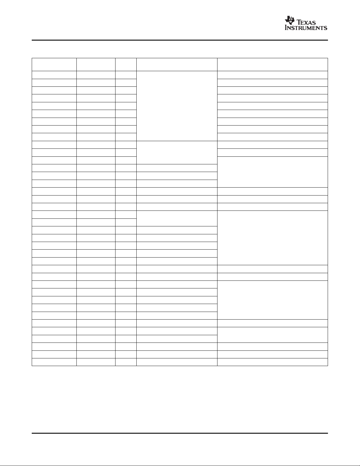
Table 2-1 provides an overview of the TMS320DM6441 SoC. The table shows significant features of the
device, including the capacity of on-chip RAM, peripherals, internal peripheral bus frequency relative to the
C64x+ DSP, and the package type with pin count.
Table 2-1. Characteristics of the Processor
HARDWARE FEATURES DM6441
DDR2 Memory Controller DDR2 (16/32-bit bus width)
Asynchronous EMIF (EMIFA)
Flash Cards
EDMA
Peripherals
Not all peripherals pins
are available at the
same time (For more
detail, see the Device
Configuration section).
On-Chip Memory
CPU ID + CPU Rev ID Control Status Register (CSR.[31:16]) 0x1000
JTAG BSDL_ID 0x0B70 002F
CPU Frequency MHz
Cycle Time ns
Timers separate 32-bit timers)
UART 3 (one with RTS and CTS flow control)
SPI 1 (supports 2 slave devices)
I2C 1 (master/slave)
Audio Serial Port [ASP] 1
10/100 Ethernet MAC with Management Data Input/Output 1
VLYNQ 1
HPI 1 (16-bit multiplexed address/data)
General-Purpose Input/Output Port Up to 71
PWM 3 outputs
ATA/CF 1 (ATA/ATAPI-5)
Configurable Video Ports
USB 2.0 High speed client
Size (Bytes) 160KB RAM, 8KB ROM
Organization
JTAGID register
(address location: 0x01C4 0028)
Asynchronous (8/16-bit bus width) RAM, Flash
Compact Flash
MMC/SD with secure data input/output (SDIO)
SmartMedia/xD
Memory Stick/Memory Stick Pro
64 independent channels
8 QDMA channels
2 64-bit general purpose (each configurable as 2
64-bit watch dog
1 input (VPFE)
1 output (VPBE)
DSP
• 32KB L1 program (L1P)/cache (up to 32KB)
• 80KB L1 data (L1D)/cache (up to 32KB)
• 64KB unified mapped RAM/cache (L2)
ARM
• 16KB I-cache
• 8KB D-cache
• 16KB RAM
• 8KB ROM
DSP 405 MHz , ARM 202.5 MHz at 1.05 V
DSP 513 MHz, ARM 256 MHz at 1.2 V
DSP 2.47 ns, ARM 4.94 ns at 1.05 V
DSP 1.9 ns, ARM 3.9 ns at 1.2V
TMS320DM6441
(NOR, NAND)
Submit Documentation Feedback Device Overview 7
www.ti.com
TMS320DM6441
Digital Media System-on-Chip
SPRS359B – SEPTEMBER 2006 – REVISED JANUARY 2007
Table 2-1. Characteristics of the Processor (continued)
HARDWARE FEATURES DM6441
Voltage
PLL Options x1 (bypass), x15 (1.05 V), x19 (1.2 V)
BGA Package 16 x 16 mm 361-pin BGA (ZWT)
Process Technology µm 0.09 µm
Product Status
(1) PRODUCTION DATA information is current as of publication date. Products conform to specifications per the terms of the Texas
Instruments standard warranty. Production processing does not necessarily include testing of all parameters.
(1)
2.2 Device Compatibility
The ARM926EJ-S RISC CPU is compatible with other ARM9 CPUs from ARM Holdings plc.
The C64x+ DSP core is code-compatible with the C6000™ DSP platform and supports features of the
C64x DSP family.
2.3 ARM Subsystem
Core (V) 1.05 V, 1.2 V
I/O (V) 1.8 V, 3.3 V, 1.2 V
CLKIN frequency multiplier
(27 MHz reference)
Product Preview (PP),
Advance Information (AI), PD
Production Data (PD)
The ARM subsystem is designed to give the ARM926EJ-S (ARM9) master control of the device. In
general, the ARM is responsible for configuration and control of the device; including the DSP subsystem,
the VPSS subsystem, and a majority of the peripherals and external memories.
The ARM subsystem includes the following features:
• ARM926EJ-S RISC processor
• ARMv5TEJ (32/16-bit) instruction set
• Little endian
• Coprocessor 15 (CP15)
• MMU
• 16KB instruction cache
• 8KB data cache
• Write buffer
• 16KB internal RAM (32-bit wide access)
• 8KB internal ROM (ARM bootloader for non-EMIFA boot options)
• Embedded trace module and embedded trace buffer (ETM/ETB)
• ARM interrupt controller
• PLL controller
• Power and sleep controller (PSC)
• System module
2.3.1 ARM926EJ-S RISC CPU
The ARM subsystem integrates the ARM926EJ-S processor. The ARM926EJ-S processor is a member of
ARM9 family of general-purpose microprocessors. This processor is targeted at multi-tasking applications
where full memory management, high performance, low die size, and low power are all important. The
ARM926EJ-S processor supports the 32-bit ARM and 16-bit THUMB instruction sets, enabling the user to
trade off between high performance and high code density. Specifically, the ARM926EJ-S processor
supports the ARMv5TEJ instruction set, which includes features for efficient execution of Java byte codes,
providing Java performance similar to Just in Time (JIT) Java interpreter, but without associated code
overhead.
Device Overview8 Submit Documentation Feedback

www.ti.com
2.3.2 CP15
TMS320DM6441
Digital Media System-on-Chip
SPRS359B – SEPTEMBER 2006 – REVISED JANUARY 2007
The ARM926EJ-S processor supports the ARM debug architecture and includes logic to assist in both
hardware and software debug. The ARM926EJ-S processor has a Harvard architecture and provides a
complete high performance subsystem, including:
• ARM926EJ -S integer core
• CP15 system control coprocessor
• Memory management unit (MMU)
• Separate instruction and data caches
• Write buffer
• Separate instruction and data tightly-coupled memories (TCMs) [internal RAM] interfaces
• Separate instruction and data AHB bus interfaces
• Embedded trace module and embedded trace buffer (ETM/ETB)
For more complete details on the ARM9, refer to the ARM926EJ-S Technical Reference Manual, available
at http://www.arm.com
The ARM926EJ-S system control coprocessor (CP15) is used to configure and control instruction and
data caches, tightly-coupled memories (TCMs), memory management unit (MMU), and other ARM
subsystem functions. The CP15 registers are programmed using the MRC and MCR ARM instructions,
when the ARM in a privileged mode such as supervisor or system mode.
2.3.3 MMU
The ARM926EJ-S MMU provides virtual memory features required by operating systems such as Linux™,
WindowCE®, Ultron®, ThreadX®, etc. A single set of two level page tables stored in main memory is used
to control the address translation, permission checks and memory region attributes for both data and
instruction accesses. The MMU uses a single unified translation lookaside buffer (TLB) to cache the
information held in the page tables. The MMU features are:
• Standard ARM architecture v4 and v5 MMU mapping sizes, domains and access protection scheme.
• Mapping sizes are:
– 1MB (sections)
– 64KB (large pages)
– 4KB (small pages)
– 1KB (tiny pages)
• Access permissions for large pages and small pages can be specified separately for each quarter of
the page (subpage permissions)
• Hardware page table walks
• Invalidate entire TLB, using CP15 register 8
• Invalidate TLB entry, selected by MVA, using CP15 register 8
• Lockdown of TLB entries, using CP15 register 10
2.3.4 Caches and Write Buffer
The size of the instruction cache is 16KB, data cache is 8KB. Additionally, the caches have the following
features:
• Virtual index, virtual tag, and addressed using the modified virtual address (MVA)
• Four-way set associative, with a cache line length of eight words per line (32-bytes per line) and with
two dirty bits in the Dcache
• Dcache supports write-through and write-back (or copy back) cache operation, selected by memory
region using the C and B bits in the MMU translation tables.
• Critical-word first cache refilling
• Cache lockdown registers enable control over which cache ways are used for allocation on a line fill,
Submit Documentation Feedback Device Overview 9

www.ti.com
TMS320DM6441
Digital Media System-on-Chip
SPRS359B – SEPTEMBER 2006 – REVISED JANUARY 2007
providing a mechanism for both lockdown, and controlling cache corruption
• Dcache stores the physical address TAG (PA TAG) corresponding to each Dcache entry in the TAG
RAM for use during the cache line write-backs, in addition to the virtual address TAG stored in the
TAG RAM. This means that the MMU is not involved in Dcache write-back operations, removing the
possibility of TLB misses related to the write-back address.
• Cache maintenance operations provide efficient invalidation of, the entire Dcache or Icache, regions of
the Dcache or Icache, and regions of virtual memory.
The write buffer is used for all writes to a noncachable bufferable region, write-through region and write
misses to a write-back region. A separate buffer is incorporated in the Dcache for holding write-back for
cache line evictions or cleaning of dirty cache lines. The main write buffer has 16-word data buffer and a
four-address buffer. The Dcache write-back has eight data word entries and a single address entry.
2.3.5 Tightly Coupled Memory (TCM)
ARM internal RAM is provided for storing real-time and performance-critical code/data and the interrupt
vector table. ARM internal ROM enables non-EMIFA boot options, such as NAND and UART. The RAM
and ROM memories interfaced to the ARM926EJ-S via the tightly coupled memory interface that provides
for separate instruction and data bus connections. Since the ARM TCM does not allow instructions on the
D-TCM bus or data on the I-TCM bus, an arbiter is included so that both data and instructions can be
stored in the internal RAM/ROM. The arbiter also allows accesses to the RAM/ROM from extra-ARM
sources (e.g., EDMA or other masters). The ARM926EJ-S has built-in DMA support for direct accesses to
the ARM internal memory from a non-ARM master. Because of the time-critical nature of the TCM link to
the ARM internal memory, all accesses from non-ARM devices are treated as DMA transfers.
Instruction and data accesses are differentiated via accessing different memory map regions, with the
instruction region from 0x0000 through 0x7FFF and data from 0x8000 through 0xFFFF. The instruction
region at 0x0000 and data region at 0x8000 map to the same physical 16K-byte TCM RAM. Placing the
instruction region at 0x0000 is necessary to allow the ARM interrupt vector table to be placed at 0x0000,
as required by the ARM architecture. The internal 16K-byte RAM is split into two physical banks of 8KB
each, which allows simultaneous instruction and data accesses to be accomplished if the code and data
are in separate banks.
2.3.6 Advanced High-performance Bus (AHB)
The ARM subsystem uses the AHB port of the ARM926EJ-S to connect the ARM to the config bus and
the external memories. Arbiters are employed to arbitrate access to the separate D-AHB and I-AHB by the
config bus and the external memories bus.
2.3.7 Embedded Trace Macrocell (ETM) and Embedded Trace Buffer (ETB)
To support real-time trace, the ARM926EJ-S processor provides an interface to enable connection of an
embedded trace macrocell (ETM). The ARM926ES-J subsystem in the DM6441 also includes the
embedded trace buffer (ETB). The ETM consists of two parts:
• Trace port provides real-time trace capability for the ARM9.
• Triggering facilities provide trigger resources, which include address and data comparators, counter,
and sequencers.
The DM6441 trace port is not pinned out and is instead only connected to the embedded trace buffer. The
ETB has a 4K-byte buffer memory. ETB enabled debug tools are required to read/interpret the captured
trace data.
2.3.8 ARM Memory Mapping
The ARM memory map is shown in Section 2.5 , Memory Map Summary, of this document. The ARM has
access to memories shown in the following sections.
Device Overview10 Submit Documentation Feedback

www.ti.com
2.3.8.1 ARM Internal Memories
The ARM has access to the following ARM internal memories:
• 16KB ARM internal RAM on TCM interface, logically separated into two 8-KB pages to allow
simultaneous access on any given cycle if there are separate accesses for code (I-TCM bus) and data
(D-TCM) to the different memory regions.
• 8KB ARM internal ROM
2.3.8.2 External Memories
The ARM has access to the following external memories:
• DDR2 synchronous DRAM
• Asynchronous EMIF / NOR flash / NAND flash
• ATA/CF
• Flash card devices:
– MMC/SD with SDIO
– Memory Stick/Memory Stick PRO
– xD
– SmartMedia
2.3.8.3 DSP Memories
TMS320DM6441
Digital Media System-on-Chip
SPRS359B – SEPTEMBER 2006 – REVISED JANUARY 2007
The ARM has access to the following DSP memories:
• L2 RAM
• L1P RAM
• L1D RAM
2.3.8.4 VICP Registers and Memories
The ARM has access to the registers and memories of the video/imaging coprocessor (VICP) subsystem.
2.3.8.5 ARM-DSP Integration
DM6441 ARM and DSP integration features are as follows:
• DSP visibility from ARM’s memory map, see Section 2.5 , Memory Map Summary, for details
• Boot modes for DSP - see Device Configurations section, Section 3.3.3 , DSP Boot, for details
• ARM control of DSP boot / reset - see Device Configurations section, Section 3.3.2 , ARM Boot, for
details
• ARM control of DSP isolation and powerdown / powerup - see Section 3 , Device Configurations, for
details
• ARM & DSP Interrupts - see Section 5.7.1 , ARM CPU Interrupts, and Section 5.7.2 , DSP Interrupts, for
details
2.3.9 Peripherals
The ARM9 has access to all of the peripherals on the DM6441 device with the exception of the VICP.
2.3.10 PLL Controller (PLLC)
The ARM subsystem includes the PLL controller. The PLL controller contains a set of registers for
configuring DM6441’s two internal PLLs (PLL1 and PLL2). The PLL controller provides the following
configuration and control:
• PLL bypass mode
• Set PLL multiplier parameters
• Set PLL divider parameters
• PLL power down
• Oscillator power down
Submit Documentation Feedback Device Overview 11

www.ti.com
TMS320DM6441
Digital Media System-on-Chip
SPRS359B – SEPTEMBER 2006 – REVISED JANUARY 2007
The PLLs are briefly described in this document in Section 5.6 , Clock PLLs. For more detailed information
on the PLLs and PLL Controller register descriptions, see Section 2.8.3 , Documentation Support, of this
document for the TMS320DM644x ARM Subsystem Reference Guide (literature number SPRUE14 ).
2.3.11 Power and Sleep Controller (PSC)
The ARM subsystem includes the power and sleep controller (PSC). Through register settings accessible
by the ARM9, the PSC provides two levels of power savings: peripheral/module clock gating and power
domain shut-off. Brief details on the PSC are given in Section 5.3 , Power Supplies. For more detailed
information and complete register descriptions for the PSC, see Section 2.8.3 , Documentation Support, for
the TMS320DM644x ARM Subsystem Reference Guide (literature number SPRUE14 ).
2.3.12 ARM Interrupt Controller (AINTC)
The ARM interrupt controller (AINTC) accepts device interrupts and maps them to either the ARM’s IRQ
(interrupt request) or FIQ (fast interrupt request). The ARM interrupt controller is briefly described in this
document in the Interrupts section. For detailed information on the ARM interrupt controller, see
Section 2.8.3 , Documentation Support, for the ARM subsystem guide.
2.3.13 System Module
The ARM subsystem includes the system module. The system module consists of a set of registers for
configuring and controlling a variety of system functions. For details and register descriptions for the
system module, see Section 3 , Device Configurations, and see Section 2.8.3 , Documentation Support, for
the TMS320DM644x ARM Subsystem Reference Guide (literature number SPRUE14 ).
2.3.14 Power Management
DM6441 has several means of managing power consumption. There is extensive use of clock gating,
which reduces the power used by global device clocks and individual peripheral clocks. Clock
management can be utilized to reduce clock frequencies in order to reduce switching power. For more
details on power management techniques, see Section 3 , Device Configurations, Section 5 , Peripheral
and Electrical Specifications, and see Section 2.8.3 , Documentation Support, for the TMS320DM644x
ARM Subsystem Reference Guide (literature number SPRUE14 ).
2.4 DSP Subsystem
The DSP subsystem includes the following features:
• C64x+ DSP CPU
• 32KB L1 program (L1P)/cache (up to 32KB)
• 80KB L1 data (L1D)/cache (up to 32KB)
• 64KB unified mapped RAM/cache (L2)
• Little endian
2.4.1 C64x+ DSP CPU Description
The C64x+ central processing unit (CPU) consists of eight functional units, two register files, and two data
paths as shown in Figure 2-1 . The two general-purpose register files (A and B) each contain 32 32-bit
registers for a total of 64 registers. The general-purpose registers can be used for data or can be data
address pointers. The data types supported include packed 8-bit data, packed 16-bit data, 32-bit data,
40-bit data, and 64-bit data. Values larger than 32 bits, such as 40-bit-long or 64-bit-long values are stored
in register pairs, with the 32 LSBs of data placed in an even register and the remaining eight or 32 MSBs
in the next upper register (which is always an odd-numbered register).
The eight functional units (.M1, .L1, .D1, .S1, .M2, .L2, .D2, and .S2) are each capable of executing one
instruction every clock cycle. The .M functional units perform all multiply operations. The .S and .L units
perform a general set of arithmetic, logical, and branch functions. The .D units primarily load data from
memory to the register file and store results from the register file into memory.
Device Overview12 Submit Documentation Feedback

www.ti.com
TMS320DM6441
Digital Media System-on-Chip
SPRS359B – SEPTEMBER 2006 – REVISED JANUARY 2007
The C64x+ CPU extends the performance of the C64x core through enhancements and new features.
Each C64x+ .M unit can perform one of the following each clock cycle: one 32 x 32 bit multiply, one 16 x
32 bit multiply, two 16 x 16 bit multiplies, two 16 x 32 bit multiplies, two 16 x 16 bit multiplies with
add/subtract capabilities, four 8 x 8 bit multiplies, four 8 x 8 bit multiplies with add operations, and four
16 x 16 multiplies with add/subtract capabilities (including a complex multiply). There is also support for
Galois field multiplication for 8-bit and 32-bit data. Many communications algorithms such as FFTs and
modems require complex multiplication. The complex multiply (CMPY) instruction takes four 16-bit inputs
and produces a 32-bit real and a 32-bit imaginary output. There are also complex multiplies with rounding
capability that produces one 32-bit packed output that contain 16-bit real and 16-bit imaginary values. The
32 x 32 bit multiply instructions provide the extended precision necessary for audio and other
high-precision algorithms on a variety of signed and unsigned 32-bit data types.
The .L or (Arithmetic Logic Unit) now incorporates the ability to do parallel add/subtract operations on a
pair of common inputs. Versions of this instruction exist to work on 32-bit data or on pairs of 16-bit data
performing dual 16-bit add and subtracts in parallel. There are also saturated forms of these instructions.
The C64x+ core enhances the .S unit in several ways. In the C64x core, dual 16-bit MIN2 and MAX2
comparisons were only available on the .L units. On the C64x+ core they are also available on the .S unit
which increases the performance of algorithms that do searching and sorting. Finally, to increase data
packing and unpacking throughput, the .S unit allows sustained high performance for the quad 8-bit/16-bit
and dual 16-bit instructions. Unpack instructions prepare 8-bit data for parallel 16-bit operations. Pack
instructions return parallel results to output precision including saturation support.
Other new features include:
• SPLOOP - A small instruction buffer in the CPU that aids in creation of software pipelining loops where
multiple iterations of a loop are executed in parallel. The SPLOOP buffer reduces the code size
associated with software pipelining. Furthermore, loops in the SPLOOP buffer are fully interruptible.
• Compact instructions - The native instruction size for the C6000 devices is 32 bits. Many common
instructions such as MPY, AND, OR, ADD, and SUB can be expressed as 16 bits if the C64x+
compiler can restrict the code to use certain registers in the register file. This compression is
performed by the code generation tools.
• Instruction set enhancement - As noted above, there are new instructions such as 32-bit
multiplications, complex multiplications, packing, sorting, bit manipulation, and 32-bit Galois field
multiplication.
• Exceptions handling - Intended to aid the programmer in isolating bugs. The C64x+ CPU is able to
detect and respond to exceptions, both from internally detected sources (such as illegal op-codes) and
from system events (such as a watchdog time expiration).
• Privilege - Defines user and supervisor modes of operation, allowing the operating system to give a
basic level of protection to sensitive resources. Local memory is divided into multiple pages, each with
read, write, and execute permissions.
• Time-stamp counter - Primarily targeted for real-time operating system (RTOS) robustness, a
free-running time-stamp counter is implemented in the CPU which is not sensitive to system stalls.
For more details on the C64x+ CPU and its enhancements over the C64x architecture, see the following
documents:
• TMS320C64x/C64x+ DSP CPU and Instruction Set Reference Guide (literature number SPRU732 )
• TMS320C64x Technical Overview (literature number SPRU395 )
Submit Documentation Feedback Device Overview 13
www.ti.com
src2
src2
.D1
.M1
.S1
.L1
long src
odd dst
src2
src1
src1
src1
src1
even dst
even dst
odd dst
dst1
dst
src2
src2
src2
long src
DA1
ST1b
LD1b
LD1a
ST1a
Data path A
Odd
register
file A
(A1, A3,
A5...A31)
Odd
register
file B
(B1, B3,
B5...B31)
.D2
src1
dst
src2
DA2
LD2a
LD2b
src2
.M2
src1
dst1
.S2
src1
even dst
long src
odd dst
ST2a
ST2b
long src
.L2
even dst
odd dst
src1
Data path B
Control Register
32 MSB
32 LSB
dst2
(A)
32 MSB
32 LSB
2x
1x
32 LSB
32 MSB
32 LSB
32 MSB
dst2
(B)
(B)
(A)
8
8
8
8
32
32
32
32
(C)
(C)
Even
register
file A
(A0, A2,
A4...A30)
Even
register
file B
(B0, B2,
B4...B30)
(D)
(D)
(D)
(D)
A. On .M unit, dst2 is 32 MSB.
B. On .M unit, dst1 is 32 LSB.
C. On C64x CPU .M unit, src2 is 32 bits; on C64x+ CPU .M unit, src2 is 64 bits.
D. On .L and .S units, odd dst connects to odd register files and even dst connects to even register files.
TMS320DM6441
Digital Media System-on-Chip
SPRS359B – SEPTEMBER 2006 – REVISED JANUARY 2007
Figure 2-1. TMS320C64x+™ CPU (DSP Core) Data Paths
14 Device Overview Submit Documentation Feedback
www.ti.com
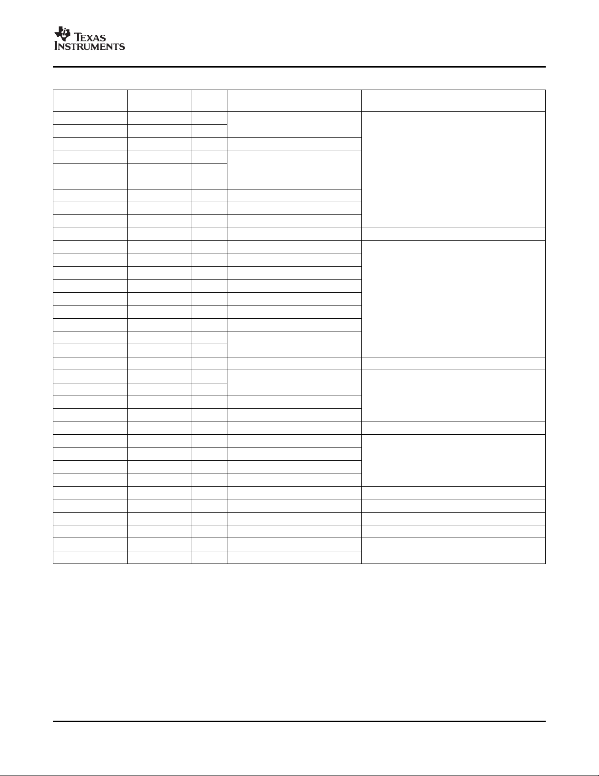
2.4.2 DSP Memory Mapping
The DSP memory map is shown in Table 2-3 . Configuration of the control registers for DDR2, EMIFA, and
ARM internal RAM is supported by the ARM. The DSP has access to memories shown in the following
sections.
2.4.2.1 ARM Internal Memories
The DSP has access to the 16KB ARM internal RAM on the ARM D-TCM interface (i.e., data only).
2.4.2.2 External Memories
The DSP has access to the following external memories:
• DDR2 synchronous DRAM
• Asynchronous EMIF / NOR Flash
2.4.2.3 DSP Internal Memories
The DSP has access to the following DSP memories:
• L2 RAM
• L1P RAM
• L1D RAM
2.4.2.4 C64x+ CPU
TMS320DM6441
Digital Media System-on-Chip
SPRS359B – SEPTEMBER 2006 – REVISED JANUARY 2007
The C64x+ core uses a two-level cache-based architecture. The Level 1 program cache (L1D) is 32 KB
direct mapped cache and the Level 1 data cache (L1D) is 80 KB 2-way set associated cache. The Level 2
memory/cache (L2) consists of a 64 KB memory space that is shared between program and data space.
L2 memory can be configured as mapped memory, cache, or a combination of both.
Table 2-2 shows a memory map of the C64x+ CPU cache registers for the device.
Table 2-2. C64x+ Cache Registers
HEX ADDRESS RANGE REGISTER ACRONYM DESCRIPTION
0x0184 0000 L2CFG L2 cache configuration register
0x0184 0020 L1PCFG L1P size cache configuration register
0x0184 0024 L1PCC L1P freeze mode cache configuration register
0x0184 0040 L1DCFG L1D size cache configuration register
0x0184 0044 L1DCC L1D freeze mode cache configuration register
0x0184 0048 - 0x0184 0FFC - Reserved
0x0184 1000 EDMAWEIGHT L2 EDMA access control register
0x0184 1004 - 0x0184 1FFC - Reserved
0x0184 2000 L2ALLOC0 L2 allocation register 0
0x0184 2004 L2ALLOC1 L2 allocation register 1
0x0184 2008 L2ALLOC2 L2 allocation register 2
0x0184 200C L2ALLOC3 L2 allocation register 3
0x0184 2010 - 0x0184 3FFF - Reserved
0x0184 4000 L2WBAR L2 writeback base address register
0x0184 4004 L2WWC L2 writeback word count register
0x0184 4010 L2WIBAR L2 writeback invalidate base address register
0x0184 4014 L2WIWC L2 writeback invalidate word count register
0x0184 4018 L2IBAR L2 invalidate base address register
0x0184 401C L2IWC L2 invalidate word count register
0x0184 4020 L1PIBAR L1P invalidate base address register
0x0184 4024 L1PIWC L1P invalidate word count register
0x0184 4030 L1DWIBAR L1D writeback invalidate base address register
Submit Documentation Feedback Device Overview 15
www.ti.com
TMS320DM6441
Digital Media System-on-Chip
SPRS359B – SEPTEMBER 2006 – REVISED JANUARY 2007
Table 2-2. C64x+ Cache Registers (continued)
HEX ADDRESS RANGE REGISTER ACRONYM DESCRIPTION
0x0184 4034 L1DWIWC L1D writeback invalidate word count register
0x0184 4038 - Reserved
0x0184 4040 L1DWBAR L1D block writeback
0x0184 4044 L1DWWC L1D block writeback
0x0184 4048 L1DIBAR L1D invalidate base address register
0x0184 404C L1DIWC L1D invalidate word count register
0x0184 4050 - 0x0184 4FFF - Reserved
0x0184 5000 L2WB L2 writeback all register
0x0184 5004 L2WBINV L2 writeback invalidate all register
0x0184 5008 L2INV L2 global invalidate without writeback
0x0184 500C - 0x0184 5027 - Reserved
0x0184 5028 L1PINV L1P global invalidate
0x0184 502C - 0x0184 5039 - Reserved
0x0184 5040 L1DWB L1D global writeback
0x0184 5044 L1DWBINV L1D global writeback with invalidate
0x0184 5048 L1DINV L1D global invalidate without writeback
0x0184 8000 - 0x0184 8004 MAR0 - MAR1 Reserved 0x0000 0000 - 0x01FF FFFF
0x0184 8008 - 0x0184 8024 MAR2 - MAR9 Memory attribute registers for EMIFA 0x0200 0000 - 0x09FF FFFF
0x0184 8028 - 0x0184 802C MAR10 - MAR11 Reserved 0x0A00 0000 - 0x0BFF FFFF
0x0184 8030 - 0x0184 803C MAR12 - MAR15 Memory attribute registers for VLYNQ 0x0C00 0000 - 0x0FFF FFFF
0x0184 8040 - 0x0184 8104 MAR16 - MAR65 Reserved 0x1000 0000 - 0x41FF FFFF
0x0184 8108 - 0x0184 813C MAR66 - MAR79
0x0184 8140- 0x0184 81FC MAR80 - MAR127 Reserved 0x5000 0000 - 0x7FFF FFFF
0x0184 8200 - 0x0184 823C MAR128 - MAR143 Memory attribute registers for DDR2 0x8000 0000 - 0x8FFF FFFF
0x0184 8240 - 0x0184 83FC MAR144 - MAR255 Reserved 0x9000 0000 - 0xFFFF FFFF
Memory attribute registers for EMIFA/VLYNQ shadow 0x4200 0000 0x4FFF FFFF
2.4.3 Peripherals
The DSP has controllability for the following peripherals:
• VICP
• EDMA
• ASP
• Two Timers (Timer 0 and Timer1) that can each be configured as one 64-bit or two 32-bit timers
2.4.4 DSP Interrupt Controller
The DSP interrupt controller accepts device interrupts and appropriately maps them to available DSP
interrupts. The DSP interrupt controller is briefly described in this document in the Interrupts section. For
more detailed on the DSP interrupt controller, see Section 2.8.3 , Documentation Support, of this document
for the C64x+ CPU user's guide.
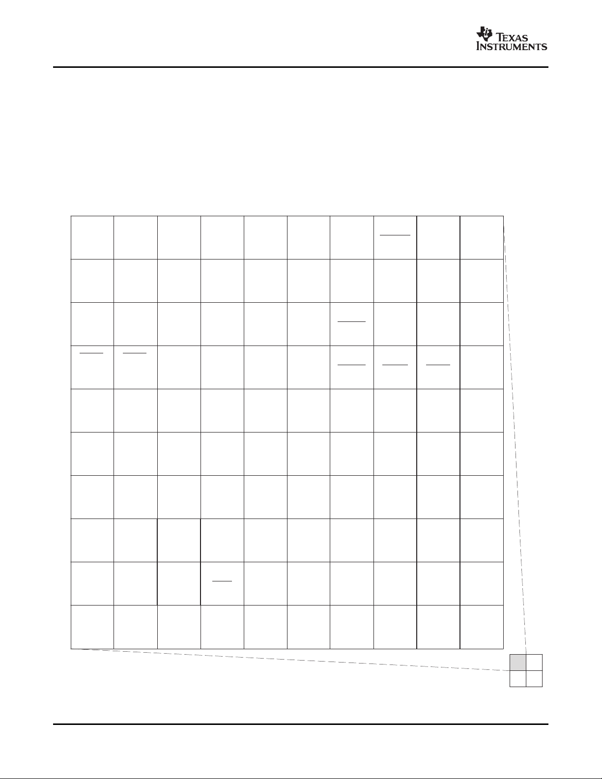
2.5 Memory Map Summary
Table 2-3 shows the memory map address ranges of the device. Table 2-4 depicts the expanded map of
the configuration space (0x0180 0000 through 0x0FFF FFFF). The device has multiple on-chip memories
associated with its two processors and various subsystems. To help simplify software development a
unified memory map is used where possible to maintain a consistent view of device resources across all
bus masters.
Device Overview16 Submit Documentation Feedback
www.ti.com
Table 2-3. Memory Map Summary
TMS320DM6441
Digital Media System-on-Chip
SPRS359B – SEPTEMBER 2006 – REVISED JANUARY 2007
START END SIZE EDMA/
ADDRESS ADDRESS (Bytes) PERIPHERAL
0x0000 0000 0x0000 1FFF 8K ARM RAM0 (Instruction)
0x0000 2000 0x0000 3FFF 8K ARM RAM1 (Instruction)
0x0000 4000 0x0000 5FFF 8K ARM ROM (Instruction)
0x0000 6000 0x0000 7FFF 8K Reserved
0x0000 8000 0x0000 9FFF 8K ARM RAM0 (Data) Reserved ARM RAM0 ARM RAM0
0x0000 A000 0x0000 BFFF 8K ARM RAM1 (Data) ARM RAM1 ARM RAM1
0x0000 C000 0x0000 DFFF 8K ARM ROM (Data) ARM ROM ARM ROM
0x0000 E000 0x0000 FFFF 8K
0x0001 0000 0x000F FFFF 960K
0x0010 0000 0x001F FFFF 1M VICP
0x0020 0000 0x007F FFFF 6M Reserved
0x0080 0000 0x0080 FFFF 64K L2 RAM/Cache
0x0081 0000 0x00E0 7FFF 6112K Reserved
0x00E0 8000 0x00E0 FFFF 32K L1P Cache
0x00E1 0000 0x00F0 3FFF 976K Reserved
0x00F0 4000 0x00F0 FFFF 48K L1D RAM
0x00F1 0000 0x00F1 7FFF 32K L1D Cache
0x00F1 8000 0x017F FFFF 9120K Reserved
0x0180 0000 0x01BB FFFF 3840K
0x01BC 0000 0x01BC 0FFF 4K ARM ETB Memory
0x01BC 1000 0x01BC 17FF 2K ARM ETB Registers CFG Space
0x01BC 1800 0x01BC 18FF 256 ARM IceCrusher
0x01BC 1900 0x01BF FFFF 255744 Reserved
0x01C0 0000 0x01FF FFFF 4M CFG Bus Peripherals CFG Bus Peripherals CFG Bus Peripherals
0x0200 0000 0x09FF FFFF 128M EMIFA (Code and Data) EMIFA (Data) EMIFA (Data) Reserved
0x0A00 0000 0x0BFF FFFF 32M Reserved Reserved
0x0C00 0000 0x0FFF FFFF 64M VLYNQ (Remote) Reserved VLYNQ (Remote)
0x1000 0000 0x1000 7FFF 32K Reserved
0x1000 8000 0x1000 9FFF 8K ARM RAM0 ARM RAM0
0x1000 A000 0x1000 BFFF 8K ARM RAM1 ARM RAM1
0x1000 C000 0x1000 DFFF 8K ARM ROM ARM ROM
0x1000 E000 0x1000 FFFF 8K
0x1001 0000 0x110F FFFF 17344K
0x1110 0000 0x111F FFFF 1M VICP VICP VICP
0x1120 0000 0x117F FFFF 6M Reserved Reserved Reserved
0x1180 0000 0x1180 FFFF 64K L2 RAM/Cache L2 RAM/Cache L2 RAM/Cache
0x1181 0000 0x11E0 7FFF 6112K Reserved Reserved Reserved
0x11E0 8000 0x11E0 FFFF 32K L1P Cache L1P Cache L1P Cache
0x11E1 0000 0x11F0 3FFF 976K Reserved Reserved Reserved
0x11F0 4000 0x11F0 FFFF 48K L1D RAM L1D RAM L1D RAM
0x11F1 0000 0x11F1 7FFF 32K L1D RAM/Cache L1D RAM/Cache L1D RAM/Cache
0x11F1 8000 0x1FFF FFFF 241M-32K Reserved Reserved Reserved
0x2000 0000 0x2000 7FFF 32K DDR2 Control Regs DDR2 Control Regs DDR2 Control Regs DDR2 Control Regs
0x2000 8000 0x41FF FFFF 544M-32k Reserved Reserved Reserved Reserved
0x4200 0000
0x5000 0000 0x7FFF FFFF 768M Reserved Reserved Reserved
0x8000 0000 0x8FFF FFFF 256M DDR2 DDR2 DDR2 DDR2
0x9000 0000 0xFFFF FFFF 1792M Reserved Reserved Reserved Reserved
(1)
0x4FFF FFFF 224M Reserved EMIFA/VLYNQ Shadow EMIFA/VLYNQ Shadow
Reserved
Reserved
ARM C64x+ HPI VPSS
Reserved Reserved
Reserved
Reserved Reserved
(1) EMIFA shadow memory started a 0x4200 0000 is physically the same memory as location 0x0200 0000. Memory range 0x200 0000
through 0x09FF FFFF should only be used by C64x+ for data accesses. Memory range 0x4200 0000 through 0x4FFF FFFF can be
used by C64x+ for both code execution and data accesses.
Reserved
Submit Documentation Feedback Device Overview 17
www.ti.com
TMS320DM6441
Digital Media System-on-Chip
SPRS359B – SEPTEMBER 2006 – REVISED JANUARY 2007
Table 2-4. Configuration Memory Map Summary
START END SIZE ARM/EDMA C64x+
ADDRESS ADDRESS (Bytes)
0x0180 0000 0x0180 FFFF 64K C64x+ interrupt controller
0x0181 0000 0x0181 0FFF 4K C64x+ powerdown controller
0x0181 1000 0x0181 1FFF 4K C64x+ security ID
0x0181 2000 0x0181 2FFF 4K C64x+ revision ID
0x0182 0000 0x0182 FFFF 64K Reserved C64x+ EMC
0x0183 0000 0x0183 FFFF 64K Reserved
0x0184 0000 0x0184 FFFF 64K C64x+ memory system
0x0185 0000 0x0187 FFFF 192K Reserved
0x0188 0000 0x01BB FFFF 3328K Reserved
0x01BC 0000 0x01BC 00FF 256 AET registers
0x01BC 0100 0x01BC 01FF 256 ARM ETB Memory Pin manager and trace
0x01BC 0200 0x01BC 0FFF 3.5K
0x01BC 1000 0x01BC 17FF 2K ARM ETB Registers
0x01BC 1800 0x01BC 18FF 256 ARM Ice Crusher
0x01BC 1900 0x01BF FFFF 255744 Reserved
0x01C0 0000 0x01C0 FFFF 64K EDMA CC EDMA CC
0x01C1 0000 0x01C1 03FF 1K EDMA TC0 EDMA TC0
0x01C1 0400 0x01C1 07FF 1K EDMA TC1 EDMA TC1
0x01C1 8800 0x01C1 9FFF 6K
0x01C1 A000 0x01C1 FFFF 24K
0x01C2 0000 0x01C2 03FF 1K UART0
0x01C2 0400 0x01C2 07FF 1K UART1 Reserved
0x01C2 0800 0x01C2 0BFF 1K UART2
0x01C2 0C00 0x01C2 0FFF 1K Reserved
0x01C2 1000 0x01C2 13FF 1K I2C
0x01C2 1400 0x01C2 17FF 1K Timer0 Timer0
0x01C2 1800 0x01C2 1BFF 1K Timer1 Timer1
0x01C2 1C00 0x01C2 1FFF 1K Timer2 (WatchDog)
0x01C2 2000 0x01C2 23FF 1K PWM0
0x01C2 2400 0x01C2 27FF 1K PWM1 Reserved
0x01C2 2800 0x01C2 2BFF 1K PWM2
0x01C2 2C00 0x01C3 FFFF 117K Reserved
0x01C4 0000 0x01C4 07FF 2K System Module System module
0x01C4 0800 0x01C4 0BFF 1K PLL Controller 1
0x01C4 0C00 0x01C4 0FFF 1K PLL Controller 2
0x01C4 1000 0x01C4 1FFF 4K Power and Sleep Controller Power and sleep controller
0x01C4 2000 0x01C4 202F 48 Reserved Reserved
0x01C4 2030 0x01C4 2033 4 DDR2 VTP Reg DDR2 VTP reg
Reserved
Reserved
Reserved
Device Overview18 Submit Documentation Feedback
www.ti.com
SPRS359B – SEPTEMBER 2006 – REVISED JANUARY 2007
Table 2-4. Configuration Memory Map Summary (continued)
START END SIZE ARM/EDMA C64x+
ADDRESS ADDRESS (Bytes)
0x01C4 2034 0x01C4 23FF 1K - 52
0x01C4 2400 0x01C4 7FFF 23K
0x01C4 8000 0x01C4 83FF 1K ARM interrupt controller
0x01C4 8400 0x01C5 FFFF 95K
0x01C6 0000 0x01C6 3FFF 16K Reserved
0x01C6 4000 0x01C6 5FFF 8K USB2.0 Regs / RAM
0x01C6 6000 0x01C6 67FF 2K ATA/CF
0x01C6 6800 0x01C6 6FFF 2K SPI
0x01C6 7000 0x01C6 77FF 2K GPIO
0x01C6 7800 0x01C6 7FFF 2K HPI HPI
0x01C6 8000 0x01C6 FFFF 32K Reserved
0x01C7 0000 0x01C7 3FFF 16K VPSS Regs
0x01C7 4000 0x01C7 FFFF 48K Reserved
0x01C8 0000 0x01C8 0FFF 4K EMAC Control Regs
0x01C8 1000 0x01C8 1FFF 4K EMAC Control Module Regs Reserved
0x01C8 2000 0x01C8 3FFF 8K EMAC Control Module RAM
0x01C8 4000 0x01C8 47FF 2K MDIO Control Regs
0x01C8 4800 0x01C8 4FFF 2K
0x01C8 5000 0x01CB FFFF 236K
0x01CC 0000 0x01CD FFFF 128K VICP VICP
0x01CE 0000 0x01CF FFFF 128K
0x01D0 0000 0x01DF FFFF 1M
0x01E0 0000 0x01E0 0FFF 4K EMIFA Control
0x01E0 1000 0x01E0 1FFF 4K VLYNQ Control Regs
0x01E0 2000 0x01E0 3FFF 8K ASP ASP
0x01E0 4000 0x01E0 FFFF 48K Reserved
0x01E1 0000 0x01E1 FFFF 64K MMC/SD/SDIO
0x01E2 0000 0x01E3 FFFF 128K Memory Stick/Memory Stick Pro
0x01E4 0000 0x01FF FFFF 1792K Reserved
0x0200 0000 0x03FF FFFF 32M EMIFA Data/Code (CS2) EMIFA data (CS2)
0x0400 0000 0x05FF FFFF 32M EMIFA Data/Code (CS3) EMIFA data (CS3)
0x0600 0000 0x07FF FFFF 32M EMIFA Data/Code (CS4) EMIFA data (CS4)
0x0800 0000 0x09FF FFFF 32M EMIFA Data/Code (CS5) EMIFA data (CS5)
0x0A00 0000 0x0BFF FFFF 32M Reserved
0x0C00 0000 0x0FFF FFFF 64M VLYNQ (Remote)
Reserved
Reserved
Reserved
Reserved
Reserved
Reserved
Reserved
TMS320DM6441
Digital Media System-on-Chip
Submit Documentation Feedback Device Overview 19
www.ti.com
W
V
U
T
R
P
N
M
L
K
10987654321
10987654321
DDR_D[1]
DV
DDR2
EM_A[4]/
GPIO27
CLK_OUT0/
GPIO48
MXI/CLKIN
EM_A[5]/
GPIO26
MXV
SS
PLLV
DD18
RSV24
EM_A[6]/
GPIO25
EM_A[8]/
GPIO23
EM_A[7]/
GPIO24
EM_A[13]/
GPIO18
EM_A[10]/
GPIO21
EM_A[15]/
GPIO16/
VLYNQ_TXD3
EM_A[11]/
GPIO20
EM_A[17]/
GPIO14/
VLYNQ_TXD2
EM_A[19]/
GPIO12/
VLYNQ_TXD1
EM_A[20]/
GPIO11/
VLYNQ_RXD0
EM_CS4/
GPIO9/
VLYNQ_
SCRUN
DDR_
DQM[0]
DDR_D[0]
EM_A[21]/
GPIO10/
VLYNQ_TXD0
EM_A[14]/
GPIO17/
VLYNQ_RXD3
EM_A[9]/
GPIO22
MXV
DD
RESET
V
SS
RSV3
V
SS
CV
DD
DV
DDR2
DV
DDR2
V
SS
V
SS
DDR_A[11]DDR_A[12]DDR_CLK0DDR_CLK0DDR_D[14]
DV
DDR2
V
SS
V
SS
DDR_D[5]
DDR_D[6]
DDR_D[9]
DV
DD18
EM_A[16]/
GPIO15/
VLYNQ_RXD2
DV
DDR2
DDR_BS[2]
CV
DD
DDR_D[11] DDR_D[15] DDR_CKE DDR_A[8]
V
SS
DV
DDR2
V
SS
V
SS
DV
DDR2
DDR_
DQM[1]
DDR_CAS DDR_WE DDR_VDDDLL
CV
DDDSP
CV
DD
DDR_DQS[1] DDR_RAS DDR_A[10]
CV
DD
CV
DD
DDR_D[2] DDR_D[3] DDR_D[8] DDR_D[13] DDR_BS[1]
DDR_D[4] DDR_D[12]
V
SS
EM_A[3]/
GPIO28
DV
DD18
CV
DD
DV
DD18
RSV7
MXO V
SS
DV
DD18
V
SS
EM_A[18]/
GPIO13/
VLYNQ_RXD1
V
SS
EM_A[12]/
GPIO19
V
SS
DDR_CS
CV
DDDSP
DDR_DQS[0] DDR_D[10] DDR_BS[0]
EM_CS5/
GPIO8/
VLYNQ_
CLOCK
RSV6
DDR_D[7]
W
V
U
T
R
P
N
M
L
K
TMS320DM6441
Digital Media System-on-Chip
SPRS359B – SEPTEMBER 2006 – REVISED JANUARY 2007
2.6 Pin Assignments
Extensive use of pin multiplexing is used to accommodate the largest number of peripheral functions in
the smallest possible package. Pin multiplexing is controlled using a combination of hardware
configuration at device reset and software programmable register settings. For more information on pin
muxing, see Section 3.5.2 , Multiplexed Pin Configurations, of this document.
2.6.1 Pin Map (Bottom View)
Figure 2-2 through Figure 2-5 show the bottom view of the package pin assignments in four quadrants (A,
B, C, and D).
Device Overview20 Submit Documentation Feedback
Figure 2-2. Pin Map [Quadrant A]
www.ti.com
W
V
U
T
R
P
N
M
L
K
191817161514131211
191817161514131211
DDR_A[9]
V
SS
V
SS
CV
DD
CV
DD
V
SS
CV
DD
V
SS
DV
DDR2
DV
DDR2
DV
DDR2
V
SS
DV
DDR2
DV
DDR2
V
SS
DDR_
VSSDLL
DDR_ZPDDR_ZN
V
SS
V
SS
V
SS
DV
DD18
DV
DD18
HD PCLK
V
DDA_1P8V
CI6/CCD14/
UART_TXD2
CI7/CCD15/
UART_RXD2
DAC_IOUT_B
RSV4DDR_D[29]DDR_D[27]DDR_D[21]DDR_D[18]
DAC_IOUT_A
YI4/CCD4
DAC_RBIAS
DDR_A[3]
DDR_A[4]
DDR_A[0]
V
SS
V
SS
DDR_DQM[2]
DDR_D[26]
YI7/CCD7
DDR_D[17] DDR_D[22] DDR_D[24] DDR_D[30]
YI0/CCD0
V
SSA_1P8V
CI5/CCD13/
UART_CTS2
CI1/CCD9
CI4/CCD12/
UART_RTS2
DDR_VREF DDR_DQM[3] DDR_D[23] DAC_IOUT_D
YI1/CCD1 YI3/CCD3
DDR_D[20] DDR_DQS[3] DDR_D[31]
YI6/CCD6 VD
DDR_A[7] DDR_A[2] DDR_D[19] DDR_D[28]
DDR_A[6] DDR_D[16]
DAC_IOUT_C
CV
DDDSP
V
SS
CI2/CCD10
YI5/CCD5
DAC_V
REF
DV
DD18
CI0/CCD8
CI3/CCD11
DV
DDR2
V
DDA_1P1V
DV
DDR2
V
SSA_1P1V
YI2/CCD2
DDR_A[1] DDR_DQS[2] DDR_D[25]
V
SS
DDR_A[5]
W
V
U
T
R
P
N
M
L
K
TMS320DM6441
Digital Media System-on-Chip
SPRS359B – SEPTEMBER 2006 – REVISED JANUARY 2007
Figure 2-3. Pin Map [Quadrant B]
Submit Documentation Feedback Device Overview 21
www.ti.com
H
G
F
E
D
C
B
A
191817161514131211
191817161514131211
CV
DDDSP
YOUT4/R4/
AEAW4
GPIOV33_1/
TXCLK
GPIOV33_2/
COL
GPIOV33_9/
RXD2
GPIOV33_8/
RXD1
GPIOV33_6/
TXD3
GPIOV33_4/
TXD1
GPIOV33_12/
RXDV
GPIO2/G0
GPIOV33_7/
RXD0
GPIOV33_10/
RXD3
DV
DD33
DV
DD33
DV
DD33
V
SS
V
SS
V
SS
GPIO1/
C_WE
GPIO0/
LCD_OE
GPIO4/R0/
C_FIELD
GPIOV33_0/
TXEN
GPIO6/B1
VSYNC VPBECLK
M24XI
YOUT3/R3/
AEAW3
VCLK
YOUT7/R7
CLK_OUT1/
TIM_IN/
GPIO49
PWM1/R2/
GPIO46
M24V
DD
CV
DDDSP
GPIO38/R1
DV
DD18
V
SS
USB_R1
COUT5/G2
COUT0/B3/
BTSEL0
YOUT6/R6
YOUT2/G7/
AEAW2
COUT7/G4
YOUT1/G6/
AEAW1
DV
DD18
USB_
V
SSREF
USB_
V
SSA1P2LD0
USB_DP
COUT2/B5/
EM_WIDTH
RSV2
V
SS
USB_V
SS1P8
USB_DM
COUT3/B6/
DSP_BT
COUT6/G3
M24XO
GPIOV33_5/
TXD2
PWM2/
B2/GPIO47
HSYNC
COUT1/B4/
BTSEL1
M24V
SS
GPIO3/B0/
LCD_FIELD
PWM0/
GPIO45
YOUT0/G5/
AEAW0
GPIO5/G1 YOUT5/R5
CV
DD
USB_
V
DDA1P2LD0
COUT4/B7
V
SS
DV
DD18
USB_V
DD1P8
GPIOV33_3/
TXD0
H
G
F
E
D
C
B
A
J
CV
DDDSP
V
SS
USB_
V
SSA3P3
DV
DD18
USB_ID
USB_
V
DDA3P3
CV
DDDSP
V
SS
USB_VBUS
J
TMS320DM6441
Digital Media System-on-Chip
SPRS359B – SEPTEMBER 2006 – REVISED JANUARY 2007
Figure 2-4. Pin Map [Quadrant C]
Device Overview22 Submit Documentation Feedback
www.ti.com
J
H
G
F
E
D
C
B
A
10987654321
10987654321
EM_BA[1]/
DA1/
GPIO52
TMS
SPI_EN0/
GPIO37
RSV1
EM_CS3
SPI_CLK/
GPIO39
SPI_EN1/
HDDIR/
GPIO42
EM_CS2/
HCS
GPIO7
EM_D12/
DD12/
HD12
EM_D1/
DD1/
HD1
EM_D5/
DD5/
HD5
RSV5
EM_D15/
DD15/
HD15
EM_D3/
DD3/
HD3
EM_D9/
DD9/
HD9
EM_D13/
DD13/
HD13
EM_D6/
DD6/
HD6
EM_D8/
DD8/
HD8
EM_WE/(WE)/
(IOWR)/DIOW/
HDS2
EM_D11/
DD11/
HD11
GPIO51/
ATA_CS1
EM_R/W/
INTRQ/
HR/W
EM_D4/
DD4/
HD4
SCL/
GPIO43
TDOSDA/GPIO44
TDI
SD_DATA3
GPIOV33_14/
CRS
V
SS
SD_DATA2
GPIOV33_13/
RXER
SD_DATA1
GPIOV33_15/
MDIO
RTCK
V
SS
DMACK/
UART_TXD1
EM_BA[0]/
DA0/
HINT
UART_RXD0/
GPIO35
EM_D2/
DD2/
HD2
EM_D10/
DD10/
HD10
V
SS
SD_CMD
GPIO50/
ATA_CS0
DV
DD18
V
SS
CV
DDDSP
DR/
GPIO34
V
SS
SD_DATA0
FSR/
GPIO32
TRST
V
SS
DV
DD18
V
SS
V
SS
CLKR/
GPIO30
GPIOV33_11/
RXCLK
DV
DD18
V
SS
CV
DDDSP
CLKX/
GPIO29
GPIOV33_16/
MDCLK
EM_A[2]/
(CLE)/
HCNTL0
EM_A[1]/
(ALE)/
HHWIL
EM_A[0]/
DA2/
HCNTL1/
GPIO53
V
SS
CV
DDDSP
DV
DD33
SPI_DO/
GPIO41
TCK
FSX/
GPIO31
DX/
GPIO33
DV
DD18
EM_D7/
DD7/
HD7
UART_TXD0/
GPIO36
EMU1
EMU0
EM_D0/
DD0/
HD0
DV
DD18
EM_WAIT/
(RDY/BSY)/
IORDY/
HRDY
DV
DD18
DV
DD18
SD_CLK
EM_OE/(RE)/
(IORD)/DIOR/
HDS1
EM_D14/
DD14/
HD14
CV
DDDSP
DMARQ/
UART_RXD1
SPI_DI/
GPIO40
J
H
G
F
E
D
C
B
A
TMS320DM6441
Digital Media System-on-Chip
SPRS359B – SEPTEMBER 2006 – REVISED JANUARY 2007
Figure 2-5. Pin Map [Quadrant D]
Submit Documentation Feedback Device Overview 23
www.ti.com
TMS320DM6441
Digital Media System-on-Chip
SPRS359B – SEPTEMBER 2006 – REVISED JANUARY 2007
2.7 Terminal Functions
The terminal functions tables (Table 2-5 through Table 2-31 ) identify the external signal names, the
associated pin (ball) numbers along with the mechanical package designator, the pin type, whether the pin
has any internal pullup or pulldown resistors, and a functional pin description. For more detailed
information on device configuration, peripheral selection, multiplexed/shared pin, and debugging
considerations, see Section 3 , Device Configurations, of this data manual.
Table 2-5. BOOT Terminal Functions
SIGNAL
NAME NO.
COUT0/
B3/ A16 I/O/Z
BTSEL0
COUT1/
B4/ B16 I/O/Z 0 1 ARM EMIFA boot (NOR)
BTSEL1
COUT2/
B5/ A17 I/O/Z
EM_WIDTH
COUT3/
B6/ B17 I/O/Z
DSP_BT
YOUT0/
G5/ D15 I/O/Z
AEAW0
YOUT1/
G6/ D16 I/O/Z
AEAW1
YOUT2/ input states of AEAW[4:0] are sampled to set the EMIFA address bus
G7/ D17 I/O/Z width. See Section 3.4.2 , Peripheral Selection at Device Reset, for details.
AEAW2 After reset, these are video encoder outputs YOUT[0:4] or RGB666/888
YOUT3/
R3/ D18 I/O/Z
AEAW3
YOUT4/
R4/ E15 I/O/Z
AEAW4
(1) I = Input, O = Output, Z = High impedance, S = Supply voltage, GND = Ground, A = Analog signal
(2) IPD = internal pulldown, IPU = internal pullup. (To pull up a signal to the opposite supply rail, a 1-k Ω resistor should be used.)
(3) Specifies the operating I/O supply voltage for each signal
(1)
TYPE
(2) (3)
OTHER
BOOT
These pins are multiplexed between ARM boot mode and the VPBE. At
IPD determine the ARM boot configuration. See below for the boot modes set
DV
DD18
IPD
DV
DD18
IPD 8-bit wide EMIFA data bus, EM_WIDTH = 0. For a 16-bit wide EMIFA data
DV
DD18
IPD booted by the ARM when DSP_BT=0. The DSP boots from EMIFA when
DV
DD18
IPD
DV
DD18
IPD
DV
DD18
IPD
DV
DD18
IPD
DV
DD18
IPD
DV
DD18
reset, the boot mode inputs BTSEL0 and BTSEL1 are sampled to
by these inputs. See Section 3.3 , Bootmode for more details.
After reset, these are video encoder outputs COUT0 and COUT1, or
RGB666/888 Blue output data bits 3 and 4 B3/B4.
BTSEL1 BTSEL0 ARM Boot Mode
0 0 ARM ROM boot (NAND) [default]
1 0 ARM ROM boot (HPI)
1 1 ARM ROM boot (UART0)
This pin is multiplexed between EMIFA and the VPBE. At reset, the input
state is sampled to set the EMIFA data bus width (EM_WIDTH). For an
bus, EM_WIDTH = 1.
After reset, it is video encoder output COUT2 or RGB666/888 Blue output
data bit 5 B5.
This pin is multiplexed between DSP boot and the VPBE. At reset, the
input state is sampled to set the DSP boot source DSP_BT. The DSP is
DSP_BT=1.
After reset, it is video encoder output COUT3 or RGB666/888 Blue data
bit 6 output B6.
These pins are multiplexed between EMIFA and the VPBE. At reset, the
Red and Green data bit outputs G5, G6, G7, R3, and R4.
DESCRIPTION
24 Device Overview Submit Documentation Feedback
www.ti.com
Table 2-6. Oscillator/PLL Terminal Functions
TMS320DM6441
Digital Media System-on-Chip
SPRS359B – SEPTEMBER 2006 – REVISED JANUARY 2007
SIGNAL
NAME NO.
(1)
TYPE
(2)
OTHER
DESCRIPTION
OSCILLATOR, PLL
MXI/ Crystal input MXI for MX oscillator (system oscillator, typically 27 MHz).
CLKIN If the internal oscillator is bypassed, this is the external oscillator clock input.
MXO M1 O DV
MXV
DD
MXV
SS
M24XI F18 I DV
M24XO F19 O DV
M24V
DD
M24V
SS
PLLV
DD18
APLLREFV M3 S
L1 I DV
L5 S
L2 GND
F16 S
F17 GND
M2 S
DD18
DD18
(3)
(3)
DD18
DD18
(3)
(3)
(3)
(3)
Crystal output for MX oscillator
1.8V power supply for MX oscillator
Ground for MX oscillator
Crystal input for M24 oscillator (24 MHz for USB)
Crystal output for M24 oscillator
1.8V power supply for M24 oscillator
Ground for M24 oscillator
1.8 Volt power supply for PLLs (system and USB)
Core voltage reference for PLL logic
(1) I = Input, O = Output, Z = High impedance, S = Supply voltage, GND = Ground, A = Analog signal
(2) Specifies the operating I/O supply voltage for each signal
(3) For more information, see the Recommended Operating Conditions table
Table 2-7. Clock Generator Terminal Functions
SIGNAL
NAME NO.
CLK_OUT0/
GPIO48
K1 I/O/Z DV
CLK_OUT1/ This pin is multiplexed between the USB clock generator, timer, and GPIO.
TIM_IN/ E19 I/O/Z DV
GPIO49 12 MHz or 24 MHz clock outputs.
(1) I = Input, O = Output, Z = High impedance, S = Supply voltage, GND = Ground, A = Analog signal
(2) Specifies the operating I/O supply voltage for each signal
(1)
TYPE
(2)
OTHER
DESCRIPTION
CLOCK GENERATOR
This pin is multiplexed between the PLL1 clock generator and GPIO.
DD18
DD18
For the PLL1 clock generator, it is clock output CLK_OUT0. This is configurable for
13.5 MHz or 27 MHz clock outputs.
For the USB clock generator, it is clock output CLK_OUT1. This is configurable for
Table 2-8. RESET and JTAG Terminal Functions
SIGNAL
NAME NO.
RESET L4 I This is the active low global reset input.
TMS E6 I JTAG test-port mode select input
TDO B5 O/Z JTAG test-port data output
TDI A5 I JTAG test-port data input
TCK A6 I JTAG test-port clock input
RTCK B6 O/Z JTAG test-port return clock output
(1) I = Input, O = Output, Z = High impedance, S = Supply voltage, GND = Ground, A = Analog signal
(2) IPD = internal pulldown, IPU = internal pullup. (To pull up a signal to the opposite supply rail, a 1-k Ω resistor should be used.)
(3) Specifies the operating I/O supply voltage for each signal
Submit Documentation Feedback Device Overview 25
(1)
TYPE
(2) (3)
OTHER
DESCRIPTION
RESET
IPU
DV
DD18
JTAG
IPU
DV
DD18
–
DV
DD18
IPU
DV
DD18
IPU
DV
DD18
–
DV
DD18
www.ti.com
TMS320DM6441
Digital Media System-on-Chip
SPRS359B – SEPTEMBER 2006 – REVISED JANUARY 2007
Table 2-8. RESET and JTAG Terminal Functions (continued)
SIGNAL
NAME NO.
TRST D7 I
EMU1 C6 I/O/Z Emulation pin 1
EMU0 D6 I/O/Z Emulation pin 0
(1)
TYPE
(2) (3)
OTHER
IPD JTAG test-port reset. For IEEE 1149.1 JTAG compatibility, see the IEEE 1149.1
DV
DD18
IPU
DV
DD18
IPU
DV
DD18
Table 2-9. EMIFA Terminal Functions
DESCRIPTION
JTAG compatibility statement portion of this data manual .
SIGNAL
NAME NO.
(1)
TYPE
(2)
OTHER
DESCRIPTION
EMIFA BOOT CONFIGURATION
This pin is multiplexed between EMIFA and the VPBE. At reset, the input state is
COUT2/ sampled to set the EMIFA data bus width (EM_WIDTH). For an 8-bit wide EMIFA
B5/ A17 I/O/Z DV
EM_WIDTH After reset, it is video encoder output COUT2 or RGB666/888 Blue output data bit 5
DD18
data bus, EM_WIDTH = 0. For a 16-bit wide EMIFA data bus, EM_WIDTH = 1.
B5.
This pin is multiplexed between DSP boot and the VPBE. At reset, the input state is
COUT3/ sampled to set the DSP boot source DSP_BT. The DSP is booted by the ARM when
B6/ B17 I/O/Z DV
DSP_BT After reset, it is video encoder output COUT3 or RGB666/888 Blue data bit 6 output
DD18
DSP_BT=0. The DSP boots from EMIFA when DSP_BT=1.
B6.
YOUT0/
G5/ D15 I/O/Z DV
AEAW0
DD18
YOUT1/
G6/ D16 I/O/Z DV
AEAW1
DD18
These pins are multiplexed between EMIFA and the VPBE. At reset, the input states
YOUT2/ of AEAW[4:0] are sampled to set the EMIFA address bus width. See Section 3.4.2 ,
G7/ D17 I/O/Z DV
AEAW2 After reset, these are video encoder outputs YOUT[0:4] or RGB666/888 Red and
DD18
YOUT3/
R3/ D18 I/O/Z DV
AEAW3
DD18
Peripheral Selection at Device Reset for details.
Green data bit outputs G5, G6, G7, R3, and R4.
YOUT4/
R4/ E15 I/O/Z DV
AEAW4
DD18
EMIFA FUNCTIONAL PINS: ASYNC / NOR
For EMIFA, this pin is Chip Select 2 output EM_CS2 for use with asynchronous
EM_CS2 C2 I/O/Z DV
DD18
memories (i.e., NOR flash) or NAND flash. This is the chip select for the default boot
and ROM boot modes.
For EMIFA, this pin is Chip Select 3 output EM_CS3 for use with asynchronous
EM_CS3 B1 I/O/Z DV
DD18
memories (i.e., NOR flash) or NAND flash. In HPI mode, this pin must be pulled high
via an external 10-k Ω resistor.
EM_CS4/ This pin is multiplexed between EMIFA, GPIO, and VLYNQ.
GPIO9/ T2 I/O/Z DV
VLYNQ_SCRUN (i.e., NOR flash) or NAND flash.
DD18
For EMIFA, it is Chip Select 4 output EM_CS4 for use with asynchronous memories
EM_CS5/ This pin is multiplexed between EMIFA, GPIO, and VLYNQ.
GPIO8/ T1 I/O/Z DV
VLYNQ_CLOCK (i.e., NOR flash) or NAND flash.
DD18
EM_R/ W/
INTRQ G3 I/O/Z DV
HR/ W
DD18
For EMIFA, it is Chip Select 5 output EM_CS5 for use with asynchronous memories
This pin is multiplexed between EMIFA and ATA/CF.
For EMIFA, it is read/write output EM_R/ W.
(1) I = Input, O = Output, Z = High impedance, S = Supply voltage, GND = Ground, A = Analog signal
(2) Specifies the operating I/O supply voltage for each signal
Device Overview26 Submit Documentation Feedback
www.ti.com
TMS320DM6441
Digital Media System-on-Chip
SPRS359B – SEPTEMBER 2006 – REVISED JANUARY 2007
Table 2-9. EMIFA Terminal Functions (continued)
SIGNAL
NAME NO.
EM_WAIT/
(RDY/ BSY)/ F1 I/O/Z DV
IORDY
EM_OE/
( RE)/ This pin is multiplexed between EMIFA (NAND/SmartMedia/xD) and ATA/CF.
( IORD)/ For EMIFA, it is output enable output EM_OE.
H4 I/O/Z DV
DIOR
EM_WE
( WE) This pin is multiplexed between EMIFA (NAND/SmartMedia/xD) and ATA/CF. For
( IOWR)/ NAND/SmartMedia/xD or EMIFA, it is write enable output EM_WE.
G2 I/O/Z DV
DIOW
EM_BA[0]/ When connected to an 8-bit asynchronous memory, this pin is the lowest order bit of
DA0/ J3 I/O/Z DV
HINT When connected to a 16-bit asynchronous memory, this pin has the same function
EM_BA[1]/
DA1/ H2 I/O/Z DV
GPIO52
EM_A[21]/
GPIO10/ T3 I/O/Z DV
VLYNQ_TXD0
EM_A[20]/
GPIO11/ R3 I/O/Z DV
VLYNQ_RXD0
EM_A[19]/
GPIO12/ R4 I/O/Z DV
VLYNQ_TXD1
EM_A[18]/
GPIO13/ P5 I/O/Z DV
VLYNQ_RXD1
EM_A[17]/
GPIO14/ R2 I/O/Z DV
VLYNQ_TXD2
EM_A[16]/
GPIO15/ R5 I/O/Z DV
VLYNQ_RXD2
EM_A[15]/
GPIO16/ P3 I/O/Z DV
VLYNQ_TXD3
EM_A[14]/
GPIO17/ P4 I/O/Z DV
VLYNQ_RXD3
EM_A[13]/ This pin is multiplexed between EMIFA and GPIO.
GPIO18 For EMIFA, it is address bit 13 output EM_A[13].
EM_A[12]/ This pin is multiplexed between EMIFA and GPIO.
GPIO19 For EMIFA, it is address bit 12 output EM_A[12].
EM_A[11]/ This pin is multiplexed between EMIFA and GPIO.
GPIO20 For EMIFA, it is address bit 11 output EM_A[11].
EM_A[10]/ This pin is multiplexed between EMIFA and GPIO.
GPIO21 For EMIFA, it is address bit 10 output EM_A[10].
EM_A[9]/ This pin is multiplexed between EMIFA and GPIO.
GPIO22 For EMIFA, it is address bit 9 output EM_A[9].
N4 I/O/Z DV
R1 I/O/Z DV
P2 I/O/Z DV
P1 I/O/Z DV
M4 I/O/Z DV
(1)
TYPE
(2)
OTHER
DD18
DD18
DD18
This pin is multiplexed between EMIFA (NAND/SmartMedia/xD) and ATA/CF.
For EMIFA, it is wait state extension input EM_WAIT.
DESCRIPTION
This pin is multiplexed between EMIFA, ATA/CF, and HPI.
For EMIFA, this is the Bank Address 0 output (EM_BA[0]).
DD18
the byte address.
as EMIF address pin 22 (EM_A[22]).
In HPI mode, it is the host interrupt output HINT.
This pin is multiplexed between EMIFA, ATA/CF, HPI, and GPIO.
For EMIFA, this is the Bank Address 1 output EM_BA[1].
DD18
When connected to a 16 bit asynchronous memory this pin is the lowest order bit of
the 16-bit word address.
When connected to an 8-bit asynchronous memory, this pin is the 2nd bit of the
address.
DD18
DD18
DD18
DD18
DD18
DD18
DD18
DD18
DD18
DD18
DD18
DD18
DD18
This pin is multiplexed between EMIFA, GPIO, and VLYNQ.
For EMIFA, it is address bit 21 output EM_A[21].
This pin is multiplexed between EMIFA, GPIO, and VLYNQ.
For EMIFA, it is address bit 20 output EM_A[20].
This pin is multiplexed between EMIFA, GPIO, and VLYNQ.
For EMIFA, it is address bit 19 output EM_A[19].
This pin is multiplexed between EMIFA, GPIO, and VLYNQ.
For EMIFA, it is address bit 18 output EM_A[18].
This pin is multiplexed between EMIFA, GPIO, and VLYNQ.
For EMIFA, it is address bit 17 output EM_A[17].
This pin is multiplexed between EMIFA, GPIO, and VLYNQ.
For EMIFA, it is address bit 16 output EM_A[16].
This pin is multiplexed between EMIFA, GPIO, and VLYNQ.
For EMIFA, it is address bit 15 output EM_A[15].
This pin is multiplexed between EMIFA, GPIO, and VLYNQ.
For EMIFA, it is address bit 14 output EM_A[14].
Submit Documentation Feedback Device Overview 27
www.ti.com
TMS320DM6441
Digital Media System-on-Chip
SPRS359B – SEPTEMBER 2006 – REVISED JANUARY 2007
Table 2-9. EMIFA Terminal Functions (continued)
SIGNAL
NAME NO.
EM_A[8]/ This pin is multiplexed between EMIFA and GPIO.
GPIO23 For EMIFA, it is address bit 8 output EM_A[8].
EM_A[7]/ This pin is multiplexed between EMIFA and GPIO.
GPIO24 For EMIFA, it is address bit 7 output EM_A[7].
EM_A[6]/ This pin is multiplexed between EMIFA and GPIO.
GPIO25 For EMIFA, it is address bit 6 output EM_A[6].
EM_A[5]/ This pin is multiplexed between EMIFA and GPIO.
GPIO26 For EMIFA, it is address bit 5 output EM_A[5].
EM_A[4]/ This pin is multiplexed between EMIFA and GPIO.
GPIO27 For EMIFA, it is address bit 4 output EM_A[4].
EM_A[3]/ This pin is multiplexed between EMIFA and GPIO.
GPIO28 For EMIFA, it is address bit 3 output EM_A[3].
N3 I/O/Z DV
N2 I/O/Z DV
N1 I/O/Z DV
K3 I/O/Z DV
K4 I/O/Z DV
K2 I/O/Z DV
EM_A[2]/
(CLE)/ J1 I/O/Z DV
HCNTL0
EM_A[1]/
(ALE) J2 I/O/Z DV
HHWIL
EM_A[0]/
DA2/
HCNTL1/
J4 I/O/Z DV
GPIO53
(1)
TYPE
(2)
OTHER
DD18
DD18
DD18
DD18
DD18
DD18
This pin is multiplexed between EMIFA (NAND/SmartMedia/xD), and HPI.
DD18
In HPI mode, it is control input HCNTL0. The state of HCNTL1 and HCNTL0
determine if address, data, or control information is being transmitted between an
external host and DM6441.
DD18
This pin is multiplexed between EMIFA (NAND/SmartMedia/xD), and HPI.
In HPI mode, it is half-word identification input HHWIL.
This pin is multiplexed between EMIFA, ATA/CF, HPI, and GPIO.
For EMIFA, this is address output EM_A[0], which is the least significant bit on a
32-bit word address.
When connected to a 16-bit asynchronous memory, this pin is the 2nd bit of the
DD18
address.
For an 8-bit asynchronous memory, this pin is the 3rd bit of the address.
For HPI, it is control input HCNTL1. The state of HCNTL1 and HCNTL0 determine if
address, data, or control information is being transmitted between an external host
and DM6441.
DESCRIPTION
Device Overview28 Submit Documentation Feedback
www.ti.com
Digital Media System-on-Chip
SPRS359B – SEPTEMBER 2006 – REVISED JANUARY 2007
Table 2-9. EMIFA Terminal Functions (continued)
SIGNAL
NAME NO.
EM_D0/
DD0
EM_D1/
DD1
EM_D2/
DD2
EM_D3/
DD3
EM_D4/
DD4
EM_D5/
DD5
EM_D6/
DD6
EM_D7/
DD7
EM_D8/
DD8
EM_D9/
DD9
EM_D10/
DD10
EM_D11/
DD11
EM_D12/
DD12
EM_D13/
DD13
EM_D14/
DD14
EM_D15/
DD15
EM_A[1]/
(ALE)
EM_A[2]/
(CLE)
E5 I/O/Z DV
D3 I/O/Z DV
F5 I/O/Z DV
E3 I/O/Z DV
E4 I/O/Z DV
D2 I/O/Z DV
F4 I/O/Z DV
C1 I/O/Z DV
F3 I/O/Z DV
E2 I/O/Z DV
G5 I/O/Z DV
G4 I/O/Z DV
D1 I/O/Z DV
F2 I/O/Z DV
H5 I/O/Z DV
E1 I/O/Z DV
J2 I/O/Z DV
J1 I/O/Z DV
EM_WAIT/
(RDY/ BSY)/ F1 I/O/Z DV
IORDY
EM_OE/
( RE)/ This pin is multiplexed between EMIFA (NAND/SmartMedia/xD) and ATA/CF.
( IORD)/ For NAND/SmartMedia/xD, it is read enable output ( RE).
H4 I/O/Z DV
DIOR
EM_WE
( WE) This pin is multiplexed between EMIFA (NAND/SmartMedia/xD) and ATA/CF.
( IOWR)/ For NAND/SmartMedia/xD, it is write enable output ( WE).
G2 I/O/Z DV
DIOW
EM_CS2 C2 I/O/Z DV
EM_CS3 B1 I/O/Z DV
EM_CS4/ This pin is multiplexed between EMIFA, GPIO, and VLYNQ. For EMIFA, it is Chip
GPIO9/ T2 I/O/Z DV
VLYNQ_SCRUN NAND flash.
(1)
TYPE
(2)
OTHER
DD18
DD18
DD18
DD18
DD18
DD18
DD18
DD18
These pins are multiplexed between EMIFA (NAND) and ATA/CF. In all cases they
DESCRIPTION
are used as a 16 bit bidirectional data bus.
DD18
DD18
DD18
DD18
DD18
DD18
DD18
DD18
For EMIFA (NAND), these are EM_D[15:0].
EMIFA FUNCTIONAL PINS: NAND / SMARTMEDIA / xD
DD18
DD18
DD18
DD18
DD18
For NAND/SmartMedia/xD, it is Address Latch Enable output (ALE).
For NAND/SmartMedia/xD, this pin is the Command Latch Enable output (CLE).
This pin is multiplexed between EMIFA (NAND/SmartMedia/xD) and ATA/CF.
For NAND/SmartMedia/xD, it is ready/busy input (RDY/ BSY).
For EMIFA, this pin is Chip Select 2 output EM_CS2 for use with asynchronous
DD18
DD18
DD18
memories (i.e. NOR flash) or NAND flash. This is the chip select for the default boot
and ROM boot modes.
For EMIFA, this pin is Chip Select 3 output EM_CS3 for use with asynchronous
memories (i.e. NOR flash) or NAND flash.
Select 4 output EM_CS4 for use with asynchronous memories (i.e., NOR flash) or
TMS320DM6441
Submit Documentation Feedback Device Overview 29
www.ti.com
TMS320DM6441
Digital Media System-on-Chip
SPRS359B – SEPTEMBER 2006 – REVISED JANUARY 2007
Table 2-9. EMIFA Terminal Functions (continued)
SIGNAL
NAME NO.
EM_CS5/ This pin is multiplexed between EMIFA, GPIO, and VLYNQ. For EMIFA, it is Chip
GPIO8/ T1 I/O/Z DV
VLYNQ_CLOCK NAND flash.
EM_D0/
DD0
EM_D1/
DD1
EM_D2/
DD2
EM_D3/
DD3
EM_D4/
DD4
EM_D5/
DD5
EM_D6/
DD6
EM_D7/
DD7
EM_D8/
DD8
EM_D9/
DD9
EM_D10/
DD10
EM_D11/
DD11
EM_D12/
DD12
EM_D13/
DD13
EM_D14/
DD14
EM_D15/
DD15
E5 I/O/Z DV
D3 I/O/Z DV
F5 I/O/Z DV
E3 I/O/Z DV
E4 I/O/Z DV
D2 I/O/Z DV
F4 I/O/Z DV
C1 I/O/Z DV
F3 I/O/Z DV
E2 I/O/Z DV
G5 I/O/Z DV
G4 I/O/Z DV
D1 I/O/Z DV
F2 I/O/Z DV
H5 I/O/Z DV
E1 I/O/Z DV
(1)
TYPE
(2)
OTHER
DD18
DD18
DD18
DD18
DD18
DD18
DD18
DD18
DD18
Select 5 output EM_CS5 for use with asynchronous memories (i.e., NOR flash) or
These pins are multiplexed between EMIFA (NAND) and ATA/CF. In all cases they
DESCRIPTION
are used as a 16 bit bidirectional data bus.
DD18
DD18
DD18
DD18
DD18
DD18
DD18
DD18
For EMIFA (NAND), these are EM_D[15:0].
Device Overview30 Submit Documentation Feedback

www.ti.com
Table 2-10. DDR2 Memory Controller Terminal Functions
TMS320DM6441
Digital Media System-on-Chip
SPRS359B – SEPTEMBER 2006 – REVISED JANUARY 2007
SIGNAL
NAME NO.
(1)
TYPE
(2) (3)
OTHER
DDR2 Memory Controller
DDR_CLK0 W7 I/O/Z DV
DDR_CLK0 W8 I/O/Z DV
DDR_CKE V8 I/O/Z DV
DDR_CS T9 I/O/Z DV
DDR_WE T8 I/O/Z DV
DDR_DQM[3] T16 I/O/Z DV
DDR_DQM[2] T14 I/O/Z DV
DDR_DQM[1] T6 I/O/Z DV
DDR_DQM[0] T4 I/O/Z DV
DDR_RAS U7 I/O/Z DV
DDR_CAS T7 I/O/Z DV
DDR_DQS[0] U4 I/O/Z DV
DDR_DQS[1] U6 I/O/Z DV
DDR_DQS[2] U14 I/O/Z DV
DDR_DQS[3] U16 I/O/Z DV
DDR2
DDR2
DDR2
DDR2
DDR2
DDR2 DDR2 data mask outputs
DDR2
DDR2
DDR2
DDR2
DDR2
DDR2
DDR2
DDR2
DDR2
DDR2 clock
DDR2 differential clock
DDR2 clock enable
DDR2 active low chip select
DDR2 active low write enable
DQM3: For upper byte data bus DDR_D[31:24]
DQM2: For DDR_D[23:16]
DQM1: For DDR_D[15:8]
DQM0: For lower byte DDR_D[7:0]
DDR2 row access signal output
DDR2 column access signal output
Data strobe input/outputs for each byte of the 32-bit data bus. They are outputs to
the DDR2 memory when writing and inputs when reading. They are used to
synchronize the data transfers.
DQS3 : For upper byte DDR_D[31:24]
DQS2: For DDR_D[23:16]
DQS1: For DDR_D[15:8]
DQS0: For bottom byte DDR_D[7:0]
DDR_BS[0] U8
DDR_BS[1] V9 I/O/Z DV
DDR2
Bank select outputs (BS[2:0]). Two are required to support 1Gb DDR2 memories.
DDR_BS[2] U9
DDR_A[12] W9
DDR_A[11] W10
DDR_A[10] U10
DDR_A[9] U11
DDR_A[8] V10
DDR_A[7] V11
DDR_A[6] W11 I/O/Z DV
DDR2
DDR2 address bus
DDR_A[5] W12
DDR_A[4] V12
DDR_A[3] U12
DDR_A[2] V13
DDR_A[1] U13
DDR_A[0] W13
(1) I = Input, O = Output, Z = High impedance, S = Supply voltage, GND = Ground, A = Analog signal
(2) Specifies the operating I/O supply voltage for each signal
(3) For more information, see the Recommended Operating Conditions table
DESCRIPTION
Submit Documentation Feedback Device Overview 31
www.ti.com
TMS320DM6441
Digital Media System-on-Chip
SPRS359B – SEPTEMBER 2006 – REVISED JANUARY 2007
Table 2-10. DDR2 Memory Controller Terminal Functions (continued)
SIGNAL
NAME NO.
DDR_D[31] U19
DDR_D[30] V19
DDR_D[29] W18
DDR_D[28] V18
DDR_D[27] W17
DDR_D[26] U18
DDR_D[25] U17
DDR_D[24] V17
DDR_D[23] T17
DDR_D[22] V16
DDR_D[21] W16
DDR_D[20] U15
DDR_D[19] V15
DDR_D[18] W15
DDR_D[17] V14
DDR_D[16] W14
DDR_D[15] V7
DDR_D[14] W6
DDR_D[13] V6
DDR_D[12] W5
DDR_D[11] V5
DDR_D[10] U5
DDR_D[9] W4
DDR_D[8] V4
DDR_D[7] W3
DDR_D[6] V3
DDR_D[5] U3
DDR_D[4] W2
DDR_D[3] V2
DDR_D[2] V1
DDR_D[1] U2
DDR_D[0] U1
DDR_VREF T15 I
DDR_VSSDLL T11 GND
DDR_VDDDLL T10 S
DDR_ZN T12 O/Z
DDR_ZP T13 O/Z
TYPE
I/O/Z DV
(1)
OTHER
(2) (3)
DDR2
(3)
(3)
(3)
(3)
(3)
DDR2 data bus can be configured as 32-bits wide or 16-bits wide.
Reference voltage input for the SSTL_18 IO buffers.
Ground for the DDR2 digital locked loop.
Power (1.8 Volts) for the DDR2 digital locked loop.
Impedance control for DDR2 outputs. This must be connected via a 200 Ω resistor
to DV
.
DDR2
Impedance control for DDR2 outputs. This must be connected via a 200 Ω resistor
to VSS.
DESCRIPTION
Device Overview32 Submit Documentation Feedback

www.ti.com
Table 2-11. I2C Terminal Functions
TMS320DM6441
Digital Media System-on-Chip
SPRS359B – SEPTEMBER 2006 – REVISED JANUARY 2007
SIGNAL
NAME NO.
(1)
TYPE
(2)
OTHER
I2C
SCL/ This pin is multiplexed between I2C and GPIO.
GPIO43 For I2C, it is clock output SCL.
SDA/ This pin is multiplexed between I2C and GPIO.
GPIO44 For I2C, it is bidirectional data signal SDA.
C4 I/O/Z DV
B4 I/O/Z DV
DD18
DD18
(1) I = Input, O = Output, Z = High impedance, S = Supply voltage, GND = Ground, A = Analog signal
(2) Specifies the operating I/O supply voltage for each signal
Table 2-12. Audio Serial Port (ASP) Terminal Functions
SIGNAL
NAME NO.
CLKX/ This pin is multiplexed between ASP and GPIO.
GPIO29 For ASP, it is transmit clock IO CLKX.
CLKR/ This pin is multiplexed between ASP and GPIO.
GPIO30 For ASP, it is receive clock IO CLKR.
FSX/ This pin is multiplexed between ASP and GPIO.
GPIO31 For ASP, it is transmit frame synchronization IO FSX.
FSR/ This pin is multiplexed between ASP and GPIO.
GPIO32 For ASP, it is receive frame synchronization IO FSR.
DX/ This pin is multiplexed between ASP and GPIO.
GPIO33 For ASP, it is data transmit output DX.
DR/ This pin is multiplexed between ASP and GPIO.
GPIO34 For ASP, it is data receive input DR.
B8 I/O/Z DV
A8 I/O/Z DV
C8 I/O/Z DV
C7 I/O/Z DV
B7 I/O/Z DV
A7 I/O/Z DV
(1) I = Input, O = Output, Z = High impedance, S = Supply voltage, GND = Ground, A = Analog signal
(2) Specifies the operating I/O supply voltage for each signal
(1)
TYPE
(2)
OTHER
Audio Serial Port (ASP)
DD18
DD18
DD18
DD18
DD18
DD18
DESCRIPTION
DESCRIPTION
Table 2-13. SPI Terminal Functions
SIGNAL
NAME NO.
SPI_EN0/ This pin is multiplexed between SPI and GPIO.
GPIO37 When used by SPI, it is SPI slave device 0 enable output SPI_EN0.
A4 I/O/Z DV
SPI_EN1/
HDDIR/ B2 I/O/Z DV
GPIO42
SPI_CLK/ This pin is multiplexed between SPI and GPIO.
GPIO39 For SPI, it is clock output SPI_CLK.
SPI_DI/ This pin is multiplexed between SPI and GPIO.
GPIO40 For SPI, it is data input SPI_DI.
SPI_DO/ This pin is multiplexed between SPI and GPIO.
GPIO41 For SPI it is data output SPI_DO.
A3 I/O/Z DV
B3 I/O/Z DV
A2 I/O/Z DV
(1) I = Input, O = Output, Z = High impedance, S = Supply voltage, GND = Ground, A = Analog signal
(2) Specifies the operating I/O supply voltage for each signal
(1)
TYPE
(2)
OTHER
Serial Port Interface (SPI)
DD18
DD18
DD18
DD18
DD18
This pin is multiplexed between SPI, ATA, and GPIO.
When used by SPI, it is SPI slave device 1 enable output SPI_EN1.
DESCRIPTION
Submit Documentation Feedback Device Overview 33
www.ti.com
TMS320DM6441
Digital Media System-on-Chip
SPRS359B – SEPTEMBER 2006 – REVISED JANUARY 2007
Table 2-14. EMAC and MDIO Terminal Functions
SIGNAL
NAME NO.
(1)
TYPE
(2)
OTHER
DESCRIPTION
EMAC
GPIOV33_0/ This pin is multiplexed between GPIO and Ethernet MAC.
TXEN In Ethernet MAC mode, it is transmit enable output TXEN.
GPIOV33_1/ This pin is multiplexed between GPIO and Ethernet MAC.
TXCLK In Ethernet MAC mode, it is transmit clock output TXCLK.
GPIOV33_2/ This pin is multiplexed between GPIO and Ethernet MAC.
COL In Ethernet MAC mode, it is collision detect input COL.
GPIOV33_6/ This pin is multiplexed between GPIO and Ethernet MAC.
TXD3 In Ethernet MAC mode, it is transmit data 3 output TXD3.
GPIOV33_5/ This pin is multiplexed between GPIO and Ethernet MAC.
TXD2 In Ethernet MAC mode, it is transmit data 2 output TXD2.
GPIOV33_4/ This pin is multiplexed between GPIO and Ethernet MAC.
TXD1 In Ethernet MAC mode, it is transmit data 1 output TXD1.
GPIOV33_3/ This pin is multiplexed between GPIO and Ethernet MAC.
TXD0 In Ethernet MAC mode, it is transmit data 0 output TXD0.
GPIOV33_11/ This pin is multiplexed between GPIO and Ethernet MAC.
RXCLK In Ethernet MAC mode, it is receive clock input RXCLK.
GPIOV33_12/ This pin is multiplexed between GPIO and Ethernet MAC.
RXDV In Ethernet MAC mode, it is receive data valid input RXDV.
GPIOV33_13/ This pin is multiplexed between GPIO and Ethernet MAC.
RXER In Ethernet MAC mode, it is receive error input RXER.
GPIOV33_14/ This pin is multiplexed between GPIO and Ethernet MAC.
CRS In Ethernet MAC mode, it is carrier sense input CRS.
GPIOV33_10/ This pin is multiplexed between GPIO and Ethernet MAC.
RXD3 In Ethernet MAC mode, it is receive data 3 input RXD3.
GPIOV33_9/ This pin is multiplexed between GPIO and Ethernet MAC.
RXD2 In Ethernet MAC mode, it is receive data 2 input RXD2.
GPIOV33_8/ This pin is multiplexed between GPIO and Ethernet MAC.
RXD1 In Ethernet MAC mode, it is receive data 1 input RXD1.
GPIOV33_7/ This pin is multiplexed between GPIO and Ethernet MAC.
RXD0 In Ethernet MAC mode, it is receive data 0 input RXD0.
B13 I/O/Z DV
A13 I/O/Z DV
A12 I/O/Z DV
C12 I/O/Z DV
A11 I/O/Z DV
D12 I/O/Z DV
B12 I/O/Z DV
A10 I/O/Z DV
D11 I/O/Z DV
D10 I/O/Z DV
C10 I/O/Z DV
E11 I/O/Z DV
B11 I/O/Z DV
C11 I/O/Z DV
E12 I/O/Z DV
DD33
DD33
DD33
DD33
DD33
DD33
DD33
DD33
DD33
DD33
DD33
DD33
DD33
DD33
DD33
MDIO
GPIOV33_16/ This pin is multiplexed between GPIO and Ethernet MAC.
MDCLK In Ethernet MAC mode, it is management data clock output MDCLK.
GPIOV33_15/ This pin is multiplexed between GPIO and Ethernet MAC.
MDIO In Ethernet MAC mode, it is management data IO MDIO.
B10 I/O/Z DV
E10 I/O/Z DV
DD33
DD33
(1) I = Input, O = Output, Z = High impedance, S = Supply voltage, GND = Ground, A = Analog signal
(2) Specifies the operating I/O supply voltage for each signal
Table 2-15. GPIOV33 Terminal Functions
SIGNAL
NAME NO.
GPIOV33_16/ This pin is multiplexed between GPIO and Ethernet MAC.
MDCLK In GPIO mode, it is 3.3V GPIO GPIOV33_16.
GPIOV33_15/ This pin is multiplexed between GPIO and Ethernet MAC.
MDIO In GPIO mode, it is 3.3V GPIO GPIOV33_15.
GPIOV33_14/ This pin is multiplexed between GPIO and Ethernet MAC.
CRS In GPIO mode, it is 3.3V GPIO GPIOV33_14.
B10 I/O/Z DV
E10 I/O/Z DV
C10 I/O/Z DV
(1) I = Input, O = Output, Z = High impedance, S = Supply voltage, GND = Ground, A = Analog signal
(2) Specifies the operating I/O supply voltage for each signal
Device Overview34 Submit Documentation Feedback
(1)
TYPE
(2)
OTHER
DESCRIPTION
GPIOV33
DD33
DD33
DD33
www.ti.com
Digital Media System-on-Chip
SPRS359B – SEPTEMBER 2006 – REVISED JANUARY 2007
Table 2-15. GPIOV33 Terminal Functions (continued)
SIGNAL
NAME NO.
GPIOV33_13/ This pin is multiplexed between GPIO and Ethernet MAC.
RXER In GPIO mode, it is 3.3V GPIO GPIOV33_13.
GPIOV33_12/ This pin is multiplexed between GPIO and Ethernet MAC.
RXDV In GPIO mode, it is 3.3V GPIO GPIOV33_12.
GPIOV33_11/ This pin is multiplexed between GPIO and Ethernet MAC.
RXCLK In GPIO mode, it is 3.3V GPIO GPIOV33_11.
GPIOV33_10/ This pin is multiplexed between GPIO and Ethernet MAC.
RXD3 In GPIO mode, it is 3.3V GPIO GPIOV33_10.
GPIOV33_9/ This pin is multiplexed between GPIO and Ethernet MAC.
RXD2 In GPIO mode, it is 3.3V GPIO GPIOV33_9.
GPIOV33_8/ This pin is multiplexed between GPIO and Ethernet MAC.
RXD1 In GPIO mode, it is 3.3V GPIO GPIOV33_8.
GPIOV33_7/ This pin is multiplexed between GPIO and Ethernet MAC.
RXD0 In GPIO mode, it is 3.3V GPIO GPIOV33_7.
GPIOV33_6/ This pin is multiplexed between GPIO and Ethernet MAC.
TXD3 In GPIO mode, it is 3.3V GPIO GPIOV33_6.
GPIOV33_5/ This pin is multiplexed between GPIO and Ethernet MAC.
TXD2 In GPIO mode, it is 3.3V GPIO GPIOV33_5.
GPIOV33_4/ This pin is multiplexed between GPIO and Ethernet MAC.
TXD1 In GPIO mode, it is 3.3V GPIO GPIOV33_4.
GPIOV33_3/ This pin is multiplexed between GPIO and Ethernet MAC.
TXD0 In GPIO mode, it is 3.3V GPIO GPIOV33_3.
GPIOV33_2/ This pin is multiplexed between GPIO and Ethernet MAC.
COL In GPIO mode, it is 3.3V GPIO GPIOV33_2.
GPIOV33_1/ This pin is multiplexed between GPIO and Ethernet MAC.
TXCLK In GPIO mode, it is 3.3V GPIO GPIOV33_1.
GPIOV33_0/ This pin is multiplexed between GPIO and Ethernet MAC.
TXEN In GPIO mode, this pin is 3.3V GPIO pin GPIOV33_0.
D10 I/O/Z DV
D11 I/O/Z DV
A10 I/O/Z DV
E11 I/O/Z DV
B11 I/O/Z DV
C11 I/O/Z DV
E12 I/O/Z DV
C12 I/O/Z DV
A11 I/O/Z DV
D12 I/O/Z DV
B12 I/O/Z DV
A12 I/O/Z DV
A13 I/O/Z DV
B13 I/O/Z DV
(1)
TYPE
(2)
OTHER
DD33
DD33
DD33
DD33
DD33
DD33
DD33
DD33
DD33
DD33
DD33
DD33
DD33
DD33
DESCRIPTION
TMS320DM6441
Table 2-16. Standalone GPIOV18 Terminal Functions
SIGNAL
NAME NO.
GPIO7 C3 I/O/Z DV
(1) I = Input, O = Output, Z = High impedance, S = Supply voltage, GND = Ground, A = Analog signal
(2) Specifies the operating I/O supply voltage for each signal
(1)
TYPE
(2)
OTHER
Standalone GPIOV18
DD18
This pin is standalone and functions as GPIO7.
DESCRIPTION
Submit Documentation Feedback Device Overview 35

www.ti.com
TMS320DM6441
Digital Media System-on-Chip
SPRS359B – SEPTEMBER 2006 – REVISED JANUARY 2007
Table 2-17. USB Terminal Functions
SIGNAL
NAME NO.
(1)
TYPE
(2) (3)
OTHER
USB 2.0
M24XI F18 I DV
M24X0 F19 O DV
M24V
DD
M24V
SS
F16 S
F17 GND
USB_VBUS J17 A I/O
DD18
DD18
(3)
(3)
(3)
Crystal input for M24 oscillator (24 MHz for USB)
Crystal output for M24 oscillator
1.8V power supply for M24 oscillator
Ground for M24 oscillator
5V input that signifies that VBUS is connected
USB operating mode identification pin. For host mode operation, pull down this pin
USB_ID J16 A I/O to ground (V
USB_DP G19 A I/O
USB_DM H19 A I/O
USB_R1 H18 A I/O
USB_V
SSREF
USB_V
DDA3P3
USB_V
SSA3P3
USB_V
DD1P8
USB_V
SS1P8
USB_V
DDA1P2LDO
USB_V
SSA1P2LDO
G16 GND
J19 S
J18 GND
H17 S
H16 GND
G18 S
G17 GND
(3)
(3)
(3)
(3)
(3)
(3)
(3)
(3)
this pin to DV
USB bidirectional data differential signal pair [positive/negative].
Reference current output. This must be connected via a 10 k Ω ± 1% resistor to
USB_V
Ground for reference current.
Analog 3.3 V power supply for USB phy
Analog ground for USB phy
1.8 V I/O power supply for USB phy
I/O ground for USB phy
Core power supply LDO output for USB phy. This must be connected via 1 µF
capacitor to USB_V
Core ground for USB phy. This must be connected via 1 µF capacitor to
USB_V
) via an external 1.5-k Ω resistor. For device mode operation, pull up
SS
rail via an external 1.5-k Ω resistor.
DD33
.
SSREF
SSA1P2LDO
DDA1P2LDO
.
. Do not connect this to other supply pins.
(1) I = Input, O = Output, Z = High impedance, S = Supply voltage, GND = Ground, A = Analog signal
(2) Specifies the operating I/O supply voltage for each signal
(3) For more information, see the Recommended Operating Conditions table
DESCRIPTION
Device Overview36 Submit Documentation Feedback
www.ti.com
Table 2-18. VLYNQ Terminal Functions
TMS320DM6441
Digital Media System-on-Chip
SPRS359B – SEPTEMBER 2006 – REVISED JANUARY 2007
SIGNAL
NAME NO.
(1)
TYPE
(2)
OTHER
VLYNQ
EM_CS5/
GPIO8/ T1 I/O/Z DV
VLYNQ_CLOCK
EM_CS4/
GPIO9/ T2 I/O/Z DV
VLYNQ_SCRUN
EM_A[15]/
GPIO16/ P3 I/O/Z DV
VLYNQ_TXD3
EM_A[17]/
GPIO14/ R2 I/O/Z DV
VLYNQ_TXD2
EM_A[19]/
GPIO12/ R4 I/O/Z DV
VLYNQ_TXD1
EM_A[21]/
GPIO10/ T3 I/O/Z DV
VLYNQ_TXD0
EM_A[14]/
GPIO17/ P4 I/O/Z DV
VLYNQ_RXD3
EM_A[16]/
GPIO15/ R5 I/O/Z DV
VLYNQ_RXD2
EM_A[18]/
GPIO13/ P5 I/O/Z DV
VLYNQ_RXD1
EM_A[20]/
GPIO11/ R3 I/O/Z DV
VLYNQ_RXD0
DD18
DD18
DD18
DD18
DD18
DD18
DD18
DD18
DD18
DD18
This pin is multiplexed between EMIFA, GPIO, and VLYNQ.
For VLYNQ, it is the clock (VLYNQ_CLOCK).
This pin is multiplexed between EMIFA, GPIO, and VLYNQ.
For VLYNQ, it is the serial clock run request (VLYNQ_SCRUN).
This pin is multiplexed between EMIFA, GPIO, and VLYNQ.
For VLYNQ, it is transmit bus bit 3 output VLYNQ_TXD3.
This pin is multiplexed between EMIFA, GPIO, and VLYNQ.
For VLYNQ, it is transmit bus bit 2 output VLYNQ_TXD2.
This pin is multiplexed between EMIFA, GPIO, and VLYNQ.
For VLYNQ, it is transmit bus bit 1 output VLYNQ_TXD1.
This pin is multiplexed between EMIFA, GPIO, and VLYNQ.
For VLYNQ, it is bit 0 of the transmit bus (VLYNQ_TXD0).
This pin is multiplexed between EMIFA, GPIO, and VLYNQ.
For VLYNQ, it is receive bus bit 3 input VLYNQ_RXD3.
This pin is multiplexed between EMIFA, GPIO, and VLYNQ.
For VLYNQ, it is receive bus bit 2 input VLYNQ_RXD2.
This pin is multiplexed between EMIFA, GPIO, and VLYNQ.
For VLYNQ, it is receive bus bit 1 input VLYNQ_RXD1.
This pin is multiplexed between EMIFA, GPIO, and VLYNQ.
For VLYNQ, it is receive bus bit 0 input VLYNQ_RXD0.
(1) I = Input, O = Output, Z = High impedance, S = Supply voltage, GND = Ground, A = Analog signal
(2) Specifies the operating I/O supply voltage for each signal
DESCRIPTION
Submit Documentation Feedback Device Overview 37

www.ti.com
TMS320DM6441
Digital Media System-on-Chip
SPRS359B – SEPTEMBER 2006 – REVISED JANUARY 2007
Table 2-19. VPFE Terminal Functions
SIGNAL
NAME NO.
TYPE
PCLK M19 I
VD L19 I/O/Z
HD M18 I/O/Z
CI7/
CCD15/ N19 I/O/Z
UART_RXD2
CI6/
CCD14/ N18 I/O/Z
UART_TXD2
CI5/
CCD13/ N17 I/O/Z
UART_CTS2
CI4/
CCD12/ N16 I/O/Z
UART_RTS2
CI3/ IPD
CCD11 DV
CI2/ IPD
CCD10 DV
CI1/ IPD
CCD9 DV
CI0/ IPD
CCD8 DV
YI7/ IPD
CCD7 DV
N15 I In 16-bit YCbCr mode, it is time multiplexed between CB3 and CR3 inputs.
M17 I In 16-bit YCbCr mode, it is time multiplexed between CB2 and CR2 inputs.
M16 I In 16-bit YCbCr mode, it is time multiplexed between CB1 and CR1 inputs.
M15 I In 16-bit YCbCr mode, it is time multiplexed between CB0 and CR0 inputs.
L18 I In 16-bit YCbCr mode, it is input Y7.
(1)
(2) (3)
OTHER
DESCRIPTION
VIDEO/IMAGE IN (VPFE)
– Pixel clock input used to load image data into the CCD controller (CCDC) on pins
DV
DD18
CI[7:0] and YI[7:0].
– Vertical synchronization signal that can be either an input (slave mode) or an output
DV
DD18
(master mode), which signals the start of a new frame to the CCDC.
– Horizontal synchronization signal that can be either an input (slave mode) or an
DV
DD18
output (master mode), which signals the start of a new line to the CCDC.
This pin is multiplexed between the CCDC and UART2.
When used by the CCDC as input CI7, it supports several modes.
IPD In 16-bit CCD analog-front-end (AFE) mode, it is input CCD15.
DV
DD18
In 16-bit YCbCr mode, it is time multiplexed between CB7 and CR7 inputs.
In 8-bit YCbCr mode, it is time multiplexed between Y7, CB7, and CR7 of the upper
8-bit channel.
This pin is multiplexed between the CCDC and UART2.
When used by the CCDC as input CI6, it supports several modes. In 16-bit CCD
IPD AFE mode, it is input CCD14.
DV
DD18
In 16-bit YCbCr mode, it is time multiplexed between CB6 and CR6 inputs.
In 8-bit YCbCr mode, it is time multiplexed between Y6, CB6, and CR6 of the upper
8-bit channel.
This pin is multiplexed between the CCDC and UART2. When used by the CCDC as
input CI5, it supports several modes.
IPD In 16-bit CCD AFE mode, it is input CCD13.
DV
DD18
In 16-bit YCbCr mode, it is time multiplexed between CB5 and CR5 inputs.
In 8-bit YCbCr mode, it is time multiplexed between Y5, CB5, and CR5 of the upper
8-bit channel.
This pin is multiplexed between the CCDC and UART2. When used by the CCDC as
input CI4, it supports several modes.
IPD In 16-bit CCD AFE mode, it is input CCD12.
DV
DD18
In 16-bit YCbCr mode, it is time multiplexed between CB4 and CR4 inputs.
In 8-bit YCbCr mode, it is time multiplexed between Y4, CB4, and CR4 of the upper
8-bit channel.
This pin is CCDC input CI3 and it supports several modes. In 16-bit CCD AFE
mode, it is input CCD11.
DD18
In 8-bit YCbCr mode, it is time multiplexed between Y3, CB3, and CR3 of the upper
8-bit channel.
This pin is CCDC input CI2 and it supports several modes. In 16-bit CCD AFE
mode, it is input CCD10.
DD18
In 8-bit YCbCr mode, it is time multiplexed between Y2, CB2, and CR2 of the upper
8-bit channel.
This pin is CCDC input CI1 and it supports several modes.
In 16-bit CCD AFE mode, it is input CCD9.
DD18
In 8-bit YCbCr mode, it is time multiplexed between Y1, CB1, and CR1 of the upper
8-bit channel.
This pin is CCDC input CI0 and it supports several modes.
In 16-bit CCD AFE mode, it is input CCD8.
DD18
In 8-bit YCbCr mode, it is time multiplexed between Y0, CB0, and CR0 of the upper
8-bit channel.
This pin is CCDC input YI7 and it supports several modes.
In 16-bit CCD AFE mode, it is input CCD7.
DD18
In 8-bit YCbCr mode, it is time multiplexed between Y7, CB7, and CR7 of the lower
8-bit channel.
(1) I = Input, O = Output, Z = High impedance, S = Supply voltage, GND = Ground, A = Analog signal
(2) IPD = internal pulldown, IPU = internal pullup. (To pull up a signal to the opposite supply rail, a 1-k Ω resistor should be used.)
(3) Specifies the operating I/O supply voltage for each signal
Device Overview38 Submit Documentation Feedback

www.ti.com
Digital Media System-on-Chip
SPRS359B – SEPTEMBER 2006 – REVISED JANUARY 2007
Table 2-19. VPFE Terminal Functions (continued)
SIGNAL
NAME NO.
YI6/ IPD
CCD6 DV
YI5/ IPD
CCD5 DV
YI4/ IPD
CCD4 DV
YI3/ IPD
CCD3 DV
YI2/ IPD
CCD2 DV
YI1/ IPD
CCD1 DV
YI0/ IPD
CCD0 DV
GPIO1/ This pin is multiplexed between GPIO and the VPFE.
C_WE In VPFE mode, it is the CCD controller write enable input C_WE.
L17 I In 16-bit YCbCr mode, it is input Y6.
L16 I In 16-bit YCbCr mode, it is input Y5.
L15 I In 16-bit YCbCr mode, it is input Y4.
K19 I In 16-bit YCbCr mode, it is input Y3.
K18 I In 16-bit YCbCr mode, it is input Y2.
K17 I In 16-bit YCbCr mode, it is input Y1.
K16 I In 16-bit YCbCr mode, it is input Y0.
E13 I/O/Z DV
GPIO4/
R0/ B14 I/O/Z DV
C_FIELD
(1)
TYPE
(2) (3)
OTHER
DESCRIPTION
This pin is CCDC input YI6 and it supports several modes.
In 16-bit CCD AFE mode, it is input CCD6.
DD18
In 8-bit YCbCr mode, it is time multiplexed between Y6, CB6, and CR6 of the lower
8-bit channel.
This pin is CCDC input YI5 and it supports several modes. In 16-bit CCD AFE
mode, it is input CCD5.
DD18
In 8-bit YCbCr mode, it is time multiplexed between Y5, CB5, and CR5 of the lower
8-bit channel.
This pin is CCDC input YI4 and it supports several modes.
In 16-bit CCD Analog-Front-End (AFE) mode, it is input CCD4.
DD18
In 8-bit YCbCr mode, it is time multiplexed between Y4, CB4, and CR4 of the lower
8-bit channel.
This pin is CCDC input YI3 and it supports several modes.
In 16-bit CCD AFE mode, it is input CCD3.
DD18
In 8-bit YCbCr mode, it is time multiplexed between Y3, CB3, and CR3 of the lower
8-bit channel.
This pin is CCDC input YI2 and it supports several modes.
In 16-bit CCD AFE mode, it is input CCD2.
DD18
In 8-bit YCbCr mode, it is time multiplexed between Y2, CB2, and CR2 of the lower
8-bit channel.
This pin is CCDC input YI1 and it supports several modes.
In 16-bit CCD AFE mode, it is input CCD1.
DD18
In 8-bit YCbCr mode, it is time multiplexed between Y1, CB1, and CR1 of the lower
8-bit channel.
This pin is CCDC input YI0 and it supports several modes.
In 16-bit CCD AFE mode, it is input CCD0.
DD18
In 8-bit YCbCr mode, it is time multiplexed between Y0, CB0, and CR0 of the lower
8-bit channel.
DD18
DD18
This pin is multiplexed between GPIO, the VPFE, and the VPBE.
In VPFE mode, it is CCDC field identification bidirectional signal C_FIELD.
TMS320DM6441
Table 2-20. VPBE Terminal Functions
SIGNAL
NAME NO.
HSYNC C17 I/O/Z VPBE horizontal sync output
VSYNC C18 I/O/Z VPBE vertical sync output
VCLK D19 I/O/Z DV
VPBECLK C19 I/O/Z VPBE clock input
(1) I = Input, O = Output, Z = High impedance, S = Supply voltage, GND = Ground, A = Analog signal
(2) IPD = internal pulldown, IPU = internal pullup. (To pull up a signal to the opposite supply rail, a 1-k Ω resistor should be used.)
(3) Specifies the operating I/O supply voltage for each signal
Submit Documentation Feedback Device Overview 39
(1)
TYPE
(2) (3)
OTHER
DESCRIPTION
VIDEO OUT (VPBE)
IPD
DV
DD18
IPD
DV
DD18
DD18
VPBE clock output
IPD
DV
DD18
www.ti.com
TMS320DM6441
Digital Media System-on-Chip
SPRS359B – SEPTEMBER 2006 – REVISED JANUARY 2007
Table 2-20. VPBE Terminal Functions (continued)
SIGNAL
NAME NO.
COUT0/ This pin is multiplexed between ARM boot mode and the VPBE.
B3/ A16 I/O/Z After reset, this pin is either video encoder outputs COUT0, or
BTSEL0 RGB666/888 Blue output data bits 3, B3.
COUT1/ This pin is multiplexed between ARM boot mode and the VPBE.
B4/ B16 I/O/Z After reset, this pin is either video encoder outputs COUT1, or
BTSEL1 RGB666/888 Blue output data bits 4, B4.
COUT2/ This pin is multiplexed between EMIFA and the VPBE.
B5/ A17 I/O/Z After reset, it is video encoder output COUT2 or RGB666/888 Blue output
EM_WIDTH data bit 5 B5.
COUT3/ This pin is multiplexed between DSP boot and the VPBE.
B6/ B17 I/O/Z After reset, it is video encoder output COUT3 or RGB666/888 Blue data bit
DSP_BT 6 output B6.
COUT4/
B7
COUT5/
G2
COUT6/
G3
COUT7/
G4
A18 O DV
B18 O DV
B19 O DV
C16 O DV
YOUT0/
G5/ D15 I/O/Z
AEAW0
YOUT1/
G6/ D16 I/O/Z
AEAW1
YOUT2/ These pins are multiplexed between EMIFA and the VPBE.
G7/ D17 I/O/Z After reset, these are video encoder outputs YOUT[0:4] or RGB666/888
AEAW2 Red and Green data bit outputs G5, G6, G7, R3, and R4.
YOUT3/
R3/ D18 I/O/Z
AEAW3
YOUT4/
R4/ E15 I/O/Z
AEAW4
YOUT5/
R5
YOUT6/
R6
YOUT7/
R7
GPIO0/ This pin is multiplexed between GPIO and the VPBE.
LCD_OE In VPBE mode, it is the LCD output enable LCD_OE.
GPIO2/ This pin is multiplexed between GPIO and the VPBE.
G0 In VPBE mode, it is RGB888 Green data bit 0 output G0.
E16 O DV
E17 O DV
E18 O DV
C13 I/O/Z DV
D13 I/O/Z DV
GPIO3/ This pin is multiplexed between GPIO, and the VPBE.
B0/ C14 I/O/Z DV
LCD_FIELD or LCD interlaced output LCD_FIELD.
GPIO4/
R0/ B14 I/O/Z DV
C_FIELD
GPIO5/ This pin is multiplexed between GPIO and the VPBE.
G1 In VPBE mode, it is RGB888 Green data bit 1 output G1.
GPIO6/ This pin is multiplexed between GPIO and the VPBE.
B1 In VPBE mode, it is RGB888 Blue data bit 1 output B1.
GPIO38/ This pin is multiplexed between VPBE and GPIO.
R1 In VPBE mode, it is RGB888 Red output data bit 1.
E14 I/O/Z DV
A14 I/O/Z DV
D14 I/O/Z DV
(1)
TYPE
(2) (3)
OTHER
IPD
DV
DD18
IPD
DV
DD18
IPD
DV
DD18
IPD
DV
DD18
DD18
DD18
DD18
DD18
IPD
DV
DD18
IPD
DV
DD18
IPD
DV
DD18
IPD
DV
DD18
IPD
DV
DD18
DD18
DD18
DD18
DD18
DD18
DD18
DD18
DD18
DD18
DD18
DESCRIPTION
Video encoder output COUT4 or RGB666/888 Blue data bit 7 output B7.
Video encoder output COUT5 or RGB666/888 Green data bit 2 output G2.
Video encoder output COUT6 or RGB666/888 Green data bit 3 output G3.
Video encoder output COUT7 or RGB666/888 Green data bit 4 output G4.
Video encoder output YOUT5 or RGB666/888 Red data bit 5 output R5.
Video encoder output YOUT6 or RGB666/888 Red data bit 6 output R6.
Video encoder output YOUT7 or RGB666/888 Red data bit 7 output R7.
In VPBE mode, it is RGB888 Blue data bit 0 output B0.
This pin is multiplexed between GPIO, the VPFE, and the VPBE.
In VPBE mode, it is RGB888 Red data bit 0 output R0.
Device Overview40 Submit Documentation Feedback

www.ti.com
Table 2-20. VPBE Terminal Functions (continued)
SIGNAL
NAME NO.
PWM1/
R2/ B15 I/O/Z DV
GPIO46
PWM2/
B2/ A15 I/O/Z DV
GPIO47
TYPE
Table 2-21. DAC [Part of VPBE] Terminal Functions
TMS320DM6441
Digital Media System-on-Chip
SPRS359B – SEPTEMBER 2006 – REVISED JANUARY 2007
(1)
(2) (3)
OTHER
DD18
DD18
This pin is multiplexed between PWM1, VPBE, and GPIO.
In VPBE mode, it is RGB888 Red output bit 2 (R2).
This pin is multiplexed between PWM2, VPBE, and GPIO.
In VPBE mode, it is RGB888 Blue output bit 2 (B2).
DESCRIPTION
SIGNAL
NAME NO.
(1)
TYPE
(2) (3)
OTHER
DAC[A:D]
DAC_VREF R17 A I
(3)
Reference voltage input (0.5 V)
DAC_IOUT_A P19 A O Output of DAC A
DAC_IOUT_B P18 A O Output of DAC B
DAC_IOUT_C R19 A O Output of DAC C
DAC_IOUT_D T19 A O Output of DAC D
V
DDA_1P8V
V
SSA_1P8V
V
DDA_1P1V
V
SSA_1P1V
R18 S
P17 GND
P16 S
T18 GND
DAC_RBIAS R16 A I
(3)
(3)
(3)
(3)
(3)
1.8 V analog I/O power
Analog I/O ground
1.05 V or 1.2 V analog core supply voltage
Analog core ground
External resistor connection for current bias configuration.
This must be connected via a 4 k Ω resistor to V
(1) I = Input, O = Output, Z = High impedance, S = Supply voltage, GND = Ground, A = Analog signal
(2) Specifies the operating I/O supply voltage for each signal
(3) For more information, see the Recommended Operating Conditions table
DESCRIPTION
.
SSA_1P8V
Submit Documentation Feedback Device Overview 41
www.ti.com
TMS320DM6441
Digital Media System-on-Chip
SPRS359B – SEPTEMBER 2006 – REVISED JANUARY 2007
Table 2-22. UART0, UART1, UART2 Terminal Functions
SIGNAL
NAME NO.
(1)
TYPE
(2) (3)
OTHER
DESCRIPTION
UART2
CI7/
CCD15/ N19 I/O/Z
UART_RXD2
CI6/
CCD14/ N18 I/O/Z
UART_TXD2
CI5/
CCD13/ N17 I/O/Z
UART_CTS2
CI4/
CCD12/ N16 I/O/Z
UART_RTS2
IPD This pin is multiplexed between the CCDC and UART2.
DV
DD18
When used by UART2 it is the receive data input UART_RXD2.
IPD This pin is multiplexed between the CCDC and UART2.
DV
DD18
In UART2 mode, it is the transmit data output UART_TXD2.
IPD This pin is multiplexed between the CCDC and UART2.
DV
DD18
In UART2 mode, it is the clear to send input UART_CTS2.
IPD This pin is multiplexed between the CCDC and UART2.
DV
DD18
In UART2 mode, it is the ready to send output UART_RTS2.
UART1
DMACK/ This pin is multiplexed between ATA/CF and UART1.
UART_TXD1 For UART1, it is transmit data output UART_TXD1.
DMARQ/ This pin is multiplexed between ATA/CF and UART1.
UART_RXD1 For UART1, it is receive data input UART_RXD1.
H3 I/O/Z DV
G1 I/O/Z DV
DD18
DD18
UART0
UART_RXD0/ This pin is multiplexed between UART0 and GPIO.
GPIO35 For UART0, it is receive data input UART_RXD0.
UART_TXD0/ This pin is multiplexed between UART0 and GPIO. .
GPIO36 For UART0, it is transmit data output UART_TXD0.
D5 I/O/Z DV
C5 I/O/Z DV
DD18
DD18
(1) I = Input, O = Output, Z = High impedance, S = Supply voltage, GND = Ground, A = Analog signal
(2) IPD = internal pulldown, IPU = internal pullup. (To pull up a signal to the opposite supply rail, a 1-k Ω resistor should be used.)
(3) Specifies the operating I/O supply voltage for each signal
Device Overview42 Submit Documentation Feedback

www.ti.com
Table 2-23. PWM0, PWM1, PWM2 Terminal Functions
TMS320DM6441
Digital Media System-on-Chip
SPRS359B – SEPTEMBER 2006 – REVISED JANUARY 2007
SIGNAL
NAME NO.
(1)
TYPE
(2)
OTHER
DESCRIPTION
PWM2
PWM2/
B2/ A15 I/O/Z DV
GPIO47
DD18
This pin is multiplexed between PWM2, VPBE, and GPIO.
For PWM2, it is output PWM2.
PWM1
PWM1/
R2/ B15 I/O/Z DV
GPIO46
DD18
This pin is multiplexed between PWM1, VPBE, and GPIO.
For PWM1, it is output PWM1.
PWM0
PWM0/ This pin is multiplexed between PWM0 and GPIO.
GPIO45 For PWM0, it is output PWM0.
C15 I/O/Z DV
DD18
(1) I = Input, O = Output, Z = High impedance, S = Supply voltage, GND = Ground, A = Analog signal
(2) Specifies the operating I/O supply voltage for each signal
Table 2-24. ATA/CF Terminal Functions
SIGNAL
NAME NO.
SPI_EN1/
HDDIR/ B2 I/O/Z DV
GPIO42
GPIO50/ This pin is multiplexed between GPIO and ATA/CF.
ATA_CS0 In ATA mode, it is ATA/CF chip select output ATA_CS0.
GPIO51/ This pin is multiplexed between GPIO and ATA/CF.
ATA_CS1 In ATA mode, it is ATA/CF chip select output ATA_CS1.
J5 O DV
H1 O DV
EM_R/ W/
INTRQ/ G3 I DV
HR/ W
EM_WAIT/
(RDY/ BSY)/ F1 I
IORDY
EM_OE/
( RE)/
( IORD)/
H4 O DV
DIOR
EM_WE
( WE)
( IOWR)/
G2 O DV
DIOW
DMACK/ This pin is multiplexed between ATA/CF and UART1.
UART_TXD1 For ATA/CF, it is DMA acknowledge output DMACK.
DMARQ/ IPD This pin is multiplexed between ATA/CF and UART1.
UART_RXD1 DV
H3 O DV
G1 O
(1) I = Input, O = Output, Z = High impedance, S = Supply voltage, GND = Ground, A = Analog signal
(2) IPD = internal pulldown, IPU = internal pullup. (To pull up a signal to the opposite supply rail, a 1-k Ω resistor should be used.)
(3) Specifies the operating I/O supply voltage for each signal
(1)
TYPE
(2) (3)
OTHER
DESCRIPTION
ATA/CF
DD18
DD18
DD18
This pin is multiplexed between SPI, ATA, and GPIO.
For ATA, it is buffer direction control output HDDIR.
This pin is multiplexed between EMIFA, ATA/CF, and HPI.
DD18
For ATA/CF, it is interrupt request input INTRQ.
For HPI, it is the Host Read Write input HR/ W. This signal is active high for reads
and low for writes.
IPU This pin is multiplexed between EMIFA (NAND/SmartMedia/xD) and ATA/CF.
DV
DD18
For ATA/CF, it is IO ready input IORDY.
This pin is multiplexed between EMIFA (NAND/SmartMedia/xD) and ATA/CF.
DD18
For CF, it is read strobe output ( IORD).
For ATA, it is read strobe output DIOR.
This pin is multiplexed between EMIFA (NAND/SmartMedia/xD) and ATA/CF.
DD18
DD18
DD18
For CF, it is write strobe output ( IOWR).
For ATA, it is write strobe output DIOW.
For ATA/CF, it is DMA request DMARQ input.
Submit Documentation Feedback Device Overview 43
www.ti.com
TMS320DM6441
Digital Media System-on-Chip
SPRS359B – SEPTEMBER 2006 – REVISED JANUARY 2007
Table 2-24. ATA/CF Terminal Functions (continued)
SIGNAL
NAME NO.
EM_D15/
DD15
EM_D14/
DD14
EM_D13/
DD13
EM_D12/
DD12
EM_D11/
DD11
EM_D10/
DD10
EM_D9/
DD9
EM_D8/
DD8
EM_D7/
DD7
EM_D6/
DD6
EM_D5/
DD5
EM_D4/
DD4
EM_D3/
DD3
EM_D2/
DD2
EM_D1/
DD1
EM_D0/
DD0
EM_A[0]/
DA2/ J4 I/O/Z DV
GPIO53
EM_BA[1]/
DA1/ H2 I/O/Z DV
GPIO52
EM_BA[0]/ This pin is multiplexed between EMIFA and ATA/CF.
DA0 For ATA/CF, it is device address bit 0 output DA0.
E1
H5
F2
D1
G4
G5
E2
F3
C1
F4
D2
E4
E3
F5
D3
E5
J3 I/O/Z DV
TYPE
I/O/Z DV
(1)
(2) (3)
OTHER
These pins are multiplexed between EMIFA (NAND) and ATA/CF. In all cases they
DD18
DD18
DD18
DD18
are used as a 16 bit bidirectional data bus.
For ATA/CF, these are DD[15:0].
This pin is multiplexed between EMIFA, ATA/CF, and GPIO.
For ATA/CF, it is device address bit 2 output DA2.
This pin is multiplexed between EMIFA, ATA/CF, and GPIO.
For ATA/CF, it is device address bit 1 output DA1.
DESCRIPTION
Device Overview44 Submit Documentation Feedback

www.ti.com
Table 2-25. MMC/SD/SDIO Terminal Functions
TMS320DM6441
Digital Media System-on-Chip
SPRS359B – SEPTEMBER 2006 – REVISED JANUARY 2007
SIGNAL
NAME NO.
(1)
TYPE
(2)
OTHER
MMC/SD/SDIO
SD_CLK A9 O DV
SD_CMD B9 I/O/Z DV
DD33
DD33
Data clock output SD_CLK
Bidirectional command IO SD_CMD
SD_DATA3 C9 I/O/Z
SD_DATA2 D9 I/O/Z
SD_DATA1 E9 I/O/Z
DV
DD33
These pins are the nibble wide bidirectional data bus SD_DATA[3:0].
SD_DATA0 D8 I/O/Z
(1) I = Input, O = Output, Z = High impedance, S = Supply voltage, GND = Ground, A = Analog signal
(2) Specifies the operating I/O supply voltage for each signal
Table 2-26. MMC/SD/SDIO and Memory Stick Terminal Functions
SIGNAL
NAME NO.
SD_CLK/
MS_CLK
SD_CMD/
MS_BS
SD_DATA3/
MS_DATA3
SD_DATA2/
MS_DATA2
SD_DATA1/
MS_DATA1
SD_DATA0/
MS_DATA0
A9 O DV
B9 O DV
C9 I/O/Z
D9 I/O/Z
E9 I/O/Z
D8 I/O/Z
(1) I = Input, O = Output, Z = High impedance, S = Supply voltage, GND = Ground, A = Analog signal
(2) Specifies the operating I/O supply voltage for each signal
(1)
TYPE
(2)
OTHER
MMC/SD/SDIO and MEMORY STICK (PRO)
This pin is multiplexed between MMC/SD/SDIO and Memory Stick (PRO). For
DD33
MMC/SD/SDIO, this is the data clock output SD_CLK.
In Memory Stick mode, this is the clock output MS_CLK.
This pin is multiplexed between MMC/SD/SDIO and Memory Stick (PRO). For
DD33
MMC/SD/SDIO, this is the Command IO output SD_CMD.
In Memory Stick mode, this is the Bus State output MS_BS.
These pins are multiplexed between MMC/SD/SDIO and Memory Stick (PRO). In
MMC/SD/SDIO mode, these pins are the nibble wide bi-directional data bus
DV
DD33
SD_DATA[3:0].
In Memory Stick mode, these pins are the nibble wide bi-directional data bus
MS_DATA[3:0].
DESCRIPTION
DESCRIPTION
Submit Documentation Feedback Device Overview 45
www.ti.com
TMS320DM6441
Digital Media System-on-Chip
SPRS359B – SEPTEMBER 2006 – REVISED JANUARY 2007
Table 2-27. HPI Terminal Functions
SIGNAL
NAME NO.
(1)
TYPE
(1) (2)
OTHER
DESCRIPTION
Host-Port Interface (HPI)
This pin is multiplexed between EMIFA, ATA/CF, and HPI. For EMIFA, this is the
Bank Address 0 output EM_BA[0]. When connected to an 8-bit asynchronous
EM_BA[0]/ memory, this pin is the lowest order bit of the byte address. When connected to a
DA0/ J3 I/O/Z DV
HINT 22 EM_A[22].
DD18
16-bit asynchronous memory, this pin has the same function as EMIF address pin
For ATA/CF, it is Device address bit 0 output DA0.
In HPI mode, it is the host interrupt output HINT.
This pin is multiplexed between EMIFA, ATA/CF, HPI, and GPIO. For EMIFA, this is
Address output EM_A[0], which is the least significant bit on a 32-bit word address.
EM_A[0]/
DA2/
HCNTL1/
J4 I/O/Z DV
DD18
GPIO53
When connected to a 16-bit asynchronous memory, this pin is the 2nd bit of the
address. For an 8-bit asynchronous memory, this pin is the 3rd bit of the address.
For ATA/CF, it is Device address bit 2 output DA2.
For HPI, it is control input HCNTL1. The state of HCNTL1 and HCNTL0 determine if
address, data, or control information is being transmitted between an external host
and DM6441.
In GPIO mode, it is GPIO53.
This pin is multiplexed between EMIFA (NAND/SmartMedia/xD), and HPI. For
EM_A[2]/
(CLE)/ J1 I/O/Z DV
HCNTL0
DD18
EMIFA, this pin is the EM_A[2] address line.
For NAND/SmartMedia/xD, this pin is the Command Latch Enable output (CLE).
In HPI mode, it is control input HCNTL0. The state of HCNTL1 and HCNTL0
determine if address, data, or control information is being transmitted between an
external host and DM6441.
EM_A[1]/
(ALE)/ J2 I/O/Z DV
HHWIL
DD18
This pin is multiplexed between EMIFA (NAND/SmartMedia/xD), and HPI. When
used for EMIFA, it is address output EM_A[1].
For NAND/SmartMedia/xD, it is Address Latch Enable output (ALE).
In HPI mode, it is Half-word identification input HHWIL.
This pin is multiplexed between EMIFA, ATA/CF, and HPI. For EMIFA, it is EMIF
EM_R/ W/ read/write output EM_R/ W.
INTRQ/ G3 I/O/Z DV
HR/ W For HPI, it is the Host Read Write input HR/ W. This signal is active high for reads
DD18
For ATA/CF, it is interrupt request input INTRQ.
and low for writes.
This pin is multiplexed between EMIFA and HPI. For EMIFA, this pin is Chip Select
EM_CS2/ 2 output EM_CS2 for use with asynchronous memories (i.e. NOR flash) or NAND
HCS flash. This is the chip select for the default boot and ROM boot modes.
C2 I/O/Z DV
DD18
In HPI mode, this pin is HPI Active Low Chip Select input HCS.
EM_WE
( WE)
( IOWR)/ G2 I/O/Z DV
DIOW/
HDS2
EM_OE/
( RE)/
( IORD)/ H4 I/O/Z DV
DIOR/
HDS1
EM_WAIT/
(RDY/ BSY)/ IPU
IORDY/ DV
F1 I/O/Z For NAND/SmartMedia/xD, it is ready/busy input (RDY/ BSY).
HRDY
DD18
DD18
DD18
This pin is multiplexed between EMIFA (NAND/SmartMedia/xD), ATA/CF, and HPI.
For EMIFA, it is write enable output EM_WE.
For NAND/SmartMedia/xD, it is write enable output ( WE).
For CF, it is write strobe output ( IOWR).
For ATA, it is write strobe output DIOW.
For HPI, it is data strobe 2 input HDS2.
This pin is multiplexed between EMIFA (NAND/SmartMedia/xD), ATA/CF, and HPI.
For EMIFA, it is output enable output EM_OE.
For NAND/SmartMedia/xD, it is read enable output ( RE).
For CF, it is read strobe output ( IORD).
For ATA, it is read strobe output DIOR.
For HPI, it is data strobe 1 input HDS1.
This pin is multiplexed between EMIFA (NAND/SmartMedia/xD), ATA/CF, and HPI.
For EMIFA, it is wait state extension input EM_WAIT.
For ATA/CF, it is IO Ready input IORDY.
For HPI, it is ready output HRDY.
(1) IPD = internal pulldown, IPU = internal pullup. (To pull up a signal to the opposite supply rail, a 1-k Ω resistor should be used.)
(2) Specifies the operating I/O supply voltage for each signal
Device Overview46 Submit Documentation Feedback
www.ti.com
SIGNAL
NAME NO.
EM_D15/
DD15/ E1
HD15
EM_D14/
DD14/ H5
HD14
EM_D13/
DD13/ F2
HD13
EM_D12/
DD12/ D1
HD12
EM_D11/
DD11/ G4
HD11
EM_D10/
DD10/ G5
HD10
EM_D9/
DD9/ E2
HD9
EM_D8/
DD8/ F3
HD8
EM_D7/
DD7/ C1
HD7
EM_D6/
DD6/ F4
HD6
EM_D5/
DD5/ D2
HD5
EM_D4/
DD4/ E4
HD4
EM_D3/
DD3/ E3
HD3
EM_D2/
DD2/ F5
HD2
EM_D1/
DD1/ D3
HD1
EM_D0/
DD0/ E5
HD0
TYPE
I/O/Z DV
Table 2-27. HPI Terminal Functions (continued)
(1)
(1) (2)
OTHER
These pins are multiplexed between EMIFA (NAND), ATA/CF, and HPI. In all cases
they are used as a 16 bit bi-directional data bus. For EMIFA (NAND), these are
DD18
EM_D[15:0].
For ATA/CF, these are DD[15:0].
In HPI mode, these are HD[15:0] and are multiplexed internally with the HPI address
lines.
TMS320DM6441
Digital Media System-on-Chip
SPRS359B – SEPTEMBER 2006 – REVISED JANUARY 2007
DESCRIPTION
Table 2-28. Timer 0, Timer 1, and Watchdog Timer Terminal Functions
SIGNAL
NAME NO.
No external pins. The Watchdog timer and Timer 1 peripheral pins are not pinned out as external pins.
(1) I = Input, O = Output, Z = High impedance, S = Supply voltage, GND = Ground, A = Analog signal
(2) Specifies the operating I/O supply voltage for each signal
Submit Documentation Feedback Device Overview 47
(1)
TYPE
(2)
OTHER
Watchdog timer and Timer 1
DESCRIPTION

www.ti.com
TMS320DM6441
Digital Media System-on-Chip
SPRS359B – SEPTEMBER 2006 – REVISED JANUARY 2007
Table 2-28. Timer 0, Timer 1, and Watchdog Timer Terminal Functions (continued)
SIGNAL
NAME NO.
CLK_OUT1/
TIM_IN/ E19 I/O/Z DV
GPIO49
(1)
TYPE
OTHER
(2)
Timer 0
DD18
This pin is multiplexed between the USB clock generator, timer, and GPIO.
For Timer0, it is the timer event capture input TIM_IN.
Table 2-29. Reserved Terminal Functions
DESCRIPTION
SIGNAL
NAME NO.
(1)
TYPE
(2) (3)
OTHER
DESCRIPTION
RESERVED
RSV1 A1 Reserved. This pin should not be connected.
RSV2 A19 Reserved. This pin should not be connected.
RSV3 W1 Reserved. This pin should not be connected.
RSV4 W19 Reserved. This pin should not be connected.
RSV5 D4 I Reserved. This pin must be tied directly to V
IPD
V
SS
for normal device operation.
SS
RSV6 L3 A O Reserved. This pin should not be connected.
RSV7 R8 A Reserved. This pin should not be connected.
(1) I = Input, O = Output, Z = High impedance, S = Supply voltage, GND = Ground, A = Analog signal
(2) IPD = internal pulldown, IPU = internal pullup. (To pull up a signal to the opposite supply rail, a 1-k Ω resistor should be used.)
(3) Specifies the operating I/O supply voltage for each signal
Table 2-30. Supply Terminal Functions
SIGNAL
NAME NO.
F10
DV
DD33
F11
F12
F13
(1) I = Input, O = Output, Z = High impedance, S = Supply voltage, GND = Ground, A = Analog signal
(1)
TYPE
OTHER DESCRIPTION
SUPPLY VOLTAGE PINS
S
3.3 V I/O supply voltage
(see Section 5.3.1.2 , Power-Supply Decoupling, of this data manual)
Device Overview48 Submit Documentation Feedback

www.ti.com
DV
DD18
DV
DDR2
CV
DD
SIGNAL
NAME NO.
TMS320DM6441
Digital Media System-on-Chip
SPRS359B – SEPTEMBER 2006 – REVISED JANUARY 2007
Table 2-30. Supply Terminal Functions (continued)
(1)
TYPE
N5
G15
F14
J15
H14
K14
M14
L13
G9
F8
E7
G7
J7
L7
F6
H6
K6
M6
T5
P6
N7
P8
N9
R9
P10
N11
R11
P12
N13
R13
P14
R15
F15
K12
M12
L11
M10
L10
K10
L9
L8
M8
S
S
S
OTHER DESCRIPTION
1.8 V I/O supply voltage
(see Section 5.3.1.2 , Power-Supply Decoupling, of this data manual)
1.8 V DDR2 I/O supply voltage
(see Section 5.3.1.2 , Power-Supply Decoupling, of this data manual)
1.05 V or 1.2 V core supply voltage
(see Section 5.3.1.2 , Power-Supply Decoupling, of this data manual)
Submit Documentation Feedback Device Overview 49

www.ti.com
TMS320DM6441
Digital Media System-on-Chip
SPRS359B – SEPTEMBER 2006 – REVISED JANUARY 2007
Table 2-30. Supply Terminal Functions (continued)
CV
DDDSP
SIGNAL
NAME NO.
J13
H12
H11
J11
K11
J10 S
H10
J9
K9
K8
H8
(1)
TYPE
OTHER DESCRIPTION
1.05 V or 1.2 V DSPSS supply voltage
(see Section 5.3.1.2 , Power-Supply Decoupling, of this data manual)
Device Overview50 Submit Documentation Feedback

www.ti.com
Table 2-31. Ground Terminal Functions
TMS320DM6441
Digital Media System-on-Chip
SPRS359B – SEPTEMBER 2006 – REVISED JANUARY 2007
SIGNAL
NAME NO.
K5
M5
G6
J6
L6
N6
R6
F7
H7
K7
M7
P7
R7
E8
G8
J8
N8
F9
H9
V
SS
(1) I = Input, O = Output, Z = High impedance, S = Supply voltage, GND = Ground, A = Analog signal
M9 GND Ground pins
P9
G10
N10
R10
G11
M11
P11
G12
J12
N12
L12
R12
G13
H13
K13
M13
P13
G14
J14
(1)
TYPE
OTHER DESCRIPTION
GROUND PINS
Submit Documentation Feedback Device Overview 51

www.ti.com
TMS320DM6441
Digital Media System-on-Chip
SPRS359B – SEPTEMBER 2006 – REVISED JANUARY 2007
Table 2-31. Ground Terminal Functions (continued)
V
SS
SIGNAL
NAME NO.
L14
N14
R14
H15
K15
P15
(1)
TYPE
GND Ground pins
OTHER DESCRIPTION
52 Device Overview Submit Documentation Feedback

www.ti.com
2.8 Device Support
2.8.1 Development Support
TI offers an extensive line of development tools for the SoC platform, including tools to evaluate the
performance of the processors, generate code, develop algorithm implementations, and fully integrate and
debug software and hardware modules. The tool's support documentation is electronically available within
the Code Composer Studio™ Integrated Development Environment (IDE).
The following products support development of SoC-based applications:
Software Development Tools:
Code Composer Studio™ Integrated Development Environment (IDE): including Editor
C/C++/Assembly Code Generation, and Debug plus additional development tools
Scalable, Real-Time Foundation Software (DSP/BIOS™), which provides the basic run-time target
software needed to support any SoC application.
Hardware Development Tools:
Extended Development System (XDS™) Emulator
For a complete listing of development-support tools for the SoC platform, visit the Texas Instruments
web site on the Worldwide Web at http://www.ti.com uniform resource locator (URL). For information
on pricing and availability, contact the nearest TI field sales office or authorized distributor.
TMS320DM6441
Digital Media System-on-Chip
SPRS359B – SEPTEMBER 2006 – REVISED JANUARY 2007
2.8.2 Device and Development-Support Tool Nomenclature
To designate the stages in the product development cycle, TI assigns prefixes to the part numbers of all
DSP devices and support tools. Each DSP commercial family member has one of three prefixes: TMX,
TMP, or TMS (e.g., TMX320DM6441ZWT). Texas Instruments recommends two of three possible prefix
designators for its support tools: TMDX and TMDS. These prefixes represent evolutionary stages of
product development from engineering prototypes (TMX/TMDX) through fully qualified production
devices/tools (TMS/TMDS).
Device development evolutionary flow:
TMX Experimental device that is not necessarily representative of the final device's electrical
specifications.
TMP Final silicon die that conforms to the device's electrical specifications but has not completed
quality and reliability verification.
TMS Fully-qualified production device.
Support tool development evolutionary flow:
TMDX Development-support product that has not yet completed Texas Instruments internal
qualification testing.
TMDS Fully qualified development-support product.
TMX and TMP devices and TMDX development-support tools are shipped against the following
disclaimer:
"Developmental product is intended for internal evaluation purposes."
TMS devices and TMDS development-support tools have been characterized fully, and the quality and
reliability of the device have been demonstrated fully. TI's standard warranty applies.
Predictions show that prototype devices (TMX or TMP) have a greater failure rate than the standard
production devices. Texas Instruments recommends that these devices not be used in any production
system because their expected end-use failure rate still is undefined. Only qualified production devices are
to be used.
Submit Documentation Feedback Device Overview 53

www.ti.com
DM644x DMSoC:
DM6441 DM6444
DM6442 DM6446
DM6443 DM6447
PREFIX
TMX 320 DM644X ZWT
TMX= Experimental device
TMP= Prototype device
TMS= Qualified device
SMX= Experimental device, MIL
SMJ = MIL-PRF-38535, QML
SM = High Rel (non-38535)
DEVICE FAMILY
320 = TMS320t DSP family
PACKAGE TYPE
(A)
ZWT = 361-pin plastic BGA, with Pb-free soldered balls
DEVICE
(B)
TEMPERATURE RANGE (DEFAULT: 0°C TO 85°C)
( )
Blank = 0°C to 85°C
A. BGA = Ball Grid Array
B. For actual device part numbers (P/Ns) and ordering information, see the TI website (http://www.ti.com).
S 0
SILICON REVISION
0 = Initial Silicon
ROM SECURITY
S= Secure
N= Non-secure
TMS320DM6441
Digital Media System-on-Chip
SPRS359B – SEPTEMBER 2006 – REVISED JANUARY 2007
TI device nomenclature also includes a suffix with the device family name. This suffix indicates the
package type (for example, ZWT), the temperature range (for example, "Blank" is the commercial
temperature range).
Figure 2-6 provides a legend for reading the complete device name for any SoC platform member.
Figure 2-6. Device Nomenclature
54 Device Overview Submit Documentation Feedback

www.ti.com
2.8.3 Documentation Support
2.8.3.1 Related Documentation From Texas Instruments
The following documents describe the Digital Media System-on-Chip (DMSoC). Copies of these
documents are available on the Internet at www.ti.com . Tip: Enter the literature number in the search box
provided at www.ti.com.
The current documentation that describes the DM6441 DMSoC, related peripherals, and other technical
collateral, is available in the C6000 DSP product folder at: www.ti.com/c6000 .
SPRUE15 DMSoC DSP Subsystem Reference Guide. Describes the digital signal processor (DSP)
subsystem in the Digital Media System-on-Chip (DMSoC).
SPRUE19 DMSoC Peripherals Overview Reference Guide. Provides an overview and briefly
describes the peripherals available on the Digital Media System-on-Chip (DMSoC).
SPRUE24 DMSoC TMS320DM644x EMAC/MDIO Module User's Guide. Provides EMAC/MDIO
module available on the Digital Media System-on-Chip (DMSoC).
SPRAA84 TMS320C64x to TMS320C64x+ CPU Migration Guide. Describes migrating from the Texas
Instruments TMS320C64x digital signal processor (DSP) to the TMS320C64x+ DSP. The
objective of this document is to indicate differences between the two cores. Functionality in
the devices that is identical is not included.
TMS320DM6441
Digital Media System-on-Chip
SPRS359B – SEPTEMBER 2006 – REVISED JANUARY 2007
SPRU732 TMS320C64x/C64x+ DSP CPU and Instruction Set Reference Guide. Describes the CPU
architecture, pipeline, instruction set, and interrupts for the TMS320C64x and TMS320C64x+
digital signal processors (DSPs) of the TMS320C6000 DSP family. The C64x/C64x+ DSP
generation comprises fixed-point devices in the C6000 DSP platform. The C64x+ DSP is an
enhancement of the C64x DSP with added functionality and an expanded instruction set.
SPRU871 TMS320C64x+ DSP Megamodule Reference Guide. Describes the TMS320C64x+ digital
signal processor (DSP) megamodule. Included is a discussion on the internal direct memory
access (IDMA) controller, the interrupt controller, the power-down controller, memory
protection, bandwidth management, and the memory and cache.
SPRAAA6 EDMA v3.0 (EDMA3) Migration Guide for DMSoC. Describes migrating from the Texas
Instruments TMS320C64x digital signal processor (DSP) enhanced direct memory access
(EDMA2) to the Digital Media System-on-Chip (DMSoC) EDMA3. This document
summarizes the key differences between the EDMA3 and the EDMA2 and provides
guidance for migrating from EDMA2 to EDMA3.
Submit Documentation Feedback Device Overview 55

www.ti.com
TMS320DM6441
Digital Media System-on-Chip
SPRS359B – SEPTEMBER 2006 – REVISED JANUARY 2007
3 Device Configurations
3.1 System Module Registers
The system module includes status and control registers required for configuration of the device. Brief
descriptions of the various registers are shown in Table 3-1 . System module registers required for device
configurations are discussed in the following sections.
Table 3-1. System Module Register Memory Map
HEX ADDRESS RANGE REGISTER ACRONYM DESCRIPTION
0x01C4 0000 PINMUX0 Pin multiplexing control 0. See Section 3.5.4 , PINMUX0 Register Description,
0x01C4 0004 PINMUX1 Pin multiplexing control 1. See Section 3.5.5 , PINMUX1 Register Description,
0x01C4 0008 DSPBOOTADDR Boot address of DSP. See Section 3.3.1.2 , DSPBOOTADDR Register
0x01C4 000C SUSPSRC Emulator Suspend Source. See Section 3.6 , Emulation Control, for details.
0x01C4 0010 INTGEN ARM/DSP Interrupt Status and Control. See Section 5.7.3 , ARM/DSP
0x01C4 0014 BOOTCFG Device boot configuration. See Section 3.3.1.1 , BOOTCFG Register
0x01C4 0018 - 0x01C4 0027 – Reserved.
0x01C4 0028 DEVICE_ID Device ID number. See Section 5.27.1 , JTAG ID Register Description, for
0x01C4 002C – Reserved.
0x01C4 0030 HPI_CTL HPI control. See Section 3.5.6.10 for details.
0x01C4 0034 USBPHY_CTL USB PHY control. See Section 5.14.1 , USBPHY_CTL Register Description,
0x01C4 0038 CHP_SHRTSW Chip shorting switch control. See Section 3.2.1 , Power Configurations at
0x01C4 003C MSTPRI0 Bus master priority control 0. See Section 3.5.1 , Switch Central Resource
0x01C4 0040 MSTPRI1 Bus master priority control 1. See Section 3.5.1 , Switch Central Resource
0x01C4 0044 VPSS_CLKCTL VPSS clock control.
0x01C4 0048 VDD3P3V_PWDN VDD 3.3V I/O powerdown control. See Section 3.2.2 , Power Configurations
0x01C4 004C DRRVTPER Enables access to the DDR2 VTP register.
0x01C4 0050 - 0x01C4 006F – Reserved.
for details.
for details.
Description, for details.
Communications Interrupts, for details.
Description, for details.
details.
for details.
Reset, for details.
(SCR) Bus Priorities, for details.
(SCR) Bus Priorities, for details.
after Reset, for details.
3.2 Power Considerations
Global device power domains are controlled by the power and sleep controller, except as shown in the
following sections.
3.2.1 Power Configurations at Reset
As described in Section 5.3.1.3 , DM6441 Power and Clock Domains, the DM6441 has two power
domains: Always On and DSP. There is a shorting switch between the two power domains that must be
opened when the DSP domain is powered off and closed when the DSP domain is powered on.
The CHP_SHRTSW register, shown in Figure 3-1 , controls the shorting switch between the device
always-on and DSP power domains. This switch should be enabled after powering-up the DSP domain.
Device Configurations56 Submit Documentation Feedback

www.ti.com
TMS320DM6441
Digital Media System-on-Chip
SPRS359B – SEPTEMBER 2006 – REVISED JANUARY 2007
Setting the DSPPWRON bit to a value of 1 closes (enables) the switch and enables the DSP power
domain. The default switch value is determined by the DSP_BT configuration input. If DSP self boot is
selected (DSP_BT=1), the DSP will be powered-up and DSPPWRON will be set to a value of 1. For ARM
boot operation (DSP_BT=0), DSPPWRON will be set to the disable value of 0 and must be set by the
ARM before the DSP domain power is turned on.
Note: Once the DSP power domain is enabled (powered up), it cannot be disabled (powered down).
Dynamic power down of the DSP is not supported on this device.
Figure 3-1. CHP_SHRTSW Register
31 1 0
RESERVED DSPPWRON
R-0000 0000 0000 0000 0000 0000 0000 000 R/W-L
LEGEND: R = Read, W = Write, n = value at reset, L = pin state latched at reset rising
Table 3-2. CHP_SHRTSW Register Field Descriptions
Bit Field Value Description
31 - 1 RESERVED Reserved
0 DSPPWRON DSP power domain enable
0 DSP power domain off
1 DSP power domain on
3.2.2 Power Configurations after Reset
The VDD3P3V_PWDN register controls power to the 3.3V I/O buffers for MMC/SD/SDIO, Memory
Stick/Memory Stick PRO, and GPIOV33. The 3.3V I/Os are separated into two groups for independent
control as shown in Figure 3-2 and described in Table 3-3 . By default, these pins are all disabled at reset.
Figure 3-2. VDD3P3V_PWDN Register
31 2 1 0
RESERVED IOPWDN1 IOPWDN0
R-0000 0000 0000 0000 0000 0000 0000 00 R/W-1 R/W-1
LEGEND: R = Read, W = Write, n = value at reset
Table 3-3. VDD3P3V_PWDN Register Field Descriptions
Bit Field Value Description
31 - 2 RESERVED Reserved
1 IOPWDN1 Memory Stick, MMC/SD/SDIO powerdown controls.
0 I/O buffers powered up
1 I/O buffers powered down
0 IOPWDN0 GIOV33 I/O powerdown controls GIOV33[16:0] pins.
0 I/O buffers powered up
1 I/O buffers powered down
Submit Documentation Feedback Device Configurations 57

www.ti.com
TMS320DM6441
Digital Media System-on-Chip
SPRS359B – SEPTEMBER 2006 – REVISED JANUARY 2007
3.3 Bootmode
The device is booted through multiple means: pin states captured at reset, primary bootloaders within
internal ROM or EMIFA, and secondary user bootloaders from peripherals or external memories. Boot
modes, pin configurations, and register configurations required for booting the device, are described in the
following sections.
3.3.1 Bootmode Registers
The BOOTCFG and DSPBOOTADDR registers are described in the following sections. At reset, the status
of various pins required for proper boot are stored within these registers.
3.3.1.1 BOOTCFG Register Description
The BOOTCFG register (located at address 0x01C4 000A) contains the status values of the BTSEL1,
BTSEL0, DSP_BT, EM_WIDTH, and AEAW[4:0] pins captured at the rising edge of RESET. The register
format is shown in Figure 3-3 and bit field descriptions are shown in Table 3-4 . The captured bits are
software readable after reset.
Figure 3-3. BOOTCFG Register
31 9 8 7 6 5 4 3 2 1 0
RESERVED DSP_BT BTSEL EM_WIDTH DAEAW
R-0000 0000 0000 0000 0000 000 R-L R-LL R-L R-LLLLL
LEGEND: R = Read; W = Write; L = pin state latched at reset rising; - n = value after reset
Table 3-4. BOOTCFG Register Field Descriptions
Bit Field Value Description
31 - 9 RESERVED Reserved
8 DSP_BT DSP boot mode selection pin state captured at the rising edge of RESET.
0 Sets ARM boot of C64x+.
1 Sets C64x+ self boot.
7 - 6 BTSEL ARM boot mode selection pin states (BTSEL1, BTSEL0) captured at the rising edge of RESET.
00 Indicates ARM boots from ROM (NAND Flash).
01 Indicates that ARM boots from EMIFA (NOR Flash).
10 Indicates that ARM boots from ROM (HPI).
11 Indicates that ARM boots from ROM (UART0).
5 EM_WIDTH EMIFA data bus width selection pin state captured at the rising edge of RESET.
0 Sets EMIFA to 8 bit data bus width
1 Sets EMIFA to 16 bit data bus width.
4 - 0 DAEAW EMIFA address bus width selection pin states (AEAW[4:0]) captured at the rising edge of RESET.
This configures EMIFA address pins multiplexed with GPIO. See Table 3-9 ,Table 3-10 , and
Table 3-11
3.3.1.2 DSPBOOTADDR Register Description
The DSPBOOTADDR register contains the upper 22 bits of the C64x+ DSP reset vector. The register
format is shown in Figure 3-4 and bit field descriptions are shown in Table 3-5 . DSPBOOTADDR is
readable and writable by software after reset.
Device Configurations58 Submit Documentation Feedback

www.ti.com
TMS320DM6441
Digital Media System-on-Chip
SPRS359B – SEPTEMBER 2006 – REVISED JANUARY 2007
Figure 3-4. DSPBOOTADDR Registers
31 10 9 0
BOOTADDR[21:0] RESERVED
R- 0100 0010 0010 0000 0000 00 R-00 0000 0000
LEGEND: R/W = Read/Write; R = Read only; - n = value after reset
Table 3-5. DSPBOOTADDR Register Field Descriptions
Bit Field Value Description
31 - 10 BOOTADDR[21:0] Upper 22 bits of the C64x+ DSP boot address.
9 - 0 RESERVED Reserved
3.3.2 ARM Boot
The DM6441 ARM can boot from EMIFA, internal ROM (NAND) or UART0 as determined by the setting of
the BTSEL[1:0] pins. The BTSEL[1:0] pins are read by the ARM ROM boot loader (RBL) to further define
the ROM boot mode. The ARM boot modes are summarized in Table 3-6 .
Table 3-6. ARM Boot Modes
BTSEL1 BTSEL0 Boot Mode ARM Reset Brief Description
0 0 ARM NAND RBL 0x0000 4000 Up to 14 K-bytes secondary boot loader through NAND with up
0 1 ARM EMIFA external Boot 0x0200 0000 EMIFA EM_CS2 external memory space.
1 0 ARM HPI RBL 0x0000 4000 Up to 14 K-btyes secondary boot loader through an external
1 1 ARM UART RBL 0x0000 4000 Up to 14 K-bytes secondary boot loader through UART0.
Vector
to 2 K-bytes page sizes.
host.
When the BTSEL[1:0] pins are set to the ARM EMIFA external boot ("01"), the ARM immediately begins
executing code from the EMIFA EM_CS2 memory space (0x0200 0000). When the BTSEL[1:0] pins
indicate a condition other than the ARM EMIFA external boot (!01), the RBL begins execution.
ARM NAND boot mode has the following features:
• Loads a secondary user boot loader (UBL) from NAND flash to ARM internal RAM (AIM) and transfers
control to the user software.
• Support for NAND with page sizes up to 2048 bytes.
• Support for error correction when loading UBL
• Support for up to 14KB UBL
• Optional, user selectable, support for use of DMA, I-cache, and PLL enable while loading UBL
ARM UART boot mode has the following features:
• Loads a secondary UBL via UART0 to AIM and transfers control to the user software.
• Support for up to 14KB UBL
ARM HPI boot mode has the following features:
• No support for a full firmware boot. Instead, waits for external host ot load a secondary UBL via HPI to
AIM and transfers control to the user software.
• Support for up to 14KB UBL.
For further details on the ROM bootloader, refer to the ARM Subsystem Users Guide.
Submit Documentation Feedback Device Configurations 59
www.ti.com
TMS320DM6441
Digital Media System-on-Chip
SPRS359B – SEPTEMBER 2006 – REVISED JANUARY 2007
3.3.3 DSP Boot
For C64x+ booting, the state of the DSP_BT pin is sampled at reset. If DSP_BT is low, the ARM will be
the master of C64x+ and control booting (host-boot mode). If DSP_BT is high, the C64x+ will boot itself
coming out of device reset (self-boot mode). Table 3-7 shows a summary of the DSP boot modes.
Table 3-7. DSP Boot Modes
DSP_BT DSP ARM DSPBOOTADDR Brief Description
0 Host boot Internal boot Programmable ARM sets an internal DSP memory location in DSPBOOTADDR
0 Host boot External boot Programmable ARM sets an external DSP memory location in DSPBOOTADDR
1 Self boot Any, except HPI 0x4220 0000 Default EMIFA base address
1 Host boot HPI Programmable ARM sets a DSP memory location in the DSPBOOTADDR
Boot Mode Boot Mode Register Value
register where valid DSP code resides and loads code to this
internal DSP memory through DMA prior to releasing DSP reset.
register (EMIFA or DDR2) where valid DSP code resides prior to
releasing DSP reset.
register.
HPI loads code into the DM6441 memory map with the entry point
set to the memory location specified in the DSPBOOTADDR
register. Once the HPI completes loading the code, the ARM
should release the DSP from reset.
3.3.3.1 Host-Boot Mode
3.3.3.2 Self-Boot Mode
In self-boot mode, the C64x+ power domain is turned on and the C64x+ DSP is released from reset
without ARM intervention. The C64x+ begins execution from the default EMIFA address (0x4220 0000)
contained within the DSPBOOTADDR register. The C64x+ begins execution with instruction (L1P) cache
enabled.
3.4 Configurations at Reset
The following sections give information on configuration settings for the device at reset.
3.4.1 Device Configuration at Device Reset
Table 3-8 shows a summary of device inputs required for booting the ARM and DSP, and configuring
EMIFA data and address bus widths for proper operation of the device at the rising edge of the RESET
input.
Device Configurations60 Submit Documentation Feedback
www.ti.com
SPRS359B – SEPTEMBER 2006 – REVISED JANUARY 2007
Table 3-8. Device Configurations (Input Pins Sampled at Reset)
TMS320DM6441
Digital Media System-on-Chip
DEVICE SIGNALS
SAMPLED DESCRIPTION
AT RESET
BTSEL[1:0] COUT[1:0] ARM boot mode selection pins.
DSP_BT COUT3 DSP boot mode selection pin.
EM_WIDTH COUT2 EMIFA data bus width selection pin.
AEAW[4:0] YOUT[4:0] EMIFA address bus width selection pins for EMIFA address pins multiplexed with GPIO.
DEVICE SIGNAL NAME
AFTER RESET
‘00’ indicates ARM boots from ROM (NAND Flash).
‘01’ indicates that ARM boots from EMIFA (NOR Flash).
‘10’ indicates that the ARM boots from the HPI (ROM)
‘11’ indicates that ARM boots from ROM (UART0).
‘0’ sets ARM boot of C64x+.
‘1’ sets C64x+ self boot.
‘0’ sets EMIFA to 8-bit data bus width
‘1’ sets EMIFA to 16-bit data bus width.
See Table 3-9 , Table 3-10 , and Table 3-11 for details.
3.4.2 Peripheral Selection at Device Reset
As briefly mentioned in Table 3-8 , the state of the AEAW[4:0] pins captured at reset configures the
number of EMIFA address pins required for device boot. These values are stored in the AEAW field of the
PINMUX0 register. At reset, this provides proper addressing for external boot. Unused address pins are
available for use as GPIO. The register settings are software programmable after reset. Table 3-9 ,
Table 3-10 , and Table 3-11 show the AEAW[4:0] bit settings and the corresponding multiplexing for
EMIFA address and GPIO pins.
The number of EMIFA address bits enabled is configurable from 0 to 23. EM_BA[1] and EM_A[21:0] pins
that are not assigned to another peripheral and not enabled as address signals become GPIO pins. The
enabled address pins are always contiguous from EM_BA[1] upwards and address bits cannot be skipped.
The exception to this are the EM_A[2:1] pins. EM_A[2:1] are usable as the ALE and CLE signals for the
NAND Flash mode of EMIFA and are always enabled as EMIFA pins. If an address width of 0 is selected,
this still allows a NAND Flash to be accessed. Also, selecting an address width of 2, 3, or 4 (AEAW[4:0] =
00010, 00011, or 00100) always results in 4 address outputs. For these and other address bit enable
settings, see Table 3-9 , Table 3-10 , and Table 3-11 .
Submit Documentation Feedback Device Configurations 61

www.ti.com
TMS320DM6441
Digital Media System-on-Chip
SPRS359B – SEPTEMBER 2006 – REVISED JANUARY 2007
Table 3-9. GPIO and EMIFA Multiplexing (Part 1)
Pin Mux Register AEAW[4:0] Bit Settings
00000 00001 00010 00011 00100 00101 00110 00111
(default)
GPIO[52] EM_BA[1] EM_BA[1] EM_BA[1] EM_BA[1] EM_BA[1] EM_BA[1] EM_BA[1]
GPIO[53] GPIO[53] EM_A[0] EM_A[0] EM_A[0] EM_A[0] EM_A[0] EM_A[0]
EM_A[1] EM_A[1] EM_A[1] EM_A[1] EM_A[1] EM_A[1] EM_A[1] EM_A[1]
EM_A[2] EM_A[2] EM_A[2] EM_A[2] EM_A[2] EM_A[2] EM_A[2] EM_A[2]
GPIO[28] GPIO[28] GPIO[28] GPIO[28] GPIO[28] EM_A[3] EM_A[3] EM_A[3]
GPIO[27] GPIO[27] GPIO[27] GPIO[27] GPIO[27] GPIO[27] EM_A[4] EM_A[4]
GPIO[26] GPIO[26] GPIO[26] GPIO[26] GPIO[26] GPIO[26] GPIO[26] EM_A[5]
GPIO[25] GPIO[25] GPIO[25] GPIO[25] GPIO[25] GPIO[25] GPIO[25] GPIO[25]
GPIO[24] GPIO[24] GPIO[24] GPIO[24] GPIO[24] GPIO[24] GPIO[24] GPIO[24]
GPIO[23] GPIO[23] GPIO[23] GPIO[23] GPIO[23] GPIO[23] GPIO[23] GPIO[23]
GPIO[22] GPIO[22] GPIO[22] GPIO[22] GPIO[22] GPIO[22] GPIO[22] GPIO[22]
GPIO[21] GPIO[21] GPIO[21] GPIO[21] GPIO[21] GPIO[21] GPIO[21] GPIO[21]
GPIO[20] GPIO[20] GPIO[20] GPIO[20] GPIO[20] GPIO[20] GPIO[20] GPIO[20]
GPIO[19] GPIO[19] GPIO[19] GPIO[19] GPIO[19] GPIO[19] GPIO[19] GPIO[19]
GPIO[18] GPIO[18] GPIO[18] GPIO[18] GPIO[18] GPIO[18] GPIO[18] GPIO[18]
GPIO[17] GPIO[17] GPIO[17] GPIO[17] GPIO[17] GPIO[17] GPIO[17] GPIO[17]
GPIO[16] GPIO[16] GPIO[16] GPIO[16] GPIO[16] GPIO[16] GPIO[16] GPIO[16]
GPIO[15] GPIO[15] GPIO[15] GPIO[15] GPIO[15] GPIO[15] GPIO[15] GPIO[15]
GPIO[14] GPIO[14] GPIO[14] GPIO[14] GPIO[14] GPIO[14] GPIO[14] GPIO[14]
GPIO[13] GPIO[13] GPIO[13] GPIO[13] GPIO[13] GPIO[13] GPIO[13] GPIO[13]
GPIO[12] GPIO[12] GPIO[12] GPIO[12] GPIO[12] GPIO[12] GPIO[12] GPIO[12]
GPIO[11] GPIO[11] GPIO[11] GPIO[11] GPIO[11] GPIO[11] GPIO[11] GPIO[11]
GPIO[10] GPIO[10] GPIO[10] GPIO[10] GPIO[10] GPIO[10] GPIO[10] GPIO[10]
Device Configurations62 Submit Documentation Feedback

www.ti.com
TMS320DM6441
Digital Media System-on-Chip
SPRS359B – SEPTEMBER 2006 – REVISED JANUARY 2007
Table 3-10. GPIO and EMIFA Multiplexing (Part 2)
Pin Mux Register AEAW[4:0] Bit Settings
01000 01001 01010 01011 01100 01101 01110 01111
EM_BA[1] EM_BA[1] EM_BA[1] EM_BA[1] EM_BA[1] EM_BA[1] EM_BA[1] EM_BA[1]
EM_A[0] EM_A[0] EM_A[0] EM_A[0] EM_A[0] EM_A[0] EM_A[0] EM_A[0]
EM_A[1] EM_A[1] EM_A[1] EM_A[1] EM_A[1] EM_A[1] EM_A[1] EM_A[1]
EM_A[2] EM_A[2] EM_A[2] EM_A[2] EM_A[2] EM_A[2] EM_A[2] EM_A[2]
EM_A[3] EM_A[3] EM_A[3] EM_A[3] EM_A[3] EM_A[3] EM_A[3] EM_A[3]
EM_A[4] EM_A[4] EM_A[4] EM_A[4] EM_A[4] EM_A[4] EM_A[4] EM _A[4]
EM_A[5] EM_A[5] EM_A[5] EM_A[5] EM_A[5] EM_A[5] EM_A[5] EM_A[5]
EM_A[6] EM_A[6] EM_A[6] EM_A[6] EM_A[6] EM_A[6] EM_A[6] EM_A[6]
GPIO[24] EM_A[7] EM_A[7] EM_A[7] EM_A[7] EM_A[7] EM_A[7] EM_A[7]
GPIO[23] GPIO[23] EM_A[8] EM_A[8] EM_A[8] EM_A[8] EM_A[8] EM_A[8]
GPIO[22] GPIO[22] GPIO[22] EM_A[9] EM_A[9] EM_A[9] EM_A[9] EM_A[9]
GPIO[21] GPIO[21] GPIO[21] GPIO[21] EM_A[10] EM_A[10] EM_A[10] EM_A[10]
GPIO[20] GPIO[20] GPIO[20] GPIO[20] GPIO[20] EM_A[11] EM_A[11] EM_A[11]
GPIO[19] GPIO[19] GPIO[19] GPIO[19] GPIO[19] GPIO[19] EM_A[12] EM_A[12]
GPIO[18] GPIO[18] GPIO[18] GPIO[18] GPIO[18] GPIO[18] GPIO[18] EM_A[13]
GPIO[17] GPIO[17] GPIO[17] GPIO[17] GPIO[17] GPIO[17] GPIO[17] GPIO[17]
GPIO[16] GPIO[16] GPIO[16] GPIO[16] GPIO[16] GPIO[16] GPIO[16] GPIO[16]
GPIO[15] GPIO[15] GPIO[15] GPIO[15] GPIO[15] GPIO[15] GPIO[15] GPIO[15]
GPIO[14] GPIO[14] GPIO[14] GPIO[14] GPIO[14] GPIO[14] GPIO[14] GPIO[14]
GPIO[13] GPIO[13] GPIO[13] GPIO[13] GPIO[13] GPIO[13] GPIO[13] GPIO[13]
GPIO[12] GPIO[12] GPIO[12] GPIO[12] GPIO[12] GPIO[12] GPIO[12] GPIO[12]
GPIO[11] GPIO[11] GPIO[11] GPIO[11] GPIO[11] GPIO[11] GPIO[11] GPIO[11]
GPIO[10] GPIO[10] GPIO[10] GPIO[10] GPIO[10] GPIO[10] GPIO[10] GPIO[10]
Submit Documentation Feedback Device Configurations 63

www.ti.com
TMS320DM6441
Digital Media System-on-Chip
SPRS359B – SEPTEMBER 2006 – REVISED JANUARY 2007
Table 3-11. GPIO and EMIFA Multiplexing (Part 3)
Pin Mux Register AEAW[4:0] Bit Settings
10000 10001 10010 10011 10100 10101 10110 Others
EM_BA[1] EM_BA[1] EM_BA[1] EM_BA[1] EM_BA[1] EM_BA[1] EM_BA[1] EM_BA[1]
EM_A[0] EM_A[0] EM_A[0] EM_A[0] EM_A[0] EM_A[0] EM_A[0] EM_A[0]
EM_A[1] EM_A[1] EM_A[1] EM_A[1] EM_A[1] EM_A[1] EM_A[1] EM_A[1]
EM_A[2] EM_A[2] EM_A[2] EM_A[2] EM_A[2] EM_A[2] EM_A[2] EM_A[2]
EM_A[3] EM_A[3] EM_A[3] EM_A[3] EM_A[3] EM_A[3] EM_A[3] EM_A[3]
EM_A[4] EM_A[4] EM_A[4] EM_A[4] EM_A[4] EM_A[4] EM_A[4] EM_A[4]
EM_A[5] EM_A[5] EM_A[5] EM_A[5] EM_A[5] EM_A[5] EM_A[5] EM_A[5]
EM_A[6] EM_A[6] EM_A[6] EM_A[6] EM_A[6] EM_A[6] EM_A[6] EM_A[6]
EM_A[7] EM_A[7] EM_A[7] EM_A[7] EM_A[7] EM_A[7] EM_A[7] EM_A[7]
EM_A[8] EM_A[8] EM_A[8] EM_A[8] EM_A[8] EM_A[8] EM_A[8] EM_A[8]
EM_A[9] EM_A[9] EM_A[9] EM_A[9] EM_A[9] EM_A[9] EM_A[9] EM_A[9]
EM_A[10] EM_A[10] EM_A[10] EM_A[10] EM_A[10] EM_A[10] EM_A[10] EM_A[10]
EM_A[11] EM_A[11] EM_A[11] EM_A[11] EM_A[11] EM_A[11] EM_A[11] EM_A[11]
EM_A[12] EM_A[12] EM_A[12] EM_A[12] EM_A[12] EM_A[12] EM_A[12] EM_A[12]
EM_A[13] EM_A[13] EM_A[13] EM_A[13] EM_A[13] EM_A[13] EM_A[13] EM_A[13]
EM_A[14] EM_A[14] EM_A[14] EM_A[14] EM_A[14] EM_A[14] EM_A[14] EM_A[14]
GPIO[16] EM_A[15] EM_A[15] EM_A[15] EM _A[15] EM_A[15] EM_A[15] EM_A[15]
GPIO[15] GPIO[15] EM_A[16] EM_A[16] EM_A[16] EM_A[16] EM_A[16] EM_A[16]
GPIO[14] GPIO[14] GPIO[14] EM_A[17] EM_A[17] EM_A[17] EM_A[17] EM_A[17]
GPIO[13] GPIO[13] GPIO[13] GPIO[13] EM_A[18] EM_A[18] EM_A[18] EM_A[18]
GPIO[12] GPIO[12] GPIO[12] GPIO[12] GPIO[12] EM_A[19] EM_A[19] EM_A[19]
GPIO[11] GPIO[11] GPIO[11] GPIO[11] GPIO[11] GPIO[11] EM_A[20] EM_A[20]
GPIO[10] GPIO[10] GPIO[10] GPIO[10] GPIO[10] GPIO[10] GPIO[10] EM_A[21]
3.5 Configurations After Reset
The following sections give the details on configuring the device after reset.
3.5.1 Switched Central Resource (SCR) Bus Priorities
Prioritization within the switched central resource (SCR) is programmable for each master. The register bit
fields and default priority levels for DM6441 bus masters are shown in Table 3-12 . The priority levels
should be tuned to obtain the best system performance for a particular application. Lower values indicate
higher priority. For most masters, their priority values are programmed at the system level by configuring
the MSTPRI0 and MSTPRI1 registers. Details on the MSTPRI0/1 registers are shown in Figure 3-5 and
Figure 3-6 . The C64x+, VPSS, and EDMA masters contain registers that control their own priority values.
Device Configurations64 Submit Documentation Feedback

www.ti.com
SPRS359B – SEPTEMBER 2006 – REVISED JANUARY 2007
Table 3-12. DM6441 Default Bus Master Priorities
Priority Bit Field Bus Master Default Priority Level
VPSSP VPSS 0 (VPSS PCR register)
EDMATC0P EDMATC0 0 (EDMACC QUEPRI register)
EDMATC1P EDMATC1 0 (EDMACC QUEPRI register)
ARM_DMAP ARM (DMA) 1 (MSTPRI0 register)
ARM_CFGP ARM (CFG) 1 (MSTPRI0 register)
C64X+_DMAP C64X+ (DMA) 7 (C64x+ MDMAARBE.PRI register bit field)
C64X+_CFGP C64X+ (CFG) 1 (MSTPRI0 register)
EMACP EMAC 4 (MSTPRI1 register)
USBP USB 4 (MSTPRI1 register)
ATAP ATA/CF 4 (MSTPRI1 register)
VLYNQP VLYNQ 4 (MSTPRI1 register)
HPIP HPI 4
VICPP VICP 4
VICPP VICP 5 (MSTPRI0 Register)
Figure 3-5. MSTPRI0 Register
TMS320DM6441
Digital Media System-on-Chip
31 19 18 16
RESERVED VICPP
R-0000 0000 0000 0 R/W-101
15 11 10 8 7 6 4 3 2 0
RESERVED C64X+_CFGP RSV ARM_CFGP RSV ARM_DMAP
R-0000 0 R/W-001 R-0 R/W-001 R-0 R/W-001
LEGEND: R = Read; W = Write; - n = value after reset
(1) The VICPP bit field is configured by the third-party software. When modifying the MSTPRI0 register a read/modify/write must be
performed to preserve the configuration set by the third-party software.
Figure 3-6. MSTPRI1 Register
31 23 22 20 19 18 16
RESERVED RESERVED RSV VLYNQP
R-0000 0000 0 R-100 R-0 R/W-100
15 14 12 11 10 8 7 6 4 3 2 0
RSV ATAP RSV USBP RSV RESERVED RSV EMACP
R-0 R/W-100 R-0 R/W-100 R-0 R-100 R-0 R/W-100
LEGEND: R = Read; W = Write; - n = value after reset
(1)
Submit Documentation Feedback Device Configurations 65
www.ti.com
TMS320DM6441
Digital Media System-on-Chip
SPRS359B – SEPTEMBER 2006 – REVISED JANUARY 2007
3.5.2 Multiplexed Pin Configurations
There are numerous multiplexed pins that are shared by more than one peripheral. Some of these pins
are configured by external pullup/pulldown resistors only at reset, and others are configured by software.
As described in detail in Section 3.4.1 , Device Configuration at Device Reset, and Section 3.4.2 ,
Peripheral Selection at Device Reset, hardware configurable multiplexed pins are programmed by external
pullup/pulldown resistors at reset to set the initial functionality of pins for use by a single peripheral. After
reset, software configurable multiplexed pins are programmable through memory mapped registers (MMR)
to allow the switching of pin functionalities during run-time. See Section 3.5.3 , Peripheral Selection After
Device Reset, for more details on the register settings.
A summary of the pin multiplexing is shown in Table 3-13 . The EMAC peripheral shares pins with the 3.3V
GPIO pins. The VLYNQ pins overlap upper EMIFA address pins resulting in a reduced EMIFA address
range as the VLYNQ width is increased. The ATA peripheral shares data lines and some control signals
with EMIFA. The ATA DMA pins are multiplexed with UART1. The ASP, UART0/1/2, SPI, I2C, and
PWM0/1/2 all default to GPIO pins when not enabled. The VPBE function of the VPSS requires additional
pins to implement the RGB888 mode. These are multiplexed with GPIOs.
Table 3-13. DM6441 Multiplexed Peripheral Pins and Multiplexing Controls
MULTIPLEXED SECONDARY
PERIPHERALS FUNCTION FUNCTION
EMIFA (NAND), HPI EMIFA: HPI: PinMux0:HPIEN
EMIFA, HPI, ATA EMIFA: ATA (CF): HPI: PinMux0:ATAEN PinMux0:HPIEN
(CF) EM_D[0:15], DD[0:15], DA0 HD[0:15], HINT
EMIFA (NAND), EMIFA (NAND): ATA (CF): HPI: PinMux0:ATAEN PinMux0:HPIEN
HPI, ATA (CF) R/ W, EM_WAIT INTRQ, IORDY, HR/ W, HRDY, HDS1,
VPBE LCD, GPIO GPIO:GPIO[0] VPBE: LCD_OE PinMux0:LOEEN
VPFE CCD, GPIO GPIO:GPIO[1] VPFE: C_WE PinMux0:CWEN
VPBE RGB888, GPIO:GPIO[2] VPBE: PinMux0:RGB888
GPIO RGB888 G0
VPBE GPIO:GPIO[3] VPBE: VPBE: PinMux0:RGB888 PinMux0:LFLDEN
LCD/RGB888, GPIO RGB888 B0 LCD_FIELD
VPFE CCD, VPBE GPIO:GPIO[4] VPBE: VPFE: PinMux0:RGB888 PinMux0:CFLDEN
RGB888, GPIO RGB888 R0 CCD_FIELD
VPBE RGB888, GPIO: VPBE: PinMux0:RGB888
GPIO GPIO[5:6, 38] RGB888 G1, B1,
EMIFA, VLYNQ, GPIO:GPIO[8] EMIFA: VLYNQ: PinMux0:AECS5 PinMux0:VLYNQEN
GPIO EM_CS5 VLYNQ_CLOCK
EMIFA, VLYNQ, GPIO:GPIO[9] EMIFA: VLYNQ: PinMux0:AECS4 PinMux0:VLSCREN
GPIO EM_CS4 VLYNQ_SCRUN
EMIFA, VLYNQ, GPIO: EMIFA: VLYNQ: PinMux0:AEAW, PinMux0:VLYNQEN,
GPIO GPIO[10:17] EM_A[21:14] VLYNQ_TXD[0:3], Pins:DAEAW[4:0] PinMux0:VLYNQWD[1:0]
EMIFA, GPIO GPIO: EMIFA: PinMux0:AEAW,
PRIMARY SECONDARY TERTIARY
(DEFAULT) REGISTER/PIN
FUNCTION CONTROL CONTROL
EM_A[1] (ALE), HHWIL, HCNTL0, Pins:BTSEL[1:0] = 10
EM_A[2] (CLE) HCS
EM_CS2, EM_CS3
EM_BA[0]
(RDY/ BSY), DIOR(IORD) , HDS2
EM_OE ( RE), DIOW(IOWR)
EM_WE ( WE)
R1
GPIO[18:28] EM_A[13:3] Pins:DAEAW[4:0]
(1)
TERTIARY
VLYNQ_RXD[0:3]
(2)
(3)
REGISTER/PIN
(3)
(1) When the secondary function is enabled, to avoid potential contention, ensure that the primary (if not GPIO) and tertiary functions are
disabled.
(2) When the tertiary function is enabled, to avoid potential contention, ensure that the primary (if not GPIO), secondary, and other tertiary
functions are disabled.
(3) Pin states are sampled at power on reset and written into the register fields.
Device Configurations66 Submit Documentation Feedback
www.ti.com
Digital Media System-on-Chip
SPRS359B – SEPTEMBER 2006 – REVISED JANUARY 2007
Table 3-13. DM6441 Multiplexed Peripheral Pins and Multiplexing Controls (continued)
MULTIPLEXED SECONDARY
PERIPHERALS FUNCTION FUNCTION
ASP, GPIO GPIO: ASP: PinMux1:ASP
UART0, GPIO GPIO: UART0: PinMux1:UART0
SPI, GPIO GPIO: SPI: PinMux1:SPI
SPI, ATA, GPIO GPIO:GPIO[42] SPI: SPI_EN1 ATA: HDDIR PinMux1:SPI PinMux0:HDIREN
I2C, GPIO GPIO: I2C: SCL, SDA PinMux1:I2C
PWM0, GPIO GPIO:GPIO[45] PWM0 PinMux1:PWM0
PWM1, VPBE GPIO:GPIO[46] VPBE: PWM1: PinMux0:RGB666/ PinMux1:PWM1
(RGB666/RGB888), RGB666/RGB888 PWM1 PinMux0:RGB888
GPIO R2
PWM2, VPBE GPIO:GPIO[47] VPBE: PWM2: PinMux0:RGB666/ PinMux1:PWM2
(RGB666/RGB888), RGB666/RGB888 PWM2 PinMux0:RGB888
GPIO B2
ClockOut0, GPIO GPIO:GPIO[48] CLK_OUT0 PinMux1:CLK0
ClockOut1, TIMER0, GPIO:GPIO[49] CLK_OUT1 TIMER0: PinMux1:CLK1 PinMux1:TIM_IN
GPIO TIM_IN
ATA, GPIO GPIO: ATA: PinMux0:ATAEN
EMIFA, GPIO, ATA GPIO:GPIO[52] EMIFA: ATA (CF): PinMux0:AEAW[4:0], PinMux0:ATAEN
(CF) EM_BA[1] DA1 Pins:DAEAW[4:0]
EMIFA, HPI, ATA GPIO:GPIO[53] EMIFA: ATA (CF): DA2 PinMux0:AEAW[4:0], PinMux0:ATAEN,
(CF), GPIO EM_A[0] HPI: HCNTL1 Pins:DAEAW[4:0] PinMux0:HPIEN,
EMAC, GPIO3V GPIO: EMAC: PinMux0:EMACEN
EMAC, MDIO, GPIO: EMAC: PinMux0:EMACEN
GPIO3V GPIO3V[14:16] CRS,
UART1, ATA (CF) N/A ATA (CF): UART1: TXD, RXD PinMux0:ATAEN PinMux1:UART1
UART2, VPFE VPFE: UART2: PinMux1:UART2
UART2, VPFE VPFE: UART2: PinMux1:UART2,
Memory Stick MMC/SD/SDIO: Memory Stick PinMux1:MSTK
(PRO), CLK, CMD, (PRO):
MMC/SD/SDIO DATA[3:0] CLK, BS,
(4) See Section 2.7 , Terminal Functions, section for pin details.
PRIMARY SECONDARY TERTIARY
(DEFAULT) REGISTER/PIN
FUNCTION CONTROL CONTROL
GPIO[29:34] (all pins)
GPIO[35:36] RXD, TXD
GPIO[37, 39:41] SPI_EN0,
GPIO[43:44]
GPIO[50:51] ATA_CS0,
GPIO3V[0:13] (all pins, except
CI[7:6]/ UART_RXD2,
CCD_DATA[15:14] UART_TXD2
CI[5:4]/ UART_CTS2, PinMux1:U2FLO
CCD_DATA[13:12] UART_RTS2
SPI_CLK,
SPI_DI, SPI_DO
ATA_CS1
(4)
CRS)
MDIO:
MDIO, MDCLK
DMACK,DMARQ
DATA[3:0]
(1)
(4)
TERTIARY
(2)
(3)
TMS320DM6441
REGISTER/PIN
Pins:BTSEL[1:0] = 10
(3)
Submit Documentation Feedback Device Configurations 67

www.ti.com
TMS320DM6441
Digital Media System-on-Chip
SPRS359B – SEPTEMBER 2006 – REVISED JANUARY 2007
3.5.3 Peripheral Selection After Device Reset
After device reset, the PINMUX0 and PINMUX1 registers are software programmable to allow multiplexing
of shared device pins between peripherals, as given in Section 2.7 , Terminal Functions. Section 3.5.4 ,
PINMUX0 Register Description, Section 3.5.5 , PINMUX1 Register Description, and Section 3.5.6 , Pin
Multiplexing Register Field Details, identify the register settings necessary to configure specific multiplexed
functions and show the primary (default) function after reset.
3.5.4 PINMUX0 Register Description
The PINMUX0 pin multiplexing register controls which peripheral is given ownership over shared pins
among EMAC, CCD, LCD, RGB888, RGB666, ATA, VLYNQ, EMIFA, and GPIO peripherals. The register
format is shown in Figure 3-7 and bit field descriptions are given in Table 3-14 . More details on the
PINMUX0 pin muxing fields are given in Section 3.5.6 . A value of "1" enables the secondary or tertiary pin
function.
Figure 3-7. PINMUX0 Register
31 30 28 27 26 25 24 23 22 21 18 17 16
EMACEN RSVD HPIEN CFLDEN CWEN LFLDEN LOEEN RGB888 RGB666 RESERVED ATAEN HDIREN
R/W-0 R/W-0 R/W-D R-0 R/W-0 R/W-0 R/W-0 R/W-0 R/W-0 R/W-0 R-0000 R/W-0 R/W-0
15 14 13 12 11 10 9 5 4 0
VLYNQEN VLSCREN VLYNQWD AECS5 AECS4 RESERVED AEAW
R/W-0 R/W-0 R/W-00 R/W-0 R/W-0 R-00000 R/W-LLLL
LEGEND: R = Read; W = Write; L = pin state latched at reset rising edge; D = derived from pin states; - n = value after reset
(1) For proper DM6441 device operation, always write a value of '0' to RSV bits 30 and 29
RSV
D
(1)
Table 3-14. PINMUX0 Register Field Descriptions
Bit Field Value Description
31 EMACEN Enable EMAC and MDIO function on default GPIO3V[0:16] pins.
30 RESERVED Reserved
29 HPIEN Enable HPI module pins. Default value is derived from BTSEL[1:0] configuration inputs. HPIEN is 1
28 RESERVED Reserved
27 CFLDEN Enable CCD C_FIELD function on default GPIO[4] pin
26 CWEN Enable CCD C_WEN function on default GPIO[1] pin
25 LFLDEN Enable LCD_FIELD function on default GPIO[3] pin
24 LOEEN Enable LCD_OE function on default GPIO[0] pin
23 RGB888 Enable VPBE RGB888 function on default GPIO[2:6, 46:47] pins
22 RGB666 Enable VPBE RGB666 function on default GPIO[46:47] pins
21 - 18 RESERVED Reserved
17 ATAEN Enable ATA function on default EMIFA and GPIO[52:53] pins and shared UART1 pins
16 HDIREN Enable HDDIR function on default GPIO[42] pin
15 VLYNQEN Enable VLYNQ function on default GPIO[9,10:17] pins
14 VLSCREN Enable VLYNQ SCRUN function on default GPIO[9] pin
13 - 12 VLYNQWD VLYNQ data width selection. This expands the VLYNQ TXD[0:3] and RXD[0:3] functions on default
11 AECS5 Enable EMIFA EM_CS5 function on GPIO[8]
10 AECS4 Enable EMIFA EM_CS4 function on GPIO[9]
9 - 5 RESERVED Reserved
when the
BTSEL[1:0] = 10 for non-secure devices only. HPIEN default state is always 0 for secure divices.
GPIO[10:17] pins.
Device Configurations68 Submit Documentation Feedback

www.ti.com
TMS320DM6441
Digital Media System-on-Chip
SPRS359B – SEPTEMBER 2006 – REVISED JANUARY 2007
Table 3-14. PINMUX0 Register Field Descriptions (continued)
Bit Field Value Description
4 - 0 AEAW EMIFA address width selection. Default value is latched at reset from AEAW[4:0] configuration input
3.5.5 PINMUX1 Register Description
The PINMUX1 pin multiplexing register controls which peripheral is given ownership over shared pins
among Timer, PLL, ASP, SPI, I2C, PWM, and UART peripherals. The register format is shown in
Figure 3-8 and bit field descriptions are given in Table 3-15 . More details on the PINMUX1 pin muxing
fields are given in Section 3.5.6 . A value of "1" enables the secondary or tertiary pin function.
pins. This enables EMIF address function on default GPIO[10:28] pins.
Figure 3-8. PINMUX1 Register
31 19 18 17 16
RESERVED TIMIN CLK1 CLK0
R-0000 0000 0000 0 R/W-0 R/W-0 R/W-0
15 11 10 9 8 7 6 5 4 3 2 1 0
RESERVED ASP MSKT SPI I2C PWM2 PWM1 PWM0 U2FLO UART2 UART1 UART0
R-0000 0 R/W-0 R/W-0 R/W-0 R/W-0 R/W-0 R/W-0 R/W-0 R/W-0 R/W-0 R/W-0 R/W-0
LEGEND: R/W = Read/Write; R = Read only; - n = value after reset
(1) For proper DM6441 device operation, always write a value of '0' to RSV bit 9.
(1)
Table 3-15. PINMUX1 Register Field Descriptions
Bit Field Value Description
31 - 19 RESERVED Reserved
18 TIMIN Enable TIM_IN function on default GPIO[49] pin
17 CLK1 Enable CLK_OUT1 function on default GPIO[49] pin
16 CLK0 Enable CLK_OUT0 function on default GPIO[48] pin
15 - 11 RESERVED Reserved
10 ASP Enable ASP function on default GPIO[29:34] pins
9 MSKT Enable Memory Stick (PRO) function on default MMC/SD/SDIO pins
8 SPI Enable SPI function on default GPIO[37,39:42] pins
7 I2C Enable I2C function on default GPIO[43:44] pins
6 PWM2 Enable PWM2 function on default GPIO[47] pin
5 PWM1 Enable PWM1 function on default GPIO[46] pin
4 PWM0 Enable PWM0 function on default GPIO[45] pin
3 U2FLO Enable UART2 flow control function on default VPFE CI[5:4]/CCD_DATA[13:12] pins
2 UART2 Enable UART2 function on default VPFE CI[7:6]/CCD_DATA[15:14] pins
1 UART1 Enable UART1 function on shared ATA (CF) DMACK, DMARQ pins
0 UART0 Enable UART0 function on default GPIO[35:36] pins
3.5.6 Pin Multiplexing Register Field Details
The bit fields for various pin multiplexing options within the PINMUX0 and PINMUX1 registers are
described in the following sections.
3.5.6.1 EMAC and GPIO3V Pin Multiplexing
The EMAC pin functions are selected as shown in Table 3-16 . The functionality for each of the individual
pins affected by the PINMUX0 field settings is given in Table 3-17 .
Submit Documentation Feedback Device Configurations 69
www.ti.com
TMS320DM6441
Digital Media System-on-Chip
SPRS359B – SEPTEMBER 2006 – REVISED JANUARY 2007
Table 3-16. EMAC and GPIO3V Pin Multiplexing Control
EMACEN PIN FUNCTIONALITY SELECTED
0 GPIO3V
1 EMAC
GPIO3V[0] TXEN
GPIO3V[1] TXCLK
GPIO3V[2] COL
GPIO3V[3] TXD[0]
GPIO3V[4] TXD[1]
GPIO3V[5] TXD[2]
GPIO3V[6] TXD[3]
GPIO3V[7] RXD[0]
GPIO3V[8] RXD[1]
GPIO3V[9] RXD[2]
GPIO3V[10] RXD[3]
GPIO3V[11] RXCLK
GPIO3V[12] RXDV
GPIO3V[13] RXER
GPIO3V[14] CRS
GPIO3V[15] MDIO
GPIO3V[16] MDCLK
Table 3-17. EMAC and GPIO3V Multiplexed Pins
GPIO EMAC
3.5.6.2 VPFE (CCD), VPBE (LCD), and GPIO Pin Multiplexing
The CCD and LCD controllers in the VPSS require multiplex control bit settings for certain modes of
operation. Bits within the PinMux0 register, which select between the CCD or LCD control signal function
and GPIO, are summarized in Table 3-18 .
Table 3-18. VPFE (CCD), VPBE (LCD), and GPIO Pin Multiplexing
PINMUX0 REGISTER FIELDS MULTIPLEXED PINS
CFLDEN LFLDEN CWEN LOEEN R0/ B0/ GPIO[1] GPIO[0]
- - - 0 - - - GPIO[0]
- - - 1 - - - LCD_OE
- - 0 - - - GPIO[1] -
- - 1 - - - C_WEN -
- 0 - - - B0/GPIO[3]
- 1 - - - LCD_FIELD - 0 - - - R0/GPIO[4]
1 - - - C_FIELD - - -
(1) Depends on RGB888 bit setting, see Table 3-19
C_FIELD/ LCD_FIELD/ C_WEN/ LCD_OE/
GPIO[4] GPIO[3]
(1)
(1)
- - -
- -
70 Device Configurations Submit Documentation Feedback

www.ti.com
Digital Media System-on-Chip
SPRS359B – SEPTEMBER 2006 – REVISED JANUARY 2007
3.5.6.3 VPBE (RGB666 and RGB888) and GPIO Pin Multiplexing
Use of the RGB666 and RGB888 modes of the VPBE requires enabling RGB pins as shown in Table 3-19
and Table 3-20 . Enabling PWM2, PWM1, CCD, and LCD functionality overrides the RGB modes. RGB666
interface pin functionality requires setting the RGB666 PINMUX0 register bit field to ‘1’ and PINMUX1
register bit fields PWM2 and PWM1 to ‘0’. Proper RGB888 interface operation requires setting PINMUX0
register bit field RGB888 to ‘1’ and bit fields PWM2, PWM1, CFLDEN, and LFLDEN must be set to ‘0’.
Table 3-19. VPBE (RGB666, RGB888, and LCD), VPFE (CCD), and GPIO Pin Multiplexing
PINMUX0 AND PINMUX1 REGISTER BIT FIELDS MULTIPLEXED PINS
PWM2/ PWM1/ C_FIELD/ LCD_FIELD/
RGB888 RGB666 PWM2 PWM1 CFLDEN LFLDEN B2/ R2/ R0/ B0/
GPIO[47] GPIO[46] GPIO[4] GPIO[3]
0 0 0 0 0 0 GPIO[47] GPIO[46] GPIO[4] GPIO[3]
- - - - - 1 - - - LCD_FIELD
- - - - 1 - - - C_FIELD -
- - - 1 - - - PWM1 - -
- - 1 - - - PWM2 - - 0 1 0 0 0 0 B2 R2 GPIO[4] GPIO[3]
1 - 0 0 0 0 B2 R2 R0 B0
TMS320DM6441
Table 3-20. VPBE (RGB666, RGB888, and LCD) and GPIO Pin Multiplexing
PINMUX0 AND PINMUX1 REGISTER BIT FIELDS MULTIPLEXED PINS
RGB888 PWM2 PWM1 CFLDEN LFLDEN
0 0 0 0 0 GPIO[38] GPIO[6] GPIO[5] GPIO[2]
1 0 0 0 0 R1 B1 G1 G0
R1/ B1/ G1/ G0/
GPIO[38] GPIO[6] GPIO[5] GPIO[2]
3.5.6.4 ATA, EMIFA, UART1, SPI, and GPIO Pin Multiplexing
The ATA peripheral shares pins with the EMIFA and UART1 as seen in Table 3-21 . If ATA pin
functionality is enabled by setting the ATAEN bit field, the ATA module will drive the EMIFA data and
control pins. Enabling UART1 disables the use of the ATA DMARQ and DMACK signals and thus only
allows the ATA module to use PIO mode. The ATA HDDIR buffer direction control bit field works in
conjunction with the HDIREN enable bit field to allow the ATA pins to still be used as a GPIO or SPI_EN1
if the buffer is not being used (i.e. for compact flash). This multiplexing is shown in Table 3-22 . When
ATAEN=0 and HDIREN=1 it indicates that the ATA interface has been disabled so that the EMIFA can be
used, but the ATA buffers are still present. HDDIR is driven low in this situation to ensure that the ATA
buffers drive away from DM6441 and don’t cause bus contention with the EMIFA. Note that switching
between EMIFA and ATA (clearing or setting ATAEN) must be carefully performed to prevent bus
contention. Since the ATA device can be a bus master, software must ensure that all outstanding DMA
requests have completed before clearing the ATAEN bit.
Table 3-21. ATA, EMIFA, and GPIO Pin Multiplexing Control
PINMUX0
REGISTER MULTIPLEXED PINS
BIT FIELD
ATAEN GPIO[52]/ GPIO[53]/ DD[15:0]
0
1 ATA_CS0 ATA_CS1 INTRQ ATA0 EM_WAIT DIOR DIOW ATA1 ATA2 DD[15:0]
(1) This pin shares GPIO functionality set by AEAW[4:0] as shown in Table 3-9 .
Submit Documentation Feedback Device Configurations 71
GPIO[50]/ GPIO[51]/ EM_R/ W EM_BA[0]/ RDY/ BSY/ DIOR/ DIOW/
ATA_CS0 ATA_CS1 INTRQ ATA0 EM_WAIT EM_OE EM_WE
GPIO[50] GPIO[51] EM_R/ W EM_BA[0] RDY/ BSY EM_OE EM_WE EM_BA[1]/ EM_A[0]/ EM_D[15:0]
EM_BA[1]/ EM_A[0]/ EM_D[15:0]/
ATA1 ATA2
GPIO[52]
(1)
(1)
GPIO[53]

www.ti.com
TMS320DM6441
Digital Media System-on-Chip
SPRS359B – SEPTEMBER 2006 – REVISED JANUARY 2007
Table 3-22. ATA, EMIFA, UART1, SPI, and GPIO Pin Multiplexing
PINMUX0 AND PINMUX1 REGISTER BIT FIELDS MULTIPLEXED PINS
ATAEN UART1 HDIREN SPI HDDIR/
0 0 0 0 DMACK DMARQ GPIO[42]
0 0 0 1 DMACK DMARQ SPI_EN1
0 0 1 - DMACK DMARQ Driven Low
0 1 0 0 UART_TXD1 UART_RXD1 GPIO[42]
0 1 0 1 UART_TXD1 UART_RXD1 SPI_EN1
0 1 1 - UART_TXD1 UART_RXD1 Driven Low
1 0 0 0 DMACK DMARQ GPIO[42]x
1 0 0 1 DMACK DMARQ SPI_EN1x
1 0 1 - DMACK DMARQ HDDIR
1 1 0 0 UART_TXD1 UART_RXD1 GPIO[42]x
1 1 0 1 UART_TXD1 UART_RXD1 SPI_EN1x
1 1 1 - UART_TXD1 UART_RXD1 HDDIR
3.5.6.5 VLYNQ, EMIFA, and GPIO Pin Multiplexing
UART_TXD1/ UART_RXD1/
DMACK DMARQ
SPI_EN1/
GPIO[42]
Table 3-23 and Table 3-24 show the VLYNQ pin control and multiplexing. If VLYNQ is disabled
(VLYNQEN=0), the AECS5 and AECS4 bits select between the GPIO[8] / EMIFA EM_CS5 and GPIO[9] /
EMIFA EM_CS4 functions, and the AEAW field determines the partitioning between GPIO and the upper
EMIFA address pins. If VLYNQ is enabled (VLYNQEN=1), VLYNQ_CLOCK, VLYNQ_TXD0, and
VLYNQ_RXD0 are always selected. The VLYNQ_SCRUN function is only enabled if VLYNQEN=1 and
VLSCREN=1 (VLSCREN overrides AECS4). The remaining VLYNQ TX/RX pins are selected based on
the VLYNQWD value. Unselected VLYNQ TX/RX pins will function as either GPIO or EMIFA address
based on the AEAW value.
Device Configurations72 Submit Documentation Feedback

www.ti.com
Digital Media System-on-Chip
SPRS359B – SEPTEMBER 2006 – REVISED JANUARY 2007
Table 3-23. VLYNQ Control, EMIFA, and GPIO Pin Multiplexing
PINMUX0 REGISTER BIT FIELDS MULTIPLEXED PINS
VLYNQEN VLSCREN AECS5 AECS4 GPIO[8]/ GPIO[9]/
0 - 0 0 GPIO[8] GPIO[9]
0 - 0 1 GPIO[8] EM_CS4
0 - 1 0 EM_CS5 GPIO[9]
0 - 1 1 EM_CS5 EM_CS4
1 0 - 0 VLYNQ_CLOCK GPIO[9]
1 0 - 1 VLYNQ_CLOCK EM_CS4
1 1 - - VLYNQ_CLOCK VLYNQ_SCRUN
Table 3-24. VLYNQ Data, EMIFA, and GPIO Pin Multiplexing
PINMUX0
REGISTER MULTIPLEXED PINS
BIT FIELDS
VLYNQEN VLYNQWD GPIO[10]/ GPIO[11]/ GPIO[12]/ GPIO[13]/ GPIO[14]/ GPIO[15]/ GPIO[16]/ GPIO[17]/
0 -
1 00
1 01
1 10
1 11 VL_TXD0 VLRXD0 VL_TXD1 VLRXD1 VL_TXD2 VLRXD2 VL_TXD3 VLRXD3
EM_A[21]/ EM_A[20]/ EM_A[19]/ EM_A[18]/ EM_A[17]/ EM_A[16]/ EM_A[15]/ EM_A[14]/
VL_TXD0 VL_RXD0 VL_TXD1 VL_RXD1 VL_TXD2 VL_RXD2 VL_TXD3 VL_RXD3
EM_A[21]/ EM_A[20]/ EM_A[19]/ EM_A[18]/ EM_A[17]/ EM_A[16]/ EM_A[15]/ EM_A[14]/
(1)
GPIO[10]
VL_TXD0 VLRXD0 EM_A[19]/ EM_A[18]/ EM_A[17]/ EM_A[16]/ EM_A[15]/ EM_A[14]/
VL_TXD0 VLRXD0 VL_TXD1 VLRXD1 EM_A[17]/ EM_A[16]/ EM_A[15]/ EM_A[14]/
VL_TXD0 VLRXD0 VL_TXD1 VLRXD1 VL_TXD2 VLRXD2 EM_A[15]/ EM_A[14]/
(1)
GPIO[11]
GPIO[12]
GPIO[12]
(1)
(1)
(1)
GPIO[13]
(1)
GPIO[13]
(1) This pin shares GPIO functionality set by AEAW[4:0] as shown in Table 3-9 .
3.5.6.6 Timer0 Input, CLK_OUT1, and GPIO Pin Multiplexing
EM_CS5/ EM_CS4/
VLYNQ_CLOCK VLYNQ_SCRUN
(1)
GPIO[14]
(1)
GPIO[14]
(1)
GPIO[14]
(1)
GPIO[15]
(1)
GPIO[15]
(1)
GPIO[15]
TMS320DM6441
(1)
GPIO[16]
(1)
GPIO[16]
(1)
GPIO[16]
(1)
GPIO[16]
(1)
GPIO[17]
(1)
GPIO[17]
(1)
GPIO[17]
(1)
GPIO[17]
The multiplexing of the CLK_OUT1 and Timer0 Input (Timer 0 only) functions is shown in Table 3-25 .
Table 3-25. Timer0 Input, CLK_OUT1, and GPIO Pin
Multiplexing
PINMUX1 REGISTER BIT FIELDS MULTIPLEXED PINS
CLK_OUT1/
TIMIN CLK1 TIM_IN/
GPIO[49]
0 0 GPIO[49]
0 1 CLK_OUT1
1 - TIM_IN
3.5.6.7 ASP, SPI, I2C, ATA, and GPIO Pin Multiplexing
When the ASP, SPI, or I2C serial port functions are not selected, their pins may be used as GPIOs as
seen in Table 3-26 , Table 3-27 , and Table 3-28 . The SPI_EN1 pin can also function as the HDDIR buffer
control when ATAEN is selected and the HDIREN bit is set.
Submit Documentation Feedback Device Configurations 73

www.ti.com
TMS320DM6441
Digital Media System-on-Chip
SPRS359B – SEPTEMBER 2006 – REVISED JANUARY 2007
Table 3-26. ASP and GPIO Pin Multiplexing
PINMUX1 REGISTER BIT FIELD MULTIPLEXED PINS
ASP
0 GPIO[29] GPIO[30] GPIO[31] GPIO[32] GPIO[33] GPIO[34]
1 CLKX CLKR FSX FSR DX DR
PINMUX0 AND PINMUX1 REGISTER BIT FIELDS MULTIPLEXED PINS
SPI ATAEN HDIREN HDDIR/ GPIO[41] GPIO[40] GPIO[39] GPIO[37]
0 0 0 GPIO[42] GPIO[41] GPIO[40] GPIO[39] GPIO[37]
0 0 1 Driven Low GPIO[41] GPIO[40] GPIO[39] GPIO[37]
0 1 0 GPIO[42] GPIO[41] GPIO[40] GPIO[39] GPIO[37]
0 1 1 HDDIR GPIO[41] GPIO[40] GPIO[39] GPIO[37]
1 0 0 SP_EN1 SPI_DO SPI_DI SPI_CLK SPI_EN0
1 0 1 Driven Low SPI_DO SPI_DI SPI_CLK SPI_EN0
1 1 0 SP_EN1 SPI_DO SPI_DI SPI_CLK SPI_EN0
1 1 1 HDDIR SPI_DO SPI_DI SPI_CLK SPI_EN0
CLKX/ CLKR/ FSX/ FSR/ DX/ DR/
GPIO[29] GPIO[30] GPIO[31] GPIO[32] GPIO[33] GPIO[34]
Table 3-27. SPI and GPIO Pin Multiplexing
SP_EN1/ SPI_DO/ SPI_DI/ SPI_CLK/ SPI_EN0/
GPIO[42]
3.5.6.8 PWM, RGB888, and GPIO Pin Multiplexing
Table 3-29 shows the PWM0/1/2 pin multiplexing. Each PWM output is independently controlled by its
own enable bit. The PWM function has priority over RGB888 muxing (see Section 3.5.6.3 ).
PINMUX1 REGISTER BIT FIELDS MULTIPLEXED PINS
PWM2 PWM1 PWM0 RGB888 B2/ R2/ GPIO[45]
0 0 0 0 GPIO[47] GPIO[46] GPIO[45]
0 0 0 1 B2 R2 GPIO[45]
- - 1 - - - PWM0
- 1 - - - PWM1 -
1 - - - PWM2 - -
Table 3-28. I2C and GPIO Pin Multiplexing
PINMUX1 REGISTER
BIT FIELD
I2C
0 GPIO[43] GPIO[44]
1 I2C_CLK I2C_DATA
I2C_CLK/ I2C_DATA/
GPIO[43] GPIO[44]
MULTIPLEXED PINS
Table 3-29. PWM0/1/2, RGB888, and GPIO Pin Multiplexing
PWM2/ PWM1/ PWM0/
GPIO[47] GPIO[46]
3.5.6.9 UART, VPFE, ATA, and GPIO Pin Multiplexing
Each UART has independent pin multiplexing control bits in the PINMUX1 register. The UART2 peripheral
may be used with or without the flow control signals. Table 3-30 shows how UART2 selection reduces the
width of the VPFE interface.
Device Configurations74 Submit Documentation Feedback

www.ti.com
TMS320DM6441
Digital Media System-on-Chip
SPRS359B – SEPTEMBER 2006 – REVISED JANUARY 2007
Setting the UART1 bit enables UART1 transmit and receive pin functionality. Since these are shared with
the ATA DMA handshake signals, enabling UART1 effectively disables the ATA DMA mode. However,
ATA PIO mode is still supported with UART1 enabled. This is shown in Table 3-31 . If the ATA module is
not enabled, the pins are always configured for use by UART1.
Table 3-30. UART2, VPFE, and GPIO Pin Multiplexing
PINMUX1 REGISTER
BIT FIELDS
UART2 U2FLO CI[7]/ CI[6]/ CI[5]/ CI[4]/
0 -
1 0
1 1 UART_RXD2 UART_TXD2 UART_CTS2 UART_RTS2
(1) Functionality set by VPFE operating mode.
CCD[15]/ CCD[14]/ CCD[13]/ CCD[12]/
UART_RXD2 UART_TXD2 UART_CTS2 UART_RTS2
CCD[15]/ CCD[14]/ CCD[13]/ CCD[12]/
(1)
CI[7]
UART_RXD2 UART_TXD2 CCD[13]/ CCD[12]/
CI[6]
MULTIPLEXED PINS
(1)
(1)
CI[5]
(1)
CI[5]
(1)
CI[4]
(1)
CI[4]
Table 3-31. UART1 and ATA Pin Multiplexing
PINMUX0 AND PINMUX1
REGISTER BIT FIELDS
ATAEN UART1
0 - UART_TXD1 UART_RXD1
1 0 DMACK DMARQ
1 1 UART_TXD1 UART_RXD1
UART_TXD1/ UART_RXD1/
DMACK DMARQ
MULTIPLEXED PINS
As Table 3-32 shows, the UART0 pins are configurable for either UART0 transmit and receive data
functions or for GPIO.
Table 3-32. UART0 and GPIO Pin Multiplexing
PINMUX1
REGISTER BIT MULTIPLEXED PINS
FIELD
UART0
0 GPIO[36] GPIO[35]
1 UART_TXD0 UART_RXD0
UART_TXD0/ UART_RXD0/
GPIO[36] GPIO[35]
3.5.6.10 HPI and EMIFA/ATA Pin Multiplexing
When the HPIEN bit is set, the HPI module is given control of most of the EMIFA/ATA control pins as well
as the EMIFA/ATA data bus. Table 3-33 shows which pins the HPI controls. HPIEN is set to 1 when the
state of the BTSEL[1:0] pins = 10 is latched at the rising edge of reset. Also, this bit can be manipulated
after reset by software. When the ATAEN bit is set and HPIEN is 0, the ATA mode of operation for pins
shared with the HPI is available. EMIFA mode functionality for the shared HPI pins is set when both
HPIEN and ATAEN are '0'.
Submit Documentation Feedback Device Configurations 75
www.ti.com
TMS320DM6441
Digital Media System-on-Chip
SPRS359B – SEPTEMBER 2006 – REVISED JANUARY 2007
Table 3-33. HPI and EMIFA/ATA Pin Multiplexing
PINMUX0
REGISTER MULTIPLEXED PINS
BIT FIELDS
HPI ATA HCS/ HHWIL/ HCNTLA/
EN EN EM_CS2 EM_A[1] EM_A[2]
0 0 EM_CS2 EM_A[1]
0 1 EM_CS2 EM_A[1]
1 - HCS HHWIL HR/ W HRDY HDS1 HDS2 HCNTLA HCNTLB HINT HD[15:0]
(1) This pin shares GPIO functionality and is set by AEAW[4:0] as shown in Table 3-12, Table 3-13, and Table 3-14.
3.6 Emulation Control
The flexibility of the DM6441 architecture allows either the ARM or DSP to control the various peripherals
(setup registers, service interrupts, etc.). While this assignment is purely a matter of software convention,
during an emulation halt it is necessary for the device to know which peripherals are associated with the
halting processor so that only those modules receive the suspend signal. This allows peripherals
associated with the other (unhalted) processor to continue normal operation. The SUSPSRC register
indicates the emulation suspend source for those peripherals which support emulation suspend. The
SUSPSRC register format is shown in Figure 3-9 . Brief details on the peripherals which correspond to the
register bits is given in Table 3-34 . When the associated SUSPSRC bit is ‘0’, the peripheral’s emulation
suspend signal is controlled by the ARM emulator and when set to ‘1’ it is controlled by the DSP emulator.
HR/ W/ HRDY/ HDS1/ HDS2/ HCNTLB/ HINT/ HD[15:0]/
INTRQ/ RDY/ BSY/ DIOR/ DIOW/ ATA2/ ATA0/ DD[15:0]/
EM_R/ W EM_WAIT EM_OE EM_WE EM_A[0] EM_BA[0] EM_D[15:0]
(1)
EM_R/ W RDY/ BSY EM_OE EM_WE EM_A[2]
(1)
INTRQ EM_WAIT DIOR DIOW EM_A[2]
(1)
EM_A[0]
(1)
EM_A[0]
(1)
(1)
EM_BA[0] EM_D[15:0]
ATA0 DD[15:0]
Figure 3-9. Emulation Suspend Source Register (SUSPSRC)
31 30 29 28 27 26 25 24 23 22 21 20 19 18 17 16
VICP VICP TIMR2 TIMR1 TIMR0 GPIO PWM2 PWM1 PWM0 SPI UART2 UART1 UART0 I2C ASP
SRC EN SRC SRC SRC SRC SRC SRC SRC SRC SRC SRC SRC SRC SRC
R/W-0 R/W-0 R/W-0 R/W-0 R/W-0 R/W-0 R/W-0 R/W-0 R/W-0 R/W-0 R/W-0 R/W-0 R/W-0 R/W-0 R/W-0 R-0
15 13 12 11 10 9 8 6 5 4 0
RESERVED RESERVED RESERVED RESERVED
HPI USB EMAC
SRC SRC SRC
R- 0000 00 R/W-0 R- 00 R/W-0 R-0 00 R/W-0 R-0 0000
LEGEND: R = Read, W = Write, n = value at reset
Table 3-34. SUSPSRC Register Field Descriptions
Bit Field Value Description
31 VICPSRC Video Imaging Coprocessor emulation suspend source
0 ARM emulation suspend
1 DSP emulation suspend
30 VICPEN Video Imaging Coprocessor emulation suspend enable
0 Emulation suspend ignored by VICP
1 VICP emulation suspend enabled
29 TIMR2SRC Timer2 (WD Timer) emulation suspend source
0 ARM emulation suspend
1 DSP emulation suspend
28 TIMR1SRC Timer1 emulation suspend source
0 ARM emulation suspend
1 DSP emulation suspend
RSV
Device Configurations76 Submit Documentation Feedback

www.ti.com
Table 3-34. SUSPSRC Register Field Descriptions (continued)
Bit Field Value Description
27 TIMR0SRC Timer0 emulation suspend source
0 ARM emulation suspend
1 DSP emulation suspend
26 GPIOSRC GPIO emulation suspend source
0 ARM emulation suspend
1 DSP emulation suspend
25 PWM2SRC PWM2 emulation suspend source
0 ARM emulation suspend
1 DSP emulation suspend
24 PWM1SRC PWM1 emulation suspend source
0 ARM emulation suspend
1 DSP emulation suspend
23 PWM0SRC PWM0 emulation suspend source
0 ARM emulation suspend
1 DSP emulation suspend
22 SPISRC SPI emulation suspend source
0 ARM emulation suspend
1 DSP emulation suspend
21 UART2SRC UART2 emulation suspend source
0 ARM emulation suspend
1 DSP emulation suspend
20 UART1SRC UART1 emulation suspend source
0 ARM emulation suspend
1 DSP emulation suspend
19 UART0SRC UART0 emulation suspend source
0 ARM emulation suspend
1 DSP emulation suspend
18 I2CSRC I2C emulation suspend source
0 ARM emulation suspend
1 DSP emulation suspend
17 ASPSRC ASP emulation suspend source
0 ARM emulation suspend
1 DSP emulation suspend
16 - 13 RESERVED Reserved
12 HPISRC HPI emulation suspend source
0 ARM emulation suspend
1 DSP emulation suspend
11 - 10 RESERVED Reserved
9 USBSRC USB emulation suspend source
0 ARM emulation suspend
1 DSP emulation suspend
8 - 6 RESERVED Reserved
5 EMACSRC Ethernet MAC emulation suspend source
0 ARM emulation suspend
1 DSP emulation suspend
4 - 0 RESERVED Reserved
TMS320DM6441
Digital Media System-on-Chip
SPRS359B – SEPTEMBER 2006 – REVISED JANUARY 2007
Submit Documentation Feedback Device Configurations 77

www.ti.com
TMS320DM6441
Digital Media System-on-Chip
SPRS359B – SEPTEMBER 2006 – REVISED JANUARY 2007
Device Configurations78 Submit Documentation Feedback

www.ti.com
4 Device Operating Conditions
TMS320DM6441
Digital Media System-on-Chip
SPRS359B – SEPTEMBER 2006 – REVISED JANUARY 2007
4.1 Absolute Maximum Ratings Over Operating Case Temperature Range (Unless Otherwise Noted)
Supply voltage ranges
Input voltage ranges
Output voltage ranges
Operating case temperature ranges, T
Storage temperature range, T
stg
(1)
Core (CV
I/O, 3.3V (DV
I/O, 1.8V (DV
USB_V
, V
DD
DDA_1P1V
DD33
DD18
, MXV
DD1P8
, USB_V
DDA1P2LDO
, USB_DV
, DV
DD
DDA_3P3
, DDR_V
DDR2
, M24V
(3)
)
DD
(2)
, CV
(3)
)
, PLLV
DDDLL
(3)
)
DDDSP
, V
DD18
DDA_1P8V
, -0.5 V to 2.5 V
VII/O, 3.3V -0.5 V to 4.2 V
VII/O, 1.8V -0.5 V to 2.5 V
VOI/O, 3.3V -0.5 V to 4.2 V
VOI/O, 1.8V -0.5 V to 2.5 V
(default) 0 ° C to 85 ° C
C
(default) -55 ° C to 150 ° C
(1) Stresses beyond those listed under "absolute maximum ratings" may cause permanent damage to the device. These are stress ratings
only, and functional operation of the device at these or any other conditions beyond those indicated under "recommended operating
conditions" is not implied. Exposure to absolute-maximum-rated conditions for extended periods may affect device reliability.
(2) This pin is an internal LDO output and connected via 1 µF capacitor to USB_V
(3) All voltage values are with respect to V
SS.
SSA1P2LDO
.
-0.5 V to 1.5 V
-0.5 V to 4.2 V
Submit Documentation Feedback Device Operating Conditions 79
www.ti.com
TMS320DM6441
Digital Media System-on-Chip
SPRS359B – SEPTEMBER 2006 – REVISED JANUARY 2007
4.2 Recommended Operating Conditions
MIN NOM MAX UNIT
CV
DD
Supply voltage, Core (CV
CV
DDDSP
Supply voltage, I/O, 3.3V (DV
DV
DD
Supply voltage, I/O, 1.8V (DV
V
DDA_1P8V
Supply ground (V
V
SS
USB_V
MXV
SS
DDR_VREF DDR2 reference voltage
(2)
) )
, USB_V
SS
, USB_V
SSREF
(3)
, M24V
SS
, V
DD
, MXV
DD1P8
, V
SSA_1P8V
, USB_V
SS1P8
(3)
)
(4)
, USB_V
DDA_1P1V
, USB_DV
DD33
, DV
DD18
, M24V
DD
, V
SSA_1P1V
SSA3P3
DDA1P2LDO
) 3.15 3.3 3.45 V
DDA3P3
, DDR_V
DDR2
)
DD
, DDR_V
, USB_V
DDDLL
SSDLL
SSA1P2LDO
DDR_ZP DDR2 impedance control, connected via 200 Ω resistor to V
DDR_ZN DDR2 impedance control, connected via 200 Ω resistor to DV
(1)
,
, PLLV
,
DD18
,
, 0 0 0 V
SS
DDR2
1.00 1.05 1.10
1.15 1.2 1.25
1.71 1.8 1.89 V
0.49DV
DDR2
0.5DV
DDR2
V
SS
DV
DDR2
0.51DV
DDR2
DAC_VREF DAC reference voltage input 0.475 0.5 0.525 V
DAC_RBIAS DAC biasing, connected via 4 k Ω resistor to V
SSA_1P8V
V
SSA_1P8V
USB_VBUS USB external charge pump input 4.75 5 5.25 V
High-level input voltage, I/O, 3.3V 2
V
IH
High-level input voltage, non-DDR I/O, 1.8V 0.65DV
DD
Low-level input voltage, I/O, 3.3V 0.8
V
IL
T
C
Low-level input voltage, non-DDR I/O, 1.8V 0.35DV
DD
Operating case temperature Default 0 85 °C
1.05 V core 20 405
F
SYSCLK1
(1) This pin is an internal LDO output and connected via 1 µF capacitor to USB_V
(2) Future variants of TI SOC devices may operate at voltages ranging from 0.9 V to 1.4 V to provide a range of system power/performance
DSP Operating Frequency (SYSCLK1) MHz
1.2 V core 35.1 513
SSA1P2LDO
.
options. TI highly recommends that users design-in a supply that can handle multiple voltages within this range (i.e., 1.0 V, 1.05 V,
1.1 V, 1.14 V, 1.2, 1.26 V with ± 3% tolerances) by implementing simple board changes such as reference resistor values or input pin
configuration modifications. Not incorporating a flexible supply may limit the system's ability to easily adapt to future versions of TI SOC
devices.
(3) Oscillator ground must be kept separate from other grounds and connected directly to the crystal load capacitor ground.
(4) DDR_VREF is expected to equal 0.5DV
of the transmitting device and to track variations in the DV
DDR2
.
DDR2
V
V
V
V
V
V
V
Device Operating Conditions80 Submit Documentation Feedback
www.ti.com
Digital Media System-on-Chip
SPRS359B – SEPTEMBER 2006 – REVISED JANUARY 2007
4.3 Electrical Characteristics Over Recommended Ranges of Supply Voltage and Operating
Case Temperature (Unless Otherwise Noted)
PARAMETER TEST CONDITIONS
Low/full speed: USB_DN and USB_DP 2.8 USB_DV
V
High speed: USB_DN and USB_DP 360 440 mV
OH
High-level output voltage (3.3V I/O) DV
High-level output voltage (1.8V I/O) DV
= MIN, IOH= MAX 2.4 V
DD33
= MIN, IOH= MAX DV
DD18
Low/full speed: USB_DN and USB_DP 0.0 0.3 V
V
I
I
I
I
I
I
I
C
C
High speed: USB_DN and USB_DP -10 10 mV
OL
Low-level output voltage (3.3V I/O) DV
Low-level output voltage (1.8V I/O) DV
Input current 50 100 250 µA
I
High-level output current All peripherals 4 mA
OH
Low-level output current All peripherals 4 mA
OL
I/O Off-state output current µA
OZ
Core (CV
CDD
V
DDA1P2LDO
3.3V I/O (DV
DDD
current
1.8V I/O (DV
PLLV
DDD
MXVDD, M24VDD) supply current
Input capacitance 4 pF
i
Output capacitance 4 pF
o
(4)
DD18
, APLLREFV, V
DD
(3)
, CV
, USB_DV
DD33
, DV
DD18
, V
DDA_1P8V
,
DDA_1P1V
) supply current
DDDSP
DDA3P3
, DDR_V
DDR2
, USB_V
DD1P8
(4)
) supply
, DV
DDDLL
, mA
(4)
= MIN, IOL= MAX 0.4 V
DD33
= MIN, IOL= MAX 0.45 V
DD18
VI= VSSto DV
internal resistor
VI= VSSto DV
pullup resistor
VI= VSSto DV
pulldown resistor
VO= DV
VO= DV
CV
= 1.2 V, DSP clock = 513 MHz 659
DD
CV
= 1.05 V, DSP clock = 405 MHz 521
DD
DV
= 3.3 V, DSP clock = 513 MHz 6
DD
DV
= 3.3 V, DSP clock = 405 MHz 6
DD
= 1.8 V, DSP clock = 513 MHz 98
DD
DV
= 1.8 V, DSP clock = 405 MHz 94
DD
without opposing
DD
with opposing internal
DD
(2)
with opposing internal
DD
(2)
or VSS, internal pull disabled ±20
DD
or VSS, internal pull enabled ± 100
DD
(1)
MIN TYP MAX UNIT
- 0.45 V
DD
-250 -100 -50 µA
TMS320DM6441
DDAP3
V
± 10 µA
mA
mA
(1) For test conditions shown as MIN, MAX, or NOM, use the appropriate value specified in the recommended operating conditions table.
(2) Applies only to pins with an internal pullup (IPU) or pulldown (IPD) resistor.
(3) This pin is an internal LDO output and connected via 1 µF capacitor to USB_V
(4) Measured under the following conditions: 60% DSP CPU utilization; ARM doing typical activity (peripheral configurations, other
SSA1P2LDO
.
housekeeping activities); DDR2 Memory Controller at 50% utilization (135 MHz), 50% writes, 32 bits, 50% bit switching; 2 MHz ASP at
100% utilization; Timer0 at 100% utilization. At room temperature (25 °C) for typical process devices. The actual current draw varies
across manufacturing processes and is highly application-dependent.
Submit Documentation Feedback Device Operating Conditions 81

www.ti.com
Transmission Line
4.0 pF 1.85 pF
Z0 = 50 Ω
(see note)
Tester Pin Electronics
Data Manual Timing Reference Point
Output
Under
Test
NOTE: The data manual provides timing at the device pin. For output timing analysis, the tester pin electronics and its transmission line effects
must be taken into account. A transmission line with a delay of 2 ns or longer can be used to produce the desired transmission line effect.
The transmission line is intended as a load only. It is not necessary to add or subtract the transmission line delay (2 ns or longer) from the
data manual timings.
42 Ω 3.5 nH
Device Pin
(see note)
Input requirements in this data manual are tested with an input slew rate of < 4 Volts per nanosecond (4 V/ns) at the device pin.
V
ref
V
ref
= VIL MAX (or VOL MAX)
V
ref
= VIH MIN (or VOH MIN)
TMS320DM6441
Digital Media System-on-Chip
SPRS359B – SEPTEMBER 2006 – REVISED JANUARY 2007
5 Peripheral and Electrical Specifications
5.1 Parameter Information
5.1.1 Parameter Information Device-Specific Information
The load capacitance value stated is only for characterization and measurement of AC timing signals. This
load capacitance value does not indicate the maximum load the device is capable of driving.
5.1.1.1 Signal Transition Levels
All input and output timing parameters are referenced to V
V
= 1.5 V. For 1.8 V I/O, V
ref
Figure 5-2. Input and Output Voltage Reference Levels for AC Timing Measurements
All rise and fall transition timing parameters are referenced to V
V
MAX and V
OL
Figure 5-1. Test Load Circuit for AC Timing Measurements
for both "0" and "1" logic levels. For 3.3 V I/O,
= 0.9 V.
ref
MIN for output clocks.
OH
Figure 5-3. Rise and Fall Transition Time Voltage Reference Levels
ref
MAX and V
IL
MIN for input clocks,
IH
82 Peripheral and Electrical Specifications Submit Documentation Feedback

www.ti.com
5.1.1.2 Timing Parameters and Board Routing Analysis
The timing parameter values specified in this data manual do not include delays by board routings. As a
good board design practice, such delays must always be taken into account. Timing values may be
adjusted by increasing/decreasing such delays. TI recommends utilizing the available I/O buffer
information specification (IBIS) models to analyze the timing characteristics correctly. To properly use IBIS
models to attain accurate timing analysis for a given system, see the Using IBIS Models for Timing
Analysis application report (literature number SPRA839 ). If needed, external logic hardware such as
buffers may be used to compensate any timing differences.
For the DDR2 memory controller interface, it is not necessary to use the IBIS models to analyze timing
characteristics. TI provides a PCB routing rules solution that describes the routing rules to ensure the
DDR2 memory controller interface timings are met. See the Implementing DDR2 PCB Layout on the
DMSoC Application Report (literature number SPRAAC5 ).
5.2 Recommended Clock and Control Signal Transition Behavior
TMS320DM6441
Digital Media System-on-Chip
SPRS359B – SEPTEMBER 2006 – REVISED JANUARY 2007
All clocks and control signals should transition between V
monotonic manner.
5.3 Power Supplies
For more information regarding TI's power management products and suggested devices to power TI
DSPs, visit www.ti.com/dsppower .
5.3.1 Power-Supply Sequencing
The DM6441 includes two core supplies — CV
DV
The core supply power-up sequence is dependent on the DSP boot mode selected at reset. If the DSP
boot mode is configured as self-boot mode, then both core supplies must be powered up at the same
time.
If the DSP boot mode is configured as host-boot, where the ARM boots the DSP, the two core supplies
may be ramped simultaneously or powered up separately. When powered up separately, the CV
supply must not be ramped prior to the CV
shorting switch is closed (enabled). Prior to powering up the CV
not driven to ground. Table 5-1 and Figure 5-4 describe the power-on sequence timing requirements for
DSP host-boot mode.
To minimize the voltage difference between these two core supplies, a single regulator source must be
used to power the CV
For more information, see Section 3.2.1 , Power Considerations at Reset.
and V
IH
and CV
supply. The CV
DD
DD
, and DV
DDR2
. To ensure proper device operation, a specific power-up sequence must be followed.
DD33
and CV
DD
supplies.
DDDSP
, as well as three I/O supplies — DV
DDDSP
DDDSP
DDDSP
(or between V
IL
and V
IL
supply must be powered up before the
supply, it should be left floating and
IH
) in a
DD18
DDDSP
,
Submit Documentation Feedback Peripheral and Electrical Specifications 83

www.ti.com
CV
DD
CV
DDDSP
1
CV
DD
DV
DDXX
(A)
Note A:DV denotesallI/Osupplies.
DDXX
1
TMS320DM6441
Digital Media System-on-Chip
SPRS359B – SEPTEMBER 2006 – REVISED JANUARY 2007
Table 5-1. Core Supply Power-On Timing Requirements for DSP Host-Boot Mode (see Figure 5-4 )
1.05 V and 1.2
NO. UNIT
MIN MAX
1 t
d(CVDD-CVDDDSP)
(1) In host-boot mode, the CV
and DSP power domains.
Delay time, CV
DDDSP
supply must be powered up prior to closing (enabling) the shorting switch between the ALWAYS ON
supply ready to CV
DD
DDDSP
Figure 5-4. DSP Host-Boot Mode Core Supply Timings
supply ramp start 0
V
(1)
ns
Once the CV
supply has been powered up, the I/O supplies may be powered up. Table 5-2 and
DD
Figure 5-5 show the power-on sequence timing requirements for the Core vs. I/O power-up. DV
used to denote all I/O supplies.
NOTE
The DV
CV
DDDSP
supply power-up is specified relative to the CV
DDXX
supply.
supply power-up, not the
DD
Table 5-2. I/O Supply Power-On Timing Requirements (see Figure 5-5 )
1.05 V and 1.2
NO. UNIT
1 t
d(CVDD-DVDD)
Delay time, CV
supply ready to DV
DD
supply ramp start 0 100 ms
DDXX
V
MIN MAX
is
DDXX
There is not a specific power-up sequence that must be followed with respect to the order of the power-up
of the DV
DD18
specification is met, the DV
preference. All other supplies may also be powered up in any order of preference once the t
specification has been met.
Peripheral and Electrical Specifications84 Submit Documentation Feedback
Figure 5-5. I/O Supply Timings
, DV
, and DV
DDR2
supplies. Once the CV
DD33
, DV
DD18
supply is powered up and the t
, and DV
DDR2
DD
supplies may be powered up in any order of
DD33
d(CVDD-DVDDXX)
d(CVDD-DVDDXX)

www.ti.com
5.3.1.1 Power-Supply Design Considerations
Core and I/O supply voltage regulators should be located close to the DSP (or DSP array) to minimize
inductance and resistance in the power delivery path. Additionally, when designing for high-performance
applications utilizing the DM6441 device, the PC board should include separate power planes for core,
I/O, and ground, all bypassed with high-quality low-ESL/ESR capacitors.
5.3.1.2 Power-Supply Decoupling
In order to properly decouple the supply planes from system noise, place as many capacitors (caps) as
possible close to DM6441. Assuming 0603 caps, the user should be able to fit a total of 60 caps, 30 for
the core supplies and 30 for the I/O supplies. These caps need to be close to the DM6441 power pins, no
more than 1.25 cm maximum distance to be effective. Physically smaller caps, such as 0402, are better
because of their lower parasitic inductance. Proper capacitance values are also important. Small bypass
caps (near 560 pF) should be closest to the power pins. Medium bypass caps (220 nF or as large as can
be obtained in a small package) should be next closest. TI recommends no less than eight small and
eight medium caps per supply be placed immediately next to the BGA vias, using the "interior" BGA space
and at least the corners of the "exterior".
Larger caps for each supply can be placed further away for bulk decoupling. Large bulk caps (on the order
of 100 µ F) should be furthest away, but still as close as possible. Large caps for each supply should be
placed outside of the BGA footprint.
Any cap selection needs to be evaluated from a yield/manufacturing point-of-view. As with the selection of
any component, verification of capacitor availability over the product’s production lifetime should be
considered.
5.3.1.3 DM6441 Power and Clock Domains
TMS320DM6441
Digital Media System-on-Chip
SPRS359B – SEPTEMBER 2006 – REVISED JANUARY 2007
DM6441 includes two separate power domains: "Always On" and "DSP". The "Always On" power domain
is always on when the chip is on. The "Always On" domain is powered by the V
pins of the DM6441.
DD
The majority of the DM6441's modules lie within the "Always On" power domain. A separate domain called
the "DSP" domain houses the C64x+ and VICP. The "DSP" domain is not always on. The "DSP" power
domain is powered by the CV
pins of the DM6441. Table 5-3 provides a listing of the DM6441 power
DDDSP
and clock domains.
Two primary reference clocks are required for the DM6441 device. These can either be crystal input or
driven by external oscillators. A 27-MHz crystal is recommended for the system PLLs, which generate the
internal clocks for the ARM, DSP, coprocessors, peripherals (including imaging peripherals), and EDMA3.
The recommended 27-MHz input enables the use of the video DACs to drive NTSC/PAL television signals
at the proper frequencies. A 24-MHz crystal is also required if the USB peripheral is to be used. For
further description of the DM6441 clock domains, see Table 5-4 and Table 5-8 .
Submit Documentation Feedback Peripheral and Electrical Specifications 85

www.ti.com
TMS320DM6441
Digital Media System-on-Chip
SPRS359B – SEPTEMBER 2006 – REVISED JANUARY 2007
Table 5-3. DM6441 Power and Clock Domains
Power Domain Clock Domain Peripheral/Module
Always On CLKIN UART0
Always On CLKIN UART1
Always On CLKIN UART2
Always On CLKIN I2C
Always On CLKIN Timer0
Always On CLKIN Timer1
Always On CLKIN Timer2
Always On CLKIN PWM0
Always On CLKIN PWM1
Always On CLKIN PWM2
Always On CLKDIV2 ARM subsystem
Always On CLKDIV3 DDR2
Always On CLKDIV3 VPSS
Always On CLKDIV3 EDMA
Always On CLKDIV3 SCR
Always On CLKDIV6 GPSC
Always On CLKDIV6 LPSCs
Always On CLKDIV6 Ice Pick
Always On CLKDIV6 EMIFA
Always On CLKDIV6 USB
Always On CLKDIV6 HPI
Always On CLKDIV6 VLYNQ
Always On CLKDIV6 EMAC
Always On CLKDIV6 ATA/CF
Always On CLKDIV6 Memory Stick
Always On CLKDIV6 MMC/SD/SDIO
Always On CLKDIV6 SPI
Always On CLKDIV6 ASP
Always On CLKDIV6 GPIO
DSP CLKDIV1 C64x+ CPU
DSP CLKDIV2 VICP
DSP CLKDIV4 VICP
DSP CLKDIV6 VICP
Peripheral and Electrical Specifications86 Submit Documentation Feedback

www.ti.com
DSP Subsystem
ARM Subsystem
VICP
SYSCLK1
SYSCLK2
SYSCLK5
SCR
EDMA
VPFE
VPBE
DACs
DDR2 PHY
DDR2 VTP
DDR2 Mem Ctlr
PLLDIV1 (/1)
PLLDIV2 (/2)
BPDIV
PLL Controller 2
PLL Controller 1
PLLDIV3 (/3)
PLLDIV5 (/6)
PLLDIV2 (/2)
PLLDIV1 (/1)
SYSCLK3
Bypass Clock
UARTs (x3)
I2C
Timers (x3)
PWMs (x3)
ATA/CF
EMIF/NAND
EMAC
VLYNQ
MMC/SD
SPI
GPIO
ASP
HPI
USB 2.0
USB PHY
60 MHz
24 MHz
27 MHz
PCLK
VPBECLK
PLLDIV4 (/4)
Memory Stick
ARM INTC
Table 5-4. DM6441 Clock Domains
TMS320DM6441
Digital Media System-on-Chip
SPRS359B – SEPTEMBER 2006 – REVISED JANUARY 2007
(1)
Subsystem Fixed Ratio vs. PLL1
PLL1 – 27 MHz 405 MHz
DSP 1:1 27 MHz 405 MHz
ARM 1:2 13.5 MHz 202.5 MHz
EDMA3/VPSS 1:3 9 MHz 135 MHz
Peripherals 1:6 4.5 MHz 67.5 MHz
(1) These table values assume a MXI/CLKIN of 27 MHz and a PLL1 multiplier equal to 15.
PLL Bypass PLL Enabled
Clock Modes (Frequency)
Figure 5-6. PLL1 and PLL2 Clock Domain Block Diagram
For further detail on PLL1 and PLL2, see the structure block diagrams Figure 5-7 and Figure 5-8 ,
respectively.
Submit Documentation Feedback Peripheral and Electrical Specifications 87

www.ti.com
PLLDIV1 (/1)
PLLDIV2 (/2)
PLLDIV4 (/4)
PLLDIV3 (/3)
PLLDIV5 (/6)
SYSCLK1
SYSCLK2
SYSCLK4
SYSCLK3
SYSCLK5
1
0
Post−DIV
PLLM
PLL
0
1
BPDIV
CLKMODE
CLKIN
OSCIN
PLLEN
AUXCLK
SYSCLKBP
PLLDIV1
PLLDIV2
1
0
Post−Div
(/1)
PLLM
PLL
0
1
BPDIV
CLKMODE
CLKIN
OSCIN
PLLEN
PLL2_SYSCLK1
(VPSS−VPBE)
PLL2_SYSCLK2
(DDR2 PHY)
PLL2_SYSCLKBP
(DDR2 VTP)
TMS320DM6441
Digital Media System-on-Chip
SPRS359B – SEPTEMBER 2006 – REVISED JANUARY 2007
Figure 5-7. PLL1 Structure Block Diagram
5.3.1.4 Power and Sleep Controller (PSC) Module
The power and sleep controller (PSC) controls DM6441 device power by turning off unused power
domains or gating off clocks to individual peripherals/modules. The PSC consists of a global PSC (GPSC)
and a set of Local PSCs (LPSCs). The GPSC contains memory mapped registers, power domain control,
PSC interrupt control, and a state machine for each peripheral/module. An LPSC is associated with each
peripheral/module and provides clock and reset control. The GPSC controls all of DM6441’s LPSCs. The
ARM subsystem does not have an LPSC module. ARM sleep mode is accomplished through the wait for
interrupt instruction. The LPSCs for DM6441 are shown in Table 5-5 . The PSC Register memory map is
given in Table 5-6 . For more details on the PSC, see Section 2.8.3 , Documentation Support, for the
TMS320DM644x ARM Subsystem Reference Guide.
Peripheral and Electrical Specifications88 Submit Documentation Feedback
Figure 5-8. PLL2 Structure Block Diagram
www.ti.com
Digital Media System-on-Chip
SPRS359B – SEPTEMBER 2006 – REVISED JANUARY 2007
Table 5-5. DM6441 LPSC Assignments
LPSC Peripheral/Module LPSC Peripheral/Module LPSC Peripheral/Module
Number Number Number
0 VPSS DMA 14 EMIFA 28 TIMER1
1 VPSS MMR 15 MMC/SD/SDIO 29 Reserved
2 EDMACC 16 Memory Stick/Memory 30 Reserved
Stick Pro
3 EDMATC0 17 ASP 31 Reserved
4 EDMATC1 18 I2C 32 Reserved
5 EMAC 19 UART0 33 Reserved
6 EMAC Memory Controller 20 UART1 34 Reserved
7 MDIO 21 UART2 35 Reserved
8 Reserved 22 SPI 36 Reserved
9 USB 23 PWM0 37 Reserved
10 ATA/CF 24 PWM1 38 Reserved
11 VLYNQ 25 PWM2 39 C64x+ CPU
12 HPI 26 GPIO 40 VICP
13 DDR2 Memory Controller 27 TIMER0
TMS320DM6441
Table 5-6. PSC Register Memory Map
HEX ADDRESS RANGE DESCRIPTION
0x01C4 1000 PID Peripheral Revision and Class Information Register
0x01C4 1004 - 0x01C4 100F - Reserved
0x01C4 1010 GBLCTL Global Control Register
0x01C4 1014 - Reserved
0x01C4 1018 INTEVAL Interrupt Evaluation Register
0x01C4 101C - 0x01C4 103F - Reserved
0x01C4 1040 MERRPR0 Module Error Pending 0 (mod 0 - 31) Register
0x01C4 1044 MERRPR1 Module Error Pending 1 (mod 32- 63) Register
0x01C4 1048 - 0x01C4 104F - Reserved
0x01C4 1050 MERRCR0 Module Error Clear 0 (mod 0 - 31) Register
0x01C4 1054 MERRCR1 Module Error Clear 1 (mod 32 - 63) Register
0x01C4 1058 - 0x01C4 105F - Reserved
0x01C4 1060 PERRPR Power Error Pending Register
0x01C4 1064 - 0x01C4 1067 - Reserved
0x01C4 1068 PERRCR Power Error Clear Register
0x01C4 106C - 0x01C4 106F - Reserved
0x01C4 1070 EPCPR External Power Error Pending Register
0x01C4 1074 - 0x01C4 1077 - Reserved
0x01C4 1078 EPCCR External Power Control Clear Register
0x01C4 107C - 0x01C4 10FF - Reserved
0x01C4 1100 RAILSTAT Power Rail Status Register
0x01C4 1104 RAILCTL Power Rail Control Register
0x01C4 1108 RAILSEL Power Rail Counter Select Register
0x01C4 110C - 0x01C4 111F - Reserved
0x01C4 1120 PTCMD Power Domain Transition Command Register
0x01C4 1124 - 0x01C4 1127 - Reserved
REGISTER
ACRONYM
Submit Documentation Feedback Peripheral and Electrical Specifications 89

www.ti.com
TMS320DM6441
Digital Media System-on-Chip
SPRS359B – SEPTEMBER 2006 – REVISED JANUARY 2007
Table 5-6. PSC Register Memory Map (continued)
HEX ADDRESS RANGE DESCRIPTION
0x01C4 1128 PTSTAT Power Domain Transition Status Register
0x01C4 112C - 0x01C4 11FF - Reserved
0x01C4 1200 PDSTAT0 Power Domain Status 0 Register (Always On)
0x01C4 1204 PDSTAT1 Power Domain Status 1 Register (DSP)
0x01C4 1208 - 0x01C4 12FF - Reserved
0x01C4 1300 PDCTL0 Power Domain Control 0 Register (Always On)
0x01C4 1304 PDCTL1 Power Domain Control 1 Register (DSP)
0x01C4 1308 - 0x01C4 14FF - Reserved
0x01C4 1500 Reserved
0x01C4 1504 Reserved
0x01C4 1508 0x1C4 150F - Reserved
0x01C4 1510 MCKOUT0 Module Clock Output Status (mod 0-31) Register
0x01C4 1514 MCKOUT1 Module Clock Output Status (mod 32-63) Register
0x01C4 1518 - 0x01C4 15FF - Reserved
0x01C4 1600 MDCFG0 Module Configuration 0 Register (VPSS DMA)
0x01C4 1604 MDCFG1 Module Configuration 1 Register (VPSS MMR)
0x01C4 1608 MDCFG2 Module Configuration 2 Register (EDMACC)
0x01C4 160C MDCFG3 Module Configuration 3 Register (EDMATC0)
0x01C4 1610 MDCFG4 Module Configuration 4 Register (EDMATC1)
0x01C4 1614 MDCFG5 Module Configuration 5 Register (EMAC)
0x01C4 1618 MDCFG6 Module Configuration 6 Register (EMAC Memory Controller)
0x01C4 161C MDCFG7 Module Configuration 7 Register (MDIO)
0x01C4 1620 Reserved
0x01C4 1624 MDCFG9 Module Configuration 9 Register (USB)
0x01C4 1628 MDCFG10 Module Configuration 10 Register (ATA/CF)
0x01C4 162C MDCFG11 Module Configuration 11 Register (VLYNQ)
0x01C4 1630 MDCFG12 Module Configuration 12 Register (HPI)
0x01C4 1634 MDCFG13 Module Configuration 13 Register (DDR2)
0x01C4 1638 MDCFG14 Module Configuration 14 Register (EMIFA)
0x01C4 163C MDCFG15 Module Configuration 15 Register (MMC/SD/SDIO)
0x01C4 1640 MDCFG16 Module Configuration 16 Register (Memory Stick)
0x01C4 1644 MDCFG17 Module Configuration 17 Register (ASP)
0x01C4 1648 MDCFG18 Module Configuration 18 Register (I2C)
0x01C4 164C MDCFG19 Module Configuration 19 Register (UART0)
0x01C4 1650 MDCFG20 Module Configuration 20 Register (UART1)
0x01C4 1654 MDCFG21 Module Configuration 21 Register (UART2)
0x01C4 1658 MDCFG22 Module Configuration 22 Register (SPI)
0x01C4 165C MDCFG23 Module Configuration 23 Register (PWM0)
0x01C4 1660 MDCFG24 Module Configuration 24 Register (PWM1)
0x01C4 1664 MDCFG25 Module Configuration 25 Register (PWM2)
0x01C4 1668 MDCFG26 Module Configuration 26 Register (GPIO)
0x01C4 166C MDCFG27 Module Configuration 27 Register (TIMER0)
0x01C4 1670 MDCFG28 Module Configuration 28 Register (TIMER1)
0x01C4 1674 - 0x01C4 169B - Reserved
0x01C4 169C MDCFG39 Module Configuration 39 Register (C64x+ CPU)
0x01C4 16A0 MDCFG40 Module Configuration 40 Register (VICP)
REGISTER
ACRONYM
Peripheral and Electrical Specifications90 Submit Documentation Feedback
www.ti.com
SPRS359B – SEPTEMBER 2006 – REVISED JANUARY 2007
Table 5-6. PSC Register Memory Map (continued)
HEX ADDRESS RANGE DESCRIPTION
0x01C4 16A4 - 0x01C4 17FF - Reserved
0x01C4 1800 MDSTAT0 Module Status 0 Register (VPSS DMA)
0x01C4 1804 MDSTAT1 Module Status 1 Register (VPSS MMR)
0x01C4 1808 MDSTAT2 Module Status 2 Register (EDMACC)
0x01C4 180C MDSTAT3 Module Status 3 Register (EDMATC0)
0x01C4 1810 MDSTAT4 Module Status 4 Register (EDMATC1)
0x01C4 1814 MDSTAT5 Module Status 5 Register (EMAC)
0x01C4 1818 MDSTAT6 Module Status 6 Register (EMAC Memory Controller)
0x01C4 181C MDSTAT7 Module Status 7 Register (MDIO)
0x01C4 1820 Reserved
0x01C4 1824 MDSTAT9 Module Status 9 Register (USB)
0x01C4 1828 MDSTAT10 Module Status 10 Register (ATA/CF)
0x01C4 182C MDSTAT11 Module Status 11 Register (VLYNQ)
0x01C4 1830 MDSTAT12 Module Status 12 Register (HPI)
0x01C4 1834 MDSTAT13 Module Status 13 Register (DDR2)
0x01C4 1838 MDSTAT14 Module Status 14 Register (EMIFA)
0x01C4 183C MDSTAT15 Module Status 15 Register (MMC/SD/SDIO)
0x01C4 1840 MDSTAT16 Module Status 16 Register (Memory Stick)
0x01C4 1844 MDSTAT17 Module Status 17 Register (ASP)
0x01C4 1848 MDSTAT18 Module Status 18 Register (I2C)
0x01C4 184C MDSTAT19 Module Status 19 Register (UART0)
0x01C4 1850 MDSTAT20 Module Status 20 Register (UART1)
0x01C4 1854 MDSTAT21 Module Status 21 Register (UART2)
0x01C4 1858 MDSTAT22 Module Status 22 Register (SPI)
0x01C4 185C MDSTAT23 Module Status 23 Register (PWM0)
0x01C4 1860 MDSTAT24 Module Status 24 Register (PWM1)
0x01C4 1864 MDSTAT25 Module Status 25 Register (PWM2)
0x01C4 1868 MDSTAT26 Module Status 26 Register (GPIO)
0x01C4 186C MDSTAT27 Module Status 27 Register (TIMER0)
0x01C4 1870 MDSTAT28 Module Status 28 Register (TIMER1)
0x01C4 1874 - 0x01C4 189B - Reserved
0x01C4 189C MDSTAT39 Module Status 39 Register (C64x+ CPU)
0x01C4 18A0 MDSTAT40 Module Status 40 Register (VICP)
0x01C4 18A4 - 0x01C4 19FF - Reserved
0x01C4 1A00 MDCTL0 Module Control 0 Register (VPSS DMA)
0x01C4 1A04 MDCTL1 Module Control 1 Register (VPSS MMR)
0x01C4 1A08 MDCTL2 Module Control 2 Register (EDMACC)
0x01C4 1A0C M DCTL3 Module Control 3 Register (EDMATC0)
0x01C4 1A10 MDCTL4 Module Control 4 Register (EDMATC1)
0x01C4 1A14 MDCTL5 Module Control 5 Register (EMAC)
0x01C4 1A18 MDCTL6 Module Control 6 Register (EMAC Memory Controller)
0x01C4 1A1C MDCTL7 Module Control 7 Register (MDIO)
0x01C4 1A20 Reserved
0x01C4 1A24 MDCTL9 Module Control 9 Register (USB)
0x01C4 1A28 MDCTL10 Module Control 10 Register (ATA/CF)
0x01C4 1A2C MDCTL11 Module Control 11 Register (VLYNQ)
REGISTER
ACRONYM
TMS320DM6441
Digital Media System-on-Chip
Submit Documentation Feedback Peripheral and Electrical Specifications 91
www.ti.com
TMS320DM6441
Digital Media System-on-Chip
SPRS359B – SEPTEMBER 2006 – REVISED JANUARY 2007
Table 5-6. PSC Register Memory Map (continued)
HEX ADDRESS RANGE DESCRIPTION
0x01C4 1A30 MDCTL12 Module Control 12 Register (HPI)
0x01C4 1A34 MDCTL13 Module Control 13 Register (DDR2)
0x01C4 1A38 MDCTL14 Module Control 14 Register (EMIFA)
0x01C4 1A3C MDCTL15 Module Control 15 Register (MMC/SD/SDIO)
0x01C4 1A40 MDCTL16 Module Control 16 Register (Memory Stick)
0x01C4 1A44 MDCTL17 Module Control 17 Register (ASP)
0x01C4 1A48 MDCTL18 Module Control 18 Register (I2C)
0x01C4 1A4C MDCTL19 Module Control 19 Register (UART0)
0x01C4 1A50 MDCTL20 Module Control 20 Register (UART1)
0x01C4 1A54 MDCTL21 Module Control 21 Register (UART2)
0x01C4 1A58 MDCTL22 Module Control 22 Register (SPI)
0x01C4 1A5C MDCTL23 Module Control 23 Register (PWM0)
0x01C4 1A60 MDCTL24 Module Control 24 Register (PWM1)
0x01C4 1A64 MDCTL25 Module Control 25 Register (PWM2)
0x01C4 1A68 MDCTL26 Module Control 26 Register (GPIO)
0x01C4 1A6C MDCTL27 Module Control 27 Register (TIMER0)
0x01C4 1A70 MDCTL28 Module Control 28 Register (TIMER1)
0x01C4 1A74 - 0x01C4 1A9B - Reserved
0x01C4 1A9C MDCTL39 Module Control 39 Register (C64x+ CPU)
0x01C4 1AA0 MDCTL40 Module Control 40 Register (VICP)
0x01C4 1AA4 - 0x01C4 1FFF - Reserved
REGISTER
ACRONYM
Peripheral and Electrical Specifications92 Submit Documentation Feedback

www.ti.com
Table 5-7. Characteristics of the Power-Down Modes
TMS320DM6441
Digital Media System-on-Chip
SPRS359B – SEPTEMBER 2006 – REVISED JANUARY 2007
POWER-DOWN
MODE
Standby Interrupts This mode consumes the lowest power, with the
Low Power Interrupts This mode is for ARM to sustain some basic control
Preview Interrupts This mode is for Digital Still Camera (DSC) preview.
Active N/A The entire chip is powered. All modules operate at
WAKE-UP METHOD EFFECT ON CHIP'S OPERATION
minimum set of modules kept alive that are required to
wake up the chip to a higher power mode. DSP and
coprocessor subsystems are not powered. The rest of
the chip is powered and clocks are suspended, except
for GPIO (interrupts), UARTs, I2C (in slave mode), and
Ethernet MAC. PLLs are operating in bypass mode.
27-MHz clock is the only clock available to the system.
DDR2 clock is suspended and DDR2 is put into
self-refresh mode.
functions. DSP and coprocessor subsystems are not
powered. The rest of the chip is powered, but most
clocks are suspended, except for ARM, GPIO, UARTs,
SPI, I2C, PWMs, and Timers. PLLs are operating in
bypass mode. 27-MHz clock is the only clock available
to the system. ARM runs at 13.5 MHz, and handles all
peripherals by direct access. DDR2 clock is suspended
and DDR2 is put into self-refresh mode. ARM will not
have access to DDR2 and its caches are either frozen
or inaccessible.
DSP and coprocessor subsystems are not powered.
The rest of the chip is powered, and the PLLs are
operating to support the activities needed for preview
processing and data flow. ARM and DDR2 EMIF
operate at nominal frequencies.
nominal clock frequency. Unused peripherals have their
clocks suspended. Active peripherals have their clocks
suspended when unneeded.
Submit Documentation Feedback Peripheral and Electrical Specifications 93

www.ti.com
TMS320DM6441
Digital Media System-on-Chip
SPRS359B – SEPTEMBER 2006 – REVISED JANUARY 2007
5.4 Reset
DM6441 supports various types of resets. Power-on-reset (POR), warm reset, max reset, system reset,
C64x+ local reset, and module reset are summarized in Table 5-8 .
Table 5-8. DM6441 Resets
Type Initiator Description
Power-on-reset (POR) RESET pin active low while TRST is low. Global chip reset (Cold reset). Activates the POR signal
Warm reset RESET pin active low while TRST is high. Resets everything except for test and emulation logic.
Maximum reset Emulator, WD Timer Same as Warm reset, except for initiators.
System reset Software (register bit) This is a soft reset that maintains memory contents and
C64x+ Local reset Software (register bit) MMR controls the C64x+ reset input. This is used for
Power-on-reset (POR) is the global chip reset and it affects test, emulation, and other circuitry. It is
invoked by driving the RESET pin active low while TRST is held low. A POR is required to place DM6441
into a known good initial state. POR can be asserted prior to ramping the core and I/O voltages or after
the core and I/O voltages have reached their proper operating conditions. As a best practice, RESET
should be asserted (held low) during power-up. Prior to deasserting RESET (low-to-high transition), the
core and I/O voltages should be at their proper operating conditions and if an external 27 MHz oscillator is
used on the MXI/CLKIN pin, the external clock should also be running at the correct frequency.
on chip, which is used to reset test and emulation logic.
ARM emulator stays alive during warm reset, but the
C64x+ emulator does not.
does not affect clocks or power states.
control of C64x+ reset by the ARM. The C64x+ Slave
DMA port is still alive when in local reset.
Warm reset is activated by driving the RESET pin active low, while TRST is inactive high. This does not
reset test or ARM emulation logic. An ARM emulator session will stay alive during warm reset, but a
C64x+ emulator session will not.
Maximum reset is initiated by the emulator or the watchdog timer and the reset effects are the same as a
warm reset. The emulator initiates a maximum reset via the ICEPICK module. When the watchdog timer
counter reaches zero, this will initiate a maximum reset to recover from a runaway condition. Both of the
maximum reset initiators can be masked by the ARM emulator.
System reset is initiated by the emulator and is a soft reset. Memory contents are maintained. Test,
emulation, clock, and power control logic are unaffected. The emulator initiates a system reset via the
C64x+ emulation logic, or through ICECRUSHER. Both of these reset initiators are non-maskable resets.
The C64x+ DSP has an internal reset input that allows a host to control it. This reset is configured through
a MMR bit (MDCTL[39].LRSTz) in the PSC module. When in C64x+ local reset, the slave DMA port on
C64x+ will remain active and the internal memory will be accessible, including access to the VICP memory
through the L2 port (UMAP port).
Refer to the ARM Subsystem User's Guide for details on reset control/status registers.
For information on peripheral selection at the rising edge of RESET, see the Device Configuration section
of this data manual.
Peripheral and Electrical Specifications94 Submit Documentation Feedback

www.ti.com
5.4.1 Reset Electrical Data/Timing
TMS320DM6441
Digital Media System-on-Chip
SPRS359B – SEPTEMBER 2006 – REVISED JANUARY 2007
Table 5-9. Timing Requirements for Reset (see Figure 5-9 )
NO. UNIT
1 t
2 t
3 t
w(RST)
su(BOOT)
h(BOOT)
Width of the RESET pulse 444 ns
Setup time, boot configuration bits valid before RESET high 444 ns
Hold time, boot configuration bits valid after RESET high 444 ns
1.05 V and 1.2 V
MIN MAX
Table 5-10. Switching Characteristics Over Recommended Operating Conditions During Reset
(see Figure 5-9 )
NO. UNIT
26 t
4 t
5 t
6 t
16 t
17 t
7 t
8 t
9 t
18 t
19 t
24 t
10 t
11 t
12 t
20 t
21 t
13 t
14 t
15 t
22 t
23 t
25 t
d(PLL_LOCK)
d(RSTL-DDRZZ)
d(RSTL-DDRLL)
d(RSTL-DDRHH)
d(RSTL-DDRZHZ)
d(RSTL-DDRLHL)
d(RSTL-ZZ)
d(RSTL-LOWL)
d(RSTL-HIGHH)
d(RSTL-HIGHLOWH)
d(RSTL-LOWHIGHL)
d(RSTL-ZIZ)
d(RSTH-DDRZV)
d(RSTH-DDRLV)
d(RSTH-DDRHV)
d(RSTH-DDRZHV)
d(RSTH-DDRLHV)
d(RSTH-ZV)
d(RSTH-LOWV)
d(RSTH-HIGHV)
d(RSTH-HIGHLOWV)
d(RSTH-LOWHIGHV)
d(RSTH-ZIIV)
Delay time, PLL1 lock time 500 µ s
Delay time, RESET low to DDR2 Z Group high impedance 0 2P + 20 ns
Delay time, RESET low to DDR2 Low Group low 0 20 ns
Delay time, RESET low to DDR2 High Group high 0 20 ns
Delay time, RESET low to DDR2 Z/High Group high impedance 0 5P + 20 ns
Delay time, RESET low to DDR2 Low/High Group low 0 20 ns
Delay time, RESET low to Z Group high impedance 0 20 ns
Delay time, RESET low to Low Group low 0 20 ns
Delay time, RESET low to High Group high 0 20 ns
Delay time, RESET low to High/Low Group high 0 20 ns
Delay time, RESET low to Low/High Group low 0 20 ns
Delay time, RESET low to Z/Invalid Group high impedance 0 20 ns
Delay time, RESET high to DDR2 Z Group valid
Delay time, RESET high to DDR2 Low Group valid
Delay time, RESET high to DDR2 High Group valid
Delay time, RESET high to DDR2 Z/High Group valid high 4000P ns
Delay time, RESET high to DDR2 Low/High Group valid high 4000P ns
Delay time, RESET high to Z Group valid
Delay time, RESET high to Low Group valid
Delay time, RESET high to High Group valid
Delay time, RESET high to High/Low Group valid low 5100P ns
Delay time, RESET high to Low/High Group valid high 5100P ns
Delay time, RESET high to Z/Invalid Group invalid 4000P ns
(1) P = MXI/CLKIN cycle time, in ns.
(2) Following RESET high, this signal group maintains the state the pins(s) achieved while RESET was driven low until the peripheral is
enabled via the PSC. For example, the DDR2 Z Group goes high impedance following RESET low and remains in the high-impedance
state following RESET high until the DDR2 controller is enabled via the PSC.
1.05 V and 1.2 V
MIN MAX
(2)
(2)
(2)
(2)
(2)
(2)
(1)
ns
ns
ns
ns
ns
ns
Submit Documentation Feedback Peripheral and Electrical Specifications 95

www.ti.com
3
4
1
RESET
Boot
Configuration Pins
2
10
11
5
DDR2 Low Group
(A)
DDR2 Z Group
(A)
12
6
DDR2 High Group
(A)
16
20
21
17
DDR2 Low/High Group
(A)
DDR2 Z/High Group
(A)
A. DDR2 Z Group: DDR_DQS[3:0], DDR_D[12:0]
DDR2 Low Group: DDR_CLK0, DDR_CKE, DDR_A[12:0]
DDR2 High Group: DDR_CLK0, DDR_CS, DDR_WE, DDR_RAS, DDR_CAS
DDR2 Z/High Group: DDR_DQM[3:0],
DDR2 Low/High Group: DDR_BS[2:0]
Low Group: DMARQ/UART_RXD1, VCLK, RTCK, TDO, VPBECLK, YOUT0/G5/AEAW0, YOUT1/G6/AEAW1,
YOUT2/G7/AEAW2, YOUT3/R3/AEAW3, YOUT4/R4/AEAW4, COUT3/B6/DSP_BT, COUT2/B5/EM_WIDTH,
COUT1/B4/BTSEL1, COUT0/B3/BTSEL0, TRST
High Group: DMACK/UART_TXD1, EM_A[2]/(CLE), EM_A[1]/(ALE), EM_CS3, EM_WE/(WE)(IOWR)/DIOW
Z Group: All other pins not listed above, with the exception of power and ground pins.
S The following Z Group pins have an internal pullup (IPU): DMARQ/UART_RXD1, VPBECLK, HSYNC, VSYNC,
YOUT0/G5/AEAW0, YOUT1/G6/AEAW1, YOUT2/G7/AEAW2, YOUT3/R3/AEAW3, YOUT4/R4/AEAW4,
COUT3/B6/DSP_BT, COUT2/B5/EM_WIDTH, COUT1/B4/BTSEL1, COUT0/B3/BTSEL0, TRST, YI/CCD[7:0],
CI[3:0]/CCD[11:8], CI4/CCD12/UART_RTS2, CI5/CCD13/UAR T_CTS2, CI6/CCD14/UART_TXD2,
CI7/CCD15/UART_RXD2
S The following Z Group pins have an internal pulldown (IPD): EM_WAIT/IORDY, TCK, TDI, TMS, EMU[1:0]
High/Low Group: EM_BA[0]/DA0, EM_CS2, EM_OE/(RE)/(IORD)/DIOR
Low/High Group: EM_R/W/INTRQ
Z/Invalid Group: EM_D[15:0]
7
14
8
Low Group
(A)
Z Group
(A)
15
9
High Group
(A)
13
22
18
High/Low Group
(A)
23
19
Low/High Group
(A)
24
Z/Invalid Group
(A)
25
TMS320DM6441
Digital Media System-on-Chip
SPRS359B – SEPTEMBER 2006 – REVISED JANUARY 2007
Figure 5-9. Reset Timing
96 Peripheral and Electrical Specifications Submit Documentation Feedback
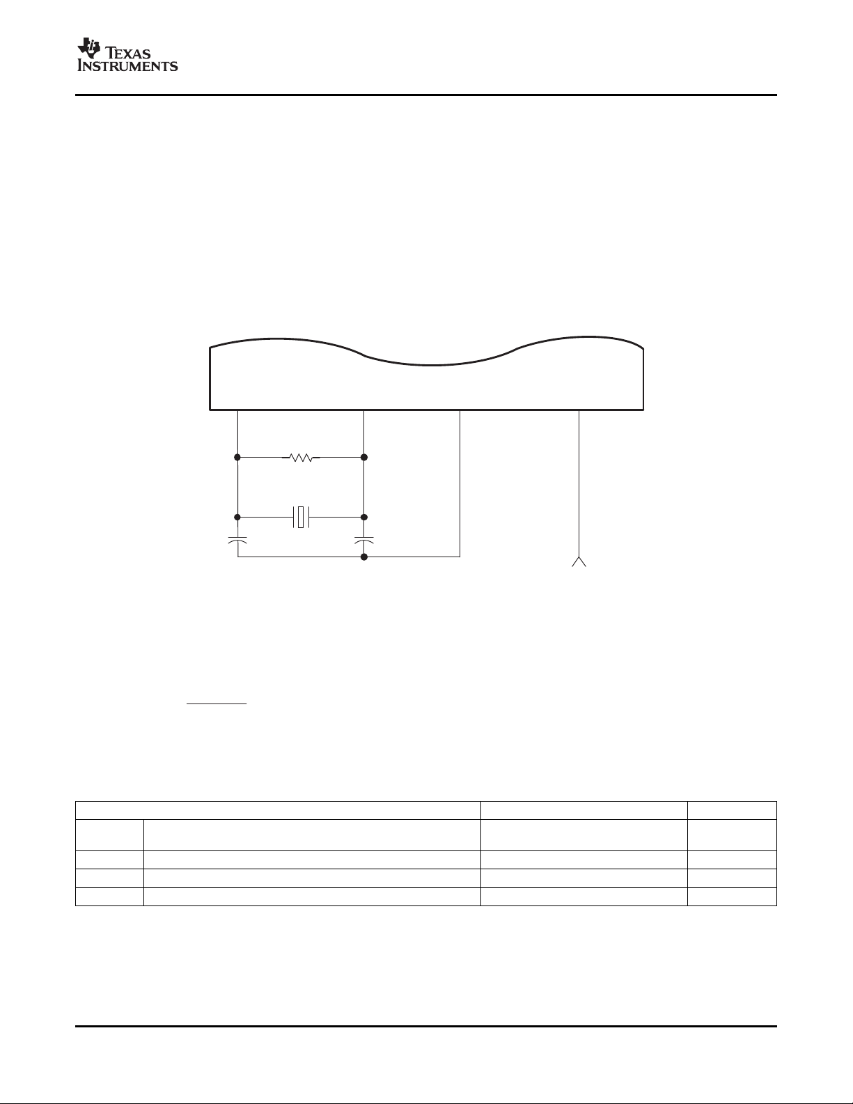
www.ti.com
5.5 Oscillators
MXI/CLKIN MXO
C1 C2
Crystal
MXV
SS
27 MHz
1.8 V
MXV
DD
RBIAS
(optional)
C
L
+
C
1C2
(C1) C2)
DM6441 has two oscillator input/output pairs (MXI/MXO and M24XI/M24XO) usable with external crystals
or ceramic resonators to provide clock inputs. The optimal frequencies for the crystals are 27 MHz
(MXI/MXO) and 24 MHz (M24XI/M24XO). Optionally, the oscillator inputs are configurable for use with
external oscillators.
5.5.1 27-MHz System Oscillator
The 27-MHz oscillator provides the reference clock for all DM6441 subsystems and peripherals, with the
exception of USB. The on-chip oscillator requires an external 27-MHz crystal connected across the MXI
and MXO pins, along with two load capacitors, as shown in Figure 5-10 . The external crystal load
capacitors must be connected only to the 27-MHz oscillator ground pin (MXV
ground (V
TMS320DM6441
Digital Media System-on-Chip
SPRS359B – SEPTEMBER 2006 – REVISED JANUARY 2007
). Do not connect to board
).
SS
SS
The load capacitors, C1 and C2, should be chosen such that the equation is satisfied (typical values are
C1 = C2 = 10 pF). CL in the equation is the load specified by the crystal manufacturer. All discrete
components used to implement the oscillator circuit should be placed as close as possible to the
associated oscillator pins (MXI and MXO) and to the MXV
Table 5-11. Switching Characteristics Over Recommended Operating Conditions for 27-MHz System
Start-up time (from power up until oscillating at stable frequency
of 27 MHz)
Oscillation frequency 27 MHz
ESR 60 Ω
Frequency stability ± 50 ppm
Figure 5-10. 27-MHz System Oscillator
pin.
SS
Oscillator
PARAMETER MIN TYP MAX UNIT
4 ms
Submit Documentation Feedback Peripheral and Electrical Specifications 97

www.ti.com
M24XI M24XO M24V
SS
M24V
DD
C1 C2
Crystal
24 MHz
1.8 V
RBIAS
(optional)
C
L
+
C
1C2
(C1) C2)
TMS320DM6441
Digital Media System-on-Chip
SPRS359B – SEPTEMBER 2006 – REVISED JANUARY 2007
5.5.2 24-MHz USB Oscillator
The 24-MHz oscillator provides the reference clock for the DM6441 USB peripheral. The on-chip oscillator
requires an external 24-MHz crystal connected across the M24XI and M24XO pins, along with two load
capacitors, as shown in Figure 5-11 .The external crystal load capacitors must be connected only to the
24-MHz oscillator ground pin (M24V
). Do not connect to board ground (V
SS
).
SS
Figure 5-11. 24-MHz USB Oscillator
The load capacitors, C1 and C2, should be chosen such that the equation is satisfied (typical values are
C1 = C2 = 10 pF). CL in the equation is the load specified by the crystal manufacturer. All discrete
components used to implement the oscillator circuit should be placed as close as possible to the
associated oscillator pins (M24XI and M24XO) and to the M24XV
pin.
SS
Table 5-12. Switching Characteristics Over Recommended Operating Conditions for 24-MHz System
Oscillator
PARAMETER MIN TYP MAX UNIT
Start-up time (from power up until oscillating at stable frequency
of 24 MHz)
Oscillation frequency 27 MHz
ESR 60 Ω
Frequency stability ± 50 ppm
4 ms
Peripheral and Electrical Specifications98 Submit Documentation Feedback

www.ti.com
5.6 Clock PLLs
There are two independently controlled PLLs on DM6441. PLL1 generates the frequencies required for the
DSP, ARM, VICP, DMA, VPFE, and other peripherals. PLL2 generates the frequencies required for the
DDR2 interface and the VPBE in certain modes. The recommended reference clock for both PLLs is the
27-MHz crystal input. The USB2.0 PHY contains a third PLL embedded within it and the 24-MHz oscillator
is its reference clock source. This particular PLL is only usable for USB operation, and is discussed further
in the DMSoC Universal Serial Bus (USB) Controller User's Guide (literature number SPRUE35 ) [see the
link in the DMSoc Peripherals Overview Reference Guide (literature number SPRUE19 ) in Section 2.8.3 ,
Documentation Support, of this document].
A summary of the PLL controller registers is shown in Table 5-13 . For more details, see the DMSoC ARM
Subsystem Reference Guide (literature number SPRUE14 ) [see Section 2.8.3 , Documentation Support].
Table 5-13. PLL and Reset Controller Registers Memory Map
HEX ADDRESS RANGE REGISTER ACRONYM DESCRIPTION
PLL1 Controller Registers
0x01C4 0800 PID Peripheral Identification and Revision Information Register
0x01C4 08E4 RSTYPE Reset Type Register
0x01C4 0900 PLLCTL PLL Controller 1 Operations Control Register
0x01C4 0910 PLLM PLL Controller 1 Multiplier Control Register
0x01C4 0918 PLLDIV1 PLL Controller 1 Control-Divider 1 Register (SYSCLK1)
0x01C4 091C PLLDIV2 PLL Controller 1 Control-Divider 2 Register (SYSCLK2)
0x01C4 0920 PLLDIV3 PLL Controller 1 Control-Divider 3 Register (SYSCLK3)
0x01C4 0928 POSTDIV PLL Controller 1 Post-Divider Control Register
0x01C4 092C BPDIV PLL Controller 1 Bypass Control-Divider Register (SYSCLKBP)
0x01C4 0938 PLLCMD PLL Controller 1 Command Register
0x01C4 093C PLLSTAT PLL Controller 1 Status Register (Shows PLLCTRL Status)
0x01C4 0940 ALNCTL
0x01C4 0944 DCHANGE
0x01C4 0948 CKEN PLL Controller 1 Clock Enable Register
0x01C4 094C CKSTAT PLL Controller 1 Clock Status Register (For All Clocks Except SYSCLKx)
0x01C4 0950 PLL Controller 1 System Clock Status 1 Register (Indicates SYSCLK on/off
0x01C4 0960 PLLDIV4 PLL Controller 1 Control-Divider 4 Register (SYSCLK4)
0x01C4 0964 PLLDIV5 PLL Controller 1 Control-Divider 5 Register (SYSCLK5)
0x01C4 0C00 PID Peripheral Identification and Revision Information Register
0x01C4 0D00 PLLCTL PLL Controller 2 Operations Control Register
0x01C4 0D10 PLLM PLL Controller 2 Multiplier Control Register
0x01C4 0D18 PLLDIV1 PLL Controller 2 Control-Divider 1 Register (SYSCLK1)
0x01C4 0D1C PLLDIV2 PLL Controller 2 Control-Divider 2 Register (SYSCLK2)
0x01C4 0D20 - 0x01C4 0D2B POSTDIV PLL Controller 2 Post-Divider Control Register
0x01C4 0D2C BPDIV PLL Controller 2 Bypass Control-Divider Register (SYSCLKBP)
0x01C4 0D38 PLLCMD PLL Controller 2 Command Register
0x01C4 0D3C PLLSTAT PLL Controller 2 Status Register (Shows PLLCTRL Status)
0x01C4 0D40 ALNCTL
0x01C4 0D44 DCHANGE
0x01C4 0D48 CKEN PLL Controller 2 Clock Enable Register
SYSTAT
PLL Controller 1 Alignment Control Register
(Indicates Which SYSCLKs Need to be Aligned for Proper Device Operation)
PLL Controller 1 Divider Change Register
(Indicates if SYSCLK Divide Ratio has Been Modified)
Status)
PLL Controller 2 Alignment Control Register
(Indicates Which SYSCLKs Need to be Aligned for Proper Device Operation)
PLL Controller 2 Divider Change Register
(Indicates if SYSCLK Divide Ratio has Been Modified)
TMS320DM6441
Digital Media System-on-Chip
SPRS359B – SEPTEMBER 2006 – REVISED JANUARY 2007
Submit Documentation Feedback Peripheral and Electrical Specifications 99
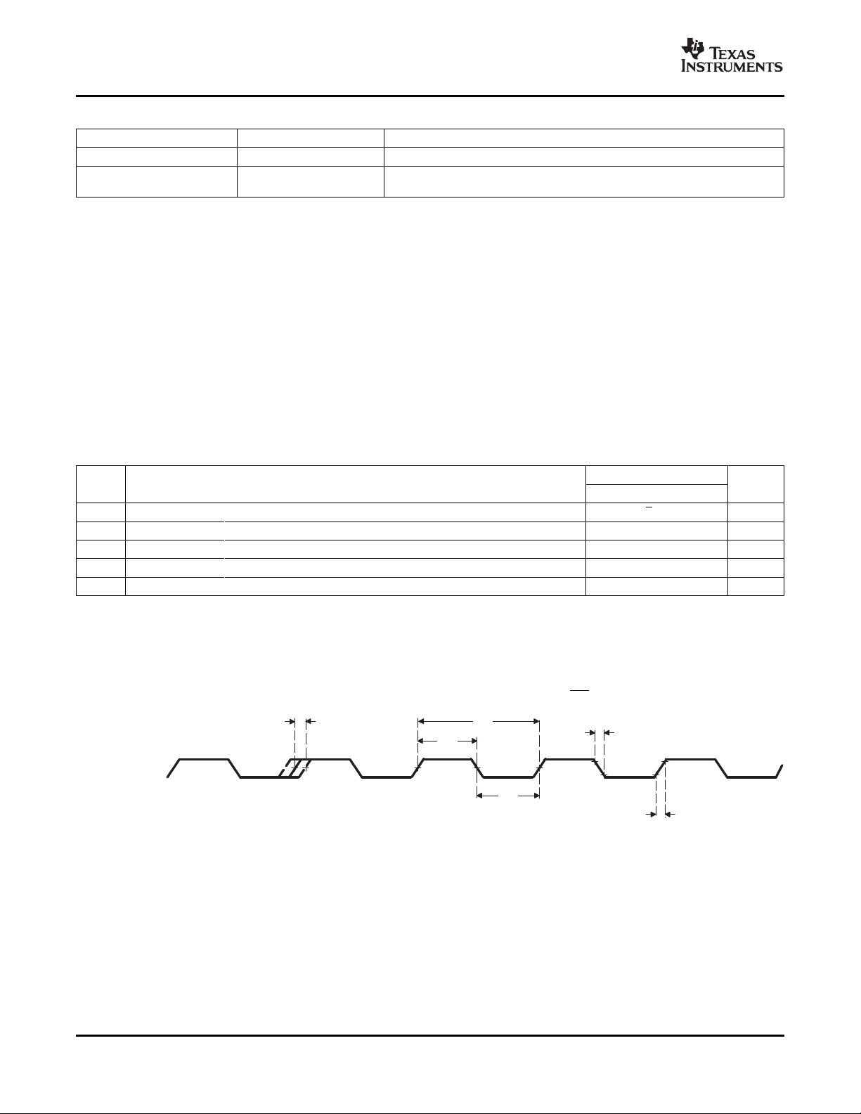
www.ti.com
MXI/CLKIN
2
3
4
4
5
1
TMS320DM6441
Digital Media System-on-Chip
SPRS359B – SEPTEMBER 2006 – REVISED JANUARY 2007
Table 5-13. PLL and Reset Controller Registers Memory Map (continued)
HEX ADDRESS RANGE REGISTER ACRONYM DESCRIPTION
0x01C4 0D4C CKSTAT PLL Controller 2 Clock Status Register (For All Clocks Except SYSCLKx)
0x01C4 0D50 SYSTAT PLL Controller 2 System Clock Status 1 Register (Indicates SYSCLK on/off
5.6.1 Clock PLL Considerations with External Clock Sources
If the internal oscillator is bypassed, to minimize the clock jitter a single clean power supply should power
both the DM6441 device and the external clock oscillator circuit. The minimum CLKIN rise and fall times
should also be observed. For the input clock timing requirements, see Section 5.6.2 , Clock PLL Electrical
Data/Timing (Input and Output Clocks).
Rise/fall times, duty cycles (high/low pulse durations), and the load capacitance of the external clock
source must meet the device requirements in this data manual (see Section 4.3 , Electrical Characteristics
Over Recommended Ranges of Supply Voltage and Operating Case Temperature and Section 5.6.2 ,
Clock PLL Electrical Data/Timing (Input and Output Clocks).
5.6.2 Clock PLL Electrical Data/Timing (Input and Output Clocks)
Status)
Table 5-14. Timing Requirements for MXI/CLKIN Devices
NO. UNIT
1 t
c(MXI)
2 t
w(MXIH)
3 t
w(MXIL)
4 t
t(MXI)
5 t
J(MXI)
(1) Setup before end of STROBE phase (if no extended wait states are inserted) by which EM_WAIT must be asserted to add extended
wait states. Figure 5-21 and Figure 5-22 describe EMIF transactions that include extended wait states inserted during the STROBE
phase. However, cycles inserted as part of this extended wait period should not be counted; the 4E requirement is to the start of where
the HOLD phase would begin if there were no extended wait cycles.
(2) The reference points for the rise and fall transitions are measured at VILMAX and VIHMIN.
(3) For more details on the PLL multiplier factors, see Section 2.8.3 , Documentation Support, for TMS320DM644x ARM Subsystem
Reference Guide.
(4) C = CLKIN cycle time in ns. For example, when MXI/CLKIN frequency is 27 MHz, use C = 37. 037 ns.
Cycle time, MXI/CLKIN 33. 3 50 ns
Pulse duration, MXI/CLKIN high 0.45C 0.55C ns
Pulse duration, MXI/CLKIN low 0.45C 0.55C ns
Transition time, MXI/CLKIN 0.05C ns
Period jitter, MXI/CLKIN 0.02C ns
(1) (2) (3) (4)
(see Figure 5-12 )
1.05 V and 1.2 V
MIN MAX
Figure 5-12. MXI/CLKIN Timing
100 Peripheral and Electrical Specifications Submit Documentation Feedback
 Loading...