


www.ti.com
1 TMS320DM6431 Digital Media Processor
1.1 Features
TMS320DM6431
Digital Media Processor
SPRS342A – NOVEMBER 2006 – REVISED MARCH 2007
• High-Performance Digital Media Processor • C64x+ L1/L2 Memory Architecture
(DM6431)
– 256K-Bit (32K-Byte) L1P Program
– 3.33-ns Instruction Cycle Time RAM/Cache [Flexible Allocation]
– 300-MHz C64x+™ Clock Rate – 256K-Bit (32K-Byte) L1D Data RAM/Cache
[Flexible Allocation]
– Eight 32-Bit C64x+ Instructions/Cycle
– 512K-Bit (64K-Byte) L2 Unified Mapped
– 2400 MIPS
RAM/Cache [Flexible Allocation]
– Fully Software-Compatible With C64x
• Supports Little Endian Mode Only
– Commercial and Extended Temperature
Ranges
• Video Processing Subsystem (VPSS), VPFE
Only
• VelociTI.2™ Extensions to VelociTI™
– Front End Provides:
Advanced Very-Long-Instruction-Word (VLIW)
TMS320C64x+™ DSP Core
• CCD and CMOS Imager Interface
– Eight Highly Independent Functional Units
• BT.601/BT.656 Digital YCbCr 4:2:2
With VelociTI.2 Extensions:
(10-Bit) Interface
• Six ALUs (32-/40-Bit), Each Supports
• Glueless Interface to Common Video
Single 32-Bit, Dual 16-Bit, or Quad 8-Bit
Decoders
Arithmetic per Clock Cycle
• External Memory Interfaces (EMIFs)
• Two Multipliers Support Four 16 x 16-Bit
– 16-Bit DDR2 SDRAM Memory Controller
Multiplies (32-Bit Results) per Clock
With 128M-Byte Address Space (1.8-V I/O)
Cycle or Eight 8 x 8-Bit Multiplies (16-Bit
– Asynchronous 8-Bit Wide EMIF (EMIFA)
Results) per Clock Cycle
With up to 64M-Byte Address Reach
– Load-Store Architecture With Non-Aligned
• Flash Memory Interfaces
Support
• NOR (8-Bit-Wide Data)
– 64 32-Bit General-Purpose Registers
• NAND (8-Bit-Wide Data)
– Instruction Packing Reduces Code Size
• Enhanced Direct-Memory-Access (EDMA)
– All Instructions Conditional
Controller (64 Independent Channels)
– Additional C64x+™ Enhancements
• Two 64-Bit General-Purpose Timers (Each
• Protected Mode Operation
Configurable as Two 32-Bit Timers)
• Exceptions Support for Error Detection
• One 64-Bit Watch Dog Timer
and Program Redirection
• Hardware Support for Modulo Loop
• One UART With RTS and CTS Flow Control
Auto-Focus Module Operation
• Master/Slave Inter-Integrated Circuit (I2C
• C64x+ Instruction Set Features
Bus™)
– Byte-Addressable (8-/16-/32-/64-Bit Data)
• One Multichannel Buffered Serial Port
– 8-Bit Overflow Protection
(McBSP0)
– Bit-Field Extract, Set, Clear
– I2S and TDM
– Normalization, Saturation, Bit-Counting
– AC97 Audio Codec Interface
– VelociTI.2 Increased Orthogonality
– SPI
– C64x+ Extensions
– Standard Voice Codec Interface (AIC12)
• Compact 16-bit Instructions
– Telecom Interfaces – ST-Bus, H-100
• Additional Instructions to Support
– 128 Channel Mode
Complex Multiplies
• Multichannel Audio Serial Port (McASP0)
– Four Serializers and SPDIF (DIT) Mode
• High-End CAN Controller (HECC)
• 10/100 Mb/s Ethernet MAC (EMAC)
Please be aware that an important notice concerning availability, standard warranty, and use in critical applications of Texas
Instruments semiconductor products and disclaimers thereto appears at the end of this document.
All trademarks are the property of their respective owners.
PRODUCT PREVIEW information concerns products in the
Copyright © 2006–2007, Texas Instruments Incorporated
formative or design phase of development. Characteristic data and
other specifications are design goals. Texas Instruments reserves
the right to change or discontinue these products without notice.

www.ti.com
PRODUCT PREVIEW
1.2 Description
TMS320DM6431
Digital Media Processor
SPRS342A – NOVEMBER 2006 – REVISED MARCH 2007
– IEEE 802.3 Compliant
• Packages:
– Supports Media Independent Interface (MII)
– 361-Pin Pb-Free PBGA Package
(ZWT Suffix), 0.8-mm Ball Pitch
– Management Data I/O (MDIO) Module
– 376-Pin Plastic BGA Package
• Three Pulse Width Modulator (PWM) Outputs
(ZDU Suffix), 1.0-mm Ball Pitch
• On-Chip ROM Bootloader
• 0.09- µ m/6-Level Cu Metal Process (CMOS)
• Individual Power-Savings Modes
• 3.3-V and 1.8-V I/O, 1.2-V Internal (-300)
• Flexible PLL Clock Generators
• Applications:
• IEEE-1149.1 (JTAG™)
– Digital Media
Boundary-Scan-Compatible
– Networked Media Encode
• Up to 111 General-Purpose I/O (GPIO) Pins
– Video Imaging
(Multiplexed With Other Device Functions)
The TMS320C64x+™ DSPs (including the TMS320DM6431 device) are the highest-performance
fixed-point DSP generation in the TMS320C6000™ DSP platform. The DM6431 device is based on the
third-generation high-performance, advanced VelociTI™ very-long-instruction-word (VLIW) architecture
developed by Texas Instruments (TI), making these DSPs an excellent choice for digital media
applications. The C64x+™ devices are upward code-compatible from previous devices that are part of the
C6000™ DSP platform. The C64x™ DSPs support added functionality and have an expanded instruction
set from previous devices.
Any reference to the C64x DSP or C64x CPU also applies, unless otherwise noted, to the C64x+ DSP and
C64x+ CPU, respectively.
With performance of up to 2400 million instructions per second (MIPS) at a clock rate of 300 MHz, the
C64x+ core offers solutions to high-performance DSP programming challenges. The DSP core possesses
the operational flexibility of high-speed controllers and the numerical capability of array processors. The
C64x+ DSP core processor has 64 general-purpose registers of 32-bit word length and eight highly
independent functional units—two multipliers for a 32-bit result and six arithmetic logic units (ALUs). The
eight functional units include instructions to accelerate the performance in video and imaging applications.
The DSP core can produce four 16-bit multiply-accumulates (MACs) per cycle for a total of 1200 million
MACs per second (MMACS), or eight 8-bit MACs per cycle for a total of 2400 MMACS. For more details
on the C64x+ DSP, see the TMS320C64x/C64x+ DSP CPU and Instruction Set Reference Guide
(literature number SPRU732 ).
The DM6431 also has application-specific hardware logic, on-chip memory, and additional on-chip
peripherals similar to the other C6000 DSP platform devices. The DM6431 core uses a two-level
cache-based architecture. The Level 1 program memory/cache (L1P) consists of 32K-byte (KB) memory
space that can be configured as mapped memory or direct mapped cache. The Level 1 data/memory
memory/cache (L1D) of 32KB memory space that can be configured as mapped memory or 2-way
set-associative cache. The Level 2 memory/cache (L2) consists of a 64KB memory space that is shared
between program and data space. L2 memory can be configured as mapped memory, cache, or a
combination of both.
The peripheral set includes: 1 configurable video port; a 10/100 Mb/s Ethernet MAC (EMAC) with a
management data input/output (MDIO) module; an inter-integrated circuit (I2C) Bus interface; a
multichannel buffered serial port (McBSP0); a multichannel audio serial port (McASP0) with 4 serializers; 2
64-bit general-purpose timers each configurable as 2 independent 32-bit timers; 1 64-bit watchdog timer;
up to 111-pins of general-purpose input/output (GPIO) with programmable interrupt/event generation
modes, multiplexed with other peripherals; 1 UART with hardware handshaking support; 3 pulse width
modulator (PWM) peripherals; 1 high-end controller area network (CAN) controller [HECC]; and 2 glueless
external memory interfaces: an asynchronous external memory interface (EMIFA) for slower
memories/peripherals, and a higher speed synchronous memory interface for DDR2.
TMS320DM6431 Digital Media Processor2 Submit Documentation Feedback

www.ti.com
TMS320DM6431
Digital Media Processor
SPRS342A – NOVEMBER 2006 – REVISED MARCH 2007
The DM6431 device includes a Video Processing Subsystem (VPSS) with a Video Processing Front-End
(VPFE) input used for video capture.
The Video Processing Front-End (VPFE) is comprised of a CCD Controller (CCDC). The CCDC is capable
of interfacing to common video decoders, CMOS sensors, and Charge Coupled Devices (CCDs).
The Ethernet Media Access Controller (EMAC) provides an efficient interface between the DM6431 and
the network. The DM6431 EMAC support both 10Base-T and 100Base-TX, or 10 Mbits/second (Mbps)
and 100 Mbps in either half- or full-duplex mode, with hardware flow control and quality of service (QOS)
support.
The Management Data Input/Output (MDIO) module continuously polls all 32 MDIO addresses in order to
enumerate all PHY devices in the system.
The I2C port allows DM6431 to easily control peripheral devices and/or communicate with host
processors.
The high-end controller area network (CAN) controller [HECC] module provides a network protocol in a
harsh environment to communicate serially with other controllers, typically in automotive applications.
The rich peripheral set provides the ability to control external peripheral devices and communicate with
external processors. For details on each of the peripherals, see the related sections later in this document
and the associated peripheral reference guides.
The DM6431 has a complete set of development tools. These include C compilers, a DSP assembly
optimizer to simplify programming and scheduling, and a Windows™ debugger interface for visibility into
source code execution.
Submit Documentation Feedback TMS320DM6431 Digital Media Processor 3

www.ti.com
PRODUCT PREVIEW
1.3 Functional Block Diagram
JTAG Interface
System Control
PLLs/Clock Generator
Input
Clock(s)
Power/Sleep Controller
Pin Multiplexing
DSP Subsystem
C64x+t DSP CPU
32 KB
L1 Pgm
64 KB L2 RAM
32 KB
L1 Data
BT.656,
Y/C,
Raw (Bayer)
Video Processing Subsystem (VPSS)
CCD
Controller
Video
Interface
Front End
Switched Central Resource (SCR)
Peripherals
EDMA
I2C HECC UART
Serial Interfaces
DDR2
Mem Ctlr
(16b)
Async EMIF/
NAND/
(8b)
Program/Data Storage
Watchdog
Timer
PWM
System
GeneralPurpose
Timer
EMAC
With
MDIO
Connectivity
McASP
McBSP
OSC
Boot ROM
10b
GPIO
TMS320DM6431
Digital Media Processor
SPRS342A – NOVEMBER 2006 – REVISED MARCH 2007
Figure 1-1 shows the functional block diagram of the DM6431 device.
Figure 1-1. TMS320DM6431 Functional Block Diagram
TMS320DM6431 Digital Media Processor4 Submit Documentation Feedback

www.ti.com
Contents
TMS320DM6431
Digital Media Processor
SPRS342A – NOVEMBER 2006 – REVISED MARCH 2007
5.3 Electrical Characteristics Over Recommended
1 TMS320DM6431 Digital Media Processor ........... 1
Ranges of Supply Voltage and Operating
1.1 Features .............................................. 1
Temperature (Unless Otherwise Noted) ........... 119
1.2 Description ............................................ 2
6 Peripheral Information and Electrical
1.3 Functional Block Diagram ............................ 4
Specifications ......................................... 120
Revision History ............................................... 6
6.1 Parameter Information ............................. 120
2 Device Overview ......................................... 7
6.2 Recommended Clock and Control Signal Transition
Behavior ............................................ 121
2.1 Device Characteristics ................................ 7
6.3 Power Supplies .................................... 122
2.2 CPU (DSP Core) Description ......................... 8
6.4 Enhanced Direct Memory Access (EDMA3)
2.3 C64x+ CPU .......................................... 11
Controller ........................................... 129
2.4 Memory Map Summary ............................. 12
6.5 Reset ............................................... 141
2.5 Pin Assignments .................................... 16
6.6 External Clock Input From MXI/CLKIN Pin ........ 150
2.6 Terminal Functions .................................. 24
6.7 Clock PLLs ......................................... 152
2.7 Device Support ...................................... 56
6.8 Interrupts ........................................... 157
2.8 Device and Development-Support Tool
6.9 External Memory Interface (EMIF) ................. 160
Nomenclature ....................................... 56
6.10 Video Processing Sub-System (VPSS) Overview . 169
2.9 Documentation Support ............................. 58
6.11 Universal Asynchronous Receiver/Transmitter
3 Device Configurations ................................. 59
(UART) ............................................. 174
3.1 System Module Registers ........................... 59
6.12 Inter-Integrated Circuit (I2C) ....................... 176
3.2 Power Considerations ............................... 60
6.13 Multichannel Buffered Serial Port (McBSP) ........ 180
3.3 Clock Considerations ................................ 62
6.14 Multichannel Audio Serial Port (McASP0)
3.4 Boot Sequence ...................................... 64
Peripheral .......................................... 188
3.5 Configurations At Reset ............................. 74
6.15 High-End Controller Area Network Controller
3.6 Configurations After Reset .......................... 75
(HECC) ............................................. 196
3.7 Multiplexed Pin Configurations ...................... 79
6.16 Ethernet Media Access Controller (EMAC) ........ 202
3.8 Device Initialization Sequence After Reset ........ 112
6.17 Management Data Input/Output (MDIO) .......... 209
3.9 Debugging Considerations ......................... 114
6.18 Timers .............................................. 211
4 System Interconnect ................................. 115
6.19 Pulse Width Modulator (PWM) ..................... 213
4.1 System Interconnect Block Diagram ............... 115
6.20 General-Purpose Input/Output (GPIO) ............. 215
5 Device Operating Conditions ....................... 117
6.21 IEEE 1149.1 JTAG ................................. 219
5.1 Absolute Maximum Ratings Over Operating
7 Mechanical Data ....................................... 221
Temperature Range (Unless Otherwise Noted) ... 117
7.1 Thermal Data for ZWT ............................. 221
5.2 Recommended Operating Conditions ............. 118
7.1.1 Thermal Data for ZDU ............................. 222
7.1.2 Packaging Information ............................. 222
Submit Documentation Feedback Contents 5

www.ti.com
PRODUCT PREVIEW
Revision History
TMS320DM6431
Digital Media Processor
SPRS342A – NOVEMBER 2006 – REVISED MARCH 2007
This data manual revision history highlights the technical changes made to the SPRS342 device-specific
data manual to make it an SPRS342A revision.
Scope: Applicable updates to the device family, specifically relating to the device, have been
incorporated.
• The RSV1 pin (E5, D4) must be left unconnected. Do not connect to power or ground.
• Upon exit from the bootloader code, all C64x+ memories are configured as all RAM, Cache is disabled.
• This is now a complete document. New sections and subsections have been added.
SEE ADDITIONS/MODIFICATIONS/DELETIONS
Global Added section cross-references throughout the entire document
Section 1.1 Section 1.1 , Features:
Deleted "/Debug" from the "Fully Software-Compatible With C64x" feature
Section 2.1 Section 2.1 , Device Characteristics:
Table 2-1 , Characteristics of the DM6431 Processor:
Added "MegaMdodule Rev ID"
Updated/Changed the "CPU ID + CPU Rev ID" row to reference the " TMS320DM6437/35/33/31 Digital
Media Processor (DMP) [Silicon Revisions 1.1 and 1.0] Silicon Errata (literature number SPRZ250 )."
Updated/Changed PLL Options " CLKIN1 frequency multiplier (27 MHz reference)" to " MXI/CLKIN
frequency multiplier (27 MHz reference)"
Section 2.4 Section 2.4 , Memory Map Summary:
Section 2.4 , Memory Map Summary:
Added "For all boot modes that default to ..." footnote
Table 2-4 , Configuration Memory Map Summary:
Deleted 0x01BC 0000 — 0x01BC 00FF AET Registers; now "Reserved"
Section 2.6 Section 2.6 , Terminal Functions:
Table 2-5 , Boot Terminal Functions:
Updated/Changed Bootmode[3:0] Descriptions to reference Section 3.4.1 , Boot Modes
Updated/Changed EM_BA[1:0]/(AEM0:1) DSECRIPTION from "...pinout type" to ..."pinout mode"
Table 2-10 , EMIFA Terminal Functions (EMIFA Pinout Mode 1, AEM[2:0] = 001):
Updated/Changed the DESCRIPTION for EM_A[12:0]
Table 2-11 , EMIFA Terminal Functions (EMIFA Pinout Mode 5, AEM[2:0] = 101):
Updated/Changed DESPCRIPTION for EM_CS2/GP[12]
Table 2-12 , DDR2 Memory Controller Terminal Functions:
Added "Output" pin direction to the DESCRIPTION for all address bus and control signals
Added "bi-directional" to the DESCRIPTION for the DDR2 data bus
Table 2-13 , EMAC and MDIO Terminal Functions:
Updated/Changed the "MTXCLK/GP[73]" DESCRIPTION from "output" to "input"
Updated/Changed the "MTXD0/GP[72]" DESCRIPTION from "TXD0" to " MTXD0"
Updated/Changed the "MRXD3/GP[82]" DESCRIPTION from "RXD3" to " MRXD3"
Added " (I/O/Z)" to the MDIO/GP[83] DESCRIPTION
Table 2-14 , VPFE Terminal Functions:
Updated/Changed the DESCRIPTION for the following signals: CCDC9 through CCDC0 from "CCD AFE
mode" to "CCD Raw mode"
Added "In 8-bit YCbCr mode, this pin should not be used." to the DESCRIPTION for CCD8 and CCD9
Table 2-23 , Standalone GPIO 3.3 V Terminal Functions:
Updated/Changed the DESCRIPTION for GP[28] to "... pulled down via an external resistor"
Table 2-24 , Reserved Terminal Functions:
Deleted TYPE for the following signals: RSV4 through RSV15
Section 2.8 Section 2.8 , Device and Development-Support Tool Nomenclature:
Updated/Changed Figure 2-10 , Device Nomenclature
Section 5.3 Section 5.3 , Electrical Characteristics Over Recommended Ranges of Supply Voltage and Operating
Temperature (Unless Otherwise Noted):
Updated/Changed CIand COMAX values from "10 pF" to "5 pF"
Updated/Changed the "Measured under the following conditions: ..." footnote
6 Revision History Submit Documentation Feedback
www.ti.com
2 Device Overview
2.1 Device Characteristics
TMS320DM6431
Digital Media Processor
SPRS342A – NOVEMBER 2006 – REVISED MARCH 2007
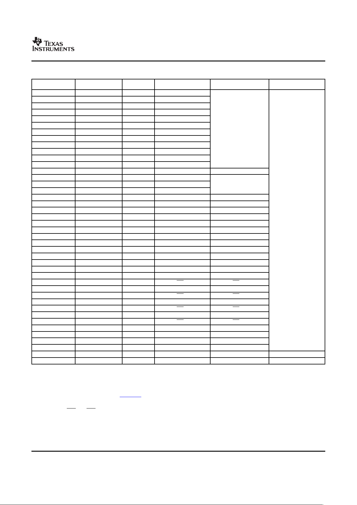
Table 2-1 , provides an overview of the TMS320DM6431 DSP. The tables show significant features of the
DM6431 device, including the capacity of on-chip RAM, the peripherals, the CPU frequency, and the
package type with pin count.
Table 2-1. Characteristics of the DM6431 Processor
HARDWARE FEATURES DM6431
DDR2 Memory Controller (16-bit bus width) [1.8 V I/O]
Asynchronous (8-bit bus width),
Asynchronous EMIF [EMIFA]
RAM, Flash, (8-bit NOR or 8-bit NAND)
EDMA3 1 (64 independent channels, 8 QDMA channels)
2 64-bit General Purpose
Timers (configurable as 2 64-bit or 4 32-bit)
1 64-bit Watch Dog
Peripherals
UART 1 (with RTS and CTS flow control)
Not all peripherals pins
I2C 1 (Master/Slave)
are available at the same
time (For more detail, see
McBSP 1
the Device Configuration
McASP 1 (4 serailizers)
section).
10/100 Ethernet MAC (EMAC) with
1
Management Data Input/Output (MDIO)
General-Purpose Input/Output Port (GPIO) Up to 111 pins
PWM 3 outputs
Configurable Video Port 1 Input (VPFE)
HECC 1
Size (Bytes) 128KB RAM, 64KB ROM
32K-Byte (32KB) L1 Program (L1P) RAM/Cache
(Cache up to 32KB)
On-Chip Memory
Organization 32KB L1 Data (L1D) RAM/Cache (Cache up to 32KB)
64KB Unified Mapped RAM/Cache (L2)
64KB Boot ROM
Revision ID Register (MM_REVID.[15:0])
See the TMS320DM6437/35/33/31 Digital Media
MegaModule Rev ID
(address location: 0x0181 2000)
Processor (DMP) [Silicon Revisions 1.1 and 1.0]
Silicon Errata (literature number SPRZ250 ).
CPU ID + CPU Rev ID Control Status Register (CSR.[31:16])
JTAGID register See Section 6.21.1 , JTAG ID (JTAGID) Register
JTAG BSDL_ID
(address location: 0x01C4 0028) Description(s)
CPU Frequency MHz 300
Cycle Time ns 3.33 ns (-300)
Core (V) 1.2 V (-300)
Voltage
I/O (V) 1.8 V, 3.3 V
MXI/CLKIN frequency multiplier
PLL Options x1 (Bypass), x14 to x30
(27 MHz reference)
16 x 16 mm, 0.8 mm pitch 361-Pin BGA (ZWT)
BGA Package(s)
23 x 23 mm, 1.0 mm pitch 376-Pin BGA (ZDU)
Process Technology µm 0.09 µm
Product Preview (PP), Advance Information (AI),
Product Status
(1)
PP
or Production Data (PD)
(1) PRODUCT PREVIEW information concerns experimental products (designated as TMX) that are in the formative or design phase of
development. Characteristic data and other specifications are design goals. Texas Instruments reserves the right to change or
discontinue these products without notice.
Submit Documentation Feedback Device Overview 7

www.ti.com
PRODUCT PREVIEW
2.2 CPU (DSP Core) Description
TMS320DM6431
Digital Media Processor
SPRS342A – NOVEMBER 2006 – REVISED MARCH 2007
The C64x+ Central Processing Unit (CPU) consists of eight functional units, two register files, and two
data paths as shown in Figure 2-1 . The two general-purpose register files (A and B) each contain
32 32-bit registers for a total of 64 registers. The general-purpose registers can be used for data or can be
data address pointers. The data types supported include packed 8-bit data, packed 16-bit data, 32-bit
data, 40-bit data, and 64-bit data. Values larger than 32 bits, such as 40-bit-long or 64-bit-long values are
stored in register pairs, with the 32 LSBs of data placed in an even register and the remaining 8 or
32 MSBs in the next upper register (which is always an odd-numbered register).
The eight functional units (.M1, .L1, .D1, .S1, .M2, .L2, .D2, and .S2) are each capable of executing one
instruction every clock cycle. The .M functional units perform all multiply operations. The .S and .L units
perform a general set of arithmetic, logical, and branch functions. The .D units primarily load data from
memory to the register file and store results from the register file into memory.
The C64x+ CPU extends the performance of the C64x core through enhancements and new features.
Each C64x+ .M unit can perform one of the following each clock cycle: one 32 x 32 bit multiply, one 16 x
32 bit multiply, two 16 x 16 bit multiplies, two 16 x 32 bit multiplies, two 16 x 16 bit multiplies with
add/subtract capabilities, four 8 x 8 bit multiplies, four 8 x 8 bit multiplies with add operations, and four
16 x 16 multiplies with add/subtract capabilities (including a complex multiply). There is also support for
Galois field multiplication for 8-bit and 32-bit data. Many communications algorithms such as FFTs and
modems require complex multiplication. The complex multiply (CMPY) instruction takes for 16-bit inputs
and produces a 32-bit real and a 32-bit imaginary output. There are also complex multiplies with rounding
capability that produces one 32-bit packed output that contain 16-bit real and 16-bit imaginary values. The
32 x 32 bit multiply instructions provide the extended precision necessary for audio and other
high-precision algorithms on a variety of signed and unsigned 32-bit data types.
The .L or (Arithmetic Logic Unit) now incorporates the ability to do parallel add/subtract operations on a
pair of common inputs. Versions of this instruction exist to work on 32-bit data or on pairs of 16-bit data
performing dual 16-bit add and subtracts in parallel. There are also saturated forms of these instructions.
The C64x+ core enhances the .S unit in several ways. In the C64x core, dual 16-bit MIN2 and MAX2
comparisons were only available on the .L units. On the C64x+ core they are also available on the .S unit
which increases the performance of algorithms that do searching and sorting. Finally, to increase data
packing and unpacking throughput, the .S unit allows sustained high performance for the quad 8-bit/16-bit
and dual 16-bit instructions. Unpack instructions prepare 8-bit data for parallel 16-bit operations. Pack
instructions return parallel results to output precision including saturation support.
Other new features include:
• SPLOOP - A small instruction buffer in the CPU that aids in creation of software pipelining loops where
multiple iterations of a loop are executed in parallel. The SPLOOP buffer reduces the code size
associated with software pipelining. Furthermore, loops in the SPLOOP buffer are fully interruptible.
• Compact Instructions - The native instruction size for the C6000 devices is 32 bits. Many common
instructions such as MPY, AND, OR, ADD, and SUB can be expressed as 16 bits if the C64x+
compiler can restrict the code to use certain registers in the register file. This compression is
performed by the code generation tools.
Device Overview8 Submit Documentation Feedback

www.ti.com
TMS320DM6431
Digital Media Processor
SPRS342A – NOVEMBER 2006 – REVISED MARCH 2007
• Instruction Set Enhancement - As noted above, there are new instructions such as 32-bit
multiplications, complex multiplications, packing, sorting, bit manipulation, and 32-bit Galois field
multiplication.
• Exceptions Handling - Intended to aid the programmer in isolating bugs. The C64x+ CPU is able to
detect and respond to exceptions, both from internally detected sources (such as illegal op-codes) and
from system events (such as a watchdog time expiration).
• Privilege - Defines user and supervisor modes of operation, allowing the operating system to give a
basic level of protection to sensitive resources. Local memory is divided into multiple pages, each with
read, write, and execute permissions.
• Time-Stamp Counter - Primarily targeted for Real-Time Operating System (RTOS) robustness, a
free-running time-stamp counter is implemented in the CPU which is not sensitive to system stalls.
For more details on the C64x+ CPU and its enhancements over the C64x architecture, see the following
documents:
• TMS320C64x/C64x+ DSP CPU and Instruction Set Reference Guide (literature number SPRU732 )
• TMS320C64x+ DSP Megamodule Reference Guide (literature number SPRU871 )
• TMS320C64x to TMS320C64x+ CPU Migration Guide Application Report (literature number SPRAA84 )
• TMS320C64x+ DSP Cache User's Guide (literature number SPRU862 )
Submit Documentation Feedback Device Overview 9
www.ti.com
PRODUCT PREVIEW
src2
src2
.D1
.M1
.S1
.L1
long src
odd dst
src2
src1
src1
src1
src1
even dst
even dst
odd dst
dst1
dst
src2
src2
src2
long src
DA1
ST1b
LD1b
LD1a
ST1a
Data path A
Odd
register
file A
(A1, A3,
A5...A31)
Odd
register
file B
(B1, B3,
B5...B31)
.D2
src1
dst
src2
DA2
LD2a
LD2b
src2
.M2
src1
dst1
.S2
src1
even dst
long src
odd dst
ST2a
ST2b
long src
.L2
even dst
odd dst
src1
Data path B
Control Register
32 MSB
32 LSB
dst2
(A)
32 MSB
32 LSB
2x
1x
32 LSB
32 MSB
32 LSB
32 MSB
dst2
(B)
(B)
(A)
8
8
8
8
32
32
32
32
(C)
(C)
Even
register
file A
(A0, A2,
A4...A30)
Even
register
file B
(B0, B2,
B4...B30)
(D)
(D)
(D)
(D)
A. On .M unit, dst2 is 32 MSB.
B. On .M unit, dst1 is 32 LSB.
C. On C64x CPU .M unit, src2 is 32 bits; on C64x+ CPU .M unit, src2 is 64 bits.
D. On .L and .S units, odd dst connects to odd register files and even dst connects to even register files.
TMS320DM6431
Digital Media Processor
SPRS342A – NOVEMBER 2006 – REVISED MARCH 2007
Figure 2-1. TMS320C64x+™ CPU (DSP Core) Data Paths
10 Device Overview Submit Documentation Feedback
www.ti.com
2.3 C64x+ CPU
TMS320DM6431
Digital Media Processor
SPRS342A – NOVEMBER 2006 – REVISED MARCH 2007
The C64x+ core uses a two-level cache-based architecture. The Level 1 Program memory/cache (L1P)
consists of 32 KB memory space that can be configured as mapped memory or direct mapped cache. The
Level 1 Data memory/cache (L1D) consists of 32 KB memory space that can be configured as mapped
memory or 2-way set associated cache. The Level 2 memory/cache (L2) consists of a 64 KB memory
space that is shared between program and data space. L2 memory can be configured as mapped
memory, cache, or a combination of both.
Table 2-2 shows a memory map of the C64x+ CPU cache registers for the device.
Table 2-2. C64x+ Cache Registers
HEX ADDRESS RANGE REGISTER ACRONYM DESCRIPTION
0x0184 0000 L2CFG L2 Cache configuration register
0x0184 0020 L1PCFG L1P Size Cache configuration register
0x0184 0024 L1PCC L1P Freeze Mode Cache configuration register
0x0184 0040 L1DCFG L1D Size Cache configuration register
0x0184 0044 L1DCC L1D Freeze Mode Cache configuration register
0x0184 0048 - 0x0184 0FFC - Reserved
0x0184 1000 EDMAWEIGHT L2 EDMA access control register
0x0184 1004 - 0x0184 1FFC - Reserved
0x0184 2000 L2ALLOC0 L2 allocation register 0
0x0184 2004 L2ALLOC1 L2 allocation register 1
0x0184 2008 L2ALLOC2 L2 allocation register 2
0x0184 200C L2ALLOC3 L2 allocation register 3
0x0184 2010 - 0x0184 3FFF - Reserved
0x0184 4000 L2WBAR L2 writeback base address register
0x0184 4004 L2WWC L2 writeback word count register
0x0184 4010 L2WIBAR L2 writeback invalidate base address register
0x0184 4014 L2WIWC L2 writeback invalidate word count register
0x0184 4018 L2IBAR L2 invalidate base address register
0x0184 401C L2IWC L2 invalidate word count register
0x0184 4020 L1PIBAR L1P invalidate base address register
0x0184 4024 L1PIWC L1P invalidate word count register
0x0184 4030 L1DWIBAR L1D writeback invalidate base address register
0x0184 4034 L1DWIWC L1D writeback invalidate word count register
0x0184 4038 - Reserved
0x0184 4040 L1DWBAR L1D Block Writeback
0x0184 4044 L1DWWC L1D Block Writeback
0x0184 4048 L1DIBAR L1D invalidate base address register
0x0184 404C L1DIWC L1D invalidate word count register
0x0184 4050 - 0x0184 4FFF - Reserved
0x0184 5000 L2WB L2 writeback all register
0x0184 5004 L2WBINV L2 writeback invalidate all register
0x0184 5008 L2INV L2 Global Invalidate without writeback
0x0184 500C - 0x0184 5027 - Reserved
0x0184 5028 L1PINV L1P Global Invalidate
0x0184 502C - 0x0184 5039 - Reserved
0x0184 5040 L1DWB L1D Global Writeback
0x0184 5044 L1DWBINV L1D Global Writeback with Invalidate
Submit Documentation Feedback Device Overview 11
www.ti.com
PRODUCT PREVIEW
2.4 Memory Map Summary
TMS320DM6431
Digital Media Processor
SPRS342A – NOVEMBER 2006 – REVISED MARCH 2007
Table 2-2. C64x+ Cache Registers (continued)
HEX ADDRESS RANGE REGISTER ACRONYM DESCRIPTION
0x0184 5048 L1DINV L1D Global Invalidate without writeback
0x0184 8000 - 0x0184 80BC MAR0 - MAR47 Reserved (corresponds to byte address 0x0000 0000 - 0x2FFF FFFF)
0x0184 80C0 - 0x0184 80FC MAR48 - MAR63 Reserved (corresponds to byte address 0x3000 0000 - 0x3FFF FFFF)
0x0184 8100 - 0x0184 8104 MAR64 - MAR65 Reserved (corresponds to byte address 0x4000 0000 - 0x41FF FFFF)
Memory Attribute Registers for EMIFA
0x0184 8108 - 0x0184 8124 MAR66 - MAR73
(corresponds to byte address 0x4200 0000 - 0x49FF FFFF)
0x0184 8128 - 0x0184 812C MAR74 - MAR75 Reserved (corresponds to byte address 0x4A00 0000 - 0x4BFF FFFF)
0x0184 8130 - 0x0184 813C MAR76 - MAR79 Reserved (corresponds to byte address 0x4C00 0000 - 0x4FFF FFFF)
0x0184 8140- 0x0184 81FC MAR80 - MAR127 Reserved (corresponds to byte address 0x5000 0000 - 0x7FFF FFFF)
Memory Attribute Registers for DDR2
0x0184 8200 - 0x0184 823C MAR128 - MAR143
(corresponds to byte address 0x8000 0000 - 0x8FFF FFFF)
0x0184 8240 - 0x0184 83FC MAR144 - MAR255 Reserved (corresponds to byte address 0x9000 0000 - 0xFFFF FFFF)
Table 2-3 shows the memory map address ranges of the device. Table 2-4 depicts the expanded map of
the Configuration Space (0x0180 0000 through 0x0FFF FFFF). The device has multiple on-chip memories
associated with its two processors and various subsystems. To help simplify software development a
unified memory map is used where possible to maintain a consistent view of device resources across all
bus masters.
Device Overview12 Submit Documentation Feedback
www.ti.com
TMS320DM6431
Digital Media Processor
SPRS342A – NOVEMBER 2006 – REVISED MARCH 2007
Table 2-3. Memory Map Summary
START END SIZE C64x+ EDMA PERIPHERAL VPSS
ADDRESS ADDRESS (Bytes) MEMORY MAP MEMORY MAP MEMORY MAP
0x0000 0000 0x000F FFFF 1M Reserved
0x0010 0000 0x0010 FFFF 64K Boot ROM
0x0011 0000 0x007F FFFF 7M-64K Reserved
0x0080 0000 0x0080 FFFF 64K Reserved
0x0081 0000 0x0081 FFFF 64K L2 RAM/Cache
(1)
0x0082 0000 0x00E0 7FFF 6048K Reserved
Reserved
0x00E0 8000 0x00E0 FFFF 32K L1P RAM/Cache
(1)
0x00E1 0000 0x00F0 3FFF 976K Reserved
0x00F0 4000 0x00F0 FFFF 48K Reserved
0x00F1 0000 0x00F1 7FFF 32K L1D RAM/Cache
(1)
0x00F1 8000 0x017F FFFF 9120K Reserved
0x0180 0000 0x01BF FFFF 4M CFG Space
0x01C0 0000 0x01FF FFFF 4M CFG Bus Peripherals CFG Bus Peripherals
0x0200 0000 0x100F FFFF 225M Reserved
0x1010 0000 0x1010 FFFF 64K Boot ROM Reserved
0x1011 0000 0x107F FFFF 7M-48K Reserved
0x1080 0000 0x1080 FFFF 64K Reserved Reserved
0x1081 0000 0x1081 FFFF 64K L2 RAM/Cache
(1)
L2 RAM/Cache
(1)
0x1082 0000 0x10E0 7FFF 6048K Reserved Reserved
0x10E0 8000 0x10E0 FFFF 32K L1P RAM/Cache
(1)
L1P RAM/Cache
(1)
Reserved
0x10E1 0000 0x10F0 3FFF 976K Reserved Reserved
0x10F0 4000 0x10F0 FFFF 48K Reserved Reserved
0x10F1 0000 0x10F1 7FFF 32K L1D RAM/Cache
(1)
L1D RAM/Cache
(1)
0x10F1 8000 0x10FF FFFF 1M-96K Reserved Reserved
0x1100 0000 0x1FFF FFFF 240M Reserved Reserved
0x2000 0000 0x2000 7FFF 32K DDR2 Control Regs DDR2 Control Regs
0x2000 8000 0x2FFF FFFF 256M-32K Reserved Reserved
0x3000 0000 0x3FFF FFFF 256M Reserved Reserved
0x4000 0000 0x41FF FFFF 32M Reserved Reserved
0x4200 0000 0x42FF FFFF 16M EMIFA Data ( CS2)
(2)
EMIFA Data ( CS2)
(2)
0x4300 0000 0x43FF FFFF 16M Reserved Reserved
0x4400 0000 0x44FF FFFF 16M EMIFA Data ( CS3)
(2)
EMIFA Data ( CS3)
(2)
0x4500 0000 0x45FF FFFF 16M Reserved Reserved
0x4600 0000 0x46FF FFFF 16M EMIFA Data ( CS4)
(2)
EMIFA Data ( CS4)
(2)
0x4700 0000 0x47FF FFFF 16M Reserved Reserved
0x4800 0000 0x48FF FFFF 16M EMIFA Data ( CS5)
(2)
EMIFA Data ( CS5)
(2)
0x4900 0000 0x49FF FFFF 16M Reserved Reserved
0x4A00 0000 0x4BFF FFFF 32M Reserved Reserved
0x4C00 0000 0x4FFF FFFF 64M Reserved Reserved
0x5000 0000 0x7FFF FFFF 768M Reserved Reserved
0x8000 0000 0x8FFF FFFF 256M DDR2 Memory Controller DDR2 Memory Controller DDR2 Memory Controller
0x9000 0000 0xFFFF FFFF 1792M Reserved Reserved Reserved
(1) For all bootmodes that default to DSPBOOTADDR = 0x0010 0000 (i.e., all boot modes except the EMIFA ROM Direct Boot,
BOOTMODE[3:0] = 0100, FASTBOOT = 0), the bootloader code disables all C64x+ cache (L2, L1P, and L1D) so that upon exit from the
bootloader code, all C64x+ memories are configured as all RAM (L2CFG.L2MODE = 0h, L1PCFG.L1PMODE = 0h, and
L1DCFG.L1DMODE = 0h). If cache use is required, the application code must explicitly enable the cache. For more information on boot
modes, see Section 3.4.1 , Boot Modes. For more information on the bootloader, see the Using the TMS320DM643x Bootloader
Application Report (literature number SPRAAG0 ). For the EMIFA ROM Direct Boot (BOOTMODE[3:0] = 0100, FASTBOOT = 0), the
bootloader is not executed—that is, L2 RAM/Cache defaults to all RAM (L2CFG.L2MODE = 0h); L1P RAM/Cache defaults to all cache
(L1PCFG.L1PMODE = 7h); and L1D RAM/Cache defaults to all cache (L1DCFG.L1DMODE = 7h).
(2) The EMIFA CS0 and CS1 are not functionally supported on the DM6431 device, and therefore, are not pinned out.
Submit Documentation Feedback Device Overview 13
www.ti.com
PRODUCT PREVIEW
TMS320DM6431
Digital Media Processor
SPRS342A – NOVEMBER 2006 – REVISED MARCH 2007
Table 2-4. Configuration Memory Map Summary
START END SIZE C64x+
ADDRESS ADDRESS (Bytes)
0x0180 0000 0x0180 FFFF 64K C64x+ Interrupt Controller
0x0181 0000 0x0181 0FFF 4K C64x+ Powerdown Controller
0x0181 1000 0x0181 1FFF 4K C64x+ Security ID
0x0181 2000 0x0181 2FFF 4K C64x+ Revision ID
0x0182 0000 0x0182 FFFF 64K C64x+ EMC
0x0183 0000 0x0183 FFFF 64K Reserved
0x0184 0000 0x0184 FFFF 64K C64x+ Memory System
0x0185 0000 0x0187 FFFF 192K Reserved
0x0188 0000 0x01BB FFFF 3328K Reserved
0x01BC 0000 0x01BC 00FF 256 Reserved
0x01BC 0100 0x01BC 01FF 256 Pin Manager and Trace
0x01BC 0400 0x01BF FFFF 255K Reserved
0x01C0 0000 0x01C0 FFFF 64K EDMA CC
0x01C1 0000 0x01C1 03FF 1K EDMA TC0
0x01C1 0400 0x01C1 07FF 1K EDMA TC1
0x01C1 0800 0x01C1 0BFF 1K EDMA TC2
0x01C1 0C00 0x01C1 9FFF 5K Reserved
0x01C1 A000 0x01C1 A7FF 2K Reserved
0x01C1 A800 0x01C1 FFFF 22K Reserved
0x01C2 0000 0x01C2 03FF 1K UART0
0x01C2 0400 0x01C2 07FF 1K Reserved
0x01C2 0800 0x01C2 0FFF 2K Reserved
0x01C2 1000 0x01C2 13FF 1K I2C
0x01C2 1400 0x01C2 17FF 1K Timer0
0x01C2 1800 0x01C2 1BFF 1K Timer1
0x01C2 1C00 0x01C2 1FFF 1K Timer2 (Watchdog)
0x01C2 2000 0x01C2 23FF 1K PWM0
0x01C2 2400 0x01C2 27FF 1K PWM1
0x01C2 2800 0x01C2 2BFF 1K PWM2
0x01C2 2C00 0x01C2 2FFF 1K Reserved
0x01C2 3000 0x01C2 3FFF 4K HECC Control
(1)
0x01C2 4000 0x01C2 53FF 5K HECC RAM
0x01C2 5400 0x01C3 FFFF 107K Reserved
0x01C4 0000 0x01C4 07FF 2K System Module
0x01C4 0800 0x01C4 0BFF 1K PLL Controller 1
0x01C4 0C00 0x01C4 0FFF 1K PLL Controller 2
0x01C4 1000 0x01C4 1FFF 4K Power and Sleep Controller
0x01C4 2000 0x01C6 6FFF 148K Reserved
0x01C6 7000 0x01C6 77FF 2K GPIO
0x01C6 7800 0x01C6 7FFF 2K Reserved
0x01C6 8000 0x01C6 FFFF 32K Reserved
0x01C7 0000 0x01C7 3FFF 16K VPSS Registers
0x01C7 4000 0x01C7 FFFF 48K Reserved
0x01C8 0000 0x01C8 0FFF 4K EMAC Control Registers
0x01C8 1000 0x01C8 1FFF 4K EMAC Control Module Registers
(1) Software must not access "Reserved" locations of the HECC. Access to HECC "Reserved" locations may hang the device.
Device Overview14 Submit Documentation Feedback
www.ti.com
TMS320DM6431
Digital Media Processor
SPRS342A – NOVEMBER 2006 – REVISED MARCH 2007
Table 2-4. Configuration Memory Map Summary (continued)
START END SIZE C64x+
ADDRESS ADDRESS (Bytes)
0x01C8 2000 0x01C8 3FFF 8K EMAC Control Module RAM
0x01C8 4000 0x01C8 47FF 2K MDIO Control Registers
0x01C8 4800 0x01CF FFFF 494K Reserved
0x01D0 0000 0x01D0 07FF 2K McBSP0
0x01D0 0800 0x01D0 0FFF 2K Reserved
0x01D0 1000 0x01D0 13FF 1K McASP0 Control
0x01D0 1400 0x01D0 17FF 1K McASP0 Data
0x01D0 1800 0x01DF FFFF 1018K Reserved
0x01E0 0000 0x01E0 0FFF 4K EMIFA Control
0x01E0 1000 0x01E0 1FFF 4K Reserved
0x01E0 2000 0x0FFF FFFF 226M-8K Reserved
Submit Documentation Feedback Device Overview 15
www.ti.com
PRODUCT PREVIEW
2.5 Pin Assignments
2.5.1 Pin Map (Bottom View)
W
V
U
T
R
P
N
M
L
K
10987654321
10987654321
DDR_D[3]
V
SS
HECC_TX/
TOUT1L/
GP[55]
V
SS
UCTS0/
GP[87]
UTXD0/
GP[86]
URXD0/
GP[85]
SCL SDA
TCK RESETOUTEMU1 POR
DV
DD33
TDOEMU0
TRST
DV
DDR2
TMS
DDR_D[1] DDR_DQM[0]
DDR_D[2]
RSV16
TDI
RESET
RSV3
HECC_RX/
TINP1L/
GP[56]
RSV2
CV
DD
V
SS
V
SS
V
SS
CV
DD
DV
DDR2
DDR_A[11]DDR_A[12]DDR_CLK0DDR_CLK0DDR_D[14]
V
SS
DV
DD33
V
SS
DDR_D[5]
DDR_D[6]
DDR_D[9]
V
SS
V
SS
DV
DDR2
DDR_BS[2]
V
SS
DDR_D[11] DDR_D[15] DDR_CKE
CV
DD
V
SS
CV
DD
CV
DD
V
SS
DDR_DQM[1] DDR_CAS DDR_WE DDR_ZN
V
SS
V
SS
DDR_DQS[1] DDR_RAS DDR_A[10]
CV
DD
CV
DD
DV
DDR2
DDR_D[4] DDR_D[8] DDR_D[13] DDR_BS[1]
DDR_D[12]
DV
DDR2
TINP0L/
GP[98]
V
SS
V
SS
V
SS
DV
DDR2
CLKOUT0/
PWM2/
GP[84]
DV
DD33
V
SS
DV
DD33
DV
DDR2
DV
DDR2
V
SS
DV
DDR2
DDR_CS
CV
DD
DDR_DQS[0] DDR_D[10] DDR_BS[0]
DDR_D[0]
URTS0/
PWM0/
GP[88]
DDR_D[7]
W
V
U
T
R
P
N
M
L
K
V
SS
V
SS
DDR_A[8]DDR_A[8]
TMS320DM6431
Digital Media Processor
SPRS342A – NOVEMBER 2006 – REVISED MARCH 2007
Extensive use of pin multiplexing is used to accommodate the largest number of peripheral functions in
the smallest possible package. Pin multiplexing is controlled using a combination of hardware
configuration at device reset and software programmable register settings. For more information on pin
muxing, see Section 3.7 , Multiplexed Pin Configurations of this document.
Figure 2-2 through Figure 2-5 show the bottom view of the ZWT package pin assignments in four
quadrants (A, B, C, and D). Figure 2-6 through Figure 2-9 show the bottom view of the ZDU package pin
assignments in four quadrants (A, B, C, and D).
Figure 2-2. ZWT Pin Map [Quadrant A]
Device Overview16 Submit Documentation Feedback
www.ti.com
W
V
U
T
R
P
N
M
L
K
191817161514131211
191817161514131211
RSV14
CV
DD
V
SS
V
SS
CV
DD
V
SS
CV
DD
V
SS
V
SS
V
SS
DV
DDR2
V
SS
RSV5DV
DDR2
DDR_ZP DDR_VSSDLLDDR_VDDDLL
DV
DDR2
CV
DD
DV
DDR2
V
SS
V
SS
V
SS
V
SS
V
SS
RSV9 RSV6
RSV8
DV
DDR2
DV
DDR2
RSV35RSV29RSV26
RSV7
RSV4
DV
DDR2
V
SS
DV
DDR2
RSV22 RSV36
MXV
DD
RSV25 RSV30 RSV32 V
SS
V
SS
RSV12
RSV10
V
SS
RSV15
DDR_VREF RSV21 RSV31 RSV39
DV
DD33
MXI/
CLKIN
RSV28 RSV23 RSV38
V
SS
V
SS
RSV27 RSV37
RSV24
V
SS
CV
DD
DV
DD33
V
SS
PLL
PWR18
V
SS
V
SS
DV
DD33
RSV13
V
SS
RSV11
V
SS
RSV34
MXV
SS
RSV20
RSV33
CV
DD
W
V
U
T
R
P
N
M
L
K
DDR_A[0]
DDR_A[1]
DDR_A[2]
DDR_A[5]
DDR_A[3]
DDR_A[4]
DDR_A[6]
DDR_A[9]
DDR_A[7]
TMS320DM6431
Digital Media Processor
SPRS342A – NOVEMBER 2006 – REVISED MARCH 2007
Figure 2-3. ZWT Pin Map [Quadrant B]
Submit Documentation Feedback Device Overview 17
www.ti.com
PRODUCT PREVIEW
H
G
F
E
D
C
B
A
191817161514131211
191817161514131211
CV
DD
EM_WAIT/
(RDY/BSY)
VD/
GP[53]
YI7(CCD7)/
GP[43]
EM_A[15]/
GP[49]
EM_A[16]/
GP[48]
CI0(CCD8)/
EM_A[20]/
GP[44]
C_FIELD/
EM_A[21]/
GP[34]
EM_A[18]/
GP[46]
C_WE/
EM_R/W/
GP[35]
RSV19RSV18
DV
DD33
DV
DD33
V
SS
V
SS
V
SS
DV
DD33
V
SS
YI5(CCD5)/
GP[41]
YI3(CCD3)/
GP[39]
YI6(CCD6)/
GP[42]
PCLK/
GP[54]
EM_CS3/
GP[13]
EM_CS2/
GP[12]
GP[22]/
(BOOTMODE0)
EM_D[1]/
GP[15]
GP[31]
EM_D[4]/
GP[18]
EM_CS4/
GP[32]
YI1(CCD1)/
GP[37]
EM_D[6]/
GP[20]
V
SS
YI4(CCD4)/
GP[40]
V
SS
DV
DD33
DV
DD33
EM_A[3]/
GP[11]
EM_A[1]/
(ALE)/GP[9]/
(AEAW1/
PLLMS1)
EM_D[5]/
GP[19]
EM_D[2]/
GP[16]
EM_BA[1]/
GP[5]/
(AEM0)
EM_D[0]/
GP[14]
GP[24]/
(BOOTMODE2)
GP[25]/
(BOOTMODE3)
GP[26]/
(FASTBOOT)
GP[30]
EM_A[4]/
GP[10]/
(AEAW2/
PLLMS2)
V
SS
GP[29] GP[28] V
SS
EM_A[0]/
GP[7]/
(AEM2)
V
SS
EM_A[17]/
GP[47]
HD/
GP[52]
EM_BA[0]/
GP[6]/
(AEM1)
EM_A[2]/
(CLE)/GP[8]/
(AEAW0/
PLLMS0)
EM_D[7]/
GP[21]
YI2(CCD2)/
GP[38]
YI0(CCD0)/
GP[36]
EM_OE
EM_WE
EM_D[3]/
GP[17]
GP[23]/
(BOOTMODE1)
V
SS
DV
DD33
CV
DD
V
SS
GP[27]
CI1(CCD9)/
EM_A[19]/
GP[45]
H
G
F
E
D
C
B
A
J
V
SS
CV
DD
V
SS
V
SS
DV
DD33
MXO
V
SS
DV
DD33
V
SS
J
EM_CS5/
GP[33]
TMS320DM6431
Digital Media Processor
SPRS342A – NOVEMBER 2006 – REVISED MARCH 2007
Figure 2-4. ZWT Pin Map [Quadrant C]
Device Overview18 Submit Documentation Feedback

www.ti.com
J
H
G
F
E
D
C
B
A
10987654321
10987654321
AXR0[0]/
GP[105]
DV
DD33
MTXCLK/
GP[73]
DV
DD33
V
SS
MRXCLK/
GP[77]
MRXD1/
GP[79]
MRXD3/
GP[82]
MRXD0/
GP[78]
MDIO/
GP[83]
MTXEN/
GP[75]
MRXD2/
GP[80]
MTXD0/
GP[72]
GP[0] GP[2]GP[1]
AMUTEIN0/
GP[109]
V
SS
GP[4]/
PWM1
AFSX0/
GP[107]
AXR0[3]/
FSR0/
GP[102]
ACLKR0/
CLKX0/
GP[99]
AMUTE0/
GP[110]
GP[3]
MRXDV/
GP[74]
MCRS/
GP[68]
MTXD1/
GP[71]
GP[66]
EM_A[7]/
GP[94]
EM_A[11]/
GP[90]
EM_A[9]/
GP[92]
EM_A[12]/
GP[89]
V
SS
RSV17
GP[65]
DV
DD33
AXR0[2]/
FSX0/
GP[103]
AXR0[1]/
DX0/
GP[104]
MTXD2/
GP[70]
DV
DD33
V
SS
CV
DD
EM_A[8]/
GP[93]
V
SS
V
SS
CV
DD
CV
DD
GP[57]
DV
DD33
EM_A[6]/
GP[95]
GP[62]
GP[59]
DV
DD33
V
SS
DV
DD33
DV
DD33
GP[60]
EM_A[14]/
GP[50]
V
SS
CV
DD
V
SS
EM_A[5]/
GP[96]
EM_A[13]/
GP[51]
DV
DD33
AHCLKR0/
CLKR0/
GP[101]
CLKS0/
TOUT0L/
GP[97]
DV
DD33
V
SS
V
SS
DV
DD33
GP[63]
GP[58]
GP[61]
V
SS
MDCLK/
GP[81]
MTXD3/
GP[69]
MCOL/
GP[67]
GP[64]
RSV1 V
SS
ACLKX0/
GP[106]
V
SS
V
SS
AFSR0/
DR0/
GP[100]
DV
DD33
V
SS
AHCLKX0/
GP[108]
MRXER/
GP[76]
J
H
G
F
E
D
C
B
A
DV
DD33
EM_A[10]/
GP[91]
TMS320DM6431
Digital Media Processor
SPRS342A – NOVEMBER 2006 – REVISED MARCH 2007
Figure 2-5. ZWT Pin Map [Quadrant D]
Submit Documentation Feedback Device Overview 19
www.ti.com
PRODUCT PREVIEW
M
N
P
R
T
U
V
11109
43
11109876543
M
N
V
W
W
Y Y
21
21
AA AA
AB AB
M
N
P
R
T
U
P
11
5
109
8
76
CLKOUT0/
PWM2/
GP[84]
RESET
RESETOUT
POR
TMS
TDO TDITCK
TRST
EMU1EMU0
RSV16
DV
DD33
DV
DD33
DV
DD33
DV
DD33
DV
DDR2
DV
DDR2
DV
DDR2
DV
DDR2
DV
DDR2
DV
DDR2
DV
DDR2
DV
DDR2 DV
DDR2
DV
DDR2
URTS0/
PWM0/
GP[88]
HECC_RX/
TINP1L/
GP[56]
HECC_TX/
TOUT1L/
GP[55]
V
SS
V
SS
V
SS
V
SS
V
SS
V
SS
V
SS
V
SS
V
SS
V
SS
V
SS
V
SS
V
SS
CV
DD
V
SS
V
SS
V
SS
V
SS
V
SS
RSV3
UCTS0/
GP[87]
UTXD0/
GP[86]
URXD0/
GP[85]
SDA
SCL
DDR_D[0] DDR_D[1]
DDR_D[2]
DDR_D[3] DDR_D[4]
DDR_D[5]
DDR_D[6]
DDR_D[7]
DDR_D[8]
DDR_D[9]
DDR_D[10]
DDR_D[11]
DDR_D[12]
DDR_D[13]
DDR_D[14]
DDR_D[15]
DDR_A[11]
DDR_A[10]
DDR_A[12]
DDR_BS[2]DDR_BS[1]
DDR_BS[0]
DDR_DQS[1]DDR_DQS[0]
DDR_CAS
DDR_RAS
DDR_DQM[0] DDR_DQM[1]
DDR_CSDDR_WE
DDR_CKE
DDR_CLK0DDR_CLK0
CV
DD
CV
DD
V
SS
CV
DD
V
SS
V
SS
CV
DD
TMS320DM6431
Digital Media Processor
SPRS342A – NOVEMBER 2006 – REVISED MARCH 2007
Figure 2-6. ZDU Pin Map [Quadrant A]
Device Overview20 Submit Documentation Feedback
www.ti.com
M
N
P
R
T
U
V
12 13 14
19 20
12 13 14 15 16 17 18 19 20
M
N
V
W
W
YY
21 22
21 22
AAAA
ABAB
M
N
P
R
T
U
P
12
18
13 14
15
16 17
MXI/
CLKIN
MXOMXV
SS
PLL
PWR18
RSV6RSV7
RSV8
RSV9 RSV10
RSV12
RSV11
RSV13RSV14
RSV15
DV
DD33
DV
DD33
DV
DD33
DV
DD33
DV
DD33
DV
DD33
MXV
DD
DV
DDR2
DV
DDR2
DV
DDR2
DV
DDR2
DV
DDR2
DV
DDR2
DV
DDR2
DV
DDR2
CV
DD
CV
DD
CV
DD
CV
DD
V
SS
V
SS
V
SS
RSV32RSV28RSV20DDR_A[5]
V
SS
V
SS
V
SS
V
SS
V
SS
V
SS
V
SS
V
SS
V
SS
V
SS
V
SS
V
SS
V
SS
V
SS
V
SS
V
SS
RSV4
V
SS
V
SS
V
SS
V
SS
RSV5DDR_ZPDDR_ZN
DDR_VDDDLL DDR_VSSDLL
DDR_VREF
RSV24
RSV25
RSV26
RSV27
RSV29 RSV30
RSV31
RSV33
RSV34
RSV35
RSV36
RSV37
RSV38
RSV39
DDR_A[0]DDR_A[1]
DDR_A[2]
DDR_A[3]
DDR_A[4]
DDR_A[6]
DDR_A[7]
DDR_A[8]
DDR_A[9] RSV23RSV22
RSV21
V
SS
TMS320DM6431
Digital Media Processor
SPRS342A – NOVEMBER 2006 – REVISED MARCH 2007
Figure 2-7. ZDU Pin Map [Quadrant B]
Submit Documentation Feedback Device Overview 21
www.ti.com
PRODUCT PREVIEW
L
K
J
H
G
F
E
12 13 14
19 20
12 13 14 15 16 17 18 19 20
L
K
E
D
V
SS
EM_BA[0]/
GP[6]/
(AEM1)
DV
DD33
DV
DD33
RSV19RSV18 EM_OEV
SS
RSV17
D
C
C_WE/
EM_R/W/
GP[35]
EM_BA[1]/
GP[5[/
(AEM0)
C_FIELD/
EM_A[21]/
GP[34]
CI1(CCD9)/
EM_A[19]/
GP[45]
EM_A[15]/
GP[49]
EM_WE
CI0(CCD8)/
EM_A[20]/
GP[44]
EM_A[11]/
GP[90]
C
21 22
21 22
EM_D[2]/
GP[16]
EM_D[5]/
GP[19]
EM_D[6]/
GP[20]
EM_D[4]/
GP[18]
EM_CS4
/
GP[32]
EM_CS5/
GP[33]
GP[29]
DV
DD33
EM_D[0]/
GP[14]
GP[31]
GP[30]
V
SS
EM_CS3/
GP[13]
EM_A[3]/
GP[11]
EM_CS2/
GP[12]
B
YI2(CCD2)
GP[38]
YI4(CCD4)/
GP[40]
YI1(CCD1)/
GP[37]
EM_A[17]/
GP[47]
EM_A[16]/
GP[48]
YI0(CCD0)/
GP[36]
YI6(CCD6)/
GP[42]
EM_A[12]/
GP[89]
B
A
YI7(CCD7)/
GP[43]
PCLK/
GP[54]
YI3(CCD3)/
GP[39]
EM_A[18]/
GP[46]
EM_A[14]/
GP[50]
HD/
GP[52]
VD/
GP[53]
EM_A[13]/
GP[51]
A
V
SS
V
SS
DV
DD33
13 14 15 16 17
L
K
J
H
G
F
J
12
18
GP[27]
GP[25]/
(BOOTMODE3)
GP[24]/
(BOOTMODE2)
GP[23]/
(BOOTMODE1)
GP[28]
GP[26]/
(FASTBOOT)
EM_A[4]/
GP[10]/
(AEAW2/
PLLMS2)
EM_A[1]/
(ALE)/GP[9]/
(AEAW1/
PLLMS1)
EM_A[2]/
(CLE)/GP[8]/
(AEAW0/
PLLMS0)
EM_A[0]/
GP[7]/
(AEM2)
EM_WAIT/
(RDY/BSY)
GP[22]/
(BOOTMODE0)
DV
DD33
DV
DD33
DV
DD33
V
SS
V
SS
V
SS
V
SS
DV
DD33
V
SS
V
SS
DV
DD33
DV
DD33
V
SS
DV
DD33
DV
DD33
DV
DD33
CV
DD
CV
DD
CV
DD
V
SS
CV
DD
CV
DD
V
SS
V
SS
V
SS
V
SS
V
SS
EM_D[7]/
GP[21]
EM_D[3]/
GP[17]
EM_D[1]/
GP[15]
YI5(CCD5)/
GP[41]
TMS320DM6431
Digital Media Processor
SPRS342A – NOVEMBER 2006 – REVISED MARCH 2007
Figure 2-8. ZDU Pin Map [Quadrant C]
Device Overview22 Submit Documentation Feedback
www.ti.com
L
K
J
H
G
F
E
1110943
1110987
6
543
L
K
E
D
DV
DD33
MRXDV/
GP[74]
V
SS
DV
DD33
RSV1 DV
DD33
V
SS
D
C
MCOL/
GP[67]
MRXD2/
GP[80]
MTXD2/
GP[70]
GP[64] GP[59]
EM_A[7]/
GP[94]
MTXEN/
GP[75]
GP[62]
EM_A[9]/
GP[92]
C
21
21
GP[0]
GP[2] GP[3]
AFSX0/
GP[107]
AHCLKX0/
GP[108]
AXR0[0]/
GP[105]
ACLKR0/
CLKX0/
GP[99]
AXR0[2]/
FSX0/
GP[103]
AXR0[1]/
DX0/
GP[104]
TINP0L/
GP[98]
GP[1]
ACLKX0/
GP[106]
AHCLKR0/
CLKR0/
GP[101]
DV
DD33
MDIO/
GP[83]
MRXD3/
GP[82]
MDCLK/
GP[81]
MRXD0/
GP[78]
B
MCRS/
GP[68]
MRXD1/
GP[79]
MTXD0/
GP[72]
GP[65] GP[58]
EM_A[6]/
GP[95]
MTXD1/
GP[71]
GP[61]
EM_A[10]/
GP[91]
B
A
GP[66]
MRXCLK/
GP[77]
MTXD3/
GP[69]
GP[63] GP[60]
EM_A[5]/
GP[96]
MTXCLK/
GP[73]
GP[57]
EM_A[8]/
GP[93]
A
DV
DD33
MRXER/
GP[76]
V
SS
DV
DD33
11109876
L
K
J
H
G
F
J
5
DV
DD33
DV
DD33
DV
DD33
DV
DD33
V
SS
DV
DD33
DV
DD33
DV
DD33
DV
DD33
DV
DD33
DV
DD33
DV
DD33
GP[4]/
PWM1
TOUT0L/
GP[97]
V
SS
V
SS
V
SS
V
SS
V
SS
V
SS
V
SS
V
SS
V
SS
V
SS
V
SS
V
SS
V
SS
V
SS
V
SS
RSV2
AMUTE0/
GP[110]
AMUTEIN0/
GP[109]
AFSR0/
DR0/
GP[100]
AXR0[3]/
FSR0/
GP[102]
CV
DD
CV
DD
CV
DD
CV
DD
2.5.2 Signal Groups Description
TMS320DM6431
Digital Media Processor
SPRS342A – NOVEMBER 2006 – REVISED MARCH 2007
Figure 2-9. ZDU Pin Map [Quadrant D]
TBD
Submit Documentation Feedback Device Overview 23

www.ti.com
PRODUCT PREVIEW
2.6 Terminal Functions
TMS320DM6431
Digital Media Processor
SPRS342A – NOVEMBER 2006 – REVISED MARCH 2007
The terminal functions tables (Table 2-5 through Table 2-26 ) identify the external signal names, the
associated pin (ball) numbers along with the mechanical package designator, the pin type, whether the pin
has any internal pullup or pulldown resistors, and a functional pin description. For more detailed
information on device configuration, peripheral selection, multiplexed/shared pin, and debugging
considerations, see the Device Configurations section of this data manual.
All device boot and configuration pins are multiplexed configuration pins— meaning they are multiplexed
with functional pins. These pins function as device boot and configuration pins only during device reset.
The input states of these pins are sampled and latched into the BOOTCFG register when device reset is
deasserted (see Note below). After device reset is deasserted, the values on these multiplexed pins no
longer have to hold the configuration.
For proper device operation, external pullup/pulldown resistors may be required on these device boot and
configuration pins. Section 3.9.1 , Pullup/Pulldown Resistors discusses situations where external
pullup/pulldown resistors are required.
Note: Internal to the chip, the two device reset pins RESET and POR are logically AND’d together for the
purpose of latching device boot and configuration pins. The values on all device boot and configuration
pins are latched into the BOOTCFG register when the logical AND of RESET and POR transitions from
low-to-high.
Device Overview24 Submit Documentation Feedback
www.ti.com
TMS320DM6431
Digital Media Processor
SPRS342A – NOVEMBER 2006 – REVISED MARCH 2007
Table 2-5. BOOT Terminal Functions
SIGNAL
TYPE
(1)
OTHER
(2) (3)
DESCRIPTION
ZWT ZDU
NAME
NO. NO.
BOOT
GP[25]/
(BOOTMODE3)
G16 H21 Bootmode configuration bits. These bootmode functions along with
GP[24]/
the FASTBOOT function determine what device bootmode
(BOOTMODE2) G15 L20
IPD configuration is selected.
I/O/Z
DV
DD33
The DM6431 device supports several types of bootmodes along with
GP[23]/ F15 K20
a FASTBOOT option; for more details on the types/options, see
(BOOTMODE1)
F18 J20 Section 3.4.1 , Boot Modes.
GP[22]/
(BOOTMODE0)
Fast Boot
GP[26]/ IPD
G17 K19 I/O/Z 0 = Not Fast Boot
(FASTBOOT) DV
DD33
1 = Fast Boot
EM_A[4]/GP[10]/ IPD EMIFA Address Bus Width (AEAW) and Fast Boot PLL Multiplier
A17 B21 I/O/Z
(AEAW2/PLLMS2) DV
DD33
Select (PLLMS).
These configuration pins serve two purposes which are based on
EM_A[1]/(ALE)/
IPD
AEM[2:0] settings.
GP[9]/ A16 B20 I/O/Z
DV
DD33
For AEM[2:0] = 001 [8-bit EMIFA (Async) Pinout Mode 1], the
(AEAW1/PLLMS1)
AEAW/PLLMS pins serve as the AEAW function to select EMIFA
Address Bus Width.
EM_A[2]/(CLE)/
For all other AEM modes, the AEAW/PLLMS pins select the PLL
IPD
GP[8]/ B16 A20 I/O/Z
multiplier for fast boot.
DV
DD33
(AEAW0/PLLMS0)
For more details, see Section 3.5.1.2 , EMIFA Address Width Select
(AEAW) and Fast Boot PLL Multipler Select (PLLMS).
EM_A[0]/ IPD Selects EMIFA Pinout Mode
B17 C21 I/O/Z
GP[7]/(AEM2) DV
DD33
The DM6431 supports the following EMIFA Pinout Modes:
EM_BA[0]/ IPD
C17 E20 I/O/Z
AEM[2:0] = 000, No EMIFA
GP[6]/(AEM1) DV
DD33
AEM[2:0] = 001, 8-bit EMIFA (Async) Pinout Mode 1
AEM[2:0] = 101, 8-bit EMIFA (NAND) Pinout Mode 5
EM_BA[1]/ IPD
C16 C20 I/O/Z
GP[5]/(AEM0) DV
DD33
This signal doesn't actually affect the EMIFA module. It only affects
how the EMIFA is pinned out.
For proper DM6431 device operation, if this pin is both routed and
3-stated (not driven) during device reset, it must be pulled down via
IPD
GP[28] H16 J21 I/O/Z an external resistor. For more detailed information on
DV
DD33
pullup/pulldown resistors, see Section 3.9.1 , Pullup/Pulldown
Resistors.
For proper DM6431 device operation, if this pin is both routed and
IPU 3-stated (not driven) during device reset, it must be pulled up via an
GP[27] H17 L19 I/O/Z
DV
DD33
external resistor. For more detailed information on pullup/pulldown
resistors, see Section 3.9.1 , Pullup/Pulldown Resistors.
(1) I = Input, O = Output, Z = High impedance, S = Supply voltage, GND = Ground, A = Analog signal
(2) IPD = Internal pulldown, IPU = Internal pullup. For more detailed information on pullup/pulldown resistors and situations where external
pullup/pulldown resistors are required, see Section 3.9.1 , Pullup/Pulldown Resistors.
(3) Specifies the operating I/O supply voltage for each signal
Submit Documentation Feedback Device Overview 25

www.ti.com
PRODUCT PREVIEW
TMS320DM6431
Digital Media Processor
SPRS342A – NOVEMBER 2006 – REVISED MARCH 2007
Table 2-6. Oscillator/PLL Terminal Functions
SIGNAL
TYPE
(1)
OTHER
(2)
DESCRIPTION
ZWT ZDU
NAME
NO. NO.
OSCILLATOR, PLL
Crystal input MXI for MX oscillator (system oscillator, typically 27 MHz).
MXI/
K19 N22 I MXV
DD
If the internal oscillator is bypassed, this is the external oscillator clock
CLKIN
input.
(3)
MXO J19 M22 O MXV
DD
Crystal output for MX oscillator
1.8 V power supply for MX oscillator. On the board, this pin can be
MXV
DD
L18 N21 S
(4)
connected to the same 1.8 V power supply as DV
DDR2
.
MXV
SS
K18 M21 GND
(4)
Ground for MX oscillator
PLL
PWR18
L16 N20 S
(4)
1.8 V power supply for PLLs
(1) I = Input, O = Output, Z = High impedance, S = Supply voltage, GND = Ground, A = Analog signal
(2) Specifies the operating I/O supply voltage for each signal
(3) For more information on external board connections, see Section 6.6 , External Clock Input From MXI/CLKIN Pin.
(4) For more information, see the Recommended Operating Conditions table
Table 2-7. Clock Generator Terminal Functions
SIGNAL
TYPE
(1)
OTHER
(2) (3)
DESCRIPTION
ZWT ZDU
NAME
NO. NO.
CLOCK GENERATOR
This pin is multiplexed between the System Clock generator (PLL1), PWM2,
and GPIO.
CLKOUT0/ IPD
M1 R1 I/O/Z For the System Clock generator (PLL1), it is clock output CLKOUT0. This is
PWM2/GP[84] DV
DD33
configurable for 27 MHz or other 27 MHz-divided-down (/1 to /32) clock
outputs.
(1) I = Input, O = Output, Z = High impedance, S = Supply voltage, GND = Ground, A = Analog signal
(2) IPD = Internal pulldown, IPU = Internal pullup. For more detailed information on pullup/pulldown resistors and situations where external
pullup/pulldown resistors are required, see Section 3.9.1 , Pullup/Pulldown Resistors.
(3) Specifies the operating I/O supply voltage for each signal
Device Overview26 Submit Documentation Feedback
www.ti.com
TMS320DM6431
Digital Media Processor
SPRS342A – NOVEMBER 2006 – REVISED MARCH 2007
Table 2-8. RESET and JTAG Terminal Functions
SIGNAL
TYPE
(1)
OTHER
(2) (3)
DESCRIPTION
ZWT ZDU
NAME
NO. NO.
RESET
IPU
RESET M4 R3 I Device reset
DV
DD33
– Reset output status pin. The RESETOUT pin indicates when the
RESETOUT N3 T3 O/Z
DV
DD33
device is in reset.
IPU
POR N4 R2 I Power-on reset.
DV
DD33
JTAG
IPU
TMS R3 V3 I JTAG test-port mode select input
DV
DD33
–
TDO P3 U2 O/Z JTAG test-port data output
DV
DD33
IPU
TDI P4 U3 I JTAG test-port data input
DV
DD33
IPU
TCK N1 U1 I JTAG test-port clock input
DV
DD33
JTAG test-port reset. For IEEE 1149.1 JTAG compatibility, see
IPD
TRST R2 V2 I the IEEE 1149.1 JTAG compatibility statement portion of this data
DV
DD33
sheet
IPU
EMU1 N2 T2 I/O/Z Emulation pin 1
DV
DD33
IPU
EMU0 P2 T1 I/O/Z Emulation pin 0
DV
DD33
(1) I = Input, O = Output, Z = High impedance, S = Supply voltage, GND = Ground, A = Analog signal
(2) IPD = Internal pulldown, IPU = Internal pullup. For more detailed information on pullup/pulldown resistors and situations where external
pullup/pulldown resistors are required, see Section 3.9.1 , Pullup/Pulldown Resistors.
(3) Specifies the operating I/O supply voltage for each signal
Submit Documentation Feedback Device Overview 27
www.ti.com
PRODUCT PREVIEW
TMS320DM6431
Digital Media Processor
SPRS342A – NOVEMBER 2006 – REVISED MARCH 2007
Table 2-9. EMIFA Terminal Functions (Boot Configuration)
SIGNAL
TYPE
(1)
OTHER
(2) (3)
DESCRIPTION
ZWT ZDU
NAME
NO. NO.
EMIFA: BOOT CONFIGURATION
EM_A[4]/GP[10]/ IPD These pins are multiplexed between the EMIFA and GPIO. When
A17 B21 I/O/Z
(AEAW2/PLLMS2) DV
DD33
RESET or POR is asserted, these pins function as EMIFA
configuration pins. At reset if AEM[2:0] = 001 (EMIFA in 8-bit Async
EM_A[1]/(ALE)/GP[
IPD
mode), then the input states of AEAW[2:0] are sampled to set the
9]/ A16 B20 I/O/Z
DV
DD33
EMIFA Address Bus Width. After reset, these pins function as EMIFA
(AEAW1/PLLMS1)
or GPIO pin functions based on pin mux selection.
EM_A[2]/(CLE)/GP
For more details on the AEAW/PLLMS functions, see Section 3.5.1.2 ,
IPD
[8]/ B16 A20 I/O/Z
EMIFA Address Bus Width (AEAW) and Fast Boot PLL Multiplier
DV
DD33
(AEAW0/PLLMS0)
Select (PLLMS).
EM_BA[1]/ IPD These pins are multiplexed between the EMIFA and GPIO. When
C16 C20 I/O/Z
GP[5]/(AEM0) DV
DD33
RESET or POR is asserted, these pins function as EMIFA
configuration pins. At reset, the input states of AEM[2:0] are sampled
EM_BA[0]/ IPD
C17 E20 I/O/Z
to set the EMIFA Pinout Mode.
GP[6]/(AEM1) DV
DD33
For more details, see Section 3.5.1 , Configurations at Reset. After
reset, these pins function as EMIFA or GPIO pin functions based on
EM_A[0]/ IPD
pin mux selection.
B17 C21 I/O/Z
GP[7]/(AEM2) DV
DD33
For more details on the AEM functions, see Section 3.5.1.1 , EMIFA
Pinout Mode (AEM[2:0]).
(1) I = Input, O = Output, Z = High impedance, S = Supply voltage, GND = Ground, A = Analog signal
(2) IPD = Internal pulldown, IPU = Internal pullup. For more detailed information on pullup/pulldown resistors and situations where external
pullup/pulldown resistors are required, see Section 3.9.1 , Pullup/Pulldown Resistors.
(3) Specifies the operating I/O supply voltage for each signal
Device Overview28 Submit Documentation Feedback
www.ti.com
TMS320DM6431
Digital Media Processor
SPRS342A – NOVEMBER 2006 – REVISED MARCH 2007
Table 2-10. EMIFA Terminal Functions (EMIFA Pinout Mode 1, AEM[2:0] = 001)
SIGNAL
TYPE
(1)
OTHER
(2) (3)
DESCRIPTION
ZWT ZDU
NAME
NO. NO.
EMIFA FUNCTIONAL PINS: 8-Bit ASYNC/NOR (EMIFA Pinout Mode 1, AEM[2:0] = 001)
Actual pin functions are determined by the PINMUX0 and PINMUX1 register bit settings (e.g., AEAW[2:0], AEM[2:0], etc.). For more details,
see Section 3.7 , Multiplexed Pin Configurations
This pin is multiplexed between EMIFA and GPIO.
For EMIFA, this pin is Chip Select 2 output EM_CS2 for use with
asynchronous memories (i.e., NOR flash).
IPD This is the chip select for the default boot and ROM boot modes.
EM_CS2/GP[12] C19 C22 I/O/Z
DV
DD33
Note: This pin features an internal pulldown (IPD). If this pin is
connected and used as an EMIFA chip select signal, for proper device
operation, an external pullup resistor must be used to ensure the
EM_CSx function defaults to an inactive (high) state.
This pin is multiplexed between EMIFA and GPIO.
For EMIFA, this pin is Chip Select 3 output EM_CS3 for use with
asynchronous memories (i.e., NOR flash).
IPD
EM_CS3/GP[13] C18 D22 I/O/Z
DV
DD33
Note: This pin features an internal pulldown (IPD). If this pin is
connected and used as an EMIFA chip select signal, for proper device
operation, an external pullup resistor must be used to ensure the
EM_CSx function defaults to an inactive (high) state.
This pin is multiplexed between EMIFA and GPIO.
For EMIFA, it is Chip Select 4 output EM_CS4 for use with
asynchronous memories (i.e., NOR flash).
IPD
EM_CS4/GP[32] E19 H22 I/O/Z
DV
DD33
Note: This pin features an internal pulldown (IPD). If this pin is
connected and used as an EMIFA chip select signal, for proper device
operation, an external pullup resistor must be used to ensure the
EM_CSx function defaults to an inactive (high) state.
This pin is multiplexed between EMIFA and GPIO.
For EMIFA, it is Chip Select 5 output EM_CS5 for use with
asynchronous memories (i.e., NOR flash).
IPD
EM_CS5/GP[33] F19 J22 I/O/Z
DV
DD33
Note: This pin features an internal pulldown (IPD). If this pin is
connected and used as an EMIFA chip select signal, for proper device
operation, an external pullup resistor must be used to ensure the
EM_CSx function defaults to an inactive (high) state.
This pin is multiplexed between VPFE (CCDC), EMIFA, and GPIO.
C_WE/EM_R/ W/ IPD
D13 C17 I/O/Z
GP[35] DV
DD33
For EMIFA, it is read/write output EM_R/ W.
EM_WAIT/ IPU For EMIFA (ASYNC/NOR), this pin is wait state extension input
E15 D20 I/O/Z
(RDY/ BSY) DV
DD33
EM_WAIT.
IPU
EM_OE D15 D19 I/O/Z For EMIFA, it is output enable output EM_OE.
DV
DD33
IPU
EM_WE E14 C19 I/O/Z For EMIFA, it is write enable output EM_WE.
DV
DD33
This pin is multiplexed between EMIFA and GPIO.
EM_BA[0]/ IPD
For EMIFA, this is the Bank Address 0 output (EM_BA[0]). When
C17 E20 I/O/Z
GP[6]/(AEM1) DV
DD33
connected to an 8-bit asynchronous memory, this pin is the lowest
order bit of the byte address.
This pin is multiplexed between EMIFA and GPIO.
EM_BA[1]/ IPD
For EMIFA, this is the Bank Address 1 output EM_BA[1]. When
C16 C20 I/O/Z
GP[5]/(AEM0) DV
DD33
connected to an 8-bit asynchronous memory, this pin is the 2nd bit of
the address.
(1) I = Input, O = Output, Z = High impedance, S = Supply voltage, GND = Ground, A = Analog signal
(2) IPD = Internal pulldown, IPU = Internal pullup. For more detailed information on pullup/pulldown resistors and situations where external
pullup/pulldown resistors are required, see Section 3.9.1 , Pullup/Pulldown Resistors.
(3) Specifies the operating I/O supply voltage for each signal
Submit Documentation Feedback Device Overview 29
www.ti.com
PRODUCT PREVIEW
TMS320DM6431
Digital Media Processor
SPRS342A – NOVEMBER 2006 – REVISED MARCH 2007
Table 2-10. EMIFA Terminal Functions (EMIFA Pinout Mode 1, AEM[2:0] = 001) (continued)
SIGNAL
TYPE
(1)
OTHER
(2) (3)
DESCRIPTION
ZWT ZDU
NAME
NO. NO.
This pin is multiplexed between VPFE (CCDC), EMIFA, and GPIO.
C_FIELD/ IPD
D12 C16 I/O/Z
EM_A[21]/GP[34] DV
DD33
For EMIFA, it is address bit 21 output EM_A[21].
This pin is multiplexed between VPFE (CCDC), EMIFA, and GPIO.
CI0(CCD8)/ IPD
C12 C15 I/O/Z
For EMIFA (AEM[2:0] = 001), this pin is address bit 20 output
EM_A[20]/GP[44] DV
DD33
EM_A[20] if AEAW[2:0] = 100b.
This pin is multiplexed between VPFE (CCDC), EMIFA, and GPIO.
CI1(CCD9)/ IPD
B12 C14 I/O/Z
For EMIFA (AEM[2:0] = 001), this pin is address bit 19 output
EM_A[19]/GP[45] DV
DD33
EM_A[19] if AEAW[2:0] = 100b.
This pin is multiplexed between EMIFA and GPIO.
IPD
EM_A[18]/GP[46] D11 A14 I/O/Z
For EMIFA (AEM[2:0] = 001), this pin is address bit 18 output
DV
DD33
EM_A[18] if AEAW[2:0] = 011/100b.
This pin is multiplexed between EMIFA and GPIO.
IPD
EM_A[17]/GP[47] A11 B14 I/O/Z
For EMIFA (AEM[2:0] = 001), this pin is address bit 17 output
DV
DD33
EM_A[17] if AEAW[2:0] = 011/100b.
This pin is multiplexed between EMIFA and GPIO.
IPD
EM_A[16]/GP[48] C11 B13 I/O/Z
For EMIFA (AEM[2:0] = 001), this pin is address bit 16 output
DV
DD33
EM_A[16] if AEAW[2:0] = 010/011/100b.
This pin is multiplexed between EMIFA and GPIO.
IPD
EM_A[15]/GP[49] B11 C13 I/O/Z
For EMIFA (AEM[2:0] = 001), this pin is address bit 15 output
DV
DD33
EM_A[15] if AEAW[2:0] = 010/011/100b.
This pin is multiplexed between EMIFAand GPIO.
IPD
EM_A[14]/GP[50] A10 A13 I/O/Z
For EMIFA (AEM[2:0] = 001), this pin is address bit 14 output
DV
DD33
EM_A[14] if AEAW[2:0] = 001/010/011/100b.
This pin is multiplexed between EMIFA and GPIO.
IPD
EM_A[13]/GP[51] B10 A12 I/O/Z
For EMIFA (AEM[2:0] = 001), this pin is address bit 13 output
DV
DD33
EM_A[13] if AEAW[2:0] = 001/010/011/100b.
This pin is multiplexed between EMIFA and GPIO.
IPD
EM_A[12]/GP[89] D10 B12 I/O/Z
DV
DD33
For EMIFA, this pin is address bit 12 output EM_A[12].
This pin is multiplexed between EMIFA and GPIO.
IPD
EM_A[11]/GP[90] C10 C12 I/O/Z
DV
DD33
For EMIFA, this pin is address bit 11 output EM_A[11].
This pin is multiplexed between EMIFA and GPIO.
IPD
EM_A[10]/GP[91] A9 B11 I/O/Z
DV
DD33
For EMIFA, this pin is address bit 10 output EM_A[10].
This pin is multiplexed between EMIFA and GPIO.
IPD
EM_A[9]/GP[92] D9 C11 I/O/Z
DV
DD33
For EMIFA, this pin is address bit 9 output EM_A[9].
This pin is multiplexed between EMIFA and GPIO.
IPD
EM_A[8]/GP[93] B9 A11 I/O/Z
DV
DD33
For EMIFA, this pin is address bit 8 output EM_A[8].
This pin is multiplexed between EMIFA and GPIO.
IPD
EM_A[7]/GP[94] C9 C10 I/O/Z
DV
DD33
For EMIFA, this pin is address bit 7 output EM_A[7].
This pin is multiplexed between EMIFA and GPIO.
IPD
EM_A[6]/GP[95] D8 B10 I/O/Z
DV
DD33
For EMIFA, this pin is address bit 6 output EM_A[6].
This pin is multiplexed between EMIFA and GPIO.
IPD
EM_A[5]/GP[96] B8 A10 I/O/Z
DV
DD33
For EMIFA, this pin is address bit 5 output EM_A[5].
This pin is multiplexed between EMIFA and GPIO.
EM_A[4]/GP[10]/ IPD
A17 B21 I/O/Z
(AEAW2/PLLMS2) DV
DD33
For EMIFA, this pin is address bit 4 output EM_A[4].
Device Overview30 Submit Documentation Feedback

www.ti.com
TMS320DM6431
Digital Media Processor
SPRS342A – NOVEMBER 2006 – REVISED MARCH 2007
Table 2-10. EMIFA Terminal Functions (EMIFA Pinout Mode 1, AEM[2:0] = 001) (continued)
SIGNAL
TYPE
(1)
OTHER
(2) (3)
DESCRIPTION
ZWT ZDU
NAME
NO. NO.
This pin is multiplexed between EMIFA and GPIO.
IPD
EM_A[3]/GP[11] B18 D21 I/O/Z
DV
DD33
For EMIFA, this pin is address bit 3 output EM_A[3].
EM_A[2]/(CLE)/GP
This pin is multiplexed between EMIFA and GPIO.
IPD
[8]/ B16 A20 I/O/Z
DV
DD33
For EMIFA, this pin is address bit 2 output EM_A[2].
(AEAW0/PLLMS0)
EM_A[1]/(ALE)/GP[
This pin is multiplexed between EMIFA and GPIO.
IPD
9]/ A16 B20 I/O/Z
DV
DD33
For EMIFA, this pin is address output EM_A[1].
(AEAW1/PLLMS1)
This pin is multiplexed between EMIFA and GPIO.
For EMIFA, this pin is Address output EM_A[0], which is the least
EM_A[0]/ IPD
B17 C21 I/O/Z
significant bit on a 32-bit word address.
GP[7]/(AEM2) DV
DD33
For an 8-bit asynchronous memory, this pin is the 3rd bit of the
address.
IPD
EM_D0/GP[14] D16 E21 I/O/Z
DV
DD33
IPD
EM_D1/GP[15] D18 G20 I/O/Z
DV
DD33
IPD
EM_D2/GP[16] D17 E22 I/O/Z
DV
DD33
IPD
These pins are multiplexed between EMIFA and GPIO.
EM_D3/GP[17] E16 F20 I/O/Z
DV
DD33
For EMIFA (AEM[2:0] = 001), these pins are the 8-bit bi-directional
IPD
EM_D4/GP[18] E18 G21 I/O/Z
data bus (EM_D[7:0]).
DV
DD33
IPD
EM_D5/GP[19] E17 F22 I/O/Z
DV
DD33
IPD
EM_D6/GP[20] F16 F21 I/O/Z
DV
DD33
IPD
EM_D7/GP[21] F17 H20 I/O/Z
DV
DD33
EMIFA FUNCTIONAL PINS: 8-Bit NAND (EMIFA Pinout Mode 1, AEM[2:0] = 001)
This pin is multiplexed between EMIFA (NAND) and GPIO.
EM_A[1]/(ALE)/GP[
IPD
9]/ A16 B20 I/O/Z
When used for EMIFA (NAND) , this pin is the Address Latch Enable
DV
DD33
(AEAW1/PLLMS1)
output (ALE).
This pin is multiplexed between EMIFA (NAND) and GPIO.
EM_A[2]/(CLE)/GP
IPD
[8]/ B16 A20 I/O/Z
When used for EMIFA (NAND), this pin is the Command Latch Enable
DV
DD33
(AEAW0/PLLMS0)
output (CLE).
EM_WAIT/ IPU
E15 D20 I/O/Z When used for EMIFA (NAND), it is ready/busy input (RDY/ BSY).
(RDY/ BSY) DV
DD33
IPU
EM_OE D15 D19 I/O/Z When used for EMIFA (NAND), this pin is read enable output ( RE).
DV
DD33
IPU
EM_WE E14 C19 I/O/Z When used for EMIFA (NAND), this pin is write enable output ( WE).
DV
DD33
This pin is multiplexed between EMIFA (NAND) and GPIO.
For EMIFA (NAND), this pin is Chip Select 2 output EM_CS2 for use
with NAND flash.
IPD This is the chip select for the default boot and ROM boot modes.
EM_CS2/GP[12] C19 C22 I/O/Z
DV
DD33
Note: This pin features an internal pulldown (IPD). If this pin is
connected and used as an EMIFA chip select signal, for proper device
operation, an external pullup resistor must be used to ensure the
EM_CSx function defaults to an inactive (high) state.
Submit Documentation Feedback Device Overview 31

www.ti.com
PRODUCT PREVIEW
TMS320DM6431
Digital Media Processor
SPRS342A – NOVEMBER 2006 – REVISED MARCH 2007
Table 2-10. EMIFA Terminal Functions (EMIFA Pinout Mode 1, AEM[2:0] = 001) (continued)
SIGNAL
TYPE
(1)
OTHER
(2) (3)
DESCRIPTION
ZWT ZDU
NAME
NO. NO.
This pin is multiplexed between EMIFA (NAND) and GPIO.
For EMIFA (NAND), this pin is Chip Select 3 output EM_CS3 for use
with NAND flash.
IPD
EM_CS3/GP[13] C18 D22 I/O/Z
DV
DD33
Note: This pin features an internal pulldown (IPD). If this pin is
connected and used as an EMIFA chip select signal, for proper device
operation, an external pullup resistor must be used to ensure the
EM_CSx function defaults to an inactive (high) state.
This pin is multiplexed between EMIFA (NAND) and GPIO.
For EMIFA (NAND), it is Chip Select 4 output EM_CS4 for use with
NAND flash.
IPD
EM_CS4/GP[32] E19 H22 I/O/Z
DV
DD33
Note: This pin features an internal pulldown (IPD). If this pin is
connected and used as an EMIFA chip select signal, for proper device
operation, an external pullup resistor must be used to ensure the
EM_CSx function defaults to an inactive (high) state.
This pin is multiplexed between EMIFA (NAND) and GPIO.
For EMIFA (NAND), it is Chip Select 5 output EM_CS5 for use with
NAND flash.
IPD
EM_CS5/GP[33] F19 J22 I/O/Z
DV
DD33
Note: This pin features an internal pulldown (IPD). If this pin is
connected and used as an EMIFA chip select signal, for proper device
operation, an external pullup resistor must be used to ensure the
EM_CSx function defaults to an inactive (high) state.
IPD
EM_D0/GP[14] D16 E21 I/O/Z
DV
DD33
IPD
EM_D1/GP[15] D18 G20 I/O/Z
DV
DD33
IPD
EM_D2/GP[16] D17 E22 I/O/Z
DV
DD33
IPD
These pins are multiplexed between EMIFA (NAND) and GPIO.
EM_D3/GP[17] E16 F20 I/O/Z
DV
DD33
For EMIFA (NAND) AEM[2:0] = 001, these are the 8-bit bi-directional
IPD
EM_D4/GP[18] E18 G21 I/O/Z
data bus (EM_D[7:0]).
DV
DD33
IPD
EM_D5/GP[19] E17 F22 I/O/Z
DV
DD33
IPD
EM_D6/GP[20] F16 F21 I/O/Z
DV
DD33
IPD
EM_D7/GP[21] F17 H20 I/O/Z
DV
DD33
32 Device Overview Submit Documentation Feedback

www.ti.com
TMS320DM6431
Digital Media Processor
SPRS342A – NOVEMBER 2006 – REVISED MARCH 2007
Table 2-11. EMIFA Terminal Functions (EMIFA Pinout Mode 5, AEM[2:0] = 101)
SIGNAL
TYPE
(1)
OTHER
(2) (3)
DESCRIPTION
ZWT ZDU
NAME
NO. NO.
EMIFA FUNCTIONAL PINS: 8-Bit NAND (EMIFA Pinout Mode 5, AEM[2:0] = 101)
Actual pin functions are determined by the PINMUX0 and PINMUX1 register bit settings (e.g., AEAW[2:0], AEM[2:0], etc.). For more details,
see Section 3.7 , Multiplexed Pin Configurations
This pin is multiplexed between EMIFA (NAND) and GPIO.
EM_A[1]/(ALE)/GP[
IPD
9]/ A16 B20 I/O/Z
When used for EMIFA (NAND) , this pin is the Address Latch Enable
DV
DD33
(AEAW1/PLLMS1)
output (ALE).
This pin is multiplexed between EMIFA (NAND) and GPIO.
EM_A[2]/(CLE)/GP
IPD
[8]/ B16 A20 I/O/Z
When used for EMIFA (NAND) , this pin is the Command Latch
DV
DD33
(AEAW0/PLLMS0)
Enable output (CLE).
EM_WAIT/ IPU
E15 D20 I/O/Z When used for EMIFA (NAND), it is ready/busy input (RDY/ BSY).
(RDY/ BSY) DV
DD33
IPU
EM_OE D15 D19 I/O/Z When used for EMIFA (NAND), this pin is read enable output ( RE).
DV
DD33
IPU
EM_WE E14 C19 I/O/Z When used for EMIFA (NAND), this pin is write enable output ( WE).
DV
DD33
This pin is multiplexed between EMIFA (NAND) and GPIO.
For EMIFA, this pin is Chip Select 2 output EM_CS2 for use with
NAND flash.
IPD This is the chip select for the default boot and ROM boot modes.
EM_CS2/GP[12] C19 C22 I/O/Z
DV
DD33
Note: This pin features an internal pulldown (IPD). If this pin is
connected and used as an EMIFA chip select signal, for proper device
operation, an external pullup resistor must be used to ensure the
EM_CSx function defaults to an inactive (high) state.
This pin is multiplexed between EMIFA (NAND) and GPIO.
For EMIFA, this pin is Chip Select 3 output EM_CS3 for use with
NAND flash.
IPD
EM_CS3/GP[13] C18 D22 I/O/Z
DV
DD33
Note: This pin features an internal pulldown (IPD). If this pin is
connected and used as an EMIFA chip select signal, for proper device
operation, an external pullup resistor must be used to ensure the
EM_CSx function defaults to an inactive (high) state.
This pin is multiplexed between EMIFA (NAND) and GPIO.
For EMIFA, it is Chip Select 4 output EM_CS4 for use with NAND
flash.
IPD
EM_CS4/GP[32] E19 H22 I/O/Z
DV
DD33
Note: This pin features an internal pulldown (IPD). If this pin is
connected and used as an EMIFA chip select signal, for proper device
operation, an external pullup resistor must be used to ensure the
EM_CSx function defaults to an inactive (high) state.
This pin is multiplexed between EMIFA (NAND) and GPIO.
For EMIFA, it is Chip Select 5 output EM_CS5 for use with NAND
flash.
IPD
EM_CS5/GP[33] F19 J22 I/O/Z
DV
DD33
Note: This pin features an internal pulldown (IPD). If this pin is
connected and used as an EMIFA chip select signal, for proper device
operation, an external pullup resistor must be used to ensure the
EM_CSx function defaults to an inactive (high) state.
(1) I = Input, O = Output, Z = High impedance, S = Supply voltage, GND = Ground, A = Analog signal
(2) IPD = Internal pulldown, IPU = Internal pullup. For more detailed information on pullup/pulldown resistors and situations where external
pullup/pulldown resistors are required, see Section 3.9.1 , Pullup/Pulldown Resistors.
(3) Specifies the operating I/O supply voltage for each signal
Submit Documentation Feedback Device Overview 33

www.ti.com
PRODUCT PREVIEW
TMS320DM6431
Digital Media Processor
SPRS342A – NOVEMBER 2006 – REVISED MARCH 2007
Table 2-11. EMIFA Terminal Functions (EMIFA Pinout Mode 5, AEM[2:0] = 101) (continued)
SIGNAL
TYPE
(1)
OTHER
(2) (3)
DESCRIPTION
ZWT ZDU
NAME
NO. NO.
IPD
EM_D0/GP[14] D16 E21 I/O/Z
DV
DD33
IPD
EM_D1/GP[15] D18 G20 I/O/Z
DV
DD33
IPD
EM_D2/GP[16] D17 E22 I/O/Z
DV
DD33
IPD
These pins are multiplexed between EMIFA (NAND) and GPIO.
EM_D3/GP[17] E16 F20 I/O/Z
DV
DD33
For EMIFA AEM[2:0] = 101 (NAND), these are the 8-bit bi-directional
IPD
EM_D4/GP[18] E18 G21 I/O/Z
data bus (EM_D[7:0]).
DV
DD33
IPD
EM_D5/GP[19] E17 F22 I/O/Z
DV
DD33
IPD
EM_D6/GP[20] F16 F21 I/O/Z
DV
DD33
IPD
EM_D7/GP[21] F17 H20 I/O/Z
DV
DD33
Device Overview34 Submit Documentation Feedback

www.ti.com
TMS320DM6431
Digital Media Processor
SPRS342A – NOVEMBER 2006 – REVISED MARCH 2007
Table 2-12. DDR2 Memory Controller Terminal Functions
SIGNAL
TYPE
(1)
OTHER
(2) (3)
DESCRIPTION
ZWT ZDU
NAME
NO. NO.
DDR2 Memory Controller
DDR_CLK0 W7 AB7 I/O/Z DV
DDR2
DDR2 Clock Output
DDR_CLK0 W8 AB8 I/O/Z DV
DDR2
DDR2 Differential Clock Output
DDR_CKE V8 AA8 I/O/Z DV
DDR2
DDR2 Clock Enable Output
DDR_CS T9 Y11 I/O/Z DV
DDR2
DDR2 Active Low Chip Select Output
DDR_WE T8 Y10 I/O/Z DV
DDR2
DDR2 Active Low Write Enable Output
DDR_DQM[1] T6 Y7 I/O/Z DV
DDR2
DDR2 Data Mask Outputs
DQM1: For DDR_D[15:8]
DDR_DQM[0] T4 Y4 I/O/Z DV
DDR2
DQM0: For lower byte DDR_D[7:0]
DDR_RAS U7 Y8 I/O/Z DV
DDR2
DDR2 Row Access Signal Output
DDR_CAS T7 Y9 I/O/Z DV
DDR2
DDR2 Column Access Signal Output
DDR_DQS[0] U4 AA4 I/O/Z DV
DDR2
Data strobe input/outputs for each byte of the 16-bit data bus. They are
outputs to the DDR2 memory when writing and inputs when reading.
They are used to synchronize the data transfers.
DDR_DQS[1] U6 AA7 I/O/Z DV
DDR2
DQS1: For DDR_D[15:8]
DQS0: For bottom byte DDR_D[7:0]
DDR_BS[0] U8 AA9
Bank Select Outputs (BS[2:0]). Two are required to support 1Gb DDR2
DDR_BS[1] V9 AB9 I/O/Z DV
DDR2
memories.
DDR_BS[2] U9 AB10
DDR_A[12] W9 AA10
DDR_A[11] W10 AA11
DDR_A[10] U10 AB11
DDR_A[9] U11 AA12
DDR_A[8] V10 Y12
DDR_A[7] V11 AB12
DDR_A[6] W11 AA13 I/O/Z DV
DDR2
DDR2 Address Bus Output
DDR_A[5] W12 Y13
DDR_A[4] V12 AB13
DDR_A[3] U12 AA14
DDR_A[2] V13 Y14
DDR_A[1] U13 AB14
DDR_A[0] W13 AB15
(1) I = Input, O = Output, Z = High impedance, S = Supply voltage, GND = Ground, A = Analog signal
(2) IPD = Internal pulldown, IPU = Internal pullup. For more detailed information on pullup/pulldown resistors and situations where external
pullup/pulldown resistors are required, see Section 3.9.1 , Pullup/Pulldown Resistors.
(3) Fore more information, see the Recommended Operating Conditions table
Submit Documentation Feedback Device Overview 35

www.ti.com
PRODUCT PREVIEW
TMS320DM6431
Digital Media Processor
SPRS342A – NOVEMBER 2006 – REVISED MARCH 2007
Table 2-12. DDR2 Memory Controller Terminal Functions (continued)
SIGNAL
TYPE
(1)
OTHER
(2) (3)
DESCRIPTION
ZWT ZDU
NAME
NO. NO.
DDR_D[15] V7 AB6
DDR_D[14] W6 Y6
DDR_D[13] V6 AA6
DDR_D[12] W5 AB5
DDR_D[11] V5 Y5
DDR_D[10] U5 AA5
DDR_D[9] W4 W5
DDR_D[8] V4 AB4
I/O/Z DV
DDR2
DDR2 bi-directional data bus is configured as 16-bits wide.
DDR_D[7] W3 W4
DDR_D[6] V3 AB3
DDR_D[5] U3 Y3
DDR_D[4] V2 AA3
DDR_D[3] U2 AA2
DDR_D[2] U1 W2
DDR_D[1] T2 Y2
DDR_D[0] T1 Y1
DDR_VREF T15 W18 I
(3)
Reference voltage input for the SSTL_18 I/O buffers
DDR_VSSDLL T13 W15 GND
(3)
Ground for the DDR2 DLL
DDR_VDDDLL T12 W14 S
(3)
Power (1.8 Volts) for the DDR2 Digital Locked Loop
Impedance control for DDR2 outputs. This must be connected via a
DDR_ZN T10 W12
(3)
200- Ω resistor to DV
DDR2
.
Impedance control for DDR2 outputs. This must be connected via a
DDR_ZP T11 W13
(3)
200- Ω resistor to VSS.
Device Overview36 Submit Documentation Feedback

www.ti.com
TMS320DM6431
Digital Media Processor
SPRS342A – NOVEMBER 2006 – REVISED MARCH 2007
Table 2-13. EMAC and MDIO Terminal Functions
SIGNAL
TYPE
(1)
OTHER
(2) (3)
DESCRIPTION
ZWT ZDU
NAME
NO. NO.
EMAC
IPD This pin is multiplexed between Ethernet MAC (EMAC) and GPIO.
MTXEN/GP[75] D3 C4 I/O/Z
DV
DD33
In Ethernet MAC mode, it is Transmit Enable input MTXEN.
IPD This pin is multiplexed between Ethernet MAC (EMAC) and GPIO.
MTXCLK/GP[73] A4 A4 I/O/Z
DV
DD33
In Ethernet MAC mode, it is Transmit Clock input MTXCLK.
IPD This pin is multiplexed between Ethernet MAC (EMAC) and GPIO.
MCOL/GP[67] C6 C6 I/O/Z
DV
DD33
In Ethernet MAC mode, it is Collision Detect input MCOL.
IPD This pin is multiplexed between Ethernet MAC (EMAC) and GPIO.
MTXD3/GP[69] C5 A5 I/O/Z
DV
DD33
In Ethernet MAC mode, it is Transmit Data 3 output MTXD3.
IPD This pin is multiplexed between Ethernet MAC (EMAC) and GPIO.
MTXD2/GP[70] D5 C5 I/O/Z
DV
DD33
In Ethernet MAC mode, it is Transmit Data 2 output MTXD2.
IPD This pin is multiplexed between Ethernet MAC (EMAC) and GPIO.
MTXD1/GP[71] B4 B4 I/O/Z
DV
DD33
In Ethernet MAC mode, it is Transmit Data 1 output MTXD1.
IPD This pin is multiplexed between Ethernet MAC (EMAC) and GPIO.
MTXD0/GP[72] D4 B5 I/O/Z
DV
DD33
In Ethernet MAC mode, it is Transmit Data 0 output MTXD0.
IPD This pin is multiplexed between Ethernet MAC (EMAC) and GPIO.
MRXCLK/GP[77] A3 A3 I/O/Z
DV
DD33
In Ethernet MAC mode, it is Receive Clock input MRXCLK.
IPD This pin is multiplexed between Ethernet MAC (EMAC) and GPIO.
MRXDV/GP[74] C4 D3 I/O/Z
DV
DD33
In Ethernet MAC mode, it is Receive Data Valid input MRXDV.
IPD This pin is multiplexed between Ethernet MAC (EMAC) and GPIO.
MRXER/GP[76] B3 B2 I/O/Z
DV
DD33
In Ethernet MAC mode, it is Receive Error input MRXER.
IPD This pin is multiplexed between Ethernet MAC (EMAC) and GPIO.
MCRS/GP[68] B5 B6 I/O/Z
DV
DD33
In Ethernet MAC mode, it is Carrier Sense input MCRS.
IPU This pin is multiplexed between Ethernet MAC (EMAC) and GPIO.
MRXD3/GP[82] C2 D2 I/O/Z
DV
DD33
In Ethernet MAC mode, it is Receive Data 3 input MRXD3.
IPU This pin is multiplexed between Ethernet MAC (EMAC) and GPIO.
MRXD2/GP[80] D2 C3 I/O/Z
DV
DD33
In Ethernet MAC mode, it is Receive Data 2 input MRXD2.
IPU This pin is multiplexed between Ethernet MAC (EMAC) and GPIO.
MRXD1/GP[79] B2 B3 I/O/Z
DV
DD33
In Ethernet MAC mode, it is Receive data 1 input MRXD1.
IPU This pin is multiplexed between Ethernet MAC (EMAC) and GPIO.
MRXD0/GP[78] C3 C2 I/O/Z
DV
DD33
In Ethernet MAC mode, it is Receive Data 0 input MRXD0.
MDIO
This pin is multiplexed between MDIO and GPIO.
IPU
MDCLK/GP[81] C1 D1 I/O/Z In Ethernet MAC mode, it is Management Data Clock output
DV
DD33
MDCLK.
IPU This pin is multiplexed between MDIO and GPIO.
MDIO/GP[83] D1 C1 I/O/Z
DV
DD33
In Ethernet MAC mode, it is Management Data IO MDIO (I/O/Z).
(1) I = Input, O = Output, Z = High impedance, S = Supply voltage, GND = Ground, A = Analog signal
(2) IPD = Internal pulldown, IPU = Internal pullup. For more detailed information on pullup/pulldown resistors and situations where external
pullup/pulldown resistors are required, see Section 3.9.1 , Pullup/Pulldown Resistors.
(3) Specifies the operating I/O supply voltage for each signal
Submit Documentation Feedback Device Overview 37

www.ti.com
PRODUCT PREVIEW
TMS320DM6431
Digital Media Processor
SPRS342A – NOVEMBER 2006 – REVISED MARCH 2007
Table 2-14. VPFE Terminal Functions
SIGNAL
TYPE
(1)
OTHER
(2) (3)
DESCRIPTION
ZWT ZDU
NAME
NO. NO.
VIDEO/IMAGE IN (VPFE)
This pin is multiplexed between the VPFE (CCDC) and GPIO.
IPD In VPFE mode, this pin is the pixel clock input (PCLK) used to load
PCLK/GP[54] A14 A18 I/O/Z
DV
DD33
image data into the CCD Controller (CCDC) on pins CI[7:0] and
YI[7:0].
This pin is multiplexed between the VPFE (CCDC) and GPIO.
IPD In VPFE mode, this pin is the vertical synchronization signal (VD) that
VD/GP[53] A13 A17 I/O/Z
DV
DD33
can be either an input (slave mode) or an output (master mode),
which signals the start of a new frame to the CCDC.
This pin is multiplexed between the VPFE (CCDC) and GPIO.
IPD In VPFE mode, this pin is the horizontal synchronization signal (HD)
HD/GP[52] A15 A19 I/O/Z
DV
DD33
that can be either an input (slave mode) or an output (master mode),
which signals the start of a new line to the CCDC.
This pin is multiplexed between the VPFE (CCDC), EMIFA, and
GPIO.
CI1(CCD9)/ IPD
B12 C14 I/O/Z This pin is CCDC input CI1 and it supports several modes:
EM_A[19]/GP[45] DV
DD33
In 10-bit CCD Raw mode, it is input CCD9.
In 8-bit YCbCr mode, this pin should not be used.
This pin is multiplexed between the VPFE (CCDC), EMIFA, and
GPIO.
CI0(CCD8)/ IPD
C12 C15 I/O/Z This pin is CCDC input CI0 and it supports several modes:
EM_A[20]//GP[44] DV
DD33
In 10-bit CCD Raw mode, it is input CCD8.
In 8-bit YCbCr mode, this pin should not be used.
This pin is multiplexed between the VPFE (CCDC) and GPIO.
This pin is CCDC input YI7 and it supports several modes:
YI7(CCD7)/ IPD
A12 A15 I/O/Z
GP[43] DV
DD33
In 10-bit CCD Raw mode, it is input CCD7.
In 8-bit YCbCr mode, it is time multiplexed between Y7, CB7, and
CR7 of the lower 8-bit channel.
This pin is multiplexed between the VPFE (CCDC) and GPIO.
This pin is CCDC input YI6 and it supports several modes:
YI6(CCD6)/ IPD
B13 B15 I/O/Z
GP[42] DV
DD33
In 10-bit CCD Raw mode, it is input CCD6.
In 8-bit YCbCr mode, it is time multiplexed between Y6, CB6, and
CR6 of the lower 8-bit channel.
This pin is multiplexed between the VPFE (CCDC) and GPIO.
This pin is CCDC input YI5 and it supports several modes:
YI5(CCD5)/ IPD
C13 B16 I/O/Z
GP[41] DV
DD33
In 10-bit CCD Raw mode, it is input CCD5.
In 8-bit YCbCr mode, it is time multiplexed between Y5, CB5, and
CR5 of the lower 8-bit channel.
(1) I = Input, O = Output, Z = High impedance, S = Supply voltage, GND = Ground, A = Analog signal
(2) IPD = Internal pulldown, IPU = Internal pullup. For more detailed information on pullup/pulldown resistors and situations where external
pullup/pulldown resistors are required, see Section 3.9.1 , Pullup/Pulldown Resistors.
(3) Specifies the operating I/O supply voltage for each signal
Device Overview38 Submit Documentation Feedback

www.ti.com
TMS320DM6431
Digital Media Processor
SPRS342A – NOVEMBER 2006 – REVISED MARCH 2007
Table 2-14. VPFE Terminal Functions (continued)
SIGNAL
TYPE
(1)
OTHER
(2) (3)
DESCRIPTION
ZWT ZDU
NAME
NO. NO.
This pin is multiplexed between the VPFE(CCDC) and GPIO.
This pin is CCDC input YI4 and it supports several modes:
YI4(CCD4)/ IPD
D14 C18 I/O/Z
In 10-bit CCD Raw mode, it is input CCD4.
GP[40] DV
DD33
In 8-bit YCbCr mode, it is time multiplexed between Y4, CB4, and
CR4 of the lower 8-bit channel.
This pin is multiplexed between the VPFE (CCDC) and GPIO.
This pin is CCDC input YI3 and it supports several modes:
YI3(CCD3)/ IPD
B14 A16 I/O/Z
In 10-bit CCD Raw mode, it is input CCD3.
GP[39] DV
DD33
In 8-bit YCbCr mode, it is time multiplexed between Y3, CB3, and
CR3 of the lower 8-bit channel.
This pin is multiplexed between the VPFE (CCDC) and GPIO.
This pin is CCDC input YI2 and it supports several modes:
YI2(CCD2)/ IPD
C14 B17 I/O/Z
In 10-bit CCD Raw mode, it is input CCD2.
GP[38] DV
DD33
In 8-bit YCbCr mode, it is time multiplexed between Y2, CB2, and
CR2 of the lower 8-bit channel.
This pin is multiplexed between the VPFE (CCDC) and GPIO.
This pin is CCDC input YI1 and it supports several modes:
YI1(CCD1)/ IPD
B15 B18 I/O/Z
In 10-bit CCD Raw mode, it is input CCD1.
GP[37] DV
DD33
In 8-bit YCbCr mode, it is time multiplexed between Y1, CB1, and
CR1 of the lower 8-bit channel.
This pin is multiplexed between the VPFE (CCDC) and GPIO.
This pin is CCDC input YI0 and it supports several modes:
YI0(CCD0)/ IPD
C15 B19 I/O/Z
In 10-bit CCD Raw mode, it is input CCD0.
GP[36] DV
DD3
In 8-bit YCbCr mode, it is time multiplexed between Y0, CB0, and
CR0 of the lower 8-bit channel.
C_WE/EM_R/ W/ IPD This pin is multiplexed between VPFE (CCDC), EMIFA, and GPIO.
D13 C17 I/O/Z
GP[35] DV
DD33
In VPFE mode, it is the CCD Controller write enable input C_WE.
This pin is multiplexed between VPFE (CCDC), EMIFA, and GPIO.
C_FIELD/EM_A[21]/ IPD
D12 C16 I/O/Z In VPFE mode, it is CCDC field identification bidirectional signal
GP[34] DV
DD33
C_FIELD.
Submit Documentation Feedback Device Overview 39

www.ti.com
PRODUCT PREVIEW
TMS320DM6431
Digital Media Processor
SPRS342A – NOVEMBER 2006 – REVISED MARCH 2007
Table 2-15. I2C Terminal Functions
SIGNAL
TYPE
(1)
OTHER
(2) (3)
DESCRIPTION
ZWT ZDU
NAME
NO. NO.
I2C
For I2C, this pin is I2C clock. In I2C master mode, this pin is an
output. In I2C slave mode, this pin is an input.
SCL M2 N2 I/O/Z DV
DD33
When the I2C module is used, for proper device operation, this pin
must be pulled up via an external resistor.
For I2C, this pin is the I2C bi-directional data signal.
SDA M3 P2 I/O/Z DV
DD33
When the I2C module is used, for proper device operation, this pin
must be pulled up via an external resistor.
(1) I = Input, O = Output, Z = High impedance, S = Supply voltage, GND = Ground, A = Analog signal
(2) IPD = Internal pulldown, IPU = Internal pullup. For more detailed information on pullup/pulldown resistors and situations where external
pullup/pulldown resistors are required, see Section 3.9.1 , Pullup/Pulldown Resistors.
(3) Specifies the operating I/O supply voltage for each signal
Device Overview40 Submit Documentation Feedback

www.ti.com
TMS320DM6431
Digital Media Processor
SPRS342A – NOVEMBER 2006 – REVISED MARCH 2007
Table 2-16. Multichannel Buffered Serial Port 0 (McBSP0) Terminal Functions
SIGNAL
TYPE
(1)
OTHER
(2) (3)
DESCRIPTION
ZWT ZDU
NAME
NO. NO.
Multichannel Buffered Serial Port 0 (McBSP0)
Pin Muxing Control: TBD
CLKS0/TOUT0L/ IPD This pin is multiplexed between McBSP0, Timer0, and GPIO.
J4 L3 I/O/Z
GP[97] DV
DD33
For McBSP0, it is McBSP0 external clock source (I).
ACLKR0/CLKX0/ IPD This pin is multiplexed between McASP0, McBSP0, and GPIO.
H1 J1 I/O/Z
GP[99] DV
DD33
For McBSP0, it is McBSP0 transmit clock CLKX0 (I/O/Z).
AHCLKR0/CLKR0/ IPD This pin is multiplexed between McASP0, McBSP0, and GPIO.
J2 K1 I/O/Z
GP[101] DV
DD33
For McBSP0, it is McBSP0 receive clock CLKR0 (I/O/Z).
This pin is multiplexed between McASP0, McBSP0, and GPIO.
AXR0[2]/FSX0/ IPD
H3 J2 I/O/Z For McBSP0, it is McBSP0 transmit frame synchronization FSX0
GP[103] DV
DD33
(I/O/Z).
This pin is multiplexed between McASP0, McBSP0, and GPIO.
AXR0[3]/FSR0/ IPD
G4 J3 I/O/Z For McBSP0, it is McBSP0 receive frame synchronization FSR0
GP[102] DV
DD33
(I/O/Z).
AXR0[1]/DX0/ IPD This pin is multiplexed between McASP0, McBSP0, and GPIO.
J3 K2 I/O/Z
GP[104] DV
DD33
For McBSP0, it is McBSP0 data transmit output DX0 (O/Z).
AFSR0/DR0/ IPD This pin is multiplexed between McASP0, McBSP0, and GPIO.
H4 K3 I/O/Z
GP[100] DV
DD33
For McBSP0, it is McBSP0 data receive input DR0 (I).
(1) I = Input, O = Output, Z = High impedance, S = Supply voltage, GND = Ground, A = Analog signal
(2) IPD = Internal pulldown, IPU = Internal pullup. For more detailed information on pullup/pulldown resistors and situations where external
pullup/pulldown resistors are required, see Section 3.9.1 , Pullup/Pulldown Resistors.
(3) Specifies the operating I/O supply voltage for each signal
Submit Documentation Feedback Device Overview 41

www.ti.com
PRODUCT PREVIEW
TMS320DM6431
Digital Media Processor
SPRS342A – NOVEMBER 2006 – REVISED MARCH 2007
Table 2-17. Multichannel Audio Serial Port (McASP0) Terminal Functions
SIGNAL
TYPE
(1)
OTHER
(2) (3)
DESCRIPTION
ZWT ZDU
NAME
NO. NO.
McASP0
AMUTEIN0/ IPD This pin is multiplexed between McASP0 and GPIO.
F2 G3 I/O/Z
GP[109] DV
DD33
For McASP0, it is McASP0 mute input AMUTEIN0 (I).
IPD This pin is multiplexed between McASP0 and GPIO.
AMUTE0/GP[110] G3 H3 I/O/Z
DV
DD33
For McASP0, it is McASP0 mute output AMUTE0 (O/Z).
ACLKR0/CLKX0/ IPD This pin is multiplexed between McASP0, McBSP0, and GPIO.
H1 J1 I/O/Z
GP[99] DV
DD33
For McASP0, it is McASP0 receive bit clock ACLKR0 (I/O/Z).
This pin is multiplexed between McASP0, McBSP0, and GPIO.
AHCLKR0/CLKR0/ IPD
J2 K1 I/O/Z For McASP0, it is McASP0 receive high-frequency master clock
GP[101] DV
DD33
AHCLKR0 (I/O/Z).
IPD This pin is multiplexed between McASP0 and GPIO.
ACLKX0/GP[106] F1 G1 I/O/Z
DV
DD33
For McASP0, it is McASP0 transmit bit clock ACLKX0 (I/O/Z).
This pin is multiplexed between McASP0 and GPIO.
IPD
AHCLKX0/GP[108] G1 H1 I/O/Z For McASP0, it is McASP0 transmit high-frequency master clock
DV
DD33
AHCLKX0 (I/O/Z).
This pin is multiplexed between McASP0, McBSP0, and GPIO.
AFSR0/DR0/ IPD
H4 K3 I/O/Z For McASP0, it is McASP0 receive frame synchronization AFSX0
GP[100] DV
DD33
(I/O/Z).
This pin is multiplexed between McASP0 and GPIO.
IPD
AFSX0/GP[107] G2 G2 I/O/Z For McASP0, it is McASP0 transmit frame synchronization AFSR0
DV
DD33
(I/O/Z).
This pin is multiplexed between McASP0, McBSP0, and GPIO.
AXR0[3]/FSR0/ IPD
G4 J3 I/O/Z For McASP0, it is McASP0 transmit/receive (TX/RX) data pin 3
GP[102] DV
DD33
AXR0[3] (I/O/Z).
This pin is multiplexed between McASP0, McBSP0, and GPIO.
AXR0[2]/FSX0/ IPD
H3 J2 I/O/Z For McASP0, it is McASP0 transmit/receive (TX/RX) data pin 2
GP[103] DV
DD33
AXR0[2] (I/O/Z).
This pin is multiplexed between McASP0, McBSP0, and GPIO.
AXR0[1]/DX0/ IPD
J3 K2 I/O/Z For McASP0, it is McASP0 transmit/receive (TX/RX) data pin 1
GP[104] DV
DD33
AXR0[1] (I/O/Z).
This pin is multiplexed between McASP0 and GPIO.
IPD
AXR0[0]/GP[105] H2 H2 I/O/Z For McASP0, it is McASP0 transmit/receive (TX/RX) data pin 0
DV
DD33
AXR0[0] (I/O/Z).
(1) I = Input, O = Output, Z = High impedance, S = Supply voltage, GND = Ground, A = Analog signal
(2) IPD = Internal pulldown, IPU = Internal pullup. For more detailed information on pullup/pulldown resistors and situations where external
pullup/pulldown resistors are required, see Section 3.9.1 , Pullup/Pulldown Resistors.
(3) Specifies the operating I/O supply voltage for each signal
Device Overview42 Submit Documentation Feedback

www.ti.com
TMS320DM6431
Digital Media Processor
SPRS342A – NOVEMBER 2006 – REVISED MARCH 2007
Table 2-18. High-End Controller Area Network (HECC)
SIGNAL
TYPE
(1)
OTHER
(2) (3)
DESCRIPTION
ZWT ZDU
NAME
NO. NO.
HECC
HECC_RX/
IPU This pin is multiplexed between HECC, Timer 1, and GPIO.
TINP1L/ L4 P3 I/O/Z
DV
DD33
For HECC, this pin is HECC receive serial data HECC_RX ( I).
GP[56]
HECC_TX/
IPU This pin is multiplexed between HECC, Timer 1, and GPIO.
TOUT1L/ K4 N3 I/O/Z
DV
DD33
For HECC, this pin is HECC transmit serial data HECC_TX ( O/Z).
GP[55]
(1) I = Input, O = Output, Z = High impedance, S = Supply voltage, GND = Ground, A = Analog signal
(2) IPD = Internal pulldown, IPU = Internal pullup. For more detailed information on pullup/pulldown resistors and situations where external
pullup/pulldown resistors are required, see Section 3.9.1 , Pullup/Pulldown Resistors.
(3) Specifies the operating I/O supply voltage for each signal
Submit Documentation Feedback Device Overview 43

www.ti.com
PRODUCT PREVIEW
TMS320DM6431
Digital Media Processor
SPRS342A – NOVEMBER 2006 – REVISED MARCH 2007
Table 2-19. UART0 Terminal Functions
SIGNAL
TYPE
(1)
OTHER
(2) (3)
DESCRIPTION
ZWT ZDU
NAME
NO. NO.
UART0
URXD0/ IPU This pin is multiplexed between UART0 (Data) and GPIO.
L2 M2 I/O/Z
GP[85] DV
DD33
When used by UART0 this pin is the receive data input URXD0.
UTXD0/ IPU This pin is multiplexed between UART0 (Data) and GPIO.
K3 N1 I/O/Z
GP[86] DV
DD33
In UART0 mode, this pin is the transmit data output UTXD0.
UCTS0 IPU This pin is multiplexed between the UART0 (Flow Control) and GPIO.
L1 P1 I/O/Z
GP[87] DV
DD33
In UART0 mode, this pin is the clear to send input UCTS0.
URTS0 This pin is multiplexed between the UART0 (Flow Control), PWM0,
IPU
PWM0 L3 M3 I/O/Z and GPIO.
DV
DD33
GP[88] In UART0 mode, this pin is the ready to send output URTS0.
(1) I = Input, O = Output, Z = High impedance, S = Supply voltage, GND = Ground, A = Analog signal
(2) IPD = Internal pulldown, IPU = Internal pullup. For more detailed information on pullup/pulldown resistors and situations where external
pullup/pulldown resistors are required, see Section 3.9.1 , Pullup/Pulldown Resistors.
(3) Specifies the operating I/O supply voltage for each signal
Device Overview44 Submit Documentation Feedback

www.ti.com
TMS320DM6431
Digital Media Processor
SPRS342A – NOVEMBER 2006 – REVISED MARCH 2007
Table 2-20. PWM0, PWM1, and PWM2 Terminal Functions
SIGNAL
TYPE
(1)
OTHER
(2) (3)
DESCRIPTION
ZWT ZDU
NAME
NO. NO.
PWM2
This pin is multiplexed between the System Clock generator (PLL1),
CLKOUT0/PWM2/ IPD
M1 R1 I/O/Z PWM2, and GPIO.
GP[84] DV
DD33
For PWM2, this pin is output PWM2.
PWM1
IPD This pin is multiplexed between GPIO and PWM1.
GP[4]/PWM1 F3 F3 I/O/Z
DV
DD33
For PWM1, this pin is output PWM1.
PWM0
This pin is multiplexed between the UART0 (Flow Control), PWM0,
URTS0/PWM0/ IPU
L3 M3 I/O/Z and GPIO.
GP[88] DV
DD33
For PWM0, this pin is output PWM0.
(1) I = Input, O = Output, Z = High impedance, S = Supply voltage, GND = Ground, A = Analog signal
(2) IPD = Internal pulldown, IPU = Internal pullup. For more detailed information on pullup/pulldown resistors and situations where external
pullup/pulldown resistors are required, see Section 3.9.1 , Pullup/Pulldown Resistors.
(3) Specifies the operating I/O supply voltage for each signal
Submit Documentation Feedback Device Overview 45

www.ti.com
PRODUCT PREVIEW
TMS320DM6431
Digital Media Processor
SPRS342A – NOVEMBER 2006 – REVISED MARCH 2007
Table 2-21. Timer 0, Timer 1, and Timer 2 Terminal Functions
SIGNAL
TYPE
(1)
OTHER
(2) (3)
DESCRIPTION
ZWT ZDU
NAME
NO. NO.
Timer 2
No external pins. The Timer 2 (watchdog) peripheral pins are not pinned out as external pins.
Timer 1
HECC_RX/ This pin is multiplexed between the HECC, Timer 1, and GPIO.
IPU
TINP1L/ L4 P3 I/O/Z For Timer 1, this pin is the timer 1 input pin for the lower 32-bit
DV
DD33
GP[56] counter
HECC_TX/ This pin is multiplexed between the HECC, Timer 1, and GPIO.
IPU
TOUT1L/ K4 N3 I/O/Z For Timer 1, this pin is the timer 1 output pin for the lower 32-bit
DV
DD33
GP[55] counter
Timer 0
This pin is multiplexed between the Timer 0 and GPIO.
TINP0L/ IPD
K2 L2 I/O/Z For Timer 0, this pin is the timer 0 input pin for the lower 32-bit
GP[98] DV
DD33
counter
CLKS0/ This pin is multiplexed between the McBSP0, Timer 0, and GPIO.
IPD
TOUT0L/ J4 L3 I/O/Z For Timer 0, this pin is the timer 0 output pin for the lower 32-bit
DV
DD33
GP[97] counter
(1) I = Input, O = Output, Z = High impedance, S = Supply voltage, GND = Ground, A = Analog signal
(2) IPD = Internal pulldown, IPU = Internal pullup. For more detailed information on pullup/pulldown resistors and situations where external
pullup/pulldown resistors are required, see Section 3.9.1 , Pullup/Pulldown Resistors.
(3) Specifies the operating I/O supply voltage for each signal
Device Overview46 Submit Documentation Feedback

www.ti.com
TMS320DM6431
Digital Media Processor
SPRS342A – NOVEMBER 2006 – REVISED MARCH 2007
Table 2-22. GPIO Terminal Functions
SIGNAL
TYPE
(1)
OTHER
(2) (3)
DESCRIPTION
ZWT ZDU
NAME
NO. NO.
GPIO
87 out of 111 GPIO pins on the DM6431 device are multiplexed with other peripherals pin functions (e.g., VPFE, EMAC/MDIO, McASP0,
McBSP0, Timer 0, Timer 1, UART0, PWM0, PWM1, PWM2, EMIFA, and the CLKOUT0 pin), see the peripheral-specific Terminal Functions
tables for the GPIO multiplexing.
(1) I = Input, O = Output, Z = High impedance, S = Supply voltage, GND = Ground, A = Analog signal
(2) IPD = Internal pulldown, IPU = Internal pullup. For more detailed information on pullup/pulldown resistors and situations where external
pullup/pulldown resistors are required, see Section 3.9.1 , Pullup/Pulldown Resistors.
(3) Specifies the operating I/O supply voltage for each signal
Submit Documentation Feedback Device Overview 47

www.ti.com
PRODUCT PREVIEW
TMS320DM6431
Digital Media Processor
SPRS342A – NOVEMBER 2006 – REVISED MARCH 2007
Table 2-23. Standalone GPIO 3.3 V Terminal Functions
SIGNAL
TYPE
(1)
OTHER
(2) (3)
DESCRIPTION
ZWT ZDU
NAME
NO. NO.
Standalone GPIO 3.3 V
IPD
GP[0] E1 E1 I/O/Z This pin functions as standalone GPIO pin 0.
DV
DD33
IPD
GP[1] E2 E2 I/O/Z This pin functions as standalone GPIO pin 1.
DV
DD33
IPD
GP[2] E3 F1 I/O/Z This pin functions as standalone GPIO pin 2.
DV
DD33
IPD
GP[3] E4 F2 I/O/Z This pin functions as standalone GPIO pin 3.
DV
DD33
GP[22]/ IPD
F18 J20 I/O/Z
(BOOTMODE0) DV
DD33
GP[23]/ IPD
F15 K20 I/O/Z
(BOOTMODE1) DV
DD33
GP[24]/ IPD These pins function as boot configuration pins during device reset.
G15 L20 I/O/Z
(BOOTMODE2) DV
DD33
After device reset, these pins function as standalone GPIO.
GP[25]/ IPD
G16 H21 I/O/Z
(BOOTMODE3) DV
DD33
GP[26]/ IPD
G17 K19 I/O/Z
(FASTBOOT) DV
DD33
For proper DM6431 device operation, this pin must be pulled up via
IPU
GP[27] H17 L19 I/O/Z an external resistor.
DV
DD33
After device reset, this pin functions as standalone GPIO pin 27.
For proper DM6431 device operation, this pin must be pulled down
IPD
GP[28] H16 J21 I/O/Z via an external resistor.
DV
DD33
After device reset, this pin functions as standalone GPIO pin 28.
IPD
GP[29] H15 K21 I/O/Z This pin functions as standalone GPIO pin 29.
DV
DD33
IPD
GP[30] G19 K22 I/O/Z This pin functions as standalone GPIO pin 30.
DV
DD33
IPD
GP[31] D19 G22 I/O/Z This pin functions as standalone GPIO pin 31.
DV
DD33
IPU
GP[57] A7 A8 I/O/Z This pin functions as standalone GPIO pin 57.
DV
DD33
IPU
GP[58] C8 B9 I/O/Z This pin functions as standalone GPIO pin 58.
DV
DD33
IPD
GP[59] D7 C9 I/O/Z This pin functions as standalone GPIO pin 59.
DV
DD33
IPD
GP[60] A8 A9 I/O/Z This pin functions as standalone GPIO pin 60.
DV
DD33
IPD
GP[61] B7 B8 I/O/Z This pin functions as standalone GPIO pin 61.
DV
DD33
IPD
GP[62] C7 C8 I/O/Z This pin functions as standalone GPIO pin 62.
DV
DD33
IPD
GP[63] A6 A7 I/O/Z This pin functions as standalone GPIO pin 63.
DV
DD33
IPD
GP[64] D6 C7 I/O/Z This pin functions as standalone GPIO pin 64.
DV
DD33
(1) I = Input, O = Output, Z = High impedance, S = Supply voltage, GND = Ground, A = Analog signal
(2) IPD = Internal pulldown, IPU = Internal pullup. For more detailed information on pullup/pulldown resistors and situations where external
pullup/pulldown resistors are required, see Section 3.9.1 , Pullup/Pulldown Resistors.
(3) Specifies the operating I/O supply voltage for each signal
Device Overview48 Submit Documentation Feedback

www.ti.com
TMS320DM6431
Digital Media Processor
SPRS342A – NOVEMBER 2006 – REVISED MARCH 2007
Table 2-23. Standalone GPIO 3.3 V Terminal Functions (continued)
SIGNAL
TYPE
(1)
OTHER
(2) (3)
DESCRIPTION
ZWT ZDU
NAME
NO. NO.
IPD
GP[65] B6 B7 I/O/Z This pin functions as standalone GPIO pin 65.
DV
DD33
IPD
GP[66] A5 A6 I/O/Z This pin functions as standalone GPIO pin 66.
DV
DD33
Submit Documentation Feedback Device Overview 49

www.ti.com
PRODUCT PREVIEW
TMS320DM6431
Digital Media Processor
SPRS342A – NOVEMBER 2006 – REVISED MARCH 2007
Table 2-24. Reserved Terminal Functions
SIGNAL
TYPE
(1)
OTHER
(2) (3)
DESCRIPTION
ZWT ZDU
NAME
NO. NO.
RESERVED
RSV1 E5 D4 Reserved. (Leave unconnected, do not connect to power or ground)
RSV2 K5 L4 Reserved. (Leave unconnected, do not connect to power or ground)
RSV3 L5 M4 Reserved. (Leave unconnected, do not connect to power or ground)
RSV4 L15 P19 Reserved. (Leave unconnected, do not connect to power or ground)
RSV5 R13 W16 Reserved. (Leave unconnected, do not connect to power or ground)
Reserved. This pin must be tied directly to V
SS
for normal device
RSV6 N19 V22
operation.
RSV7 P19 V21 Reserved. (Leave unconnected, do not connect to power or ground)
RSV8 P18 U22 Reserved. (Leave unconnected, do not connect to power or ground)
RSV9 N18 T21 Reserved. (Leave unconnected, do not connect to power or ground)
RSV10 N17 T22 Reserved. (Leave unconnected, do not connect to power or ground)
Reserved. This pin must be tied directly to V
SS
for normal device
RSV11 P16 U20
operation.
Reserved. This pin must be tied directly to V
SS
for normal device
RSV12 P17 V20
operation.
Reserved. This pin must be tied directly to V
SS
for normal device
RSV13 N15 T20
operation.
Reserved. This pin must be tied directly to V
SS
for normal device
RSV14 P15 T19
operation.
Reserved. This pin must be tied directly to V
SS
for normal device
RSV15 N16 U21
operation.
IPD Reserved. For proper DM6431 device operation, this pin must be
RSV16 T3 W3 I
DV
DD33
pulled down via an external resistor and tied to VSS.
IPD
RSV17 E10 D12 I/O/Z Reserved. (Leave unconnected, do not connect to power or ground)
DV
DD33
IPD
RSV18 E11 D13 I/O/Z Reserved. (Leave unconnected, do not connect to power or ground)
DV
DD33
IPD
RSV19 E12 D14 I/O/Z Reserved. (Leave unconnected, do not connect to power or ground)
DV
DD33
RSV20 T14 Y15 I/O/Z Reserved. (Leave unconnected, do not connect to power or ground)
RSV21 T16 Y18 I/O/Z Reserved. (Leave unconnected, do not connect to power or ground)
Reserved. For proper DM6431 device operation, this pin must be
RSV22 U14 AA15 I/O/Z
pulled down via an external 1-k Ω resistor.
Reserved. For proper DM6431 device operation, this pin must be
RSV23 U16 AA18 I/O/Z
pulled down via an external 1-k Ω resistor.
RSV24 W14 AA16 I/O/Z Reserved. (Leave unconnected, do not connect to power or ground)
RSV25 V14 Y16 I/O/Z Reserved. (Leave unconnected, do not connect to power or ground)
RSV26 W15 AB16 I/O/Z Reserved. (Leave unconnected, do not connect to power or ground)
RSV27 V15 AA17 I/O/Z Reserved. (Leave unconnected, do not connect to power or ground)
RSV28 U15 Y17 I/O/Z Reserved. (Leave unconnected, do not connect to power or ground)
RSV29 W16 AB17 I/O/Z Reserved. (Leave unconnected, do not connect to power or ground)
RSV30 V16 AB18 I/O/Z Reserved. (Leave unconnected, do not connect to power or ground)
RSV31 T17 AA19 I/O/Z Reserved. (Leave unconnected, do not connect to power or ground)
RSV32 V17 Y19 I/O/Z Reserved. (Leave unconnected, do not connect to power or ground)
RSV33 U17 AB19 I/O/Z Reserved. (Leave unconnected, do not connect to power or ground)
(1) I = Input, O = Output, Z = High impedance, S = Supply voltage, GND = Ground, A = Analog signal
(2) IPD = Internal pulldown, IPU = Internal pullup. For more detailed information on pullup/pulldown resistors and situations where external
pullup/pulldown resistors are required, see Section 3.9.1 , Pullup/Pulldown Resistors.
(3) Specifies the operating I/O supply voltage for each signal
Device Overview50 Submit Documentation Feedback

www.ti.com
TMS320DM6431
Digital Media Processor
SPRS342A – NOVEMBER 2006 – REVISED MARCH 2007
Table 2-24. Reserved Terminal Functions (continued)
SIGNAL
TYPE
(1)
OTHER
(2) (3)
DESCRIPTION
ZWT ZDU
NAME
NO. NO.
RSV34 T18 AA20 I/O/Z Reserved. (Leave unconnected, do not connect to power or ground)
RSV35 W17 Y20 I/O/Z Reserved. (Leave unconnected, do not connect to power or ground)
RSV36 U18 AB20 I/O/Z Reserved. (Leave unconnected, do not connect to power or ground)
RSV37 V18 Y21 I/O/Z Reserved. (Leave unconnected, do not connect to power or ground)
RSV38 U19 AA21 I/O/Z Reserved. (Leave unconnected, do not connect to power or ground)
RSV39 T19 Y22 I/O/Z Reserved. (Leave unconnected, do not connect to power or ground)
Submit Documentation Feedback Device Overview 51

www.ti.com
PRODUCT PREVIEW
TMS320DM6431
Digital Media Processor
SPRS342A – NOVEMBER 2006 – REVISED MARCH 2007
Table 2-25. Supply Terminal Functions
SIGNAL
TYPE
(1)
OTHER DESCRIPTION
ZWT ZDU
NAME
NO. NO.
SUPPLY VOLTAGE PINS
A1 A2
A2 A21
A18 B1
E6 D6
E8 D8
F5 D10
F7 D16
F9 D18
F11 E3
F13 E5
G6 E7
G8 E9
G10 E11
G12 E13
G14 E15
H5 E17
H18 E19
J1 F4
J6 F18
J14 G5
3.3 V I/O supply voltage
DV
DD33
S
(see the Power-Supply Decoupling section of this data manual)
J16 G19
K15 H4
K17 H18
L6 J5
M5 J19
M15 K4
N6 K18
P1 L1
L5
L21
M18
M20
N5
N19
P4
P18
P20
P22
R5
T4
(1) I = Input, O = Output, Z = High impedance, S = Supply voltage, GND = Ground, A = Analog signal
Device Overview52 Submit Documentation Feedback

www.ti.com
TMS320DM6431
Digital Media Processor
SPRS342A – NOVEMBER 2006 – REVISED MARCH 2007
Table 2-25. Supply Terminal Functions (continued)
SIGNAL
TYPE
(1)
OTHER DESCRIPTION
ZWT ZDU
NAME
NO. NO.
L14 U5
P5 V1
P7 V4
P9 V6
P11 V8
P13 V10
R4 V12
R6 V14
R8 V16
1.8 V DDR2 I/O supply voltage
DV
DDR2
S
(see the Power-Supply Decoupling section of this data manual)
R10 V18
R12 W7
R14 W9
R16 W11
T5 W17
V1 W19
W18 AA1
W19 AB21
AB22
H7 J10
H9 J11
H11 J12
H13 J13
J8 K9
J10 K14
J12 L9
K7 L13
K9 L14
K11 M9
1.2 V core supply voltage (-300 devices)
CV
DD
K13 M10 S
(see the Power-Supply Decoupling section of this data manual)
L8 M14
L10 N9
L12 N14
M7 P10
M9 P11
M11 P12
M13 P13
N8
N10
N12
Submit Documentation Feedback Device Overview 53

www.ti.com
PRODUCT PREVIEW
TMS320DM6431
Digital Media Processor
SPRS342A – NOVEMBER 2006 – REVISED MARCH 2007
Table 2-26. Ground Terminal Functions
SIGNAL
TYPE
(1)
OTHER DESCRIPTION
ZWT ZDU
NAME
NO. NO.
GROUND PINS
A19 A1
B1 A22
B19 B22
E7 D5
E9 D7
E13 D9
F4 D11
F6 D15
F8 D17
F10 E4
F12 E6
F14 E8
G5 E10
G7 E12
G9 E14
G11 E16
G13 E18
G18 F5
H6 F19
V
SS
H8 G4 GND Ground pins
H10 G18
H12 H5
H14 H19
H19 J4
J5 J9
J7 J14
J9 J18
J11 K5
J13 K10
J15 K11
J17 K12
J18 K13
K1 L10
K6 L11
K8 L12
K10 L18
K12 L22
K14 M1
K16 M5
(1) I = Input, O = Output, Z = High impedance, S = Supply voltage, GND = Ground, A = Analog signal
Device Overview54 Submit Documentation Feedback

www.ti.com
TMS320DM6431
Digital Media Processor
SPRS342A – NOVEMBER 2006 – REVISED MARCH 2007
Table 2-26. Ground Terminal Functions (continued)
SIGNAL
TYPE
(1)
OTHER DESCRIPTION
ZWT ZDU
NAME
NO. NO.
L7 M11
L9 M12
L11 M13
L13 M19
L17 N4
L19 N10
M6 N11
M8 N12
M10 N13
M12 N18
M14 P5
M16 P9
M17 P14
M18 P21
M19 R4
N5 R18
N7 R19
N9 R20
N11 R21
N13 R22
N14 T5
V
SS
P6 T18 GND Ground pins
P8 U4
P10 U18
P12 U19
P14 V5
R1 V7
R5 V9
R7 V11
R9 V13
R11 V15
R15 V17
R17 V19
R18 W1
R19 W6
V19 W8
W1 W10
W2 W20
W21
W22
AA22
AB1
AB2
Submit Documentation Feedback Device Overview 55

www.ti.com
PRODUCT PREVIEW
2.7 Device Support
2.7.1 Development Support
2.8 Device and Development-Support Tool Nomenclature
TMS320DM6431
Digital Media Processor
SPRS342A – NOVEMBER 2006 – REVISED MARCH 2007
TI offers an extensive line of development tools for the TMS320DM643x DMP platform, including tools to
evaluate the performance of the processors, generate code, develop algorithm implementations, and fully
integrate and debug software and hardware modules. The tool's support documentation is electronically
available within the Code Composer Studio™ Integrated Development Environment (IDE).
The following products support development of TMS320DM643x DMP-based applications:
Software Development Tools:
Code Composer Studio™ Integrated Development Environment (IDE): including Editor
C/C++/Assembly Code Generation, and Debug plus additional development tools
Scalable, Real-Time Foundation Software (DSP/BIOS™), which provides the basic run-time target
software needed to support any SoC application.
Hardware Development Tools:
Extended Development System (XDS™) Emulator (supports TMS320DM643x DMP multiprocessor
system debug) EVM (Evaluation Module)
For a complete listing of development-support tools for the TMS320DM643x DMP platform, visit the
Texas Instruments web site on the Worldwide Web at http://www.ti.com uniform resource locator
(URL). For information on pricing and availability, contact the nearest TI field sales office or authorized
distributor.
To designate the stages in the product development cycle, TI assigns prefixes to the part numbers of all
DSP devices and support tools. Each DSP commercial family member has one of three prefixes: TMX,
TMP, or TMS (e.g., ). Texas Instruments recommends two of three possible prefix designators for its
support tools: TMDX and TMDS. These prefixes represent evolutionary stages of product development
from engineering prototypes (TMX/TMDX) through fully qualified production devices/tools (TMS/TMDS).
Device development evolutionary flow:
TMX Experimental device that is not necessarily representative of the final device's electrical
specifications.
TMP Final silicon die that conforms to the device's electrical specifications but has not completed
quality and reliability verification.
TMS Fully-qualified production device.
Support tool development evolutionary flow:
TMDX Development-support product that has not yet completed Texas Instruments internal
qualification testing.
TMDS Fully qualified development-support product.
TMX and TMP devices and TMDX development-support tools are shipped against the following
disclaimer:
"Developmental product is intended for internal evaluation purposes."
TMS devices and TMDS development-support tools have been characterized fully, and the quality and
reliability of the device have been demonstrated fully. TI's standard warranty applies.
Device Overview56 Submit Documentation Feedback

www.ti.com
C64x+tDSP:
DM6437
DM6435
DM6433
DM6431
PREFIX
TMX 320 DM6431 ZWT
TMX = Experimental device
TMS = Qualified device
DEVICE FAMILY
320 = TMS320t DSP family
PACKAGE TYPE
(A)
ZWT = 361-pin plastic BGA, with Pb-Free soldered balls
ZDU = 376-pin plastic BGA, with Pb-Free soldered balls [Green]
DEVICE
A. BGA = Ball Grid Array
B. For “TMX” initial devices, the device number is DM6437. The temperature range is A (extended temperature), and the device speed is left blank.
DEVICE SPEED RANGE
( )
300 MHz
TEMPERATURE RANGE (JUNCTION)
( )
Blank = 0°C to 90°C, Commercial Temperature
A = −40°C to 125°C, Extended Temperature
A
SILICON REVISION:
Blank = Revision 1.0
A = Revision 1.1
TMS320DM6431
Digital Media Processor
SPRS342A – NOVEMBER 2006 – REVISED MARCH 2007
Predictions show that prototype devices (TMX or TMP) have a greater failure rate than the standard
production devices. Texas Instruments recommends that these devices not be used in any production
system because their expected end-use failure rate still is undefined. Only qualified production devices are
to be used.
TI device nomenclature also includes a suffix with the device family name. This suffix indicates the
package type (for example, ZWT), the temperature range (for example, "Blank" is the commercial
temperature range), and the device speed range in megahertz (for example, "Blank" is the default
[300-MHz]).
Figure 2-10 provides a legend for reading the complete device name for any TMS320DM643x DMP
platform member.
Figure 2-10. Device Nomenclature
(B)
Submit Documentation Feedback Device Overview 57

www.ti.com
PRODUCT PREVIEW
2.9 Documentation Support
2.9.1 Related Documentation From Texas Instruments
TMS320DM6431
Digital Media Processor
SPRS342A – NOVEMBER 2006 – REVISED MARCH 2007
The following documents describe the TMS320DM643x Digital Media Processor (DMP). Copies of these
documents are available on the Internet at www.ti.com . Tip: Enter the literature number in the search box
provided at www.ti.com.
The current documentation that describes the DM643x DMP, related peripherals, and other technical
collateral, is available in the C6000 DSP product folder at: www.ti.com/c6000 .
SPRU978 TMS320DM643x DMP DSP Subsystem Reference Guide. Describes the digital signal
processor (DSP) subsystem in the TMS320DM643x Digital Media Processor (DMP).
SPRU983 TMS320DM643x DMP Peripherals Overview Reference Guide. Provides an overview and
briefly describes the peripherals available on the TMS320DM643x Digital Media Processor
(DMP).
SPRAA84 TMS320C64x to TMS320C64x+ CPU Migration Guide. Describes migrating from the Texas
Instruments TMS320C64x digital signal processor (DSP) to the TMS320C64x+ DSP. The
objective of this document is to indicate differences between the two cores. Functionality in
the devices that is identical is not included.
SPRU732 TMS320C64x/C64x+ DSP CPU and Instruction Set Reference Guide. Describes the CPU
architecture, pipeline, instruction set, and interrupts for the TMS320C64x and TMS320C64x+
digital signal processors (DSPs) of the TMS320C6000 DSP family. The C64x/C64x+ DSP
generation comprises fixed-point devices in the C6000 DSP platform. The C64x+ DSP is an
enhancement of the C64x DSP with added functionality and an expanded instruction set.
SPRU871 TMS320C64x+ DSP Megamodule Reference Guide. Describes the TMS320C64x+ digital
signal processor (DSP) megamodule. Included is a discussion on the internal direct memory
access (IDMA) controller, the interrupt controller, the power-down controller, memory
protection, bandwidth management, and the memory and cache.
58 Device Overview Submit Documentation Feedback

www.ti.com
3 Device Configurations
3.1 System Module Registers
TMS320DM6431
Digital Media Processor
SPRS342A – NOVEMBER 2006 – REVISED MARCH 2007
The system module includes status and control registers required for configuration of the device. Brief
descriptions of the various registers are shown in Table 3-1 . System Module registers required for device
configurations are discussed in the following sections.
Table 3-1. System Module Register Memory Map
HEX ADDRESS RANGE REGISTER ACRONYM DESCRIPTION
0x01C4 0000 PINMUX0 Pin Multiplexing Control 0 (see Section 3.7.2.1 , PINMUX0 Register
Description).
0x01C4 0004 PINMUX1 Pin Multiplexing Control 1 (see Section 3.7.2.2 , PINMUX1 Register
Description).
0x01C4 0008 DSPBOOTADDR DSP Boot Address (see Section 3.4.2.3 , DSPBOOTADDR Register).
0x01C4 000C BOOTCOMPLT Boot Complete (see Section 3.4.2.2 , BOOTCMPLT Register).
0x01C4 0010 – Reserved
0x01C4 0014 BOOTCFG Device Boot Configuration (see Section 3.4.2.1 , BOOTCFG Register).
0x01C4 0018 - 0x01C4 0027 – Reserved
0x01C4 0028 JTAGID JTAG ID (see Section 6.21.1 , JTAG ID (JTAGID) Register
Description(s)).
0x01C4 002C – Reserved
0x01C4 0030 – Reserved
0x01C4 0034 – Reserved
0x01C4 0038 – Reserved
0x01C4 003C MSTPRI0 Bus Master Priority Control 0 (see Section 3.6.1 , Switch Central
Resource (SCR) Bus Priorities).
0x01C4 0040 MSTPRI1 Bus Master Priority Control 1 (see Section 3.6.1 , Switch Central
Resource (SCR) Bus Priorities).
0x01C4 0044 VPSS_CLKCTL VPSS Clock Control (see Section 3.3.2 , VPSS Clocks).
0x01C4 0048 VDD3P3V_PWDN V
DD
3.3-V I/O Powerdown Control (see Section 3.2 , Power
Considerations).
0x01C4 004C DDRVTPER DDR2 VTP Enable Register (see Section 6.9.4 , DDR2 Memory
Controller).
0x01C4 0050 - 0x01C4 0080 – Reserved
0x01C4 0084 TIMERCTL Timer Control (see Section 3.6.2.1 , Timer Control Register).
0x01C4 0088 EDMATCCFG EDMA TC Configuration (see Section 3.6.2.2 , EDMA TC Configuration
Register).
0x01C4 008C – Reserved
Submit Documentation Feedback Device Configurations 59

www.ti.com
PRODUCT PREVIEW
3.2 Power Considerations
TMS320DM6431
Digital Media Processor
SPRS342A – NOVEMBER 2006 – REVISED MARCH 2007
The DM6431 provides several means of managing power consumption.
As described in the Section 6.3.4 , DM6431 Power and Clock Domains, the DM6431 has one single power
domain—the “Always On” power domain. Within this power domain, the DM6431 utilizes local clock gating
via the Power and Sleep Controller (PSC) to achieve power savings. For more details on the PSC, see
Section 6.3.5 , Power and Sleep Controller (PSC) and the TMS320DM643x DMP DSP Subsystem
Reference Guide (literature number SPRU978 ).
Some of the DM6431 peripherals support additional power saving features. For more details on power
saving features supported, see the TMS320DM643x DMP Peripherals Overview Reference Guide
(literature number SPRU983 ).
Most DM6431 3.3-V I/Os can be powered-down to reduce power consumption. The VDD3P3V_PWDN
register in the System Module (see Figure 3-1 ) is used to selectively power down unused 3.3-V I/O pins.
For independent control, the 3.3-V I/Os are separated into functional groups—most of which are named
according to the pin multiplexing groups (see Table 3-2 ). Only the I/O buffers in these groups are powered
up by default: CLKOUT Block, EMIFA/VPSS Block, Host Block, and GPIO Block.
Note: To save power, all other I/O buffers are powered down by default. Before using these pins, the user
must program the VDD3P3V_PWDN register to power up the corresponding I/O buffers.
For a list of multiplexed pins on the device and the pin mux group each pin belongs to, see
Section 3.7.3.1 , Multiplexed Pins on DM6431.
31 16
RESERVED
R-0000 0000 0000 0000
15 14 13 12 11 10 9 8 7 6 5 4 3 2 1 0
RESERVED RSV EMBK3 UR0FC UR0DAT TIMER1 TIMER0 SP PWM1 GPIO HOST EMBK2 EMBK1 EMBK0 CLKOUT
R-00 R/W-0 R/W-0 R/W-1 R/W-1 R/W-1 R/W-1 R/W-1 R/W-1 R/W-0 R/W-0 R/W-0 R/W-0 R/W-0 R/W-0
LEGEND: R/W = Read/Write; R = Read only; - n = value after reset
Figure 3-1. VDD3P3V_PWDN Register
Table 3-2. VDD3P3V_PWDN Register Bit Descriptions
(1)
BIT NAME DESCRIPTION
31:14 RESERVED Reserved. Read-only, writes have no effect.
Reserved. This bit should be programmed to 1 during device initialization (see Section 3.8 ,
13 RSV
Device Initialization Sequence After Reset).
EMIFA/VPSS Sub-Block 3 I/O Power Down Control.
Controls the power of the 8 I/O pins in the EMIFA/VPSS Sub-Block 3.
12 EMBK3
0 = I/O pins powered up [ default].
1 = I/O pins powered down and not operational. Outputs are 3-stated ( Hi-Z).
UART0 Flow Control Block I/O Power Down Control.
Controls the power of the 2 I/O pins in the UART0 Flow Control Block.
11 UR0FC
0 = I/O pins powered up.
1 = I/O pins powered down and not operational. Outputs are 3-stated ( Hi-Z) [ default].
(1) For more details on I/O pins belonging to each pin mux block, see Section 3.7 , Multiplexed Pin Configurations.
Device Configurations60 Submit Documentation Feedback

www.ti.com
TMS320DM6431
Digital Media Processor
SPRS342A – NOVEMBER 2006 – REVISED MARCH 2007
Table 3-2. VDD3P3V_PWDN Register Bit Descriptions (continued)
BIT NAME DESCRIPTION
UART0 Data Block I/O Power Down Control.
Controls the power of the 2 I/O pins in the UART0 Data Block.
10 UR0DAT
0 = I/O pins powered up.
1 = I/O pins powered down and not operational. Outputs are 3-stated ( Hi-Z) [ default].
Timer1 Block I/O Power Down Control.
Controls the power of the 2 I/O pins in the Timer1 Block.
9 TIMER1
0 = I/O pins powered up.
1 = I/O pins powered down and not operational. Outputs are 3-stated ( Hi-Z) [ default].
Timer0 Block I/O Power Down Control.
Controls the power of the 2 I/O pins in the Timer0 Block.
8 TIMER0
0 = I/O pins powered up.
1 = I/O pins powered down and not operational. Outputs are 3-stated ( Hi-Z) [ default].
Serial Port Block I/O Power Down Control.
Controls the power of the 12 I/O pins in the Serial Port Block (Serial Port Sub-Block 0 and
Serial Port Sub-Block 1).
7 SP
0 = I/O pins powered up.
1 = I/O pins powered down and not operational. Outputs are 3-stated ( Hi-Z) [ default].
PWM1 Block I/O Power Down Control.
Contros thel power of the 1 I/O pin in the PWM1 Block.
6 PWM1
0 = I/O pins powered up.
1 = I/O pins powered down and not operational. Outputs are 3-stated ( Hi-Z) [ default].
GPIO Block I/O Power Down Control.
Controls the power of the 4 I/O pins in the GPIO Block (GP[3:0]).
Note: The GPIO Block contains standalone GPIO pins and is not a pin mux group.
5 GPIO
0 = I/O pins powered up [ default].
1 = I/O pins powered down and not operational. Outputs are 3-stated ( Hi-Z).
Host Block I/O Power Down Control.
Controls the power of the 27 I/O pins in the Host Block.
4 HOST
0 = I/O pins powered up [ default].
1 = I/O pins powered down and not operational. Outputs are 3-stated ( Hi-Z).
EMIFA/VPSS Sub-Block 2 I/O Power Down Control.
Controls the power of the 3 I/O pins in the EMIFA/VPSS Sub-Block 2.
3 EMBK2
0 = I/O pins powered up [ default].
1 = I/O pins powered down and not operational. Outputs are 3-stated ( Hi-Z).
EMIFA/VPSS Sub-Block 1 I/O Power Down Control.
Controls the power of the 29 I/O pins in the EMIFA/VPSS Sub-Block 1.
2 EMBK1
0 = I/O pins powered up [ default].
1 = I/O pins powered down and not operational. Outputs are 3-stated ( Hi-Z).
EMIFA/VPSS Sub-Block 0 I/O Power Down Control.
Controls the power of the 21 I/O pins in the EMIFA/VPSS Sub-Block 0.
1 EMBK0
0 = I/O pins powered up [ default].
1 = I/O pins powered down and not operational. Outputs are 3-stated ( Hi-Z).
CLKOUT Block I/O Power Down Control.
Controls the power of the 1 I/O pin in the CLKOUT Block.
0 CLKOUT
0 = I/O pins powered up [ default].
1 = I/O pins powered down and not operational. Outputs are 3-stated ( Hi-Z).
Submit Documentation Feedback Device Configurations 61

www.ti.com
PRODUCT PREVIEW
3.3 Clock Considerations
3.3.1 Clock Configurations after Device Reset
TMS320DM6431
Digital Media Processor
SPRS342A – NOVEMBER 2006 – REVISED MARCH 2007
Global device and local peripheral clocks are controlled by the PLL Controllers (PLLC1 and PLLC2) and
the Power and Sleep Controller (PSC). In addition, the System Module VPSS_CLKCTL register configures
the clock source to the Video Processing Subsystem (VPSS).
After device reset, the user is responsible for programming the PLL Controllers (PLLC1 and PLLC2) and
the Power and Sleep Controller (PSC) to bring the device up to the desired clock frequency and the
desired peripheral clock state (clock gating or not).
For additional power savings, some of the DM6431 peripherals support clock gating within the peripheral
boundary. For more details on clock gating and power saving features supported by a specific peripheral,
see the peripheral-specific reference guides [listed/linked in the TMS320DM643x DMP Peripherals
Overview Reference Guide (literature number SPRU983 )].
3.3.1.1 Device Clock Frequency
The DM6431 defaults to PLL bypass mode. To bring the device up to the desired clock frequency, the
user should program PLLC1 and PLLC2 after device reset.
DM6431 supports a FASTBOOT option, where upon exit from device reset the internal bootloader code
automatically programs the PLLC1 into PLL mode with a specific PLL multiplier and divider to speed up
device boot. While the FASTBOOT option is beneficial for faster boot, the PLL multiplier and divider
selected for boot may not be the exact frequency desired for the run-time application. It is the user's
responsibility to reconfigure PLLC1 after fastboot to bring the device into the desired clock frequency.
Section 3.4.1 , Boot Modes discusses the different fast boot modes in more detail.
The user must adhere to the various clock requirements when programming the PLLC1 and PLLC2:
• Fixed frequency ratio requirements between CLKDIV1, CLKDIV3, and CLKDIV6 clock domains. For
more details on the frequency ratio requirements, see Section 6.3.4 , DM6431 Power and Clock
Domains.
• PLL multiplier and frequency ranges. For more details on PLL multiplier and frequency ranges, see
Section 6.7.1 , PLL1 and PLL2.
3.3.1.2 Module Clock State
The clock and reset state for each of the modules is controlled by the Power and Sleep Controller (PSC).
Table 3-3 shows the default state of each module after a device-level global reset. The DM6431 device
has four different module states—Enable, Disable, SyncReset, or SwRstDisable. For more information on
the definitions of the module states, the PSC, and PSC programming, see Section 6.3.5 , Power and Sleep
Controller (PSC) and the TMS320DM643x DMP DSP Subsystem Reference Guide (literature number
SPRU978 ).
Table 3-3. DM6431 Default Module States
DEFAULT MODULE STATE
LPSC # MODULE NAME
[PSC Register MDSTATn.STATE]
0 VPSS (Master) SwRstDisable
1 VPSS (Slave) SwRstDisable
2 EDMACC SwRstDisable
3 EDMATC0 SwRstDisable
4 EDMATC1 SwRstDisable
5 EDMATC2 SwRstDisable
6 EMAC Memory Controller SwRstDisable
7 MDIO SwRstDisable
Device Configurations62 Submit Documentation Feedback

www.ti.com
3.3.2 VPSS Clocks
TMS320DM6431
Digital Media Processor
SPRS342A – NOVEMBER 2006 – REVISED MARCH 2007
Table 3-3. DM6431 Default Module States (continued)
DEFAULT MODULE STATE
LPSC # MODULE NAME
[PSC Register MDSTATn.STATE]
8 EMAC SwRstDisable
9 McASP0 SwRstDisable
13 DDR2 Memory Contoller SwRstDisable
SwRstDisable, if configuration pins AEM[2:0] = 000b
14 EMIFA
Enable, if configuration pins AEM[2:0] = Others [001b and 101b]
16 McBSP0 SwRstDisable
18 I2C SwRstDisable
19 UART0 SwRstDisable
22 HECC SwRstDisable
23 PWM0 SwRstDisable
24 PWM1 SwRstDisable
25 PWM2 SwRstDisable
26 GPIO SwRstDisable
27 TIMER0 SwRstDisable
28 TIMER1 SwRstDisable
39 C64x+ CPU Enable
The Video Processing SubSystem (VPSS) clocks are controlled via the VPSS_CLKCTL register. The
VPSS_CLKCTL register format is shown in Figure 3-2 and the bit field descriptions are given in Table 3-4 .
31 16
RESERVED
R-0000 0000 0000 0000
15 5 4 3 2 1 0
PCLK
RESERVED RESERVED RESERVED
INV
R-0000 0000 000 R/W-00 R/W-0 R/W-00
LEGEND: R = Read; W = Write; - n = value after reset
Figure 3-2. VPSS_CLKCTL Register
Table 3-4. VPSS_CLKCTL Register Bit Description
BIT NAME DESCRIPTION
31:5 RESERVED Reserved. Read-only, writes have no effect.
Reserved. For proper device operation, the user must only write "0" to these
4:3 RESERVED
bits.
PCLK polarity
2 PCLKINV 0 = VPSS receives normal PCLK [ default].
1 = VPSS receives inverted PCLK.
Reserved. For proper device operation, the user must only write "0" to these
1:0 RESERVED
bits.
Submit Documentation Feedback Device Configurations 63

www.ti.com
PRODUCT PREVIEW
3.4 Boot Sequence
3.4.1 Boot Modes
TMS320DM6431
Digital Media Processor
SPRS342A – NOVEMBER 2006 – REVISED MARCH 2007
The boot sequence is a process by which the device's memory is loaded with program and data sections,
and by which some of the device's internal registers are programmed with predetermined values. The boot
sequence is started automatically after each device-level global reset. For more details on device-level
global resets, see Section 6.5 , Reset.
There are several methods by which the memory and register initialization can take place. Each of these
methods is referred to as a boot mode. The boot mode to be used is selected at reset. For more
information on the bootmode selections, see Section 3.4.1 , Boot Modes.
The device is booted through multiple means—primary bootloaders within internal ROM or EMIFA, and
secondary user bootloaders from peripherals or external memories. Boot modes, pin configurations, and
register configurations required for booting the device, are described in the following subsections.
The DM6431 boot modes are determined by these device boot and configuration pins. For information on
how these pins are sampled at device reset, see Section 6.5.1.2 , Latching Boot and Configuration Pins.
• BOOTMODE[3:0]
• FASTBOOT
• AEM[2:0]
• PLLMS[2:0]
Note: The PLLMS[2:0] configuration pins are actually multiplexed with the AEAW[2:0] configuration pins.
For more details on the multiplexed AEAW[2:0]/PLLMS[2:0] configuration pins and control, see
Section 3.5.1.2 , EMIFA Address Width Selects (AEAW[2:0]) and FASTBOOT PLL Multiplier Selects
(PLLMS[2:0]).
BOOTMODE[3:0] determines the type of boot (e.g., I2C Boot or EMIFA Boot, etc.). FASTBOOT
determines if the PLL is enabled during boot to speed up the boot process.
The combination of AEM[2:0] and PLLMS[2:0] is used by bootloader code to determine the PLL multiplier
used during fastboot modes (FASTBOOT = 1).
The DM6431 boot modes are grouped into three categories—Non-Fastboot Modes, Fixed-Multiplier
Fastboot Modes, and User-Select Multiplier Fastboot Modes.
• Non-Fastboot Modes (FASTBOOT = 0): The device operates in default PLL bypass mode during
boot. The Non-Fastboot bootmodes available on the DM6431 are shown in Table 3-5 .
• Fixed-Multiplier Fastboot Modes (FASTBOOT = 1, AEM[2:0] = 001b): The bootloader code speeds
up the device during boot according to the fixed PLL multipliers. The Fixed-Multiplier Fastboot
bootmodes available on the DM6431 are shown in Table 3-6 .
Note: The PLLMS[2:0] configurations have no effect on the Fixed-Multiplier Fastboot Modes, as these
pins function as AEAW[2:0] to select the EMIFA address width when AEM[2:0] = 001b.
• User-Select Multiplier Fastboot Modes (FASTBOOT = 1, AEM[2:0] = 000b and 101b): The
bootloader code speeds up the device during boot. The PLL multiplier is selected by the user via the
PLLMS[2:0] pins. The User-Select Multiplier Fastboot bootmodes available on the DM6431 are shown
in Table 3-7 .
All other modes not shown in these tables are reserved and invalid settings.
For more information on how these pins are sampled at device reset, see Section 6.5.1.2 , Latching Boot
and Configuration Pins.
Device Configurations64 Submit Documentation Feedback

www.ti.com
TMS320DM6431
Digital Media Processor
SPRS342A – NOVEMBER 2006 – REVISED MARCH 2007
Table 3-5. Non-Fastboot Modes (FASTBOOT = 0)
DEVICE BOOT AND
CONFIGURATION PLLC1 CLOCK SETTING AT BOOT
PINS
DM6431 DMP DSPBOOTADDR
BOOT DESCRIPTION
(1)
(Master/Slave) (DEFAULT)
(1)
DEVICE
PLL CLKDIV1 DOMAIN
BOOTMODE[3:0] FREQUENCY
MODE
(2)
(SYSCLK1 DIVIDER)
(SYSCLK1)
0000 No Boot (Emulation Boot) Master Bypass /1 CLKIN 0x0010 0000
0001 Reserved – – – – –
0010 Reserved – – – – –
0011 Reserved – – – – –
EMIFA ROM Direct Boot
0100 Master Bypass /1 CLKIN 0x4200 000
[PLL Bypass Mode]
I2C Boot
0101 Master Bypass /1 CLKIN 0x0010 0000
[STANDARD MODE]
(3)
0110 16-bit SPI Boot [McBSP0] Master Bypass /1 CLKIN 0x0010 0000
0111 NAND Flash Boot Master Bypass /1 CLKIN 0x0010 0000
UART Boot without
1000 Hardware Flow Control Master Bypass /1 CLKIN 0x0010 0000
[UART0]
1001 Reserved – – – – –
1010 Reserved – – – – –
1011 Reserved – – – – –
1100 Reserved – – – – –
1101 Reserved – – – – –
UART Boot with Hardware
1110 Master Bypass /1 CLKIN 0x0010 0000
Flow Control [UART0]
1111 Reserved – – – – –
(1) For all boot modes that default to DSPBOOTADDR = 0x0010 0000 (i.e., all boot modes except the EMIFA ROM Direct Boot,
BOOTMODE[3:0] = 0100, FASTBOOT = 0), the bootloader code disables all C64x+ cache (L2, L1P, and L1D) so that upon exit from the
bootloader code, all C64x+ memories are configured as all RAM. If cache use is required, the application code must explicitly enable the
cache. For more information on the bootloader, see the Using the TMS320DM643x Bootloader Application Report (literature number
SPRAAG0 ).
(2) The PLL MODE for Non-Fastboot Modes is fixed as shown in this table; therefore, the PLLMS[2:0] configuration pins have no effect on
the PLL MODE.
(3) I2C Boot (BOOTMODE[3:0] = 0101b) is only available if the MXI/CLKIN frequency is between 21 MHz to 30 MHz. I2C Boot is not
available for MXI/CLKIN frequencies less than 21 MHz.
Submit Documentation Feedback Device Configurations 65

www.ti.com
PRODUCT PREVIEW
TMS320DM6431
Digital Media Processor
SPRS342A – NOVEMBER 2006 – REVISED MARCH 2007
Table 3-6. Fixed-Multiplier Fastboot Modes (FASTBOOT = 1, AEM[2:0] = 001b)
DEVICE BOOT AND
CONFIGURATION PLLC1 CLOCK SETTING AT BOOT
PINS
DM6431 DMP DSPBOOTADDR
BOOT DESCRIPTION
(1)
(Master/Slave) (DEFAULT)
(1)
DEVICE
PLL CLKDIV1 DOMAIN
BOOTMODE[3:0] FREQUENCY
MODE
(2)
(SYSCLK1 DIVIDER)
(SYSCLK1)
0000 No Boot (Emulation Boot) Master Bypass /1 CLKIN 0x0010 0000
0001 Reserved – – – – –
0010 Reserved – – – – –
0011 Reserved – – – – –
EMIFA ROM FASTBOOT
0100 with Application Image Master x20 /2 CLKIN x20 / 2 0x0010 000
Script (AIS)
I2C Boot
0101 Master x20 /2 CLKIN x20 / 2 0x0010 0000
[FAST MODE]
(3)
0110 16-bit SPI Boot [McBSP0] Master x20 /2 CLKIN x20 / 2 0x0010 0000
0111 NAND Flash Boot Master x20 /2 CLKIN x20 / 2 0x0010 0000
UART Boot without
1000 Hardware Flow Control Master x20 /2 CLKIN x20 / 2 0x0010 0000
[UART0]
EMIFA ROM FASTBOOT
1001 Master x20 /2 CLKIN x20 / 2 0x0010 0000
without AIS
1010 Reserved – – – – –
1011 Reserved – – – – –
1100 Reserved – – – – –
1101 Reserved – – – – –
UART Boot with Hardware
1110 Master x20 /2 CLKIN x20 / 2 0x0010 0000
Flow Control [UART0]
1111 Reserved – – – – –
(1) For all boot modes that default to DSPBOOTADDR = 0x0010 0000, the bootloader code disables all C64x+ cache (L2, L1P, and L1D)
so that upon exit from the bootloader code, all C64x+ memories are configured as all RAM. If cache use is required, the application
code must explicitly enable the cache. For more information on the bootloader, see the Using the TMS320DM643x Bootloader
Application Report (literature number SPRAAG0 ).
(2) The PLL MODE for Fixed-Multiplier Fastboot Modes is fixed as shown in this table; therefore, the PLLMS[2:0] configuration pins have no
effect on the PLL MODE.
(3) I2C Boot (BOOTMODE[3:0] = 0101b) is only available if the MXI/CLKIN frequency is between 21 MHz to 30 MHz. I2C Boot is not
available for MXI/CLKIN frequencies less than 21 MHz.
66 Device Configurations Submit Documentation Feedback

www.ti.com
TMS320DM6431
Digital Media Processor
SPRS342A – NOVEMBER 2006 – REVISED MARCH 2007
Table 3-7. User-Select Multiplier Fastboot Modes (FASTBOOT = 1, AEM[2:0] = 000b or 101b)
DEVICE BOOT AND
CONFIGURATION PLLC1 CLOCK SETTING AT BOOT
PINS
DM6431 DMP DSPBOOTADDR
BOOT DESCRIPTION
(1)
(Master/Slave) (DEFAULT)
(1)
DEVICE
PLL CLKDIV1 DOMAIN
BOOTMODE[3:0] FREQUENCY
MODE
(2)
(SYSCLK1 DIVIDER)
(SYSCLK1)
0000 No Boot (Emulation Boot) Master Bypass /1 CLKIN 0x0010 0000
0001 Reserved – – – – –
0010 Reserved – – – – –
0011 Reserved – – – – –
EMIFA ROM FASTBOOT
0100 Master Table 3-8 /2 Table 3-8 0x0010 0000
with AIS
I2C Boot
0101 Master Table 3-8 /2 Table 3-8 0x0010 0000
[FAST MODE]
(3)
0110 16-bit SPI Boot [McBSP0] Master Table 3-8 /2 Table 3-8 0x0010 0000
0111 NAND Flash Boot Master Table 3-8 /2 Table 3-8 0x0010 0000
UART Boot without
1000 Hardware Flow Control Master Table 3-8 /2 Table 3-8 0x0010 0000
[UART0]
EMIFA ROM FASTBOOT
1001 Master Table 3-8 /2 Table 3-8 –
without AIS
1010 Reserved – – – – –
1011 Reserved – – – – –
1100 Reserved – – – – –
1101 Reserved – – – – –
UART Boot with Hardware
1110 Master Table 3-8 /2 Table 3-8 0x0010 0000
Flow Control [UART0]
1111 Reserved – – – – –
(1) For all boot modes that default to DSPBOOTADDR = 0x0010 0000, the bootloader code disables all C64x+ cache (L2, L1P, and L1D)
so that upon exit from the bootloader code, all C64x+ memories are configured as all RAM. If cache use is required, the application
code must explicitly enable the cache. For more information on the bootloader, see the Using the TMS320DM643x Bootloader
Application Report (literature number SPRAAG0 ).
(2) Any supported PLL MODE is available. [See Table 3-8 for supported DM6431 PLL MODE options].
(3) I2C Boot (BOOTMODE[3:0] = 0101b) is only available if the MXI/CLKIN frequency is between 21 MHz to 30 MHz. I2C Boot is not
available for MXI/CLKIN frequencies less than 21 MHz.
Table 3-8. PLL Multiplier Selection (PLLMS[2:0]) in User-Select Multiplier Fastboot Modes
(FASTBOOT = 1; AEM[2:0] = 000b or 101b)
DEVICE BOOT AND
PLLC1 CLOCK SETTING AT BOOT
CONFIGURATION PINS
CLKDIV1 DOMAIN
PLLMS[2:0] PLL MODE DEVICE FREQUENCY (SYSCLK1)
(SYSCLK1 DIVIDER)
000 x20 /2 CLKIN x20 / 2
001 x15 /2 CLKIN x15 / 2
010 x16 /2 CLKIN x16 / 2
011 x18 /2 CLKIN x18 / 2
100 x22 /2 CLKIN x22 / 2
101 x25 /2 CLKIN x25 / 2
110 x27 /2 CLKIN x27 / 2
111 x30 /2 CLKIN x30 / 2
Submit Documentation Feedback Device Configurations 67

www.ti.com
PRODUCT PREVIEW
TMS320DM6431
Digital Media Processor
SPRS342A – NOVEMBER 2006 – REVISED MARCH 2007
As shown in Table 3-5 , Table 3-6 , and Table 3-7 , at device reset the Boot Controller defaults the
DSPBOOTADDR to one of two values based on the boot mode selected. In all boot modes, the C64x+ is
immediately released from reset and begins executing from address location indicated in
DSPBOOTADDR.
• Internal Bootloader ROM (0x0010 0000): For most boot modes, the DSPBOOTADDR defaults to the
internal Bootloader ROM so that the DSP can immediately execute the bootloader code in the internal
ROM. The bootloader code decodes the captured BOOTMODE, FASTBOOT, default AEM (DAEM),
and PLLMS information (in the BOOTCFG register) to determine the proper boot operation.
Note: For all boot modes that default to DSPBOOTADDR = 0x0010 0000, the bootloader code disables all
C64x+ cache (L2, L1P, and L1D) so that upon exit from the bootloader code, all C64x+ memories are
configured as all RAM. If cache use is required, the application code must explicitly enable the cache. For
more information on boot modes, see Section 3.4.1 , Boot Modes. For more information on the bootloader,
see the Using the TMS320DM643x Bootloader Application Report (literature number SPRAAG0 ).
• EMIFA Chip Select Space 2 (0x4200 0000): The EMIFA ROM Direct Boot in PLL Bypass Mode
(BOOTCFG settings BOOTMODE[3:0] = 0100b, FASTBOOT = 0) is the only exception where the
DSPBOOTADDR defaults to the EMIFA Chip Select Space 2. The DSP begins execution directly from
the external ROM at this EMIFA space.
For more information how the bootloader code handles each boot mode, see Using the TMS320DM643x
Bootloader Application Report (literature number SPRAAG0 ).
3.4.1.1 FASTBOOT
When DM6431 exits pin reset ( RESET or POR released), the PLL Controllers (PLLC1 and PLLC2) default
to PLL Bypass Mode. This means the PLLs are disabled, and the MXI/CLKIN clock input is driving the
chip. All the clock domain divider ratios discussed in Section 6.3.4 , DM6431 Power and Clock Domains,
still apply. For example, assume an MXI/CLKIN frequency of 27 MHz—meaning the internal clock source
for EMIFA is at CLKDIV3 domain = 27 MHz/3 = 9 MHz, a very slow clock. In addition, the EMIFA registers
are reset to the slowest configuration which translates to very slow peripheral operation/boot.
To optimize boot time, the user should reprogram clock settings via the PLLC as early as possible during
the boot process. The FASTBOOT pin facilitates this operation by allowing the device to boot at a faster
clock rate.
Except for the EMIFA ROM Direct Boot in PLL Bypass Mode (BOOTCFG settings BOOTMODE[3:0] =
0100b, FASTBOOT = 0), all other boot modes default to executing from the Internal Bootloader ROM. The
first action that the bootloader code takes is to decode the boot mode. If the FASTBOOT option is
selected (BOOTCFG.FASTBOOT = 1), the bootloader software begins by programming the PLLC1
(System PLLC) to PLL Mode to give the device a slightly faster operation before fetching code from
external devices. The exact PLL multiplier that the bootloader uses is determined by the AEM[2:0] and
PLLMS[2:0] settings, as shown in Table 3-6 and Table 3-7 .
Some boot modes must be accompanied with FASTBOOT = 1 so that the corresponding peripheral can
run at a reasonable rate to communicate to the external device(s).
Note: PLLC2 still stays in PLL Bypass Mode, the bootloader does not reconfigure it.
Device Configurations68 Submit Documentation Feedback

www.ti.com
TMS320DM6431
Digital Media Processor
SPRS342A – NOVEMBER 2006 – REVISED MARCH 2007
3.4.1.2 Selecting FASTBOOT PLL Multiplier
Table 3-6 , Table 3-7 , and Table 3-8 show the PLL multipliers used by the bootloader code during fastboot
(FASTBOOT = 1) and the resulting device frequency. The user is responsible for selecting the bootmode
with the appropriate PLL multiplier for their MXI/CLKIN clock source so that the device speed and PLL
frequency range requirements are met. For the PLLC1 Clock Frequency Ranges, see Table 6-15 , PLLC1
Clock Frequency Ranges in Section 6.7.1 , PLL1 and PLL2.
The following are guidelines for PLL output frequency and device speed (frequency):
• PLL Output Frequency: (PLLOUT = CLKIN frequency * boot PLL Multiplier) must stay within the
PLLOUT frequency range in Table 6-15 , PLLC1 Clock Frequency Ranges.
• Device Frequency: (SYSCLK1) calculated from Table 3-6 and Table 3-7 must not exceed the
SYSCLK1 maximum frequency in Table 6-15 , PLLC1 Clock Frequency Ranges.
For example, for a 300-MHz device with a CLKIN = 27 MHz, in order to stay within the PLLOUT
frequency range and SYSCLK1 maximum frequency from Table 6-15 , PLLC1 Clock Frequency
Ranges, the user must select a boot mode with a PLL1 multiplier between x15 and x22.
3.4.1.3 EMIFA Boot Modes
As shown in Table 3-5 , Table 3-6 , and Table 3-7 , there are different types of EMIFA Boot Modes. This
subsection summarizes these types of EMIFA boot modes. For further detailed information, see the Using
the TMS320DM643x Bootloader Application Report (literature number SPRAAG0 ).
• EMIFA ROM Direct Boot in PLL Bypass Mode (FASTBOOT = 0, BOOTMODE[3:0] = 0100b)
– The C64x+ fetches the code directly from EMIFA Chip Select 2 Space [ EM_CS2] (address
0x4200 0000)
– The PLL is in Bypass Mode
– EMIFA is configured as Asynchronous EMIF. The user is responsible for ensuring the desirable
Asynchronous EMIF pins are available through configuration pins AEM[2:0] and AEAW[2:0].
AEM[2:0] must be configured to 001b [8-bit EMIFA (Async) Pinout Mode 1].
• EMIFA ROM Fastboot with AIS (FASTBOOT = 1, BOOTMODE[3:0] = 0100b)
– The C64x+ begins execution from the internal bootloader ROM at address 0x0010 0000.
– The bootloader code programs PLLC1 to PLL Mode to speed up the boot process. The PLL
multiplier value is determined by the AEM[2:0] and PLLMS[2:0] configurations as shown in
Table 3-6 and Table 3-7 .
– The bootloader code reads code from the EMIFA EM_CS2 space using the application image script
(AIS) format.
– EMIFA is configured as Asynchronous EMIF. The user is responsible for ensuring the desirable
Asynchronous EMIF pins are available through configuration pins AEM[2:0] and AEAW[2:0].
AEM[2:0] must be configured to 001b [8-bit EMIFA (Async) Pinout Mode 1].
• EMIFA ROM Fastboot without AIS: (FASTBOOT = 1, BOOTMODE[3:0] = 1001b)
– The C64x+ begins execution from the internal bootloader ROM at address 0x0010 0000.
– The bootloader code programs PLLC1 to PLL Mode to speed up the boot process. The PLL
multiplier value is determined by the AEM[2:0] and PLLMS[2:0] configurations as shown in
Table 3-6 and Table 3-7 .
– The bootloader code then jumps to the EMIFA EM_CS2 space, at which point the C64x+ fetches
the code directly from address 0x4200 0000.
– EMIFA is configured as Asynchronous EMIF. The user is responsible for ensuring the desirable
Asynchronous EMIF pins are available through configuration pins AEM[2:0] and AEAW[2:0].
AEM[2:0] must be configured to 001b [8-bit EMIFA (Async) Pinout Mode 1].
Submit Documentation Feedback Device Configurations 69

www.ti.com
PRODUCT PREVIEW
TMS320DM6431
Digital Media Processor
SPRS342A – NOVEMBER 2006 – REVISED MARCH 2007
• NAND Flash Boot: (FASTBOOT = 0 or 1, BOOTMODE[3:0] = 0111b)
– The C64x+ begins execution from the internal bootloader ROM at address 0x0010 0000.
– Depending on the FASTBOOT, AEM[2:0], and PLLMS[2:0] settings, the bootloader code may
program the PLLC1 to PLL Mode to speed up the boot process. See Table 3-5 , Table 3-6 , and
Table 3-7 .
– The bootloader code reads the code from EMIFA (NAND) EM_CS2 (address 0x4200 0000) using
AIS format.
– EMIFA is configured in NAND mode. The user is responsible for ensuring the desirable
Asynchronous EMIF pins are available through configuration pins AEM[2:0] and AEAW[2:0].
AEM[2:0] can be configured to 001b [8-bit EMIFA (Async) Pinout Mode 1] or 101b [8-bit EMIFA
(NAND) Pinout Mode 5].
3.4.1.4 Serial Boot Modes (I2C, UART[UART0], SPI[McBSP0])
This subsection discusses how the bootloader configures the clock dividers for the serial boot modes—I2C
boot, UART boot, and SPI boot.
3.4.1.4.1 I2C Boot
If FASTBOOT = 0, then I2C Boot (BOOTMODE = 0101) is performed in Standard-Mode (up-to 100 kbps).
If FASTBOOT = 1, then I2C Boot is performed in Fast-Mode (up-to 400 kbps). The actual I2C data
transfer rate is dependent on the MXI/CLKIN frequency.
This is how the bootloader programs the I2C:
• I2C Boot in Fast-Mode (BOOTMODE[3:0] = 0101b, FASTBOOT = 1)
– I2C register settings: ICPSC.IPSC = 210, ICCLKL.ICCL = 810, ICCKH.ICCH = 8
10
– Resulting in the following I2C prescaled module clock frequency (internal I2C clock):
• (CLKIN frequency in MHz) / 3
– Resulting in the following I2C serial clock (SCL):
• SCL frequency (in kHz) = (CLKIN frequency in MHz) / 78 * 1000
• SCL low pulse duration (in µ s) = 39 / (CLKIN frequency in MHz)
• SCL high pulse duration (in µ s) = 39 / (CLKIN frequency in MHz)
• I2C Boot in Standard-Mode (BOOTMODE[3:0] = 0101b, FASTBOOT = 0)
– I2C register settings: ICPSC.IPSC = 210, ICCLKL.ICCL = 45
10
, ICCKH.ICCH = 45
10
– Resulting in the following I2C prescaled module clock frequency (internal I2C clock):
• (CLKIN frequency in MHz) / 3
– Resulting in the following I2C serial clock (SCL):
• SCL frequency (in kHz) = (CLKIN frequency in MHz) / 300 * 1000
• SCL low pulse duration (in µ s) = 150 / (CLKIN frequency in MHz)
• SCL high pulse duration (in µ s) = 150 / (CLKIN frequency in MHz)
Note: The I2C peripheral requires that the prescaled module clock frequency must be between 7 MHz
and 12 MHz. Therefore, the I2C boot is only available for MXI/CLKIN frequency between 21 MHz and
30 MHz.
For more details on the I2C periperhal configurations and clock requirements, see the TMS320DM643x
DMP Inter-Integrated Circuit (I2C) Peripheral User’s Guide (literature number SPRU991 ).
Device Configurations70 Submit Documentation Feedback

www.ti.com
3.4.2 Bootmode Registers
TMS320DM6431
Digital Media Processor
SPRS342A – NOVEMBER 2006 – REVISED MARCH 2007
3.4.1.4.2 UART Boot
For UART Boot (BOOTMODE[3:0] = 1000b or 1110b), the bootloader programs the UART0 peripheral as
follows:
• UART0 divisor is set to 15
10
• Resulting in this UART0 baud rate in kilobit per second (kbps):
– (CLKIN frequency in MHz) * 1000 / (15 * 16)
The user is responsible for ensuring the resulting baud rate is appropriate for the system. The UART0
divisor (/15) is optimized for CLKIN frequency between 27 to 29 MHz to stay within 5% of the 115200-bps
baud rate.
For more details on the UART peripheral configurations and clock generation, see the TMS320DM643x
DMP Universal Asynchronous Receiver/Transmitter (UART) User's Guide (literature number SPRU997 ).
3.4.1.4.3 SPI Boot
16-bit SPI Boot (BOOTMODE = 0110) is performed through the McBSP0 peripheral. The bootloader
programs the McBSP0 peripheral as follows:
• McBSP0 register settings: SRGR.CLKGDV = 2
10
• Resulting in this SPI serial clock frequency:
– (SYSCLK3 frequency in MHz) / 3
SYSCLK3 frequency = SYSCLK1 frequency / 6. SYSCLK1 frequency during boot can be found in
Table 3-5 , Table 3-6 , Table 3-7 , and/or Table 3-8 based on the boot mode selection.
For example, if BOOTMODE[3:0] = 0110b, FASTBOOT = 1, the MXI/CLKIN frequency = 27 MHz,
AEM[2:0] = 000b, PLLMS[2:0] = 100b, the combination of Table 3-7 and Table 3-8 indicates that the
device frequency (SYSCLK1) is CLKIN x 22 / 2 = 297 MHz. This means SYSCLK3 frequency is
297 / 6 = 49.5 MHz, resulting in SPI serial clock frequency of 49.5 / 3 = 16.5 MHz.
3.4.2.1 BOOTCFG Register
The Device Bootmode (see Section 3.4.1 , Boot Modes) and Configuration pins (see Section 3.5.1 , Device
and Peripheral Configurations at Device Reset) latched at reset are captured in the Device Boot
Configuration (BOOTCFG) register which is accessible through the System Module. This is a read-only
register. The bits show the values latched from the corresponding configuration pins sampled at device
reset. For more information on how these pins are sampled at device reset, see Section 6.5.1.2 , Latching
Boot and Configuration Pins. For the corresponding device boot and configuration pins, see Table 2-5 ,
BOOT Terminal Functions.
31 20 19 18 17 16
RESERVED FASTBOOT RESERVED
R-0000 0000 0001 R-L R-000
15 14 13 12 11 10 9 8 7 6 5 4 3 2 1 0
RSV PLLMS RSV DAEM RESERVED BOOTMODE
R-0 R-LLL R-0 R-LLL R-0000 R-LLLL
LEGEND: R = Read only; L = pin state latched at reset rising edge; - n = value after reset
Figure 3-3. BOOTCFG Register
Submit Documentation Feedback Device Configurations 71

www.ti.com
PRODUCT PREVIEW
TMS320DM6431
Digital Media Processor
SPRS342A – NOVEMBER 2006 – REVISED MARCH 2007
Table 3-9. BOOTCFG Register Description
Bit Field Name Description
31:20 RESERVED Reserved. Writes have no effect.
Fastboot (see Section 3.4.1.1 , FASTBOOT)
This field is used by the device bootloader code to determine if it needs to speed up the device to PLL mode
before booting.
19 FASTBOOT
0 = No Fastboot
1 = Fastboot
The default value is latched from FASTBOOT configuration pin.
18:15 RSV Reserved. Writes have no effect.
PINMUX0.AEAW default [AEAW] and Fastboot PLL Multiplier Select [PLLMS] (see Section 3.5.1.2 , EMIFA
Address Width Select [AEAW] and Fast Boot PLL Multiplier Select [PLLMS])
The AEAW[2:0]/PLLMS configuration pins serve two purposes:
AEAW[2:0]: 8-bit EMIFA (Async) Pinout Mode 1 Address Width
If AEM = 001, this field serves as AEAW and it indicates the 8-bit EMIFA (Async) Pinout Mode 1 Address
Width. In this case, this field affects pin mux control only by setting the default of Pin Mux Control Register
14:12 PLLMS
PINMUX0.AEAW[2:0]. This field does not affect EMIFA register settings.
For more details on the AEAW settings, see Section 3.7.2.1 , PINMUX0 Register Description.
PLLMS: Fastboot PLL Multiplier Select
If FASTBOOT = 1 and AEM[2:0] = 000b or 101b, this field selects the FASTBOOT PLL Multiplier. In this case,
this field does not affect the pin mux control or the EMIFA register settings. The bootloader code uses this field
to determine the PLL multiplier used for Fastboot.
11 RSV Reserved. Writes have no effect.
PINMUX0.AEM default [DAEM] (see Section 3.5.1.1 , EMIFA Pinout Mode (AEM[2:0]))
For more details on the AEM settings, see Section 3.7.2.1 , PINMUX0 Register Description.
10:8 DAEM
This field affects pin mux control by setting the default of PINMUX0.AEM. This field does not affect EMIFA
Register settings.
The default value is latched from the AEM[2:0] configuration pins.
7:4 RESERVED Reserved. Writes have no effect.
Boot Mode (see Section 3.4.1 , Boot Modes)
3:0 BOOTMODE This field is used in conjunction with FASTBOOT, AEM, and PLLMS to determine the device boot mode.
The default value is latched from the BOOTMODE[3:0] configuration pins.
3.4.2.2 BOOTCMPLT Register
If the bootloader code detects an error during boot, it records the error status in the Boot Complete
(BOOTCMPLT) register.
The BOOTCMPLT register is reset by any device-level global reset. For the list of device-level global
resets, see Section 6.5 , Reset.
31 20 19 16
RESERVED ERR
R/W-0000 0000 0000 R/W-0000
15 0
RESERVED
R/W-0000 0000 0000 0000
LEGEND: R = Read; W = Write; - n = value after reset
Figure 3-4. BOOTCMPLT Register
Device Configurations72 Submit Documentation Feedback

www.ti.com
TMS320DM6431
Digital Media Processor
SPRS342A – NOVEMBER 2006 – REVISED MARCH 2007
Table 3-10. BOOTCMPLT Register Description
Bit Field Name Description
31:20 RESERVED Reserved. For proper device operation, the user should only write "0" to these bits.
Boot Error
0000 = No Error (default).
19:16 ERR
0001 - 1111 = bootloader software detected a boot error and aborted the boot. For the error codes, see the
Using the TMS320DM643x Bootloader Application Report (literature number SPRAAG0 ).
15:0 RESERVED Reserved. For proper device operation, the user should only write "0" to these bits.
3.4.2.3 DSPBOOTADDR Register
The DSP Boot Address (DSPBOOTADDR) register contains the starting address for the C64x+ CPU.
Whenever the C64x+ is released from reset, it begins executing from the location pointed to by
DSPBOOTADDR register. Software can leave the DSPBOOTADDR register at default.
The DSPBOOTADDR register is reset by any device-level global reset. For the list of device-level global
resets, see Section 6.5 , Reset.
31 0
DSPBOOTADDR
R/W-0x0010 0000 or 0x4200 00000
LEGEND: R = Read; W = Write; - n = value after reset
Figure 3-5. DSPBOOTADDR Register
Table 3-11. DSPBOOTADDR Register Description
Bit Field Name Description
DSP Boot Address
After boot, the C64x+ CPU begins execution from this 32-bit address location. The lower 10 bits
(bits 9:0) should always be programmed to "0" as they are ignored by the C64x+. The default
value of the DSPBOOTADDR depends on the boot mode selected.
31:0 DSPBOOTADDR The DSPBOOTADDR defaults to 0x0010 0000 when the Internal Bootloader ROM is used.
or
The DSPBOOTADDR defaults to 0x4200 0000 when EMIFA CS2 Space is used.
For the boot mode selections, see Table 3-5 , Non-Fastboot Modes; Table 3-6 , Fixed-Multiplier
Fastboot Modes; and Table 3-7 , User-Select Multiplier Fastboot Modes.
Submit Documentation Feedback Device Configurations 73

www.ti.com
PRODUCT PREVIEW
3.5 Configurations At Reset
3.5.1 Device and Peripheral Configurations at Device Reset
TMS320DM6431
Digital Media Processor
SPRS342A – NOVEMBER 2006 – REVISED MARCH 2007
Some device configurations are determined at reset. The following subsections give more details.
Table 2-5 , BOOT Terminal Functions lists the device boot and configuration pins that are latched at device
reset for configuring basic device settings for proper device operation. Table 3-12 , summarizes the device
boot and configuration pins, and the device functions that they affect.
Table 3-12. Default Functions Affected by Device Boot and Configuration Pins
DEVICE BOOT AND
CONFIGURATION BOOT SELECTED PIN MUX CONTROL GLOBAL SETTING PERIPHERAL SETTING
PINS
(1)
BOOTMODE[3:0] Boot Mode PINMUX0/PINMUX1 I/O Pin Power: PSC/Peripherals:
Registers: Based on Based on
Based on BOOTMODE[3:0], the BOOTMODE[3:0], the
BOOTMODE[3:0], the bootloader code programs bootloader code programs
bootloader code programs VDD3P3V_PWDN register the PSC to put
PINMUX0 and PINMUX1 to power up the I/O pins boot-related peripheral(s)
registers to select the required for boot. in the Enable State, and
appropriate pin functions programs the peripheral(s)
required for boot. for boot operation.
FASTBOOT Fastboot – Sets Device Frequency: –
Based on BOOTMODE,
FASTBOOT, PLLMS, and
AEM the bootloader code
programs PLLC1.
AEAW[2:0]/PLLMS[2:0] If FASTBOOT = 1 and PINMUX0.AEAW: Sets Device Frequency: –
AEM = 000b or 101b the AEAW[2:0] sets the Based on BOOTMODE,
PLLMS[2:0] selects the default of this field to FASTBOOT, PLLMS, and
FASTBOOT PLL control the EMIFA AEM the bootloader code
Multiplier. address bus width ( only programs PLLC1.
applicable if
PINMUX0.AEM = 001b).
Affects the pin muxing in
EMIFA/VPSS Sub-Block
0.
AEM[2:0] Together with FASTBOOT PINMUX0.AEM: Sets Device Frequency: PSC/EMIFA:
and PLLMS[2:0] , Sets the default of this Based on BOOTMODE, The EMIFA module state
determines the field to control the EMIFA FASTBOOT, PLLMS, and defaults to SwRstDisable
FASTBOOT PLL Pinout Mode. AEM the bootloader code if AEM = 0; otherwise, the
Multiplier. programs PLLC1. EMIFA module state
Affects the pin muxing in
defaults to Enable.
EMIFA/VPSS Sub-Block
0, 1, and 3.
(1) Software can modify all PINMUX0 and PINMUX1 bit fields from their defaults.
For proper device operation, external pullup/pulldown resistors may be required on these device boot and
configuration pins. For discussion situations where external pullup/pulldown resistors are required, see
Section 3.9.1 , Pullup/Pulldown Resistors.
Note: All DM6431 configuration inputs (BOOTMODE[3:0], FASTBOOT, AEAW[2:0]/PLLMS[2:0] and
AEM[2:0]) are multiplexed with other functional pins. These pins function as device boot and configuration
pins only during device reset. The user must take care of any potential data contention in the system. To
help avoid system data contention, the DM6431 puts these configuration pins into a high-impedance state
(Hi-Z) when device reset ( RESETor POR) is asserted, and continues to hold them in a high-impedance
state until the internal global reset is removed; at which point, the default peripheral (either GPIO or
EMIFA based on default of AEM[2:0]) will now control these pins.
All of the device boot and configuration pin settings are captured in the corresponding bit fields in the
BOOTCFG register (see Section 3.4.2.1 ).
Device Configurations74 Submit Documentation Feedback

www.ti.com
3.6 Configurations After Reset
TMS320DM6431
Digital Media Processor
SPRS342A – NOVEMBER 2006 – REVISED MARCH 2007
The following subsections provide more details on the device configurations determined at device reset:
AEM and AEAW/PLLMS.
3.5.1.1 EMIFA Pinout Mode (AEM[2:0])
To support different usage scenarios, the DM6431 provides intricate pin multiplexing between the EMIFA
and other peripherals. The PINMUX0.AEM register bit field in the System Module determines the EMIFA
Pinout Mode. The AEM[2:0] pins only select the default EMIFA Pinout Mode. It is latched at device reset
de-assertion (high) into the BOOTCFG.DAEM bit field. The AEM[2:0] value also sets the default of the
PINMUX0.AEM bit field. While the BOOTCFG.DAEM bit field shows the actual latched value and cannot
be modified, the PINMUX0.AEM value can be changed by software to modify the EMIFA Pinout Mode.
Note: The AEM[2:0] value does not affect the operation of the EMIFA module itself. It only affects which
EMIFA pins are brought out to the device pins. For more details on the AEM settings, see Section 3.7 ,
Multiplexed Pin Configurations.
In addition, for Fastboot modes (FASTBOOT = 1), the bootloader code determines the PLL1 multiplier
based on the default settings of AEM[2:0] and PLLMS[2:0]. For more details, see Section 3.4.1.1 ,
Fastboot, and Section 3.5.1.2 , EMIFA Address Width Select (AEAW) and FASTBOOT PLL Multiplier
Select (PLLMS).
3.5.1.2 EMIFA Address Width Select (AEAW) and FASTBOOT PLL Multiplier Select (PLLMS)
The AEAW[2:0]/PLLMS[2:0] pins serve two functional purposes (AEAW or PLLMS), depending on the
FASTBOOT and AEM settings. The AEAW[2:0]/PLLMS[2:0] pins are latched at device reset de-assertion
(high) and captured in the BOOTCFG.PLLMS bit field. This value also sets the default of the
PINMUX0.AEAW field.
While the BOOTCFG.PLLMS field shows the actual latched value and cannot be modified, the
PINMUX0.AEAW value can be changed by software to modify the EMIFA pinout.
AEAW as EMIFA Address Width Select (AEAW)
If AEM[2:0] = 001b [8-bit EMIFA (Async) Pinout Mode 1], the AEAW[2:0]/PLLMS[2:0] pins serve as AEAW
to set the default of the EMIFA Address Width Selection.
When EMIFA is used in the 8-bit EMIFA (Async) Pinout Mode 1 (PINMUX0.AEM = 001b), the user has the
option to determine how many address pins are needed. The unused address pins can be used as
general-purpose input/output (GPIO) pins or extra data pins for VPFE. For more details on how the AEAW
settings control the exact pin out when AEM = 001b, see Section 3.7.3.11 , EMIFA/VPSS Block Muxing.
For other EMIFA Pinout Modes (AEM not 001b), AEAW is not applicable in determining the EMIFA
address width.
Note: AEAW[2:0] value does not affect the operation of the EMIFA module itself. It only affects which of
the EMIFA address bits are brought out to the device pins.
AEAW as Fast Boot PLL Multiplier Select (PLLMS)
If FASTBOOT = 1, and AEM[2:0] = 000b [No EMIFA] or 101b [8-bit EMIFA (NAND) Pinout Mode 5], the
AEAW[2:0]/PLLMS[2:0] pins serve as PLLMS to select PLL multiplier for Fastboot modes.
For more information on boot modes and the FASTBOOT PLL multiplier selection, see Section 3.4.1 , Boot
Modes.
The following sections provide details on configuring the device after reset.
Multiplexed pins are configured both at and after reset. Section 3.5.1 , Device and Peripheral
Configurations at Device Reset, discusses multiplexed pin control at reset. For more details on multiplexed
pins control after reset, see Section 3.7 , Multiplexed Pin Configurations.
Submit Documentation Feedback Device Configurations 75

www.ti.com
PRODUCT PREVIEW
3.6.1 Switch Central Resource (SCR) Bus Priorities
TMS320DM6431
Digital Media Processor
SPRS342A – NOVEMBER 2006 – REVISED MARCH 2007
Prioritization within the Switched Central Resource (SCR) is programmable for each master. The register
bit fields and default priority levels for DM6431 bus masters are shown in Table 3-13 , DM6431 Default Bus
Master Priorities. The priority levels should be tuned to obtain the best system performance for a particular
application. Lower values indicate higher priority. For most masters, their priority values are programmed
at the system level by configuring the MSTPRI0 and MSTPRI1 registers. Details on the MSTPRI0/1
registers are shown in Figure 3-6 and Figure 3-7 . The C64x+, VPSS, and EDMA masters contain registers
that control their own priority values.
Table 3-13. DM6431 Default Bus Master Priorities
Priority Bit Field Bus Master Default Priority Level
VPSSP VPSS 0 (VPSS PCR Register)
EDMATC0P EDMATC0 0 (EDMACC QUEPRI Register)
EDMATC1P EDMATC1 0 (EDMACC QUEPRI Register)
EDMATC2P EDMATC2 0 (EDMACC QUEPRI Register)
C64X+_DMAP C64X+ (DMA) 7 (C64x + MDMAARBE.PRI field)
C64X+_CFGP C64X+ (CFG) 1 (MSTPRI0 Register)
EMACP EMAC 4 (MSTPRI1 Register)
31 16
RESERVED
R-0000 0000 0000 0000
15 11 10 8 7 0
RESERVED C64X+_CFGP RESERVED
R-0000 0 R/W-001 R-0000 0000
LEGEND: R = Read; W = Write; - n = value after reset
Figure 3-6. MSTPRI0 Register
Table 3-14. MSTPRI0 Description
Bit Field Name Description
31:11 RESERVED Reserved. Read-only, writes have no effect.
C64X+_CFG master port priority in System Infrastructure.
000 = Priority 0 ( Highest) 100 = Priority 4
10:8 C64X+_CFGP 001 = Priority 1 101 = Priority 5
010 = Priority 2 110 = Priority 6
011 = Priority 3 111 = Priority 7 ( Lowest)
7:0 RESERVED Reserved. Read-only, writes have no effect.
31 27 26 25 24 23 22 21 20 19 18 17 16
RESERVED RSV RSV RSV RSV RSV
R-0000 0 R/W-100 R-0 R/W-100 R-0 R/W-100
15 3 2 1 0
RESERVED EMACP
R- 0000 0000 0000 0 R/W-100
LEGEND: R = Read; W = Write; - n = value after reset
Figure 3-7. MSTPRI1 Register
76 Device Configurations Submit Documentation Feedback
www.ti.com
3.6.2 Peripheral Selection After Device Reset
TMS320DM6431
Digital Media Processor
SPRS342A – NOVEMBER 2006 – REVISED MARCH 2007
Table 3-15. MSTPRI1 Register Bit Descriptions
Bit Field Name Description
31:27 RESERVED Reserved. Read-only, writes have no effect.
Reserved. For proper device operation, the user must only write "100" to
26:24 RSV
these bits.
23 RSV Reserved. Read-only, writes have no effect.
Reserved. For proper device operation, the user must only write "100" to
22:20 RSV
these bits.
19 RSV Reserved. Read-only, writes have no effect.
Reserved. For proper device operation, the user must only write "100" to
18:16 RSV
these bits.
15:3 RESERVED Reserved. Read-only, writes have no effect.
EMAC master port priority in System Infrastructure.
000 = Priority 0 ( Highest) 100 = Priority 4
2:0 EMACP 001 = Priority 1 101 = Priority 5
010 = Priority 2 110 = Priority 6
011 = Priority 3 111 = Priority 7 ( Lowest)
After device reset, most peripheral configurations are done within the peripheral’s registers. This section
discusses some additional peripheral controls in the System Module. For information on multiplexed pin
controls that determine what peripheral pins are brought out to the pins, see Section 3.7 , Multiplexed Pin
Configurations.
3.6.2.1 Timer Control Register (TIMERCTL)
The Timer Control Register (TIMERCTL) provides additional control for Timer0 and Timer2. The user
should only modify this register once during device initialization, when the corresponding Timer is
not in use.
• Timer 2 Control: The TIMERCTL.WDRST bit determines if the WatchDog timer event (Timer 2) can
cause a device max reset. For more details on the description of a maximum reset, see Section 6.5.3 ,
Maximum Reset.
• Timer 0 Control: The TINP0SEL bit selects the clock source connected to Timer0's TIN0 input.
31 16
RESERVED
R-0000 0000 0000 0000
15 2 1 0
TINP0 WD
RESERVED
SEL RST
R- 0000 0000 0000 00 R/W-0 R/W-1
LEGEND: R = Read; W = Write; - n = value after reset
Figure 3-8. TIMERCTL Register
Table 3-16. TIMERCTL Description
Bit Field Name Description
31:2 RESERVED Reserved. Read-Only, writes have no effect.
Submit Documentation Feedback Device Configurations 77

www.ti.com
PRODUCT PREVIEW
TMS320DM6431
Digital Media Processor
SPRS342A – NOVEMBER 2006 – REVISED MARCH 2007
Table 3-16. TIMERCTL Description (continued)
Bit Field Name Description
Timer0 External Input (TIN0) Select
0 = Timer0 external input comes directly from the TINP0L pin ( default).
1 TINP0SEL
1 = Timer0 external input is TINP0L pin divided by 6. For example, if TINP0L = 27MHz, Timer0 input TIN0 is
27MHz / 6 = 4.5 MHz.
WatchDog Reset Enable
0 WDRST 0 = WatchDog Timer Event (WDINT from Timer2) does not cause device reset.
1 = WatchDog Timer Event (WDINT from Timer2) causes a device max reset ( default).
3.6.2.2 EDMA TC Configuration Register (EDMATCCFG)
The EDMA Transfer Controller Configuration (EDMATCCFG) register configures the default burst size
(DBS) for EDMA TC0, EDMA TC1, and EDMA TC2. For more information on the correct usage of DBS,
see the TMS320DM643x DMP Enhanced Direct Memory Access (EDMA) Controller User's Guide
(literature number SPRU987 ). The user should only modify this register once during device
initialization and when the corresponding EDMA TC is not in use.
31 16
RESERVED
R-0000 0000 0000 0000
15 6 5 4 3 2 1 0
RESERVED TC2DBS TC1DBS TC0DBS
R-0000 0000 00 R/W-10 R/W-01 R/W-00
LEGEND: R = Read; W = Write; - n = value after reset
Figure 3-9. EDMA TC Configuration Register (EDMATCCFG)
Table 3-17. EDMATCCFG Description
Bit Field Description
31:6 RESERVED Reserved. Read-Only, writes have no effect.
EDMA TC2 Default Burst Size
00 = 16 byte
01 = 32 byte
10 = 64 byte ( default)
5:4 TC2DBS
11= reserved
EDMA TC2 is intended for miscellaneous transfers.
TC2 FIFO size is 128 bytes, regardless of Default Burst Size setting.
EDMA TC1 Default Burst Size
00 = 16 byte
01 = 32 byte ( default)
10 = 64 byte
3:2 TC1DBS
11 = reserved
EDMA TC1 is intended for high throughput bulk transfers.
TC1 FIFO size is 256 bytes, regardless of Default Burst Size setting.
EDMA TC0 Default Burst Size
00 = 16 byte ( default)
01 = 32 byte
10 = 64 byte
1:0 TC0DBS
11 = reserved
EDMA TC0 is intended for short burst transfers with stringent deadlines (e.g., McBSP, McASP).
TC0 FIFO size is 128 bytes, regardless of Default Burst Size setting.
Device Configurations78 Submit Documentation Feedback

www.ti.com
3.7 Multiplexed Pin Configurations
TMS320DM6431
Digital Media Processor
SPRS342A – NOVEMBER 2006 – REVISED MARCH 2007
DM6431 makes extensive use of pin multiplexing to accommodate a large number of peripheral functions
in the smallest possible package, providing ultimate flexibility for end applications.
The Pin Multiplex Registers PINMUX0 and PINMUX1 in the System Module are responsible for controlling
all pin multiplexing functions on the DM6431. The default setting of some of the PINMUX0 and PINMUX1
bit fields are configured by configuration pins latched at reset (see Section 3.5.1 , Device and Peripheral
Configurations at Device Reset). After reset, software may program the PINMUX0 and PINMUX1 registers
to switch pin functionalities.
The following peripherals have multiplexed pins: VPSS (VPFE), EMIFA, EMAC, McASP0, McBSP0,
PWM0, PWM1, PWM2, Timer0, Timer1, UART0, HECC, and GPIO.
The device is divided into the following Pin Multiplexed Blocks (Pin Mux Blocks):
• EMIFA/VPSS Block: VPSS (VPFE), EMIFA, and GPIO. This block is further subdivided into these
sub-blocks:
– Sub-Block 0: VPFE (CCDC), part of EMIFA (address and control), and GPIO
– Sub-Block 1: part of EMIFA (data, address, control), and GPIO
– Sub-Block 2: part of EMIFA (control signals EM_WAIT/(RDY/ BSY), EM_OE, and EM_WE)
– Sub-Block 3: part of EMIFA (address EM_A[12:5]), and GPIO
• Host Block: EMAC and GPIO
• Serial Port Block: McBSP0, McASP0, and GPIO. This block is further sub-divided into sub-blocks.
– Serial Port Sub-Block 0: McBSP0, part of McASP0, and GPIO
– Serial Port Sub-Block 1: part of McASP0 and GPIO
• UART0 Flow Control Block: UART0 flow control, PWM0, and GPIO
• UART0 Data Block: UART0 data and GPIO
• Timer0 Block: Timer0 and McBSP0 CLKS pins
• Timer1 Block: Timer1 and HECC
• PWM1 Block: PWM1 and GPIO
• CLKOUT Block: CLKOUT0, PWM2, and GPIO
As shown in the list above, the McBSP0 and UART0 peripherals span multiple Pin Mux Blocks. To use
these peripherals, they must be selected in all relevant Pin Mux Blocks. For more details, see
Section 3.7.3 , Pin Multiplexing Details, and Section 3.7.3.2 , Peripherals Spanning Multiple Pin Mux
Blocks.
Note: There is no actual pin multiplexing in EMIFA/VPSS Sub-Block 2. However, this is still considered a
"pin mux block" because it contains part of the pins necessary for EMIFA.
A high level view of the Pin Mux Blocks is shown in Figure 3-10 . In each Pin Mux Block, the
PINMUX0/PINMUX1 default settings are underlined.
Note: Some default pin functions are determined by configuration pins (AEAW[2:0] and AEM[2:0]);
therefore, more than one configuration setting can serve as default based on the configuration pin settings
latched at device reset.
Submit Documentation Feedback Device Configurations 79

www.ti.com
PRODUCT PREVIEW
HostBlock(27pins)
(A)
GPIO(27)
HOSTBK=000 HOSTBK=100
EMAC(15)
MDIO
(2)
GPIO(10)
UART0DataBlock(2pins)
GPIO(2)
UR0DBK=0
UART
Data(2)
UR0DBK=1
UART0FlowControlBlock(2pins)
GPIO(2)
UR0FCBK=00
UART0
FlowCtrl(2)
UR0FCBK=01
PWM0(1)
UR0FCBK=10
GPIO(1)
Timer1Block(2pins)
GPIO(2)
TIM1BK=00
Timer1
(2)
TIM1BK=01
HECC
(2)
TIM1BK=11
Timer0Block(2pins)
(C)
GPIO(2)
TIM0BK=00
Timer0
(2)
TIM0BK=01
McBSP0
CLKS0(1)
TIM0BK=11
Timer0
TINPOL (1)
PWM1Block(1pin)
GPIO
(1)
PWM1BK=0
PWM1
(1)
PWM1BK=1
CLKOUTBlock(1pin)
GPIO
(1)
CKOBK=00
CLKOUT
(1)
CKOBK=01
PWM2
(1)
CKOBK=10
SerialPortSub-Block0(6pins)
(C)
GPIO(6)
SPBK0=00
McBSP0
(6)
SPBK0=01
McASP0Receive
and3Serializers(6)
SPBK0=10
SerialPortSub-Block1(6pins)
GPIO(6)
SPBK1=00
McASP0
Transmitand
1Serializer(6)
SPBK1=10
EMIFA/VPSSBlock(61pins)
(A)(B)
MajorConfig
Option A
8-10b
VPFE
GPIO
MajorConfig
OptionB
GPIO
8-10b
VPFE
8bEMIFA
(Async)
Pinout
Mode1
32KB-16MB
perCE
MajorConfig
OptionE
GPIO
8-10b
VPFE
8bEMIFA
(NAND)
Pinout
Mode5
AEM=000
AEM=001 AEM=101
TMS320DM6431
Digital Media Processor
SPRS342A – NOVEMBER 2006 – REVISED MARCH 2007
A. Default settings for PINMUX0 and PINMUX1 registers are underlined.
B. EMIFA/VPSS Block: shows the Major Config Options based on the AEM settings. Actual pin functions in the
EMIFA/VPSS Block are further determined by other PINMUX fields.
C. McBSP0 pins span multiple blocks (Serial Port Sub-Block0 and Timer0 Block). Serial Port Sub-Block0 contains most
of the pins needed for McBSP0 operation. Timer0 Block contains the optional external clock source input CLKS0.
Figure 3-10. Pin Mux Block Selection
80 Device Configurations Submit Documentation Feedback

www.ti.com
3.7.1 Pin Muxing Selection At Reset
3.7.2 Pin Muxing Selection After Reset
TMS320DM6431
Digital Media Processor
SPRS342A – NOVEMBER 2006 – REVISED MARCH 2007
This section summarizes pin mux selection at reset.
The configuration pins AEM[2:0] and AEAW[2:0] latched at device reset determine default pin muxing for
the following Pin Mux Blocks:
• EMIFA/VPSS Block: default pin mux determined by AEM[2:0] and AEAW[2:0]. After reset, software
may modify settings in the PINMUX0 register to add VPFE functionalities into this block.
– AEM[2:0] = 000b, AEAW[2:0] = don't care: Major Config Option A is selected. This block defaults to
61 GPIO pins.
– AEM[2:0] = 001b, AEAW[2:0] = 000b to 100b: Major Config Option B is selected. This block
defaults to 8-bit EMIFA (Async) Pinout Mode 1, plus 24-to-32 GPIO pins.
– AEM[2:0] = 101b, AEAW[2:0] = don't care: Major Config Option E is selected. This block defaults to
8-bit EMIFA (NAND) Pinout mode 5, plus 47 GPIO pins.
For a description of the PINMUX0 and PINMUX1 registers and more details on pin muxing, see
Section 3.7.2 , Pin Muxing Selection After Reset.
The PINMUX0 and PINMUX1 registers in the System Module allow software to select the pin functions in
the Pin Mux Blocks. The pin control of some of the Pin Mux Blocks requires a combination of
PINMUX0/PINMUX1 bit fields. For more details on the combination of the PINMUX bit fields that control
each muxed pin, see Section 3.7.3.1 , Multiplexed Pins on DM6431.
This section only provides an overview of the PINMUX0 and PINMUX1 registers. For more detailed
discussion on how to program each Pin Mux Block, see Section 3.7.3 , Pin Multiplexing Details.
3.7.2.1 PINMUX0 Register Description
The Pin Multiplexing 0 Register (PINMUX0) controls the pin function in the EMIFA/VPSS Block. The
PINMUX0 register format is shown in Figure 3-11 and the bit field descriptions are given in Table 3-18 .
Some muxed pins are controlled by more than one PINMUX bit field. For the combination of the PINMUX
bit fields that control each muxed pin, see Section 3.7.3.1 , Multiplexed Pins on DM6431. For more
information on EMIFA/VPSS Block pin muxing, see Section 3.7.3.11 , EMIFA/VPSS Block Muxing. For the
pin-by-pin muxing control of the EMIFA/VPSS Block, see Section 3.7.3.11.7 , EMIFA/VPSS Block
Pin-By-Pin Multiplexing Summary.
31 30 29 25 24 23 22 21 20 19 18 17 16
CWEN
RSV CI10SEL RESERVED CFLDSEL HVDSEL RSV CCDCSEL RSV AEAW
SEL
R/W-0 R/W-0 R/W-00 000 R/W-0 R/W-0 R/W-0 R/W-0 R/W-0 R/W-0 R/W-LLL
15 12 11 10 9 8 7 6 5 4 3 2 1 0
RESERVED CS3SEL CS4SEL CS5SEL RESERVED AEM
R/W-0000 R/W-00 R/W-00 R/W-00 R/W-000 R/W-LLL
LEGEND: R/W = Read/Write; R = Read only; L = pin state latched at reset rising edge; - n = value after reset
(1)
For proper DM6431 device operation, always write a value of "0" to all RESERVED/RSV bits.
Figure 3-11. PINMUX0 Register
(1)
Submit Documentation Feedback Device Configurations 81

www.ti.com
PRODUCT PREVIEW
TMS320DM6431
Digital Media Processor
SPRS342A – NOVEMBER 2006 – REVISED MARCH 2007
Table 3-18. PINMUX0 Register Bit Descriptions
Bit Field Name Description Pins Controlled
Reserved. For proper device operation, the user should only write "0" to this bit
31 RSV
( default).
Sub-Block 0
CI[1:0] Function Select.
CI1(CCD9)/EM_A[19]/GP[45]
0 = No CCDC CI[1:0].
CI0(CCD8)/EM_A[20]/GP[44]
30 CI10SEL Pins function as GPIO or EMIFA based on AEM and AEAW settings ( default).
The combination of PINMUX0 fields AEM,
1 = Selects CCDC [1:0] (as CCD8 and CCD9, respectively) to get a 10-bit CCDC.
AEAW, and CI10SEL bits control the pin
To use the 10-bit CCDC, the user must also configure PINMUX0.CCDCSEL = 1.
muxing of these 2 pins.
(1)
Reserved. For proper device operation, the user should only write "0" to this bit
29:25 RSV
( default).
Sub-Block 0
CCDC Field Select.
C_FIELD/EM_A[21]/GP[34]
0 = No CCDC Field (C_FIELD).
24 CFLDSEL
Pin functions as EMIFA EM_A[21] or GPIO based on AEM setting ( default).
The combination of PINMUX0/1 fields
CFLDSEL and AEM control the muxing of this
1 = CCDC Field (C_FIELD).
pin.
(1)
CCDC Write Enable Select.
Sub-Block 0
0 = No CCDC Write Enable.
Pin functions as EMIFA EM_R/ W or GPIO based on AEM setting ( default). C_WE/EM_R/ W/GP[35]
23 CWENSEL
1 = CCDC Write Enable ( C_WE). The combination of PINMUX0 fields CWENSEL
Pin functions as CCDC Write Enable C_WE. and AEM control the muxing of this pin.
(1)
Applicable only for AEM = 0 (000b) or 5 (101b).
Sub-Block 0
CCDC HD and VD Select.
VD/GP[53]
0 = No CCDC HD and VD.
22 HVDSEL HD/GP[52]
Pins function as GPIO (GP[53] and GP[52]) ( default).
The PINMUX0 field HVDSEL alone controls the
1 = CCDC HD and VD.
muxing of these 2 pins.
Reserved. For proper device operation, the user should only write "0" to this bit
21 RSV
( default).
Sub-Block 0
PCLK/GP[54]
YI7(CCD7)/GP[43]
CCDC Select.
YI6(CCD6)/GP[42]
This bit field determines if CCDC is supported or not.
YI5(CCD5)/GP[41]
0 = CCDC not supported. YI4(CCD4)/GP[40]
20 CCDCSEL
Pins function as GPIO (GP[54] and GP[43:36]) ( default). YI3(CCD3)/GP[39]
YI2(CCD2)/GP[38]
1 = CCDC supported.
YI1(CCD1)/GP[37]
Pins function as CCDC PCLK, YI[7:0].
YI0(CCD0)/GP[36]
The PINMUX0 field CCDCSEL alone controls
the muxing of these 9 pins.
Reserved. For proper device operation, the user should only write "0" to this bit
19 RSV
( default).
(1) For the full set of valid configurations of these pins, see Section 3.7.3.11.7 , EMIFA/VPSS Block Pin-By-Pin Multiplexing Summary.
Device Configurations82 Submit Documentation Feedback

www.ti.com
TMS320DM6431
Digital Media Processor
SPRS342A – NOVEMBER 2006 – REVISED MARCH 2007
Table 3-18. PINMUX0 Register Bit Descriptions (continued)
Bit Field Name Description Pins Controlled
8-bit EMIFA (Async) Pinout Mode 1 Address Width Select or Fast Boot PLL
Multiplier Select
This field serves two purposes:
1. If AEM = 001b, this field serves as the 8-bit EMIFA (Async) Pinout Mode 1
Address Width Select.
2. If FASTBOOT = 1 and AEM = 0 (000b) or 5 (101b), this field serves as the
Fastboot PLL Multiplier Select.
Fastboot PLL Multiplier Select: For more details on the AEAW pin functions as
Fastboot PLL Multiplier Select, see Section 3.4.1 , Bootmodes.
EMIFA Address Width Select:
Sub-Block 0
000b = EMIFA (Async) pinout supports only EM_A[12:0] address pins.
EMIFA (Async) signals EM_A[20:13] are not pinned out. You get 6 GPIO pins
EM_A[13]/GP[51]
GP[51:46] and PINMUX bit field CI10SEL determines the function of the other
EM_A[14]/GP[50]
2 pins.
EM_A[15]/GP[49]
EM_A[16]/GP[48]
001b = EMIFA (Async) pinout supports only EM_A[14:0] address pins.
EM_A[17]/GP[47]
EMIFA (Async) signals EM_A[14:13] are pinned out.
18:16 AEAW
(1)
EM_A[18]/GP[46]
EMIFA (Async) signals EM_A[20:15] are not pinned out. You get 4 GPIO pins
CI1(CCD9)/EM_A[19]/GP[45]
GP[49:46] and PINMUX0 bit field CI10SEL determines the function of the other
CI0(CCD8)/EM_A[20]/GP[44]
2 pins.
The combination of PINMUX0 fields AEM,
010b = EMIFA (Async) pinout supports only address pins EM_A[16:0].
AEAW, and CI10SEL control the muxing of
EMIFA (Async) signals EM_A[16:13] are pinned out.
these 8 pins.
(2)
EMIFA (Async) signals EM_A[20:17] are not pinned out. You get 2 GPIO pins
GP[47:46] and PINMUX0 bit field CI10SEL determines the function of the other
2 pins.
011b = EMIFA (Async) pinout supports only address pins EM_A[18:0].
EMIFA (Async) signals EM_A[18:13] are pinned out.
EMIFA (Async) signals EM_A[20:19] are not pinned out. PINMUX0 bit field
CI10SEL determines the function of these 2 pins.
100b = EMIFA (Async) pinout supports address pins EM_A[20:0].
EMIFA (Async) signals EM_A[20:13] are pinned out. PINMUX0 bit field CI10SEL
must be programmed to 0.
101b through 111b = Reserved.
Reserved. For proper device operation, the user should only write "0" to these bits
15:12 RESERVED
( default).
Chip Select 3 Select.
Sub-Block 1
00 = GPIO pin (GP13) ( default)
EM_CS3/GP[13]
11:10 CS3SEL 01 = EMIFA Chip Select 3 ( EM_CS3)
The PINMUX0 field CS3SEL alone controls the
10 = Reserved
muxing of this pin.
11 = Reserved
Chip Select 4 Select.
Sub-Block 1
00 = GPIO pin (GP32) ( default)
EM_CS4/GP[32]
9:8 CS4SEL 01 = EMIFA Chip Select 4 ( EM_CS4)
The PINMUX0 field CS4SEL alone controls the
10 = Reserved
muxing of this pin.
11 = Reserved
Chip Select 5 Select.
Sub-Block 1
00 = GPIO pin (GP33) ( default)
EM_CS5/GP[33]
7:6 CS5SEL 01 = EMIFA Chip Select 5 ( EM_CS5)
The PINMUX0 field CS5SEL alone controls the
10 = Reserved
muxing of this pin.
11 = Reserved
Reserved. For proper device operation, the user should only write "0" to these bits
5:3 RESERVED
( default).
(1) The AEAW default value is latched at reset from AEAW[2:0] configuration inputs. The latched values are also shown at
BOOTCFG.PLLMS ( read-only).
(2) For the full set of valid configurations of these pins, see Section 3.7.3.11.7 , EMIFA/VPSS Block Pin-By-Pin Multiplexing Summary.
Submit Documentation Feedback Device Configurations 83

www.ti.com
PRODUCT PREVIEW
TMS320DM6431
Digital Media Processor
SPRS342A – NOVEMBER 2006 – REVISED MARCH 2007
Table 3-18. PINMUX0 Register Bit Descriptions (continued)
Bit Field Name Description Pins Controlled
Sub-Block 0
C_WE/EM_R/ W/GP[35]
C_FIELD/EM_A[21]/GP[34]
EM_A[13]/GP[51]
EM_A[14]/GP[50]
EM_A[15]/GP[49]
EM_A[16]/GP[48]
EM_A[17]/GP[47]
EM_A[18]/GP[46]
CI1(CCD9)/EM_A[19]/GP[45]
CI0(CCD8)/EM_A[20]/GP[44]
EMIFA Pinout Modes
Sub-Block 1
This field does not affect the actual EMIFA operation. It only determines what
multiplexed pins in the EMIFA/VPSS Block serves as EMIFA pins.
EM_D[7]/GP[21]
EM_D[6]/GP[20]
000b = No EMIFA Mode.
EM_D[5]/GP[19]
None of the multiplexed pins in the EMIFA/VPSS Block serves as EMIFA pins.
EM_D[4]/GP[18]
EM_D[3]/GP[17]
001b = 8-bit EMIFA (Async) Pinout Mode 1.
EM_D[2]/GP[16]
(Up to 16M-Byte address reach per Chip Select Space).
EM_D[1]/GP[15]
Pinout allows up to a maximum of these functions from EMIFA/VPSS Block: 8-bit
EM_D[0]/GP[14]
EMIFA (Async or NAND) + 10-bit CCDC (VPFE)
2:0 AEM
(1)
EM_CS2/GP[12]
EM_A[3]/GP[11]
010b = Reserved.
EM_A[4]/GP[10]/(AEAW2/PLLMS2)
011b = Reserved.
EM_A[1]/(ALE)/GP[9]/(AEAW1/PLLMS1)
EM_A[2]/(CLE)/GP[8]/(AEAW0/PLLMS0)
100b = Reserved.
EM_A[0]/GP[7]/(AEM2)
EM_BA[0]/GP[6]/(AEM1)
101b = 8-bit EMIFA (NAND) Pinout Mode 5.
EM_BA[1]/GP[5]/(AEM0)
Pinout allows up to a maximum of these functions from EMIFA/VPSS Block: 8-bit
EMIFA (NAND) + 10-bit CCDC (VPFE)
Sub-Block3
110b through 111b = Reserved.
EM_A[12]/GP[89]
EM_A[11]/GP[90]
EM_A[10]/GP[91]
EM_A[9]/GP[92]
EM_A[8]/GP[93]
EM_A[7]/GP[94]
EM_A[6]/GP[95]
EM_A[5]/GP[96]
The pin mux for these pins are controlled by a
combination of AEM and other PINMUX0 fields,
including CWENSEL, CFLDSEL, AEAW, and
CI10SEL.
(2)
(1) The AEM default value is latched at reset from AEM[2:0] configuration inputs. The latched values are also shown at BOOTCFG.DAEM
( read-only).
(2) For the full set of valid configurations of these pins, see Section 3.7.3.11.7 , EMIFA/VPSS Block Pin-By-Pin Multiplexing Summary.
84 Device Configurations Submit Documentation Feedback

www.ti.com
TMS320DM6431
Digital Media Processor
SPRS342A – NOVEMBER 2006 – REVISED MARCH 2007
3.7.2.2 PINMUX1 Register Description
The Pin Multiplexing 1 Register (PINMUX1) controls the pin multiplexing of all Pin Mux Blocks except the
EMIFA/VPSS block. The PINMUX1 register format is shown in Figure 3-12 and the bit field descriptions
are given in Table 3-19 . Some muxed pins are controlled by more than one PINMUX bit field. For the
combination of PINMUX bit fields that control each muxed pin, see Section 3.7.3.1 , Multiplexed Pins on
DM6431.
31 26 25 24 23 22 21 20 19 18 17 16
RESERVED SPBK1 SPBK0 TIM1BK RSV TIM0BK
R/W-0000 00 R/W-00 R/W-00 R/W-00 R/W-00 R/W-00
15 14 13 12 11 10 9 8 7 6 5 4 3 2 1 0
CKOBK RSV PWM1BK UR0FCBK RSV UR0DBK RSV HOSTBK RESERVED RSV
R/W-01 R/W-0 R/W-0 R/W-00 R/W-0 R/W-0 R/W-0 R/W-000 R/W-000 R-0
LEGEND: R/W = Read/Write; R = Read only; P = specified pin state; - n = value after reset
(1)
For proper DM6431 device operation, always write a value of "0" to all RESERVED/RSV bits.
Figure 3-12. PINMUX1 Register
(1)
Table 3-19. PINMUX1 Register Bit Descriptions
Bit Field Name Description Pins Controlled
Reserved. For proper device operation, the user should only write "0" to this bit
31:26 RESERVED –
( default).
Serial Port Sub-Block 1 Pin Select.
Selects the function of the multiplexed pins in the Serial Port Sub-Block 1.
Serial Port Sub-Block 1:
00 = GPIO Mode ( default).
AXR0[0]/GP[105]
Pins function as GPIO (GP[110:105]).
ACLKX0/GP[106]
25:24 SPBK1 01 = Reserved. AFSX0/GP[107]
AHCLKX0/GP[108]
10 = McASP0 Transmit and 1 serializer.
AMUTEIN0/GP[109]
Pins function as McASP0: AXR0[0], ACLKX0, AFSX0, AHCLKX0, AMUTEIN0,
AMUTE0/GP[110]
and AMUTE0.
11 = Reserved.
Serial Port Sub-Block 0 Pin Select.
Selects the function of the multiplexed pins in the Serial Port Sub-Block 0.
00 = GPIO Mode ( default).
Serial Port Sub-Block 0:
Pins function as GPIO (GP[104:99]).
ACLKR0/CLKX0/GP[99]
AFSR0/DR0/GP[100]
01 = McBSP0 Mode.
23:22 SPBK0 AHCLKR0/CLKR0/GP[101]
Pins function as McBSP0 CLKX0, FSX0, DX0, CLKR0, FSR0, and DR0.
AXR0[3]/FSR0/GP[102]
AXR0[2]/FSX0/GP[103]
10 = McASP0 Receive and 3 serializers.
AXR0[1]/DX0/GP[104]
Pins function as McASP0 ACLKR0, AFSR0, AHCLKR0, AXR0_3, AXR0_2, and
AXR0_1.
11 = Reserved
Timer1 Block Pin Select.
Selects the function of the multiplexed pins in theTimer1 Block.
00 = GPIO Mode ( default).
Pins function as GPIO (GP[56:55]).
Timer1 Block:
21:20 TIM1BK 01 = Timer1 Mode. HECC_RX/TINP1L/GP[56]
Pins function as Timer1 TINP1L and TOUT1L. HECC_TX/TOUT1L/GP[55]
10 = Reserved
11 = HECC Mode.
Pins function as HECC HECC_RX and HECC_TX.
Reserved. For proper device operation, the user should only write "0" to this bit
19:18 RSV –
( default).
Submit Documentation Feedback Device Configurations 85

www.ti.com
PRODUCT PREVIEW
TMS320DM6431
Digital Media Processor
SPRS342A – NOVEMBER 2006 – REVISED MARCH 2007
Table 3-19. PINMUX1 Register Bit Descriptions (continued)
Bit Field Name Description Pins Controlled
Timer0 Block Pin Select.
Selects the function of the multiplexed pins in the Timer0 Block.
00 = GPIO Mode ( default).
Pins function as GPIO (GP[98:97]).
Timer0 Block:
01 = Timer0 Mode.
17:16 TIM0BK TINP0L/GP[98]
Pins function as Timer0 TINP0L and TOUT0L.
CLKS0/TOUT0L/GP[97]
10 =Reserved.
11 = McBSP0 External Clock Source + Timer0 Input Mode.
Pins function as McBSP0 external clock source CLKS0, and Timer0 input
TINP0L.
CLKOUT Block Pin Select.
Selects the function of the multiplexed pins in the CLKOUT Block.
00 = GPIO Mode.
Pin functions as GPIO (GP[84]).
CLKOUT Block:
15:14 CKOBK 01 = CLKOUT Mode ( default).
CLKOUT0/PWM2/GP[84]
Pin functions as device clock output CLKOUT0, sourced from PLLC1 OBSCLK.
10 = PWM2 Mode.
Pin functions as PWM2.
11 = Reserved
Reserved. For proper device operation, the user should only write "0" to this bit
13 RSV –
( default).
PWM1 Block Pin Select.
Selects the function of the multiplexed pins in the PWM1 Block.
0 = GPIO Mode ( default). PWM1 Block:
12 PWM1BK
Pin functions as GPIO (GP[4]). GP[4]/PWM1
1 = PWM1 Mode.
Pin functions as PWM1.
UART0 Flow Control Block Pin Select.
Selects the function of the multiplexed pins in the UART0 Flow Control Block.
00 = GPIO Mode ( default).
Pins function as GPIO (GP[88:87]).
UART0 Flow Control Block:
11:10 UR0FCBK 01 = UART0 Flow Control Mode. UCTS0/GP[87]
Pins function as UART0 Flow Control UCTS0 and URTS0. URTS0/PWM0/GP[88]
10 = PWM0 + GPIO Mode.
Pins function as PWM0 and GPIO (GP[87]).
11 = Reserved
Reserved. For proper device operation, the user should only write "0" to this bit
9 RSV –
( default).
UART0 Data Block Pin Select.
Selects the function of the multiplexed pins in the UART0 Data Block.
UART0 Data Block:
0 = GPIO Mode ( default).
8 UR0DBK URXD0/GP[85]
Pins function as GPIO (GP[86:85]).
UTXD0/GP[86]
1 = UART0 Data Mode.
Pins function as UART0 data URXD0 and UTXD0.
Device Configurations86 Submit Documentation Feedback

www.ti.com
3.7.3 Pin Multiplexing Details
TMS320DM6431
Digital Media Processor
SPRS342A – NOVEMBER 2006 – REVISED MARCH 2007
Table 3-19. PINMUX1 Register Bit Descriptions (continued)
Bit Field Name Description Pins Controlled
Reserved. For proper device operation, the user should only write "0" to this bit
7 RSV –
( default).
Host Block:
GP[57]
GP[58]
GP[59]
GP[60]
GP[61]
Host Block Pin Select.
GP[62]
If EMAC opertaion is desired, EMAC must be placed in reset before
GP[63]
programminng PINMUX1 HOSTBK to select EMAC pins.
GP[64]
GP[65]
HOSTBK = 000: GPIO Mode ( default).
GP[66]
Pins function as GPIO (GP[83:57]).
MCOL/ GP[67]
MCRS/ GP[68]
HOSTBK = 001: Reserved
MTXD3/ GP[69]
6:4 HOSTBK
HOSTBK = 010: Reserved MTXD2/GP[70]
MTXD1/GP[71]
HOSTBK = 011: Reserved
MTXD0/GP[72]
MTXCLK/GP[73]
HOSTBK = 100: MII + MDIO +10 GPIO Mode.
MRXDV/GP[74]
Pins function as MII (TXCLK, CRS, COL, TXD[3:0], RXVD, TXEN, RXER,
MTXEN/GP[75]
RXCLK, RXD[3:0]), MDIO (MDIO, MDC), and GP[66:57].
MRXER/GP[76]
MRXCLK/GP[77]
All other HOSTBK combinations reserved.
MRXD0/GP[78]
MRXD1/GP[79]
MRXD2/ GP[80]
MDCLK/GP[81]
MRXD3/GP[82]
MDIO/GP[83]
Reserved. For proper device operation, the user should only write "0" to this bit
3:1 RESERVED –
( default).
0 RSV Reserved. Writes have no effect. –
This section discusses how to program each Pin Mux Block to select the desired peripheral functions.
The following steps can be used to determine pin muxing suitable for the application:
1. Understand the major configuration choices available for the specific application.
a. Device Major Configuration Choices: Figure 3-10 shown in Section 3.7 , Multiplexed Pin
Configurations, provides a high-level view of the device pin muxing and can be used to determine
the possible mix of peripheral options for a specific application.
b. EMIFA/VPSS Block Major Configuration Choices: The EMIFA/VPSS block features extensive pin
multiplexing to accommodate a variety of applications. In addition to Figure 3-10 , Section 3.7.3.11 ,
EMIFA/VPSS Block Muxing, provides more details on the Major Configuration choices for this
block.
2. See Section 3.7.3.1 , Multiplexed Pins on DM6431, for a summary of all the multiplexed pins on this
device and the pin mux group they belong to.
3. Refer to the individual pin mux sections (Section 3.7.3.3 , Host Block Muxing to Section 3.7.3.11 ,
EMIFA/VPSS Block Muxing) for pin muxing details for a specific pin mux block.
a. For peripherals that span multiple pin mux blocks, the user must select the appropriate pins for that
peripheral in all relevant pin mux blocks. For more details, see Section 3.7.3.2 , Peripherals
Spanning Multiple Pin Mux Blocks.
For details on PINMUX0 and PINMUX1 registers, see Section 3.7.2 .
3.7.3.1 Multiplexed Pins on DM6431
Table 3-20 summarizes all of the multiplexed pins on DM6431, the pin mux group for each pin, and the
PINMUX register fields that control the pin. For pin mux details, see the specific pin mux group section
(Section 3.7.3.3 , Host Block Muxing to Section 3.7.3.11 , EMIFA/VPSS Block Muxing). For a description of
the PINMUX register fields, see Section 3.7.2 .
Submit Documentation Feedback Device Configurations 87

www.ti.com
PRODUCT PREVIEW
TMS320DM6431
Digital Media Processor
SPRS342A – NOVEMBER 2006 – REVISED MARCH 2007
Table 3-20. Multiplexed Pins on DM6431
SIGNAL PINMUX DESCRIPTION
ZWT ZDU
NAME PINMUX GROUP CONTROLLED BY PINMUX BIT FIELDS
NO. NO.
PCLK/GP[54] A14 A18 EMIFA/VPSS Sub-Block 0 CCDCSEL
VD/GP[53] A13 A17 EMIFA/VPSS Sub-Block 0 HVDSEL
HD/GP[52] A15 A19 EMIFA/VPSS Sub-Block 0 HVDSEL
EM_A[13]/GP[51] B10 A12 EMIFA/VPSS Sub-Block 0 AEM, AEAW
EM_A[14]/GP[50] A10 A13 EMIFA/VPSS Sub-Block 0 AEM, AEAW
EM_A[15]/GP[49] B11 C13 EMIFA/VPSS Sub-Block 0 AEM, AEAW
EM_A[16]/GP[48] C11 B13 EMIFA/VPSS Sub-Block 0 AEM, AEAW
EM_A[17]/GP[47] A11 B14 EMIFA/VPSS Sub-Block 0 AEM, AEAW
EM_A[18]/GP[46] D11 A14 EMIFA/VPSS Sub-Block 0 AEM, AEAW
CI1(CCD9)/EM_A[19]/GP[45] B12 C14 EMIFA/VPSS Sub-Block 0 AEM, AEAW, CI10SEL
CI0(CCD8)/EM_A[20]/GP[44] C12 C15 EMIFA/VPSS Sub-Block 0 AEM, AEAW, CI10SEL
YI7(CCD7)/GP[43] A12 A15 EMIFA/VPSS Sub-Block 0 CCDCSEL
YI6(CCD6)/GP[42] B13 B15 EMIFA/VPSS Sub-Block 0 CCDCSEL
YI5(CCD5)/GP[41] C13 B16 EMIFA/VPSS Sub-Block 0 CCDCSEL
YI4(CCD4)/GP[40] D14 C18 EMIFA/VPSS Sub-Block 0 CCDCSEL
YI3(CCD3)/GP[39] B14 A16 EMIFA/VPSS Sub-Block 0 CCDCSEL
YI2(CCD2)/GP[38] C14 B17 EMIFA/VPSS Sub-Block 0 CCDCSEL
YI1(CCD1)/GP[37] B15 B18 EMIFA/VPSS Sub-Block 0 CCDCSEL
YI0(CCD0)/GP[36] C15 B19 EMIFA/VPSS Sub-Block 0 CCDCSEL
C_WE/EM_R/ W/GP[35] D13 C17 EMIFA/VPSS Sub-Block 0 AEM, CWENSEL
C_FIELD/EM_A[21]/GP[34] D12 C16 EMIFA/VPSS Sub-Block 0 AEM, CFLDSEL
EM_CS5/GP[33] F19 J22 EMIFA/VPSS Sub-Block 1 CS5SEL
EM_CS4/GP[32] E19 H22 EMIFA/VPSS Sub-Block 1 CS4SEL
GP[31] D19 G22 EMIFA/VPSS Sub-Block 1
GP[30] G19 K22 EMIFA/VPSS Sub-Block 1
GP[29] H15 K21 EMIFA/VPSS Sub-Block 1
GP[28] H16 J21 EMIFA/VPSS Sub-Block 1
GP[31:22] are standalone pins. They are
not muxed with any other functions, but
GP[27] H17 L19 EMIFA/VPSS Sub-Block 1
they are included in this table because
GP[26]/(FASTBOOT) G17 K19 EMIFA/VPSS Sub-Block 1
they are grouped in the EMIFA/VPSS
Sub-Block 1.
GP[25]/(BOOTMODE3) G16 H21 EMIFA/VPSS Sub-Block 1
GP[24]/(BOOTMODE2) G15 L20 EMIFA/VPSS Sub-Block 1
GP[23]/(BOOTMODE1) F15 K20 EMIFA/VPSS Sub-Block 1
GP[22]/(BOOTMODE0) F18 J20 EMIFA/VPSS Sub-Block 1
EM_D[7]/GP[21] F17 H20 EMIFA/VPSS Sub-Block 1 AEM
EM_D[6]/GP[20] F16 F21 EMIFA/VPSS Sub-Block 1 AEM
EM_D[5]/GP[19] E17 F22 EMIFA/VPSS Sub-Block 1 AEM
EM_D[4]/GP[18] E18 G21 EMIFA/VPSS Sub-Block 1 AEM
EM_D[3]/GP[17] E16 F20 EMIFA/VPSS Sub-Block 1 AEM
EM_D[2]/GP[16] D17 E22 EMIFA/VPSS Sub-Block 1 AEM
EM_D[1]/GP[15] D18 G20 EMIFA/VPSS Sub-Block 1 AEM
EM_D[0]/GP[14] D16 E21 EMIFA/VPSS Sub-Block 1 AEM
EM_CS3/GP[13] C18 D22 EMIFA/VPSS Sub-Block 1 CS3SEL
EM_CS2/GP[12] C19 C22 EMIFA/VPSS Sub-Block 1 AEM
EM_A[3]/GP[11] B18 D21 EMIFA/VPSS Sub-Block 1 AEM
EM_A[4]/GP[10]/(AEAW2/PLLMS2) A17 B21 EMIFA/VPSS Sub-Block 1 AEM
Device Configurations88 Submit Documentation Feedback

www.ti.com
TMS320DM6431
Digital Media Processor
SPRS342A – NOVEMBER 2006 – REVISED MARCH 2007
Table 3-20. Multiplexed Pins on DM6431 (continued)
SIGNAL PINMUX DESCRIPTION
ZWT ZDU
NAME PINMUX GROUP CONTROLLED BY PINMUX BIT FIELDS
NO. NO.
EM_A[1]/(ALE)/GP[9]/
A16 B20 EMIFA/VPSS Sub-Block 1 AEM
(AEAW1/PLLMS1)
EM_A[2]/(CLE)/GP[8]/
B16 A20 EMIFA/VPSS Sub-Block 1 AEM
(AEAW0/PLLMS0)
EM_A[0]/GP[7]/(AEM2) B17 C21 EMIFA/VPSS Sub-Block 1 AEM
EM_BA[0]/GP[6]/(AEM1) C17 E20 EMIFA/VPSS Sub-Block 1 AEM
EM_BA[1]/GP[5]/(AEM0) C16 C20 EMIFA/VPSS Sub-Block 1 AEM
EM_A[12]/GP[89] D10 B12 EMIFA/VPSS Sub-Block 3 AEM
EM_A[11]/GP[90] C10 C12 EMIFA/VPSS Sub-Block 3 AEM
EM_A[10]/GP[91] A9 B11 EMIFA/VPSS Sub-Block 3 AEM
EM_A[9]/GP[92] D9 C11 EMIFA/VPSS Sub-Block 3 AEM
EM_A[8]/GP[93] B9 A11 EMIFA/VPSS Sub-Block 3 AEM
EM_A[7]/GP[94] C9 C10 EMIFA/VPSS Sub-Block 3 AEM
EM_A[6]/GP[95] D8 B10 EMIFA/VPSS Sub-Block 3 AEM
EM_A[5]/GP[96] B8 A10 EMIFA/VPSS Sub-Block 3 AEM
GP[57] A7 A8 Host Block
GP[58] C8 B9 Host Block
GP[59] D7 C9 Host Block
GP[60] A8 A9 Host Block
GP[66:57] are standalone pins. They are
GP[61] B7 B8 Host Block
not muxed with any other functions, but
they are included in this table because
GP[62] C7 C8 Host Block
they are grouped in the Host Block.
GP[63] A6 A7 Host Block
GP[64] D6 C7 Host Block
GP[65] B6 B7 Host Block
GP[66] A5 A6 Host Block
MCOL/GP[67] C6 C6 Host Block HOSTBK
MCRS/GP[68] B5 B6 Host Block HOSTBK
MTXD3/GP[69] C5 A5 Host Block HOSTBK
MTXD2/GP[70] D5 C5 Host Block HOSTBK
MTXD1/GP[71] B4 B4 Host Block HOSTBK
MTXD0/GP[72] D4 B5 Host Block HOSTBK
MTXCLK/GP[73] A4 A4 Host Block HOSTBK
MRXDV/GP[74] C4 D3 Host Block HOSTBK
MTXEN/GP[75] D3 C4 Host Block HOSTBK
MRXER/GP[76] B3 B2 Host Block HOSTBK
MRXCLK/GP[77] A3 A3 Host Block HOSTBK
MRXD0/GP[78] C3 C2 Host Block HOSTBK
MRXD1/GP[79] B2 B3 Host Block HOSTBK
MRXD2/GP[80] D2 C3 Host Block HOSTBK
MDCLK/GP[81] C1 D1 Host Block HOSTBK
MRXD3/GP[82] C2 D2 Host Block HOSTBK
MDIO/GP[83] D1 C1 Host Block HOSTBK
GP[4]/PWM1 F3 F3 PWM1Block PWM1BK
ACLKR0/CLKX0/GP[99] H1 J1 Serial Port Sub-Block 0 SPBK0
AFSR0/DR0/GP[100] H4 K3 Serial Port Sub-Block 0 SPBK0
AHCLKR0/CLKR0/GP[101] J2 K1 Serial Port Sub-Block 0 SPBK0
Submit Documentation Feedback Device Configurations 89

www.ti.com
PRODUCT PREVIEW
TMS320DM6431
Digital Media Processor
SPRS342A – NOVEMBER 2006 – REVISED MARCH 2007
Table 3-20. Multiplexed Pins on DM6431 (continued)
SIGNAL PINMUX DESCRIPTION
ZWT ZDU
NAME PINMUX GROUP CONTROLLED BY PINMUX BIT FIELDS
NO. NO.
AXR0[3]/FSR0/GP[102] G4 J3 Serial Port Sub-Block 0 SPBK0
AXR0[2]/FSX0/GP[103] H3 J2 Serial Port Sub-Block 0 SPBK0
AXR0[1]/DX0/GP[104] J3 K2 Serial Port Sub-Block 0 SPBK0
AXR0[0]/GP[105] H2 H2 Serial Port Sub-Block 1 SPBK1
ACLKX0/GP[106] F1 G1 Serial Port Sub-Block 1 SPBK1
AFSX0/GP[107] G2 G2 Serial Port Sub-Block 1 SPBK1
AHCLKX0/GP[108] G1 H1 Serial Port Sub-Block 1 SPBK1
AMUTEIN0/GP[109] F2 G3 Serial Port Sub-Block 1 SPBK1
AMUTE0/GP[110] G3 H3 Serial Port Sub-Block 1 SPBK1
HECC_RX/TINP1L/GP[56] L4 P3 Timer 1 Block TIM1BK
HECC_TX/TOUT1L/GP[55] K4 N3 Timer 1 Block TIM1BK
TINP0L/GP[98] K2 L2 Timer 0 Block TIM0BK
CLKS0/TOUT0L/GP[97] J4 L3 Timer 0 Block TIM0BK
URXD0/GP[85] L2 M2 UART0 Data Block UR0DBK
UTXD0/GP[86] K3 N1 UART0 Data Block UR0DBK
UCTS0/GP[87] L1 P1 UART0 Flow Control Block UR0FCBK
URTS0/PWM0/GP[88] L3 M3 UART0 Flow Control Block UR0FCBK
CLKOUT0/PWM2/GP[84] M1 R1 CLKOUT Block CKOBK
Note: PINMUX group EMIFA/VPSS Sub-Block 2 is not shown in the above table because there is no
actual pin multiplexing in that block. But this block is still considered a "pin mux block" because it contains
some of the pins necessary for EMIFA. The pins in this block are as follows:
• EMIFA/VPSS Sub-Block 2
– EM_WAIT/(RDY/ BSY)
– EM_OE
– EM_WE
3.7.3.2 Peripherals Spanning Multiple Pin Mux Blocks
Some peripherals span multiple Pin Mux Blocks. To use these peripherals, they must be selected in all of
the relevant Pin Mux Blocks. The following is the list of peripherals that span multiple Pin Mux Blocks:
• McBSP0: Six McBSP0 pins are located in the Serial Port Sub-Block 0, but the CLKS0 pin is muxed in
the Timer0 Block. To select McBSP0 pins, program PINMUX registers as follows:
– Serial Port Sub-Block 0: SPBK0 = 01
– Timer0 Block: If CLKS0 pin is desired, program TIM0BK = 10 or 11.
• UART0: The two UART0 data pins are located in the UART0 Data Block, but the two UART0 flow
control pins are located in the UART0 Flow Control Block. To select UART0, program PINMUX
registers as follows:
– UART0 Data Block: UR0BK = 1
– UART0 Flow Control Block: If flow control pins are desired, program UR0FCBK = 01.
Device Configurations90 Submit Documentation Feedback

www.ti.com
TMS320DM6431
Digital Media Processor
SPRS342A – NOVEMBER 2006 – REVISED MARCH 2007
3.7.3.3 Host Block Muxing
This block of 27 pins consists of EMAC, MDIO, and GPIO muxed pins. The following register field selects
the pin functions in the Host Block:
• PINMUX1.HOSTBK
Table 3-21 summarizes the 27 pins in the Host Block, the multiplexed function on each pin, and the
PINMUX configurations to select the corresponding function.
Table 3-21. Host Block Muxed Pins Selection
MULTIPLEXED FUNCTIONS
SIGNAL NAME EMAC/MDIO GPIO
FUNCTION SELECT FUNCTION SELECT
GP[57] – – GP[57]
GP[58] – – GP[58]
GP[59] – – GP[59]
GP[60] – – GP[60]
GP[61] – – GP[61]
–
(1)
GP[62] – – GP[62]
GP[63] – – GP[63]
GP[64] – – GP[64]
GP[65] – – GP[65]
GP[66] – – GP[66]
MCOL/GP[67] MCOL GP[67]
MCRS/GP[68] MCRS GP[68]
MTXD3/GP[69] MTXD3 GP[69]
MTXD2/GP[70] MTXD2 GP[70]
MTXD1/GP[71] MTXD1 GP[71]
MTXD0/GP[72] MTXD0 GP[72]
MTXCLK/GP[73] MTXCLK GP[73]
MRXDV/GP[74] MRXDV GP[74]
MTXEN/GP[75] MTXEN HOSTBK = 100 GP[75] HOSTBK = 000
MRXER/GP[76] MRXER GP[76]
MRXCLK/GP[77] MRXCLK GP[77]
MRXD0/GP[78] MRXD0 GP[78]
MRXD1/GP[79] MRXD1 GP[79]
MRXD2/GP[80] MRXD2 GP[80]
MDCLK/GP[81] MDCLK GP[81]
MRXD3/GP[82] MRXD3 GP[82]
MDIO/GP[83] MDIO GP[83]
(1) GP[66:57] are standalone pins. They are not muxed with any other functions, but they are included in this table because they are
grouped in the Host Block.
Submit Documentation Feedback Device Configurations 91

www.ti.com
PRODUCT PREVIEW
TMS320DM6431
Digital Media Processor
SPRS342A – NOVEMBER 2006 – REVISED MARCH 2007
Table 3-22 provides a different view of the Host Block pin muxing, showing the Host Block function based
on PINMUX1 settings. The selection options are also shown pictorially in Figure 3-10 .
If EMAC operation is desired, EMAC must be placed in reset before programming PINMUX1.HOSTBK to
select EMAC pins.
Table 3-22. Host Block Function Selection
PINMUX1
SETTING
BLOCK FUNCTION RESULTING PIN FUNCTIONS
HOSTBK
GPIO (27)
000
GPIO: GP[83:57]
( default)
001 Reserved Reserved
010 Reserved Reserved
011 Reserved Reserved
EMAC (MII): TXCLK, CRS, COL, TXD[3:0], RXDV, TXEN, RXER, RXCLK,
RXD[3:0]
MDIO: MDC, MDIO
100 EMAC (MII) + MDIO + GPIO (10)
GPIO: GP[66:57]
If EMAC operation is desired, EMAC must be placed in reset before
programming PINMUX1.HOSTBK to select EMAC pins.
101 to 111 Reserved Reserved
The VDD3P3V_PWDN.HOST field determines the power state of the Host Block pins. The Host Block
pins default to powered up. For more details on the VDD3P3V_PWDN.HOST field, see Section 3.2 , Power
Considerations.
92 Device Configurations Submit Documentation Feedback

www.ti.com
TMS320DM6431
Digital Media Processor
SPRS342A – NOVEMBER 2006 – REVISED MARCH 2007
3.7.3.4 UART0 Data Block Muxing
This block of 2 pins consists of UART0 Data and GPIO muxed pins. The PINMUX1.UR0DBK register field
select the pin functions in the UART0 Data Block.
Table 3-23 summarizes the 2 pins in the UART0 Data Block, the multiplexed function on each pin, and the
PINMUX configurations to select the corresponding function.
Table 3-23. UART0 Data Block Muxed Pins Selection
MULTIPLEXED FUNCTIONS
SIGNAL
UART0 GPIO
NAME FUNCTION SELECT FUNCTION SELECT
URXD0/GP[85] URXD0 GP[85]
UR0DBK = 1 UR0DBK = 0
UTXD0/GP[86] UTXD0 GP[86]
As discussed in Section 3.7.3.2 , Peripherals Spanning Multiple Pin Mux Blocks, the UART0 pins span
across two Pin Mux Blocks: UART0 Data Block, and UART0 Flow Control Block. For proper UART0
operation, the two pins in the UART0 Data Block must be configured for UART0 data functions. The two
pins in the UART0 Flow Control Block are optional.
Table 3-24 provides a different view of the UART0 Data Block pin muxing, showing the UART0 Data Block
function based on PINMUX1.UR0DBK setting. The selection options are also shown pictorially in
Figure 3-10 .
Table 3-24. UART0 Data Block Function Selection
PINMUX1.UR0DBK BLOCK FUNCTION RESULTING PIN FUNCTIONS
0 GPIO (2) ( default) GPIO: GP[86:85]
1 UART0 Data UART0: URXD0, UTXD0
In addition, the VDD3P3V_PWDN.UR0DAT field determines the power state of the UART0 Data Block
pins. The UART0 Data Block pins default to powered down and not operational. To use these pins, user
must first program VDD3P3V_PWDN.UR0DAT = 0 to power up the pins. For more details on the
VDD3P3V_PWDN.UR0DAT field, see Section 3.2 , Power Considerations.
The UART0 Data Block features internal pullup resistors, which matches the UART inactive polarity.
3.7.3.5 UART0 Flow Control Block
This block of 2 pins consists of UART0 Flow Control, PWM0, and GPIO muxed pins. The
PINMUX1.UR0FCBK register field selects the pin functions in the UART0 Flow Control Block.
Table 3-25 summarizes the 2 pins in the UART0 Flow Control Block, the multiplexed function on each pin,
and the PINMUX configurations to select the corresponding function.
Table 3-25. UART0 Flow Control Block Muxed Pins Selection
MULTIPLEXED FUNCTIONS
SIGNAL
UART0 PWM0 GPIO
NAME FUNCTION SELECT FUNCTION SELECT FUNCTION SELECT
UCTS0/
UCTS0 – – GP[87] UR0FCBK = 00/10
GP[87]
UR0FCBK = 01
URTS0/
PWM0/ URTS0 PWM0 UR0FCBK = 10 GP[88] UR0FCBK = 00
GP[88]
Submit Documentation Feedback Device Configurations 93

www.ti.com
PRODUCT PREVIEW
TMS320DM6431
Digital Media Processor
SPRS342A – NOVEMBER 2006 – REVISED MARCH 2007
As discussed in Section 3.7.3.2 , Peripherals Spanning Multiple Pin Mux Blocks, the UART0 pins span
across two Pin Mux Blocks: UART0 Data Block, and UART0 Flow Control Block. For proper UART0
operation, the two pins in the UART0 Data Block must be configured for UART0 data functions. The two
pins in the UART0 Flow Control Block are optional.
Table 3-26 provides a different view of the UART0 Flow Control Block pin muxing, showing the UART0
Flow Control Block function based on PINMUX1.UR0FCBK setting. The selection options are also shown
pictorially in Figure 3-10 .
Table 3-26. UART0 Flow Control Block Function Selection
PINMUX1.UR0FCBK BLOCK FUNCTION RESULTING PIN FUNCTIONS
00 GPIO (2) ( default) GPIO: GP[88:87]
01 UART0 Flow Control UART0: UCTS0, URTS0
PWM0: PWM0
10 PWM0 + GPIO (1)
GPIO: GP[87]
11 Reserved Reserved
In addition, the VDD3P3V_PWDN.UR0FC field determines the power state of the UART0 Flow Control
Block pins. The UART0 Flow Control Block pins default to powered down and not operational. To use
these pins, user must first program VDD3P3V_PWDN.UR0FC = 0 to power up the pins. For more details
on the VDD3P3V_PWDN.UR0FC field, see Section 3.2 , Power Considerations.
The UART0 Flow Control Block features internal pullup resistors, which matches the UART inactive
polarity.
3.7.3.6 Timer0 Block
This block of 2 pins consists of Timer0, McBSP0, and GPIO muxed pins. The PINMUX1.TIM0BK register
field selects the pin functions in the Timer0 Block.
Table 3-27 summarizes the 2 pins in the Timer0 Block, the multiplexed function on each pin, and the
PINMUX configurations to select the corresponding function.
Table 3-27. Timer0 Block Muxed Pins Selection
MULTIPLEXED FUNCTIONS
SIGNAL
McBSP Timer0 GPIO
NAME FUNCTION SELECT FUNCTION SELECT FUNCTION SELECT
TINP0L/
– – TINP0L TIM0BK = 01/11 GP[98]
GP[98]
TIM0BK = 00
CLKS0/
TOUT0L/ CLKS0 TIM0BK = 11 TOUT0L TIM0BK = 01 GP[97]
GP[97]
As discussed in Section 3.7.3.2 , Peripherals Spanning Multiple Pin Mux Blocks, the McBSP0 pins span
across two Pin Mux Blocks: Serial Port Sub-Block0, and Timer0 Block. For proper McBSP0 operation, the
Serial Port Sub-Block0 must be programmed to select McBSP0 function. The McBSP0 CLKS0 pin in the
Timer0 Block is optional for McBSP0 operation. CLKS0 is only needed if you desire using CLKS0 as an
external clock source to the McBSP0 internal sample rate generator.
Table 3-28 provides a different view of the Timer0 Block pin muxing, showing the Timer0 Block function
based on PINMUX1.TIM0BK setting. The selection options are also shown pictorially in Figure 3-10 .
Device Configurations94 Submit Documentation Feedback

www.ti.com
TMS320DM6431
Digital Media Processor
SPRS342A – NOVEMBER 2006 – REVISED MARCH 2007
Table 3-28. Timer0 Block Function Selection
PINMUX1.TIM0BK BLOCK FUNCTION RESULTING PIN FUNCTIONS
00 GPIO (2) ( default) GPIO: GP[98:97]
01 Timer0 Timer0: TINP0L, TOUT0L
10 Reserved –
McBSP0 External Clock Source, McBSP0: CLKS0
11
Timer0 Input Timer0: TINP0L
In addition, the VDD3P3V_PWDN.TIMER0 field determines the power state of the Timer0 Block pins. The
Timer0 Block pins default to powered down and not operational. To use these pins, user must first
program VDD3P3V_PWDN.TIMER0 = 0 to power up the pins. For more details on the
VDD3P3V_PWDN.TIMER0 field, see Section 3.2 , Power Considerations.
3.7.3.7 Timer1 Block
This block of 2 pins consists of Timer1, HECC, and GPIO muxed pins. The PINMUX1.TIM1BK register
field selects the pin functions in the Timer1 Block.
Table 3-29 summarizes the 2 pins in the Timer1 Block, the multiplexed function on each pin, and the
PINMUX configurations to select the corresponding function.
Table 3-29. Timer1 Block Muxed Pins Selection
MULTIPLEXED FUNCTIONS
SIGNAL
HECC TIMER1 GPIO
NAME
FUNCTION SELECT FUNCTION SELECT FUNCTION SELECT
HECC_RX/
TINP1L/ HECC_RX TINP1L GP[56]
GP[56]
TIM1BK = 11 TIM1BK = 01 TIM1BK = 00
HECC_TX/
TOUT1L/ HECC_TX TOUT1L GP[55]
GP[55]
Table 3-30 provides a different view of the Timer1 Block pin muxing, showing the Timer1 Block function
based on PINMUX1.TIM1BK setting. The selection options are also shown pictorially in Figure 3-10 .
Table 3-30. Timer1 Block Function Selection
PINMUX1.TIM1BK BLOCK FUNCTION RESULTING PIN FUNCTIONS
00 GPIO (2) ( default) GPIO: GP[56:55]
01 Timer1 Timer1: TINP1L, TOUT1L
10 Reserved –
11 HECC HECC: HECC_RX, HECC_TX
In addition, the VDD3P3V_PWDN.TIMER1 field determines the power state of the Timer1 Block pins. The
Timer1 Block pins default to powered down and not operational. To use these pins, user must first
program VDD3P3V_PWDN.TIMER1 = 0 to power up the pins. For more details on the
VDD3P3V_PWDN.TIMER1 field, see Section 3.2 , Power Considerations.
The Timer1 Block features internal pull up resistors, which matches the HECC inactive polarity.
Submit Documentation Feedback Device Configurations 95

www.ti.com
PRODUCT PREVIEW
TMS320DM6431
Digital Media Processor
SPRS342A – NOVEMBER 2006 – REVISED MARCH 2007
3.7.3.8 Serial Port Block
This block of 12 pins consists of McASP0, McBSP0, and GPIO muxed pins. The following register fields
select the pin functions in the Serial Port Block:
• PINMUX1.SPBK0
• PINMUX1.SPBK1
The Serial Port Block is further subdivided into these sub-blocks:
• Serial Port Sub-Block 0: McBSP0, part of McASP0, and GPIO.
• Serial Port Sub-Block 1: part of McASP0 and GPIO.
Table 3-31 summarizes the 12 pins in the Serial Port Block, the multiplexed function on each pin, and the
PINMUX configurations to select the corresponding function.
Table 3-31. Serial Port Block Muxed Pins Selection
MULTIPLEXED FUNCTIONS
SIGNAL NAME McASP0 McBSP0 GPIO
FUNCTION SELECT FUNCTION SELECT FUNCTION SELECT
Serial Port Sub-block 0
ACLKR0/CLKX0/GP[99] ACLKR0 CLKX0 GP[99]
AFSR0/DR0/GP[100] AFSR0 DR0 GP[100]
AHCLKR0/CLKR0/GP[101] AHCLKR0 CLKR0 GP[101]
SPBK0 = 10 SPBK0 = 01 SPBK0 = 00
AXR0[3]/FSR0/GP[102] AXR0[3] FSR0 GP[102]
AXR0[2]/FSX0/GP[103] AXR0[2] FSX0 GP[103]
AXR0[1]/DX0/GP[104] AXR0[1] DX0 GP[104]
Serial Port Sub-block 1
AXR0[0]/GP[105] AXR0[0] – – GP[105]
ACLKX0/GP[106] ACLKX0 – – GP[106]
AFSX0/GP[107] AFSX0 – – GP[107]
SPBK1 = 10 SPBK1 = 00
AHCLKX0/GP[108] AHCLKX0 – – GP[108]
AMUTEIN0/GP[109] AMUTEIN0 – – GP[109]
AMUTE0/GP[110] AMUTE0 – – GP[110]
As discussed in Section 3.7.3.2 , Peripherals Spanning Multiple Pin Mux Blocks, the McBSP0 pins span
across two Pin Mux Blocks: Serial Port Sub-Block0, and Timer0 Block. For proper McBSP0 operation, the
Serial Port Sub-Block0 must be programmed to select McBSP0 function. The McBSP0 CLKS0 pin in the
Timer0 Block is optional for McBSP0 operation. CLKS0 is only needed if you desire using CLKS0 as an
external clock source to the McBSP0 internal sample rate generator.
Table 3-32 and Table 3-33 provide a different view of the Serial Port Block. Table 3-32 shows the Serial
Port Sub-Block 0 function based on PINMUX1.SPBK0 setting. Table 3-33 shows the Serial Port Sub-Block
1 function based on PINMUX1.SPBK1 setting. These selection options are also shown pictorially in
Figure 3-10 .
Table 3-32. Serial Port Sub-Block 0 Function Selection
PINMUX1.SPBK0 BLOCK FUNCTION RESULTING PIN FUNCTIONS
00 GPIO (6) ( default) GPIO: GP[104:99]
01 McBSP0 McBSP0: CLKX0, FSX0, DX0, CLKR0, FSR0, DR0
McASP0: ACLKR0, AFSR0, AHCLKR0, AXR0[3],
10 McASP0 Receive, 3 Serializers
AXR0[2], AXR0[1]
11 Reserved Reserved
Device Configurations96 Submit Documentation Feedback

www.ti.com
TMS320DM6431
Digital Media Processor
SPRS342A – NOVEMBER 2006 – REVISED MARCH 2007
Table 3-33. Serial Port Sub-Block 1 Function Selection
PINMUX1.SPBK1 BLOCK FUNCTION RESULTING PIN FUNCTIONS
00 GPIO (6) ( default) GPIO: GP[110:105]
01 Reserved –
McASP0 Transmit with 1 Serializer and McASP0: AXR0[0], ACLKX0, AFSX0, AHCLKX0,
10
Mute Control AMUTEIN0
(1)
, AMUTE0
11 Reserved –
(1) The input from the AMUTEIN0/GP[109] pin is connected to both the McASP0 and GPIO.
In addition, the VDD3P3V_PWDN.SP field determines the power state of the Serial Port Block pins. The
Serial Port Block pins default to powered down and not operational. To use these pins, user must first
program VDD3P3V_PWDN.SP = 0 to power up the pins. For more details on the VDD3P3V_PWDN.SP
field, see Section 3.2 , Power Considerations.
To facilitate McASP0 operation, the input from the AMUTEIN0/GP[109] pin is connected to both the
McASP0 and the GPIO module. Therefore when an external mute event occurs, in addition to notifying the
McASP0, it can also cause an interrupt through the GPIO module.
Submit Documentation Feedback Device Configurations 97

www.ti.com
PRODUCT PREVIEW
TMS320DM6431
Digital Media Processor
SPRS342A – NOVEMBER 2006 – REVISED MARCH 2007
3.7.3.9 PWM1 Block
This block of 1 pin consists of PWM1 and GPIO muxed pins (GP[4]/PWM1). The PINMUX1.PWM1BK
register field selects the pin function in the PWM1 Block.
Table 3-34 summarizes the 1 pin in the PWM1 Block, its multiplexed function, and the PINMUX
configurations to select the corresponding function.
Table 3-34. PWM1 Block Muxed Pin Selection
MULTIPLEXED FUNCTIONS
SIGNAL
PWM1 GPIO
NAME FUNCTION SELECT FUNCTION SELECT
GP[4]/PWM1 PWM1 PWM1BK = 1 GP[4] PWM1BK = 0
Table 3-35 provides a different view of the PWM1 Block pin muxing, showing the PWM1 Block function
based on PINMUX1.PWM1BK setting. The selection options are also shown pictorially in Figure 3-10 .
Table 3-35. PWM1 Block Function Selection
PINMUX1.PWM1BK BLOCK FUNCTION RESULTING PIN FUNCTIONS
0 GPIO (1) ( default) GPIO: GP[4]
1 PWM1 PWM1: PWM1
In addition, the VDD3P3V_PWDN.PWM1 field determines the power state of the PWM1 Block pin. The
PWM1 Block pin defaults to powered down and not operational. To use this pin, user must first program
VDD3P3V_PWDN.PWM1 = 0 to power up the pin. For more details on the VDD3P3V_PWDN.PWM1 field,
see Section 3.2 , Power Considerations.
98 Device Configurations Submit Documentation Feedback

www.ti.com
TMS320DM6431
Digital Media Processor
SPRS342A – NOVEMBER 2006 – REVISED MARCH 2007
3.7.3.10 CLKOUT Block
This block of 1 pin consists of CLKOUT, PWM2, and GPIO muxed pin (CLKOUT0/PWM2/GP[84]). The
PINMUX1.CKOBK register field selects the pin function in the CLKOUT Block.
Table 3-36 summarizes the 1 pin in the CLKOUT Block, its multiplexed function, and the PINMUX
configurations to select the corresponding function.
Table 3-36. CLKOUT Block Multiplexed Pin Selection
MULTIPLEXED FUNCTIONS
SIGNAL
CLKOUT0 PWM2 GPIO
NAME FUNCTION SELECT FUNCTION SELECT FUNCTION SELECT
CLKOUT0/
PWM2/ CLKOUT0 CKOBK = 01 PWM2 CKOBK = 10 GP[84] CKOBK = 00
GP[84]
Table 3-37 provides a different view of the CLKOUT Block pin muxing, showing the CLKOUT Block
function based on PINMUX1.CKOBK setting. The selection options are also shown pictorially in
Figure 3-10 .
Table 3-37. CLKOUT Block Function Selection
PINMUX1.CKOBK BLOCK FUNCTION RESULTING PIN FUNCTIONS
00 GPIO (1) GPIO: GP[84]
01 CLKOUT ( default) Device Clock-Out: CLKOUT0
10 PWM2 PWM2: PWM2
11 Reserved Reserved
This block defaults to CLKOUT0 pin function.
In addition, the VDD3P3V_PWDN.CLKOUT field determines the power state of the CLKOUT Block pin.
The CLKOUT Block pin defaults to powered up. For more details on the VDD3P3V_PWDN.CLKOUT field,
see Section 3.2 , Power Considerations.
3.7.3.11 EMIFA/VPSS Block Muxing
This block of 61 pins consists of VPSS, EMIFA, and GPIO muxed pins. The following register fields affect
the pin functions in the EMIFA/VPSS Block:
• All PINMUX0 register fields: AEM, CS5SEL, CS4SEL, CS3SEL, AEAW, CCDCSEL, HVDSEL,
CWENSEL, CFLDSEL, and CI10SEL
The EMIFA/VPSS Block is divided into multiple sub-blocks for ultimate flexibility in pin multiplexing to
accommodate a wide variety of applications:
• Sub-Block 0: multiplexed between VPFE, EMIFA address/control pins, and GPIO.
• Sub-Block 1: multiplexed between EMIFA data/address/control pins, and GPIO.
• Sub-Block 2: no multiplexing. EMIFA control pins EM_WAIT/(RDY/ BSY), EM_OE, EM_WE.
• Sub-Block 3: multiplexed between EMIFA address pins EM_A[12:6] and GPIO.
The EMBK0, EMBK1, EMBK2, EMBK3 fields in the VDD3P3V_PWDN register determine the power state
of the EMIFA/VPSS Block pins. The EMIFA/VPSS Block pins default to powered up. For more details on
the EMBK0, EMBK1, EMBK2, EMBK3 fields in the VDD3P3V_PWDN register, see Section 3.2 , Power
Considerations.
Submit Documentation Feedback Device Configurations 99

www.ti.com
PRODUCT PREVIEW
TMS320DM6431
Digital Media Processor
SPRS342A – NOVEMBER 2006 – REVISED MARCH 2007
To understand pin multiplexing in the EMIFA/VPSS Block, the user should start with Section 3.7.3.11.1 ,
EMIFA/VPSS Block Pin Selection Procedure, which outlines the procedures to select pin functions of this
block. Section 3.7.3.11.7 , EMIFA/VPSS Block Pin-By-Pin Multiplexing Summary, provides a pin-by-pin
multiplexing summary for the EMIFA/VPSS Block. For more information on the PINMUX0 and PINMUX1
registers, see Section 3.7.2 , Pin Muxing Selection After Device Reset.
3.7.3.11.1 EMIFA/VPSS Block Pin Selection Procedure
Follow the steps below to perform pin selection for the EMIFA/VPSS Block and its sub-blocks.
1. Major Configuration Options: start with Table 3-38 , EMIFA/VPSS Block Major Configuration Choices.
Based on the peripheral needs, the user should select from the major configuration options in this
block: Major Config Options A, B, and E.
2. Sub-Block 2 and Sub-Block 3 Selection: After selecting the major configuration option from
Table 3-38 , EMIFA/VPSS Block Major Configuration Choices, the pin selection for Sub-Block 2 and
Sub-Block 3 is complete.
3. Sub-Block 0 Selection: Use Table 3-39 through Table 3-41 , EMIFA/VPSS Sub-Block 0 Configuration
Choices, to refine Sub-Block 0 pin selections.
a. Go to the table with the Major Configuration Option chosen in Step 1.
b. Each Major Configuration Option is further divided down into multiple Minor Configuration Options.
Select a Minor Configuration Option that best suits the application need.
c. Within the chosen Minor Configuration Option, further refine the detailed pin configurations by
selecting the settings of PINMUX0 fields CCDCSEL, HVDSEL, CWENSEL, CFLDSEL, and
CI10SEL.
d. The Selection Fields columns show the settings needed to program the PINMUX0 register.
4. Sub-Block 1 Selection: Use Table 3-42 through Table 3-44 , EMIFA/VPSS Sub-Block 1 Configuration
Choices, to refine Sub-Block 1 pin selection.
a. Go to the table with the Major Configuration Option chosen in Step 1.
b. Each Major Configuration Option is further divided down into multiple Minor Configuration Options.
Select a Minor Configuration Option that best suits the application need.
c. Within the chosen Minor Configuration Option, further refine the detailed pin configurations by
selecting the settings of PINMUX0 fields CS3SEL, CS4SEL, and CS5SEL.
d. The Selection Fields columns show the settings needed to program the PINMUX0 register.
After following the procedure in this section to determine pin functions for the EMIFA/VPSS Block, the
user should refer to Section 3.7.3.11.7 , EMIFA/VPSS Block Pin-By-Pin Multiplexing Summary, for
pin-multiplexing information on a pin-by-pin basis.
3.7.3.11.2 EMIFA/VPSS Block Major Configuration Choices
Table 3-38 shows the major configuration choices in the EMIFA/VPSS Block. For instructions on how to
use the EMIFA/VPSS Block Major Configuration Choices table for the EMIFA/VPSS Block and
Sub-Blocks, see Section 3.7.3.11.1 .
Device Configurations100 Submit Documentation Feedback
 Loading...