


www.ti.com
Video/Imaging Fixed-Point Digital Signal Processor
SPRS200L – JULY 2002 – REVISED JANUARY 2007
1 TMS320DM642 Video/Imaging Fixed-Point Digital Signal Processor
1.1 Features
• High-Performance Digital Media Processor
– 2-, 1.67-, 1.39-ns Instruction Cycle Time
– 500-, 600-, 720-MHz Clock Rate
– Eight 32-Bit Instructions/Cycle
– 4000, 4800, 5760 MIPS
– Fully Software-Compatible With C64x™
• VelociTI.2™ Extensions to VelociTI™
Advanced Very-Long-Instruction-Word (VLIW)
TMS320C64x™ DSP Core
– Eight Highly Independent Functional Units • Management Data Input/Output (MDIO)
With VelociTI.2™ Extensions:
• Six ALUs (32-/40-Bit), Each Supports
Single 32-Bit, Dual 16-Bit, or Quad 8-Bit
Arithmetic per Clock Cycle
• Two Multipliers Support Four 16 x 16-Bit
Multiplies (32-Bit Results) per Clock
Cycle or Eight 8 x 8-Bit Multiplies (16-Bit
Results) per Clock Cycle
– Load-Store Architecture With Non-Aligned
Support
– 64 32-Bit General-Purpose Registers
– Instruction Packing Reduces Code Size
– All Instructions Conditional
• Instruction Set Features
– Byte-Addressable (8-/16-/32-/64-Bit Data)
– 8-Bit Overflow Protection
– Bit-Field Extract, Set, Clear
– Normalization, Saturation, Bit-Counting
– VelociTI.2™ Increased Orthogonality
• L1/L2 Memory Architecture
– 128K-Bit (16K-Byte) L1P Program Cache
(Direct Mapped)
– 128K-Bit (16K-Byte) L1D Data Cache (2-Way
Set-Associative)
– 2M-Bit (256K-Byte) L2 Unified Mapped
RAM/Cache (Flexible RAM/Cache
Allocation)
• Endianess: Little Endian, Big Endian
• 64-Bit External Memory Interface (EMIF)
– Glueless Interface to Asynchronous
Memories (SRAM and EPROM) and
Synchronous Memories (SDRAM, SBSRAM,
ZBT SRAM, and FIFO)
– 1024M-Byte Total Addressable External
Memory Space
• Enhanced Direct-Memory-Access (EDMA)
Controller (64 Independent Channels)
• 10/100 Mb/s Ethernet MAC (EMAC)
– IEEE 802.3 Compliant
– Media Independent Interface (MII)
– 8 Independent Transmit (TX) Channels and
1 Receive (RX) Channel
• Three Configurable Video Ports
– Providing a Glueless I/F to Common Video
Decoder and Encoder Devices
– Supports Multiple Resolutions/Video Stds
• VCXO Interpolated Control Port (VIC)
– Supports Audio/Video Synchronization
• Host-Port Interface (HPI) [32-/16-Bit]
• 32-Bit/66-MHz, 3.3-V Peripheral Component
Interconnect (PCI) Master/Slave Interface
Conforms to PCI Specification 2.2
• Multichannel Audio Serial Port (McASP)
– Eight Serial Data Pins
– Wide Variety of I2S and Similar Bit Stream
Format
– Integrated Digital Audio I/F Transmitter
Supports S/PDIF, IEC60958-1, AES-3,
CP-430 Formats
• Inter-Integrated Circuit ( I2C Bus™)
• Two Multichannel Buffered Serial Ports
• Three 32-Bit General-Purpose Timers
• Sixteen General-Purpose I/O (GPIO) Pins
• Flexible PLL Clock Generator
• IEEE-1149.1 (JTAG) Boundary-
Scan-Compatible
• 548-Pin Ball Grid Array (BGA) Package
(GDK and ZDK Suffixes), 0.8-mm Ball Pitch
• 548-Pin Ball Grid Array (BGA) Package
(GNZ and ZNZ Suffixes), 1.0-mm Ball Pitch
• 0.13-µm/6-Level Cu Metal Process (CMOS)
• 3.3-V I/O, 1.2-V Internal (-500)
• 3.3-V I/O, 1.4-V Internal (A-500, A-600, -600,
-720)
TMS320DM642
Please be aware that an important notice concerning availability, standard warranty, and use in critical applications of Texas
Instruments semiconductor products and disclaimers thereto appears at the end of this document.
Windows is a registered trademark of Microsoft Corporation.
I2C Bus is a trademark of Philips Electronics N.V..
PRODUCTION DATA information is current as of publication date.
Products conform to specifications per the terms of the Texas
Instruments standard warranty. Production processing does not
necessarily include testing of all parameters.
Copyright © 2002–2007, Texas Instruments Incorporated

www.ti.com
TMS320DM642
Video/Imaging Fixed-Point Digital Signal Processor
SPRS200L – JULY 2002 – REVISED JANUARY 2007
1.2 Description
The TMS320C64x™ DSPs (including the TMS320DM642 device) are the highest-performance fixed-point
DSP generation in the TMS320C6000™ DSP platform. The TMS320DM642 (DM642) device is based on
the second-generation high-performance, advanced VelociTI™ very-long-instruction-word (VLIW)
architecture (VelociTI.2™) developed by Texas Instruments (TI), making these DSPs an excellent choice
for digital media applications. The C64x™ is a code-compatible member of the C6000™ DSP platform.
With performance of up to 5760 million instructions per second (MIPS) at a clock rate of 720 MHz, the
DM642 device offers cost-effective solutions to high-performance DSP programming challenges. The
DM642 DSP possesses the operational flexibility of high-speed controllers and the numerical capability of
array processors. The C64x™ DSP core processor has 64 general-purpose registers of 32-bit word length
and eight highly independent functional units—two multipliers for a 32-bit result and six arithmetic logic
units (ALUs)—with VelociTI.2™ extensions. The VelociTI.2™ extensions in the eight functional units
include new instructions to accelerate the performance in video and imaging applications and extend the
parallelism of the VelociTI™ architecture. The DM642 can produce four 16-bit multiply-accumulates
(MACs) per cycle for a total of 2880 million MACs per second (MMACS), or eight 8-bit MACs per cycle for
a total of 5760 MMACS. The DM642 DSP also has application-specific hardware logic, on-chip memory,
and additional on-chip peripherals similar to the other C6000™ DSP platform devices.
The DM642 uses a two-level cache-based architecture and has a powerful and diverse set of peripherals.
The Level 1 program cache (L1P) is a 128-Kbit direct mapped cache and the Level 1 data cache (L1D) is
a 128-Kbit 2-way set-associative cache. The Level 2 memory/cache (L2) consists of an 2-Mbit memory
space that is shared between program and data space. L2 memory can be configured as mapped
memory, cache, or combinations of the two. The peripheral set includes: three configurable video ports; a
10/100 Mb/s Ethernet MAC (EMAC); a management data input/output (MDIO) module; a VCXO
interpolated control port (VIC); one multichannel buffered audio serial port (McASP0); an inter-integrated
circuit (I2C) Bus module; two multichannel buffered serial ports (McBSPs); three 32-bit general-purpose
timers; a user-configurable 16-bit or 32-bit host-port interface (HPI16/HPI32); a peripheral component
interconnect (PCI); a 16-pin general-purpose input/output port (GP0) with programmable interrupt/event
generation modes; and a 64-bit glueless external memory interface (EMIFA), which is capable of
interfacing to synchronous and asynchronous memories and peripherals.
The DM642 device has three configurable video port peripherals (VP0, VP1, and VP2). These video port
peripherals provide a glueless interface to common video decoder and encoder devices. The DM642
video port peripherals support multiple resolutions and video standards (e.g., CCIR601, ITU-BT.656,
BT.1120, SMPTE 125M, 260M, 274M, and 296M).
These three video port peripherals are configurable and can support either video capture and/or video
display modes. Each video port consists of two channels — A and B with a 5120-byte capture/display
buffer that is splittable between the two channels.
For more details on the Video Port peripherals, see the TMS320C64x DSP Video Port/VCXO Interpolated
Control (VIC) Port Reference Guide (literature number SPRU629).
The McASP0 port supports one transmit and one receive clock zone, with eight serial data pins which can
be individually allocated to any of the two zones. The serial port supports time-division multiplexing on
each pin from 2 to 32 time slots. The DM642 has sufficient bandwidth to support all 8 serial data pins
transmitting a 192-kHz stereo signal. Serial data in each zone may be transmitted and received on
multiple serial data pins simultaneously and formatted in a multitude of variations on the Philips Inter-IC
Sound (I2S) format.
In addition, the McASP0 transmitter may be programmed to output multiple S/PDIF, IEC60958, AES-3,
CP-430 encoded data channels simultaneously, with a single RAM containing the full implementation of
user data and channel status fields.
McASP0 also provides extensive error-checking and recovery features, such as the bad clock detection
circuit for each high-frequency master clock which verifies that the master clock is within a programmed
frequency range .
TMS320DM642 Video/Imaging Fixed-Point Digital Signal Processor2 Submit Documentation Feedback

www.ti.com
TMS320DM642
Video/Imaging Fixed-Point Digital Signal Processor
SPRS200L – JULY 2002 – REVISED JANUARY 2007
The VCXO interpolated control (VIC) port provides digital-to-analog conversion with resolution from 9-bits
to up to 16-bits. The output of the VIC is a single bit interpolated D/A output.For more details on the VIC
port, see the TMS320C64x DSP Video Port/VCXO Interpolated Control (VIC) Port Reference Guide
(literature number SPRU629).
The ethernet media access controller (EMAC) provides an efficient interface between the DM642 DSP
core processor and the network. The DM642 EMAC support both 10Base-T and 100Base-TX, or 10
Mbits/second (Mbps) and 100 Mbps in either half- or full-duplex, with hardware flow control and quality of
service (QOS) support. The DM642 EMAC makes use of a custom interface to the DSP core that allows
efficient data transmission and reception.For more details on the EMAC, see the TMS320C6000 DSP
Ethernet Media Access Controller (EMAC) / Management Data Input/Output (MDIO) Module Reference
Guide (literature number SPRU628).
The management data input/output (MDIO) module continuously polls all 32 MDIO addresses in order to
enumerate all PHY devices in the system. Once a PHY candidate has been selected by the DSP, the
MDIO module transparently monitors its link state by reading the PHY status register. Link change events
are stored in the MDIO module and can optionally interrupt the DSP, allowing the DSP to poll the link
status of the device without continuously performing costly MDIO accesses. For more details on the
MDIO, see the TMS320C6000 DSP Ethernet Media Access Controller (EMAC) / Management Data
Input/Output (MDIO) Module Reference Guide (literature number SPRU628).
The I2C0 port on the TMS320DM642 allows the DSP to easily control peripheral devices and
communicate with a host processor. In addition, the standard multichannel buffered serial port (McBSP)
may be used to communicate with serial peripheral interface (SPI) mode peripheral devices.
The DM642 has a complete set of development tools which includes: a new C compiler, an assembly
optimizer to simplify programming and scheduling, and a Windows
®
debugger interface for visibility into
source code execution.
1.2.1 Device Compatibility
The DM642 device is a code-compatible member of the C6000™ DSP platform.
The C64x™ DSP generation of devices has a diverse and powerful set of peripherals.
For more detailed information on the device compatibility and similarities/differences among the DM642
and other C64x™ devices, see the TMS320DM642 Technical Overview (literature number SPRU615).
Submit Documentation Feedback TMS320DM642 Video/Imaging Fixed-Point Digital Signal Processor 3
www.ti.com
HPI32
OR
HPI16
PCI-66
Test
C64x DSP Core
Data Path B
B Register File
B31−B16
B15−B0
Instruction Fetch
Instruction Dispatch
Advanced Instruction Packet
Instruction Decode
Data Path A
A Register File
A31−A16
A15−A0
Power-Down
Logic
.L1 .S1 .M1 .D1 .D2 .M2 .S2 .L2
64
SDRAM
FIFO
SBSRAM
SRAM
L1P Cache
Direct-Mapped
16K Bytes Total
Control
Registers
Control
Logic
L1D Cache 2-Way Set-Associative
16K Bytes Total
Advanced
In-Circuit
Emulation
Interrupt
Control
TMS320DM642
Enhanced
DMA
Controller
(EDMA)
L2
Cache
Memory
256kBytes
PLL
(x1, x6, x12)
Timer 2
EMIF A
ZBT SRAM
Timer 1
Boot Configuration
ROM/FLASH
I/O Devices
Video Port 2
(VP2)
VCXO
Interpolated
Control Port
(VIC)
8/10-bit VP1
McBSP1
(A)
Video Port 1
(VP1)
AND
McASP0
Data
OR
OR
AND/OR
EMAC
MDIO
OR
GP0
I2C0
16
2
(B)
8/10-bit VP0
McBSP0
(A)
Video Port 0
(VP0)
AND
McASP0
Control
OR
OR
Timer 0
TMS320DM642
Video/Imaging Fixed-Point Digital Signal Processor
SPRS200L – JULY 2002 – REVISED JANUARY 2007
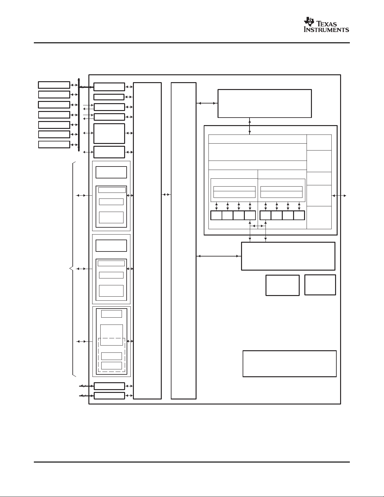
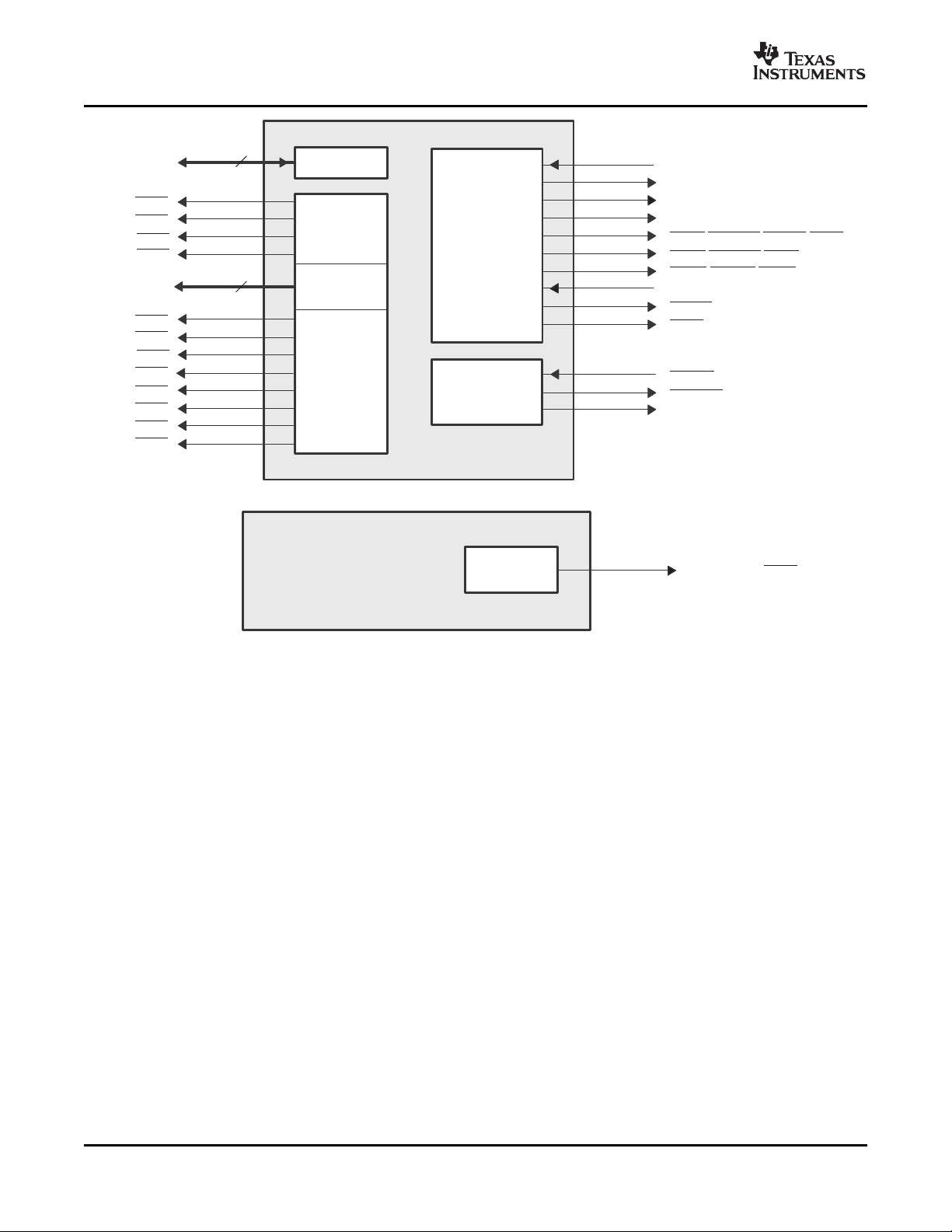
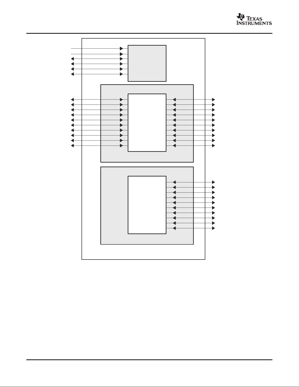
1.3 Functional Block Diagram
Figure 1-1 shows the functional block diagram of the DM642 device.
A. McBSPs: Framing Chips – H.100, MVIP, SCSA, T1, E1; AC97 Devices; SPI Devices; Codecs
B. The Video Port 0 (VP0) peripheral is muxed with the McBSP0 peripheral and the McASP0 control pins. The Video
Port 1 (VP1) peripheral is muxed with the McBSP1 peripheral and the McASP0 data pins. The PCI peripheral is
muxed with the HPI(32/16), EMAC, and MDIO peripherals. For more details on the multiplexed pins of these
peripherals, see the Device Configurations section of this data sheet.
Figure 1-1. Functional Block Diagram
TMS320DM642 Video/Imaging Fixed-Point Digital Signal Processor4 Submit Documentation Feedback

www.ti.com
TMS320DM642
Video/Imaging Fixed-Point Digital Signal Processor
SPRS200L – JULY 2002 – REVISED JANUARY 2007
Contents
1 TMS320DM642 Video/Imaging Fixed-Point Digital 5 DM642 Peripheral Information and Electrical
Signal Processor ......................................... 1 Specifications ........................................... 73
1.1 Features .............................................. 1 5.1 Parameter Information .............................. 73
1.2 Description ............................................ 2
1.2.1 Device Compatibility ................................. 3
1.3 Functional Block Diagram ............................ 4
2 Device Overview ......................................... 6
2.1 Device Characteristics ................................ 6
2.2 CPU (DSP Core) Description ......................... 7
2.3 Memory Map Summary ............................. 13
2.4 Bootmode ........................................... 16
2.5 Pin Assignments .................................... 16
2.6 Development ........................................ 50
3 Device Configurations ................................. 54
3.1 Configurations at Reset ............................. 54
3.2 Configurations After Reset .......................... 56
3.3 Peripheral Configuration Lock ....................... 59
3.4 Device Status Register Description ................. 61
3.5 Multiplexed Pin Configurations ...................... 63
3.6 Debugging Considerations .......................... 65
3.7 Configuration Examples ............................. 66
4 Device Operating Conditions ........................ 70
4.1 Absolute Maximum Ratings Over Operating Case
Temperature Range
(Unless Otherwise Noted) .......................... 70
4.2 Recommended Operating Conditions ............... 70
4.3 Electrical Characteristics Over Recommended
Ranges of Supply Voltage and Operating Case
Temperature (Unless Otherwise Noted) ............ 71
5.2 Recommended Clock and Control Signal Transition
Behavior ............................................. 75
5.3 Power Supplies ...................................... 75
5.4 Enhanced Direct Memory Access (EDMA)
Controller ............................................ 79
5.5 Interrupts ............................................ 83
5.6 Reset ................................................ 85
5.7 Clock PLL ........................................... 88
5.8 External Memory Interface (EMIF) .................. 94
5.9 Multichannel Audio Serial Port (McASP0)
Peripheral .......................................... 110
5.10 Inter-Integrated Circuit (I2C) ....................... 118
5.11 Host-Port Interface (HPI) ........................... 123
5.12 Peripheral Component Interconnect (PCI) ......... 129
5.13 Multichannel Buffered Serial Port (McBSP) ........ 133
5.14 Video Port .......................................... 142
5.15 VCXO Interpolated Control (VIC) .................. 150
5.16 Ethernet Media Access Controller (EMAC) ........ 152
5.17 Management Data Input/Output (MDIO) ........... 158
5.18 Timer ............................................... 160
5.19 General-Purpose Input/Output (GPIO) ............. 162
5.20 JTAG ............................................... 165
Revision History ............................................ 167
6 Mechanical Data ....................................... 168
6.1 Thermal Data ...................................... 168
6.2 Packaging Information ............................. 169
Submit Documentation Feedback Contents 5
www.ti.com
TMS320DM642
Video/Imaging Fixed-Point Digital Signal Processor
SPRS200L – JULY 2002 – REVISED JANUARY 2007
2 Device Overview
2.1 Device Characteristics
Table 2-1 provides an overview of the DM642 DSP. The table shows significant features of the DM642
device, including the capacity of on-chip RAM, the peripherals, the CPU frequency, and the package type
with pin count.
Table 2-1. Characteristics of the DM642 Processor
HARDWARE FEATURES DM642
EMIFA (64-bit bus width)
(clock source = AECLKIN)
EDMA (64 independent channels) 1
McASP0 (uses Peripheral Clock [AUXCLK]) 1
I2C0 (uses Peripheral Clock) 1
Peripherals
Not all peripherals pins are
available at the same time
(For more detail, see the
Device Configuration
section).
On-Chip Memory
CPU ID + CPU Rev ID Control Status Register (CSR.[31:16]) 0x0C01
JTAG BSDL_ID JTAGID register (address location: 0x01B3F008) 0x0007902F
Frequency MHz 500, 600, 720
Cycle Time ns
Voltage
PLL Options CLKIN frequency multiplier Bypass (x1), x6, x12
BGA Package
Process Technology µm 0.13 µm
Product Status
(1) On this DM64x™ device, the rated EMIF speed affects only the SDRAM interface on the EMIF. For more detailed information, see the
EMIF device speed portion of this data sheet.
(2) PRODUCTION DATA information is current as of publication date. Products conform to specifications per the terms of Texas
Instruments standard warranty. Production processing does not necessarily include testing of all parameters.
(2)
HPI (32- or 16-bit user selectable) 1 (HPI16 or HPI32)
PCI (32-bit), 66-MHz/33-MHz
[DeviceID Register value 0x9065]
McBSPs
(internal clock source = CPU/4 clock frequency)
Configurable Video Ports (VP0, VP1, VP2) 3
10/100 Ethernet MAC (EMAC) 1
Management Data Input/Output (MDIO) 1
VCXO Interpolated Control Port (VIC) 1
32-Bit Timers
(internal clock source = CPU/8 clock frequency)
General-Purpose Input/Output Port (GP0) 16
Size (Bytes) 288K
Organization 16KB L1 Data (L1D) Cache
Core (V)
I/O (V) 3.3 V
23 x 23 mm 548-Pin BGA (GDK and ZDK)
27 x 27 mm 548-Pin BGA (GNZ and ZNZ)
Product Preview (PP), Advance Information (AI),
or Production Data (PD)
16K-Byte (16KB) L1 Program (L1P) Cache
256KB Unified Mapped RAM/Cache (L2)
2 ns (DM642-500) and (DM642 A-500)
[500 MHz CPU, 100 MHz EMIF
1.67 ns (DM642-600) and (DM642 A-600)
[600 MHz CPU, 133 MHz EMIF
1.39 ns (DM642-720)
[720 MHz CPU, 133 MHz EMIF
1.4 V ( A-500, A-600, -600, -720)
1.2 V (–500)
1
1
2
3
(1)
, 33 MHz PCI port]
(1)
, 66 MHz PCI port]
(1)
, 66 MHz PCI port]
PD
Device Overview6 Submit Documentation Feedback

www.ti.com
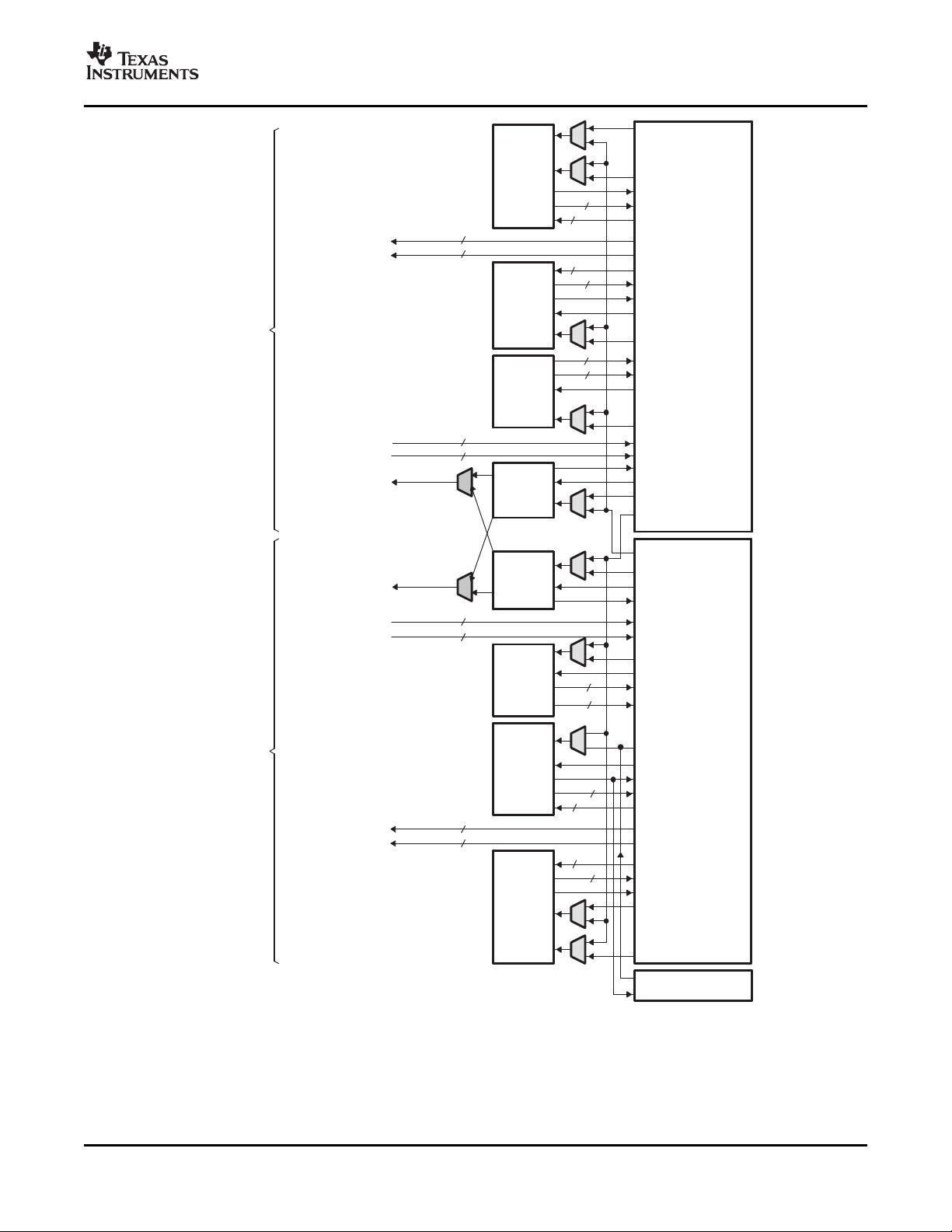
2.2 CPU (DSP Core) Description
The CPU fetches VelociTI™ advanced very-long instruction words (VLIWs) (256 bits wide) to supply up to
eight 32-bit instructions to the eight functional units during every clock cycle. The VelociTI™ VLIW
architecture features controls by which all eight units do not have to be supplied with instructions if they
are not ready to execute. The first bit of every 32-bit instruction determines if the next instruction belongs
to the same execute packet as the previous instruction, or whether it should be executed in the following
clock as a part of the next execute packet. Fetch packets are always 256 bits wide; however, the execute
packets can vary in size. The variable-length execute packets are a key memory-saving feature,
distinguishing the C64x CPUs from other VLIW architectures. The C64x™ VelociTI.2™ extensions add
enhancements to the TMS320C62x™ DSP VelociTI™ architecture. These enhancements include:
• Register file enhancements
• Data path extensions
• Quad 8-bit and dual 16-bit extensions with data flow enhancements
• Additional functional unit hardware
• Increased orthogonality of the instruction set
• Additional instructions that reduce code size and increase register flexibility
The CPU features two sets of functional units. Each set contains four units and a register file. One set
contains functional units .L1, .S1, .M1, and .D1; the other set contains units .D2, .M2, .S2, and .L2. The
two register files each contain 32 32-bit registers for a total of 64 general-purpose registers. In addition to
supporting the packed 16-bit and 32-/40-bit fixed-point data types found in the C62x™ VelociTI™ VLIW
architecture, the C64x™ register files also support packed 8-bit data and 64-bit fixed-point data types. The
two sets of functional units, along with two register files, compose sides A and B of the CPU [see the
functional block and CPU (DSP core) diagram, and Figure 2-1 ]. The four functional units on each side of
the CPU can freely share the 32 registers belonging to that side. Additionally, each side features a "data
cross path"—a single data bus connected to all the registers on the other side, by which the two sets of
functional units can access data from the register files on the opposite side. The C64x CPU pipelines
data-cross-path accesses over multiple clock cycles. This allows the same register to be used as a
data-cross-path operand by multiple functional units in the same execute packet. All functional units in the
C64x CPU can access operands via the data cross path. Register access by functional units on the same
side of the CPU as the register file can service all the units in a single clock cycle. On the C64x CPU, a
delay clock is introduced whenever an instruction attempts to read a register via a data cross path if that
register was updated in the previous clock cycle.
TMS320DM642
Video/Imaging Fixed-Point Digital Signal Processor
SPRS200L – JULY 2002 – REVISED JANUARY 2007
In addition to the C62x™ DSP fixed-point instructions, the C64x™ DSP includes a comprehensive
collection of quad 8-bit and dual 16-bit instruction set extensions. These VelociTI.2™ extensions allow the
C64x CPU to operate directly on packed data to streamline data flow and increase instruction set
efficiency. This is a key factor for video and imaging applications.
Another key feature of the C64x CPU is the load/store architecture, where all instructions operate on
registers (as opposed to data in memory). Two sets of data-addressing units (.D1 and .D2) are
responsible for all data transfers between the register files and the memory. The data address driven by
the .D units allows data addresses generated from one register file to be used to load or store data to or
from the other register file. The C64x .D units can load and store bytes (8 bits), half-words (16 bits), and
words (32 bits) with a single instruction. And with the new data path extensions, the C64x .D unit can load
and store doublewords (64 bits) with a single instruction. Furthermore, the non-aligned load and store
instructions allow the .D units to access words and doublewords on any byte boundary. The C64x CPU
supports a variety of indirect addressing modes using either linear- or circular-addressing with 5- or 15-bit
offsets. All instructions are conditional, and most can access any one of the 64 registers. Some registers,
however, are singled out to support specific addressing modes or to hold the condition for conditional
instructions (if the condition is not automatically "true").
Submit Documentation Feedback Device Overview 7

www.ti.com
TMS320DM642
Video/Imaging Fixed-Point Digital Signal Processor
SPRS200L – JULY 2002 – REVISED JANUARY 2007
The two .M functional units perform all multiplication operations. Each of the C64x .M units can perform
two 16 × 16-bit multiplies or four 8 × 8-bit multiplies per clock cycle. The .M unit can also perform 16 ×
32-bit multiply operations, dual 16 × 16-bit multiplies with add/subtract operations, and quad 8 × 8-bit
multiplies with add operations. In addition to standard multiplies, the C64x .M units include bit-count,
rotate, Galois field multiplies, and bidirectional variable shift hardware.
The two .S and .L functional units perform a general set of arithmetic, logical, and branch functions with
results available every clock cycle. The arithmetic and logical functions on the C64x CPU include single
32-bit, dual 16-bit, and quad 8-bit operations.
The processing flow begins when a 256-bit-wide instruction fetch packet is fetched from a program
memory. The 32-bit instructions destined for the individual functional units are "linked" together by "1" bits
in the least significant bit (LSB) position of the instructions. The instructions that are "chained" together for
simultaneous execution (up to eight in total) compose an execute packet. A "0" in the LSB of an
instruction breaks the chain, effectively placing the instructions that follow it in the next execute packet. A
C64x™ DSP device enhancement now allows execute packets to cross fetch-packet boundaries. In the
TMS320C62x™/TMS320C67x™ DSP devices, if an execute packet crosses the fetch-packet boundary
(256 bits wide), the assembler places it in the next fetch packet, while the remainder of the current fetch
packet is padded with NOP instructions. In the C64x™ DSP device, the execute boundary restrictions
have been removed, thereby, eliminating all of the NOPs added to pad the fetch packet, and thus,
decreasing the overall code size. The number of execute packets within a fetch packet can vary from one
to eight. Execute packets are dispatched to their respective functional units at the rate of one per clock
cycle and the next 256-bit fetch packet is not fetched until all the execute packets from the current fetch
packet have been dispatched. After decoding, the instructions simultaneously drive all active functional
units for a maximum execution rate of eight instructions every clock cycle. While most results are stored in
32-bit registers, they can be subsequently moved to memory as bytes, half-words, or doublewords. All
load and store instructions are byte-, half-word-, word-, or doubleword-addressable.
For more details on the C64x CPU functional units enhancements, see the following documents:
• TMS320C6000 CPU and Instruction Set Reference Guide (literature number SPRU189)
• TMS320C64x Technical Overview (literature number SPRU395)
Device Overview8 Submit Documentation Feedback
www.ti.com
.L1
.S1
.M1
.D1
.D2
.M2
.S2
.L2
src1
long dst
8
8
src2
DA1 (Address)
ST1b (Store Data)
ST2a (Store Data)
Register
File A
(A0−A31)
8
8
8
8
dst
Data Path A
DA2 (Address)
Register
File B
(B0− B31)
LD2a (Load Data)
Data Path B
Control Register
File
ST2b (Store Data)
LD1b (Load Data)
8
8
2X
1X
ST1a (Store Data)
(A)
LD1a (Load Data)
LD2b (Load Data)
32 MSBs
32 LSBs
32 MSBs
32 LSBs
32 MSBs
32 LSBs
32 MSBs
32 LSBs
src2
src1
dst
long dst
long src
long src
long dst
dst
src1
src2
src1
src2
src2
src1
dst
src2
src1
dst
src2
long dst
src2
src1
dst
long dst
long dst
long src
long src
long dst
dst
dst
src2
src1
dst
(A)
(A)
(A)
TMS320DM642
Video/Imaging Fixed-Point Digital Signal Processor
SPRS200L – JULY 2002 – REVISED JANUARY 2007
A. For the .M functional units, the long dst is 32 MSBs and the dst is 32 LSBs.
Submit Documentation Feedback Device Overview 9
Figure 2-1. TMS320C64x™ CPU (DSP Core) Data Paths
www.ti.com
TMS320DM642
Video/Imaging Fixed-Point Digital Signal Processor
SPRS200L – JULY 2002 – REVISED JANUARY 2007
2.2.1 CPU Core Registers
Table 2-2. L2 Cache Registers (C64x)
HEX ADDRESS RANGE ACRONYM REGISTER NAME COMMENTS
0184 0000 CCFG Cache configuration register
0184 0004 – 0184 0FFC – Reserved
0184 1000 EDMAWEIGHT L2 EDMA access control register
0184 1004 – 0184 1FFC – Reserved
0184 2000 L2ALLOC0 L2 allocation register 0
0184 2004 L2ALLOC1 L2 allocation register 1
0184 2008 L2ALLOC2 L2 allocation register 2
0184 200C L2ALLOC3 L2 allocation register 3
0184 2010 – 0184 3FFC – Reserved
0184 4000 L2WBAR L2 writeback base address register
0184 4004 L2WWC L2 writeback word count register
0184 4010 L2WIBAR L2 writeback invalidate base address register
0184 4014 L2WIWC L2 writeback invalidate word count register
0184 4018 L2IBAR L2 invalidate base address register
0184 401C L2IWC L2 invalidate word count register
0184 4020 L1PIBAR L1P invalidate base address register
0184 4024 L1PIWC L1P invalidate word count register
0184 4030 L1DWIBAR L1D writeback invalidate base address register
0184 4034 L1DWIWC L1D writeback invalidate word count register
0184 4038 – 0184 4044 – Reserved
0184 4048 L1DIBAR L1D invalidate base address register
0184 404C L1DIWC L1D invalidate word count register
0184 4050 – 0184 4FFC – Reserved
0184 5000 L2WB L2 writeback all register
0184 5004 L2WBINV L2 writeback invalidate all register
0184 5008 – 0184 7FFC – Reserved
0184 8000 – 0184 81FC Reserved
0184 8200 MAR128 Controls EMIFA CE0 range 8000 0000 – 80FF FFFF
0184 8204 MAR129 Controls EMIFA CE0 range 8100 0000 – 81FF FFFF
0184 8208 MAR130 Controls EMIFA CE0 range 8200 0000 – 82FF FFFF
0184 820C MAR131 Controls EMIFA CE0 range 8300 0000 – 83FF FFFF
0184 8210 MAR132 Controls EMIFA CE0 range 8400 0000 – 84FF FFFF
0184 8214 MAR133 Controls EMIFA CE0 range 8500 0000 – 85FF FFFF
0184 8218 MAR134 Controls EMIFA CE0 range 8600 0000 – 86FF FFFF
0184 821C MAR135 Controls EMIFA CE0 range 8700 0000 – 87FF FFFF
0184 8220 MAR136 Controls EMIFA CE0 range 8800 0000 – 88FF FFFF
0184 8224 MAR137 Controls EMIFA CE0 range 8900 0000 – 89FF FFFF
0184 8228 MAR138 Controls EMIFA CE0 range 8A00 0000 – 8AFF FFFF
0184 822C MAR139 Controls EMIFA CE0 range 8B00 0000 – 8BFF FFFF
0184 8230 MAR140 Controls EMIFA CE0 range 8C00 0000 – 8CFF FFFF
0184 8234 MAR141 Controls EMIFA CE0 range 8D00 0000 – 8DFF FFFF
0184 8238 MAR142 Controls EMIFA CE0 range 8E00 0000 – 8EFF FFFF
0184 823C MAR143 Controls EMIFA CE0 range 8F00 0000 – 8FFF FFFF
0184 8240 MAR144 Controls EMIFA CE1 range 9000 0000 – 90FF FFFF
MAR0 to
MAR127
Device Overview10 Submit Documentation Feedback
www.ti.com
Video/Imaging Fixed-Point Digital Signal Processor
SPRS200L – JULY 2002 – REVISED JANUARY 2007
Table 2-2. L2 Cache Registers (C64x) (continued)
HEX ADDRESS RANGE ACRONYM REGISTER NAME COMMENTS
0184 8244 MAR145 Controls EMIFA CE1 range 9100 0000 – 91FF FFFF
0184 8248 MAR146 Controls EMIFA CE1 range 9200 0000 – 92FF FFFF
0184 824C MAR147 Controls EMIFA CE1 range 9300 0000 – 93FF FFFF
0184 8250 MAR148 Controls EMIFA CE1 range 9400 0000 – 94FF FFFF
0184 8254 MAR149 Controls EMIFA CE1 range 9500 0000 – 95FF FFFF
0184 8258 MAR150 Controls EMIFA CE1 range 9600 0000 – 96FF FFFF
0184 825C MAR151 Controls EMIFA CE1 range 9700 0000 – 97FF FFFF
0184 8260 MAR152 Controls EMIFA CE1 range 9800 0000 – 98FF FFFF
0184 8264 MAR153 Controls EMIFA CE1 range 9900 0000 – 99FF FFFF
0184 8268 MAR154 Controls EMIFA CE1 range 9A00 0000 – 9AFF FFFF
0184 826C MAR155 Controls EMIFA CE1 range 9B00 0000 – 9BFF FFFF
0184 8270 MAR156 Controls EMIFA CE1 range 9C00 0000 – 9CFF FFFF
0184 8274 MAR157 Controls EMIFA CE1 range 9D00 0000 – 9DFF FFFF
0184 8278 MAR158 Controls EMIFA CE1 range 9E00 0000 – 9EFF FFFF
0184 827C MAR159 Controls EMIFA CE1 range 9F00 0000 – 9FFF FFFF
0184 8280 MAR160 Controls EMIFA CE2 range A000 0000 – A0FF FFFF
0184 8284 MAR161 Controls EMIFA CE2 range A100 0000 – A1FF FFFF
0184 8288 MAR162 Controls EMIFA CE2 range A200 0000 – A2FF FFFF
0184 828C MAR163 Controls EMIFA CE2 range A300 0000 – A3FF FFFF
0184 8290 MAR164 Controls EMIFA CE2 range A400 0000 – A4FF FFFF
0184 8294 MAR165 Controls EMIFA CE2 range A500 0000 – A5FF FFFF
0184 8298 MAR166 Controls EMIFA CE2 range A600 0000 – A6FF FFFF
0184 829C MAR167 Controls EMIFA CE2 range A700 0000 – A7FF FFFF
0184 82A0 MAR168 Controls EMIFA CE2 range A800 0000 – A8FF FFFF
0184 82A4 MAR169 Controls EMIFA CE2 range A900 0000 – A9FF FFFF
0184 82A8 MAR170 Controls EMIFA CE2 range AA00 0000 – AAFF FFFF
0184 82AC MAR171 Controls EMIFA CE2 range AB00 0000 – ABFF FFFF
0184 82B0 MAR172 Controls EMIFA CE2 range AC00 0000 – ACFF FFFF
0184 82B4 MAR173 Controls EMIFA CE2 range AD00 0000 – ADFF FFFF
0184 82B8 MAR174 Controls EMIFA CE2 range AE00 0000 – AEFF FFFF
0184 82BC MAR175 Controls EMIFA CE2 range AF00 0000 – AFFF FFFF
0184 82C0 MAR176 Controls EMIFA CE3 range B000 0000 – B0FF FFFF
0184 82C4 MAR177 Controls EMIFA CE3 range B100 0000 – B1FF FFFF
0184 82C8 MAR178 Controls EMIFA CE3 range B200 0000 – B2FF FFFF
0184 82CC MAR179 Controls EMIFA CE3 range B300 0000 – B3FF FFFF
0184 82D0 MAR180 Controls EMIFA CE3 range B400 0000 – B4FF FFFF
0184 82D4 MAR181 Controls EMIFA CE3 range B500 0000 – B5FF FFFF
0184 82D8 MAR182 Controls EMIFA CE3 range B600 0000 – B6FF FFFF
0184 82DC MAR183 Controls EMIFA CE3 range B700 0000 – B7FF FFFF
0184 82E0 MAR184 Controls EMIFA CE3 range B800 0000 – B8FF FFFF
0184 82E4 MAR185 Controls EMIFA CE3 range B900 0000 – B9FF FFFF
0184 82E8 MAR186 Controls EMIFA CE3 range BA00 0000 – BAFF FFFF
0184 82EC MAR187 Controls EMIFA CE3 range BB00 0000 – BBFF FFFF
0184 82F0 MAR188 Controls EMIFA CE3 range BC00 0000 – BCFF FFFF
0184 82F4 MAR189 Controls EMIFA CE3 range BD00 0000 – BDFF FFFF
0184 82F8 MAR190 Controls EMIFA CE3 range BE00 0000 – BEFF FFFF
0184 82FC MAR191 Controls EMIFA CE3 range BF00 0000 – BFFF FFFF
TMS320DM642
Submit Documentation Feedback Device Overview 11

www.ti.com
TMS320DM642
Video/Imaging Fixed-Point Digital Signal Processor
SPRS200L – JULY 2002 – REVISED JANUARY 2007
Table 2-2. L2 Cache Registers (C64x) (continued)
HEX ADDRESS RANGE ACRONYM REGISTER NAME COMMENTS
0184 8300 – 0184 83FC Reserved
0184 8400 – 0187 FFFF – Reserved
MAR192 to
MAR255
Device Overview12 Submit Documentation Feedback
www.ti.com
2.3 Memory Map Summary
Table 2-3 shows the memory map address ranges of the DM642 device. Internal memory is always
located at address 0 and can be used as both program and data memory. The external memory address
ranges in the DM642 device begin at the hex address location 0x8000 0000 for EMIFA.
TMS320DM642
Video/Imaging Fixed-Point Digital Signal Processor
SPRS200L – JULY 2002 – REVISED JANUARY 2007
Table 2-3. TMS320DM642 Memory Map Summary
MEMORY BLOCK DESCRIPTION HEX ADDRESS RANGE
Internal RAM (L2) 256K 0000 0000 – 0003 FFFF
Reserved 768K 0004 0000 – 000F FFFF
Reserved 23M 0010 0000 – 017F FFFF
External Memory Interface A (EMIFA) Registers 256K 0180 0000 – 0183 FFFF
L2 Registers 256K 0184 0000 – 0187 FFFF
HPI Registers 256K 0188 0000 – 018B FFFF
McBSP 0 Registers 256K 018C 0000 – 018F FFFF
McBSP 1 Registers 256K 0190 0000 – 0193 FFFF
Timer 0 Registers 256K 0194 0000 – 0197 FFFF
Timer 1 Registers 256K 0198 0000 – 019B FFFF
Interrupt Selector Registers 256K 019C 0000 – 019F FFFF
EDMA RAM and EDMA Registers 256K 01A0 0000 – 01A3 FFFF
Reserved 512K 01A4 0000 – 01AB FFFF
Timer 2 Registers 256K 01AC 0000 – 01AF FFFF
GP0 Registers 256K – 4K 01B0 0000 – 01B3 EFFF
Device Configuration Registers 4K 01B3 F000 – 01B3 FFFF
I2C0 Data and Control Registers 16K 01B4 0000 – 01B4 3FFF
Reserved 32K 01B4 4000 – 01B4 BFFF
McASP0 Control Registers 16K 01B4 C000 – 01B4 FFFF
Reserved 192K 01B5 0000 – 01B7 FFFF
Reserved 256K 01B8 0000 – 01BB FFFF
Emulation 256K 01BC 0000 – 01BF FFFF
PCI Registers 256K 01C0 0000 – 01C3 FFFF
VP0 Control 16K 01C4 0000 – 01C4 3FFF
VP1 Control 16K 01C4 4000 – 01C4 7FFF
VP2 Control 16K 01C4 8000 – 01C4 BFFF
VIC Control 16K 01C4 C000 – 01C4 FFFF
Reserved 192K 01C5 0000 – 01C7 FFFF
EMAC Control 4K 01C8 0000 – 01C8 0FFF
EMAC Wrapper 8K 01C8 1000 – 01C8 2FFF
EWRAP Registers 2K 01C8 3000 – 01C8 37FF
MDIO Control Registers 2K 01C8 3800 – 01C8 3FFF
Reserved 3.5M 01C8 4000 – 01FF FFFF
QDMA Registers 52 0200 0000 – 0200 0033
Reserved 736M – 52 0200 0034 – 2FFF FFFF
McBSP 0 Data 64M 3000 0000 – 33FF FFFF
McBSP 1 Data 64M 3400 0000 – 37FF FFFF
Reserved 64M 3800 0000 – 3BFF FFFF
McASP0 Data 1M 3C00 0000 – 3C0F FFFF
Reserved 64M – 1M 3C10 0000 – 3FFF FFFF
Reserved 832M 4000 0000 – 73FF FFFF
BLOCK SIZE
(BYTES)
Submit Documentation Feedback Device Overview 13
www.ti.com
TMS320DM642
Video/Imaging Fixed-Point Digital Signal Processor
SPRS200L – JULY 2002 – REVISED JANUARY 2007
Table 2-3. TMS320DM642 Memory Map Summary (continued)
MEMORY BLOCK DESCRIPTION HEX ADDRESS RANGE
VP0 Channel A Data 32M 7400 0000 – 75FF FFFF
VP0 Channel B Data 32M 7600 0000 – 77FF FFFF
VP1 Channel A Data 32M 7800 0000 – 79FF FFFF
VP1 Channel B Data 32M 7A00 0000 – 7BFF FFFF
VP2 Channel A Data 32M 7C00 0000 – 7DFF FFFF
VP2 Channel B Data 32M 7E00 0000 – 7FFF FFFF
EMIFA CE0 256M 8000 0000 – 8FFF FFFF
EMIFA CE1 256M 9000 0000 – 9FFF FFFF
EMIFA CE2 256M A000 0000 – AFFF FFFF
EMIFA CE3 256M B000 0000 – BFFF FFFF
Reserved 1G C000 0000 – FFFF FFFF
BLOCK SIZE
(BYTES)
Device Overview14 Submit Documentation Feedback
www.ti.com
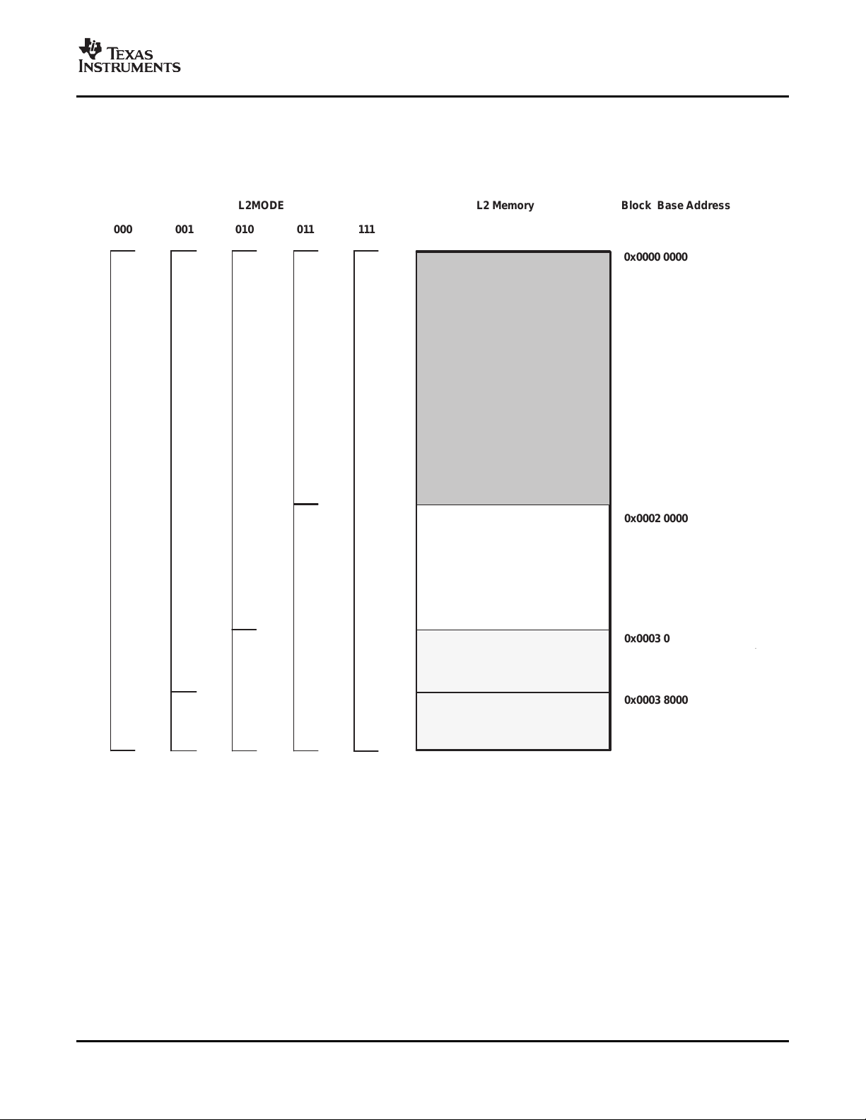
2.3.1 L2 Architecture Expanded
0x0000 0000
011010001 111
0x0002 0000
000
L2MODE L2 Memory Block Base Address
0x0003 8000
0x0003 0000
0x0004 0000
32K Cache
(4 Way)
64K Cache (4 Way)
128K Cache (4 Way)
256K Cache (4 Way) [All]
256K SRAM (All)
224K SRAM
192K SRAM
128K SRAM
128K-Byte SRAM
64K-Byte RAM
32K-Byte RAM
0x0003 FFFF
32K-Byte RAM
Figure 2-2 shows the detail of the L2 architecture on the TMS320DM642 device. For more information on
the L2MODE bits, see the cache configuration (CCFG) register bit field descriptions in the TMS320C64x
Two-Level Internal Memory Reference Guide (literature number SPRU610).
TMS320DM642
Video/Imaging Fixed-Point Digital Signal Processor
SPRS200L – JULY 2002 – REVISED JANUARY 2007
Figure 2-2. TMS320DM642 L2 Architecture Memory Configuration
Submit Documentation Feedback Device Overview 15

www.ti.com
TMS320DM642
Video/Imaging Fixed-Point Digital Signal Processor
SPRS200L – JULY 2002 – REVISED JANUARY 2007
2.4 Bootmode
The DM642 device resets using the active-low signal RESET. While RESET is low, the device is held in
reset and is initialized to the prescribed reset state. Refer to reset timing for reset timing characteristics
and states of device pins during reset. The release of RESET starts the processor running with the
prescribed device configuration and boot mode.
The DM642 has three types of boot modes:
• Host boot
If host boot is selected, upon release of RESET, the CPU is internally "stalled" while the remainder of
the device is released. During this period, an external host can initialize the CPU's memory space as
necessary through the host interface, including internal configuration registers, such as those that
control the EMIF or other peripherals. For the DM642 device, the HPI peripheral is used for host boot if
PCI_EN = 0, and the PCI peripheral is used if PCI_EN = 1. Once the host is finished with all necessary
initialization, it must set the DSPINT bit in the HPIC register to complete the boot process. This
transition causes the boot configuration logic to bring the CPU out of the "stalled" state. The CPU then
begins execution from address 0. The DSPINT condition is not latched by the CPU, because it occurs
while the CPU is still internally "stalled". Also, DSPINT brings the CPU out of the "stalled" state only if
the host boot process is selected. All memory may be written to and read by the host. This allows for
the host to verify what it sends to the DSP if required. After the CPU is out of the "stalled" state, the
CPU needs to clear the DSPINT, otherwise, no more DSPINTs can be received.
• EMIF boot (using default ROM timings)
Upon the release of RESET, the 1K-Byte ROM code located in the beginning of CE1 is copied to
address 0 by the EDMA using the default ROM timings, while the CPU is internally "stalled". The data
should be stored in the endian format that the system is using. In this case, the EMIF automatically
assembles consecutive 8-bit bytes to form the 32-bit instruction words to be copied. The transfer is
automatically done by the EDMA as a single-frame block transfer from the ROM to address 0. After
completion of the block transfer, the CPU is released from the "stalled" state and starts running from
address 0.
• No boot
With no boot, the CPU begins direct execution from the memory located at address 0. Note: operation
is undefined if invalid code is located at address 0.
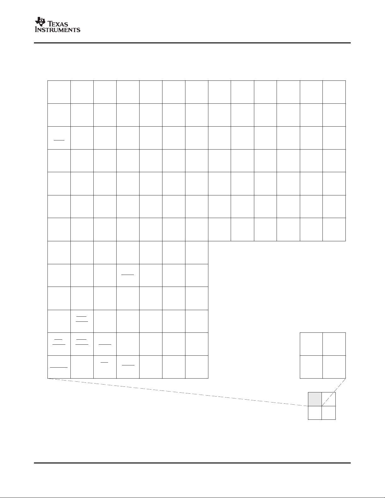
2.5 Pin Assignments
16 Device Overview Submit Documentation Feedback
www.ti.com
2.5.1 Pin Map
AF
AE
AD
AC
AB
AA
Y
W
V
U
T
R
P
13121110987654321
13121110987654321
CLKMODE1
CLKMODE0
PLLV
RESET
VDAC/
GP0[8]/
PCI66
HCNTL1/
PDEVSEL
HCS/
PPERR
HAS/
PPAR
HDS1/
PSERR
HDS2/
PCBE1
HD15/
AD15
HD14/
AD14
HD13/
AD13
HD12/
AD12
HD11/
AD11
HD10/
AD10
HD9/
AD9
HD8/
AD8
HD7/
AD7
HD6/
AD6
HD4/
AD4
HD3/
AD3
HD2/
AD2
HD1/
AD1
HD0/
AD0
PCBE0
XSP_CS
XSP_CLK/
MDCLK
XSP_DI
XSP_DO/
MDIO
STCLK
VP1D[18]/
AXR0[6]
VP1D[19]/
AXR0[7]
VP1D[15]/
AXR0[3]
VP1D[17]/
AXR0[5]
VP0D[19]/
AHCLKX0
VP1D[16]/
AXR0[4]
VP1D[14]/
AXR0[2]
VP1D[13]/
AXR0[1]
VP1D[12]/
AXR0[0]
VP1D[11]
VP1D[10]
VP1D[9]
VP1D[8]/
CLKR1
VP1D[7]/
FSR1
VP1D[6]/
DR1
VP1D[5]/
CLKS1
VP1D[4]/
DX1
VP1D[3]/
FSX1
VP1D[2]/
CLKX1
VP1D[1]
VP1D[0] VP1CLK1VP1CLK0
VP1CTL2
VP1CTL1
VP1CTL0
VP0D[17]/
ACLKX0
VP0D[16]/
AMUTE0
VP0D[15]/
AMUTEIN0
VP0CLK1
VP0D[18]/
AFSX0
RSV
RSV
RSV
RSV
RSV
RSV
RSV
DV
DD
DV
DD
DV
DD
DV
DD
DV
DD
DV
DD
DV
DD
DV
DD
DV
DD
DV
DD
DV
DD
DV
DD
DV
DD
CV
DD
CV
DD
CV
DD
CV
DD
CV
DD
CV
DD
CV
DD
CV
DD
CV
DD
CV
DD
CV
DD
CV
DD
CV
DD
V
SS
V
SS
V
SS
V
SS
V
SS
V
SS
V
SS
V
SS
CLKIN V
SS
V
SS
V
SS
V
SS
V
SS
V
SS
V
SS
V
SS
V
SS
V
SS
V
SS
V
SS
V
SS
V
SS
V
SS
V
SS
V
SS
V
SS
V
SS
V
SS
V
SS
V
SS
V
SS
V
SS
V
SS
V
SS
V
SS
VSSV
SS
V
SS
V
SS
HD5/
AD5
HCNTL0/
PSTOP
V
SS
TMS320DM642
Video/Imaging Fixed-Point Digital Signal Processor
SPRS200L – JULY 2002 – REVISED JANUARY 2007
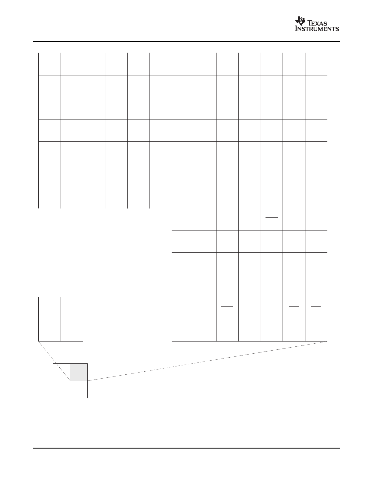
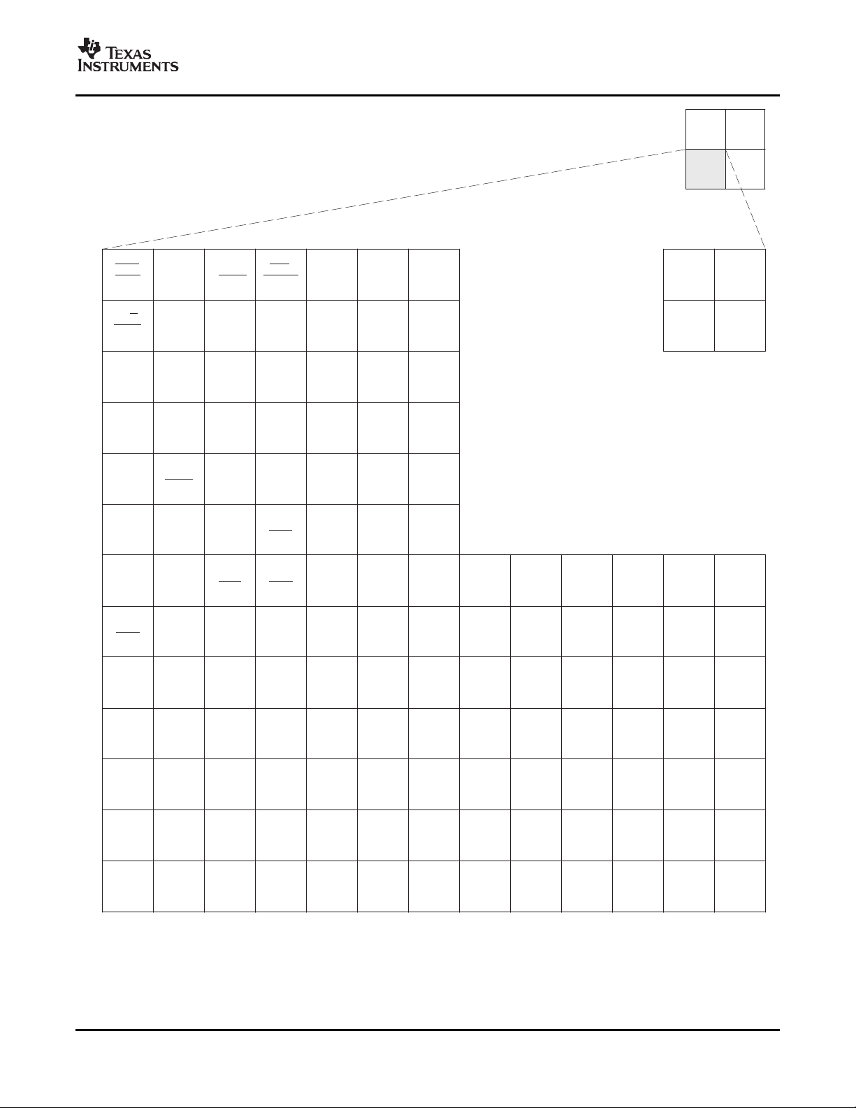
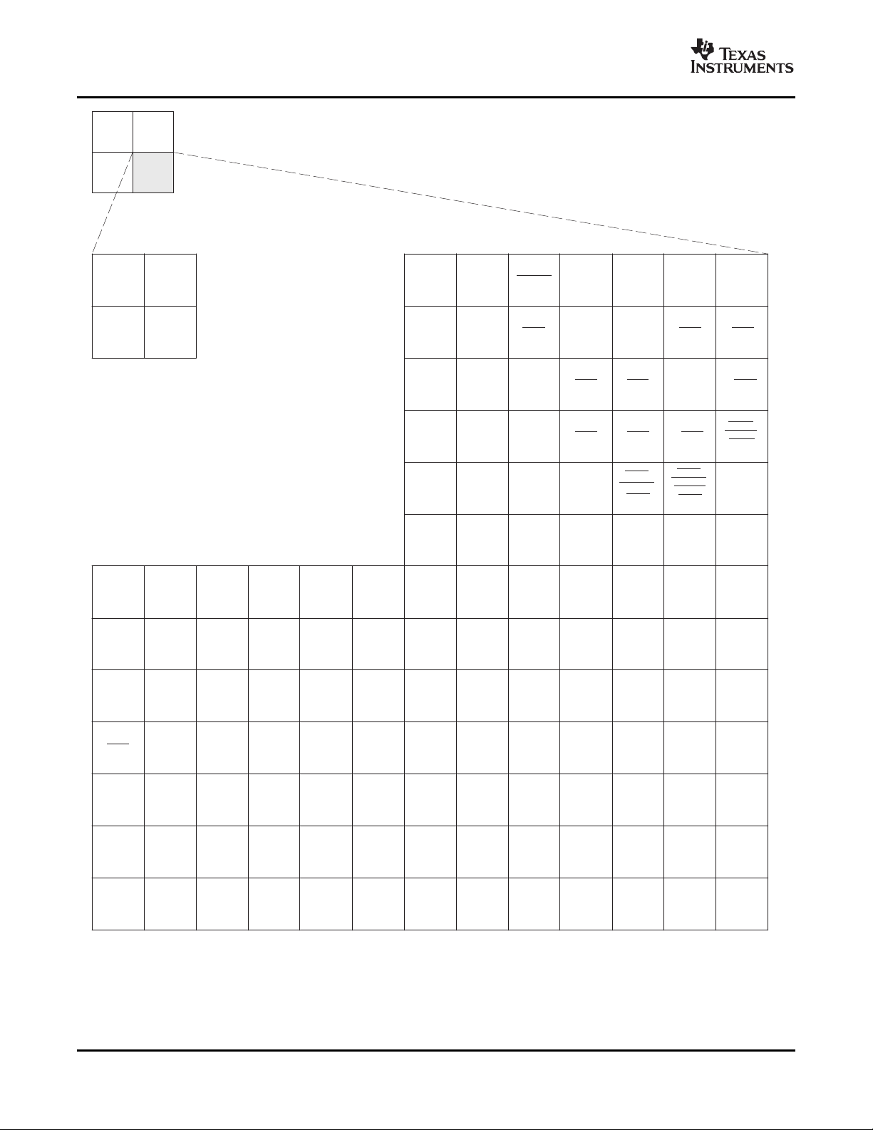
Figure 2-3 through Figure 2-6 show the DM642 pin assignments in four quadrants (A, B, C, and D).
Figure 2-3. DM642 Pin Map [Quadrant A]
Submit Documentation Feedback Device Overview 17
www.ti.com
14 15 16 17 18 19 20 21 22 23 24 25 26
AF
AE
AD
AC
AB
AA
Y
W
V
U
T
R
P
ABE7 ABE6
ABE5 ABE4
ABUSREQ
ASOE3
AEA22
AEA21 AEA20 AEA19AEA18
AEA17 AEA16 AEA15
AEA14 AEA13
AEA12 AEA11
AEA10 AEA9 AEA8
AED63AED62
AED61
AED60AED59
AED58AED58
AED57
AED56
AED55
AED54
AED53
AED52
AED51
AED50
AED49
AED48
AED47
AED46AED45 AED44AED43
AED42AED41 AED40AED39
AED38 AED37AED36
AED35AED34
AED33 AED32
VP0D[14]/
AHCLKR0
VP0D[13]/
AFSR0
VP0D[12]/
ACLKR0
VP0D[11]
VP0D[10]
VP0D[9]
VP0D[8]/
CLKR0
VP0D[7]/
FSR0
VP0D[6]/
DR0
VP0D[5]/
CLKS0
VP0D[4]/
DX0
VP0D[3]/
FSX0
VP0D[2]/
CLKX0
VP0D[1]
VP0D[0]VP0D[0]VP0CLK0
VP0CTL2
VP0CTL1
VP0CTL0
DV
DD
DV
DD
DV
DD
DVDDDV
DD
AHOLDDV
DD
DV
DD
DV
DD
DV
DD
DV
DD
DV
DD
DV
DD
DVDDDV
DD
DV
DD
DV
DD
DV
DD
DV
DD
DV
DD
DV
DD
CV
DD
CV
DD
CV
DD
CV
DD
CV
DD
CV
DD
CV
DD
CV
DD
CV
DD
CV
DD
CV
DD
CV
DD
CV
DD
V
SS
V
SS
V
SS
V
SS
V
SS
V
SS
V
SS
V
SS
V
SS
V
SS
V
SS
V
SS
V
SS
VSSV
SS
V
SS
V
SS
V
SS
V
SS
V
SS
V
SS
V
SS
V
SS
V
SS
V
SS
V
SS
V
SS
V
SS
V
SS
V
SS
V
SS
V
SS
V
SS
CV
DD
14 15 16 17 18 19 20 21 22 23 24 25 26
TMS320DM642
Video/Imaging Fixed-Point Digital Signal Processor
SPRS200L – JULY 2002 – REVISED JANUARY 2007
Figure 2-4. DM642 Pin Map [Quadrant B]
Device Overview18 Submit Documentation Feedback
www.ti.com
N
M
L
K
J
H
G
F
E
D
C
B
A
CLKOUT6/
GP0[2]
NMI
GP0[7]/
EXT_INT7
GP0[6]/
EXT_INT6
GP0[5]/
EXT_INT5
GP0[4]/
EXT_INT4
GP0[15]/
PRST
GP0[14]/
PCLK
GP0[13]/
PINTA
GP0[12]/
PGNT
GP0[11]/
PREQ
GP0[10]/
PCBE3
GP0[9]/
PIDSEL
GP0[3]/
PCIEEAI
GP0[0]
PCI_EN
HINT/
PFRAME
HHWIL/
PTRDY
HR/W/
PCBE2
HRDY/
PIRDY
HD31/
AD31/
MRCLK
HD30/
AD30/
MCRS
HD29/
AD29/
MRXER
HD28/
AD28/
MRXDV
HD27/
AD27/
MRXD3
HD26/
AD26/
MRXD2
HD25/
AD25/
MRXD1
HD24/
AD24/
MRXD0
HD23/
AD23
13121110987654321
HD22/
AD22/
MTCLK
HD21/
AD21/
MCOL
HD20/
AD20/
MTXEN
HD19/
AD19/
MTXD3
HD18/
AD18/
MTXD2
HD17/
AD17/
MTXD1
HD16/
AD16/
MTXD0
VP2D[19]VP2D[18]
VP2D[16]
VP2D[15]
VP2D[14]
VP2D[12]
VP2D[10]
VP2D[8]
VP2D[6]
VP2D[4]VP2D[4]
VP2D[2]
VP2D[0]
VP2CLK0 VP2CLK1
VP2CTL2
TOUT1/
LENDIAN
TINP1
TOUT0/
MAC_EN
TINP0
SCL0
RSV
DV
DD
DV
DD
DV
DD
DV
DD
DV
DD
DV
DD
DV
DD
DV
DD
DV
DD
DV
DD
DVDDDV
DD
DV
DD
DV
DD
DV
DD
DV
DD
DV
DD
CV
DD
CV
DD
CV
DD
CV
DD
CV
DD
CV
DD
CV
DD
CV
DD
CV
DD
CV
DD
CV
DD
CV
DD
CV
DD
V
SS
V
SS
V
SS
V
SS
V
SS
V
SS
V
SS
V
SS
V
SS
V
SS
V
SS
V
SS
V
SS
V
SS
V
SS
V
SS
V
SS
V
SS
V
SS
V
SS
V
SS
V
SS
V
SS
VSSV
SS
V
SS
V
SS
V
SS
V
SS
V
SS
V
SS
V
SS
V
SS
V
SS
V
SS
V
SS
V
SS
V
SS
V
SS
SDA0 DV
DD
CLKOUT4/
GP0[1]
VP2CTL1 VP2D[1] VP2D[5] VP2D[9] VP2D[13] VP2D[17]
VP2CTL0 VP2D[3] VP2D[7] VP2D[11]
13121110987654321
Video/Imaging Fixed-Point Digital Signal Processor
SPRS200L – JULY 2002 – REVISED JANUARY 2007
TMS320DM642
Figure 2-5. DM642 Pin Map [Quadrant C]
Submit Documentation Feedback Device Overview 19
www.ti.com
N
M
L
K
J
H
G
F
E
D
C
B
A
14 15 16 17 18 19 20 21 22 23 24 25 26
14 15 16 17 18 19 20 21 22 23 24 25 26
TMS
TDO
TDITCK
TRST EMU11
EMU10
EMU9
EMU8
EMU7
EMU6
EMU5
EMU4
EMU3
EMU2
EMU1
EMU0
ACE3
ACE2 ACE1 ACE0
ABE3 ABE2
ABE1 ABE0
APDT
AHOLDA
AECLKIN
AAOE/
ASDRAS/
ASOE
AARDY
AECLKOUT1
AARE/
ASDCAS/
ASADS/
ASRE
AAWE/
ASDWE/
ASWE
ASDCKE
AEA7 AEA6 AEA5
AEA4AEA4 AEA3
AED31AED30
AED29AED28
AED27 AED26
AED25 AED24AED23 AED22
AED21 AED20AED19 AED18
AED17 AED16
AED15
AED14
AED13
AED12
AED11
AED10
AED9
AED8
AED7
AED6 AED4
AED3
AED5
AED2
AED1
AED0
RSV
DV
DD
V
SS
V
SS
DV
DD
DV
DD
DV
DD
DV
DD
DV
DD
V
SS
DV
DD
DV
DD
DV
DD
DV
DD
DV
DD
DV
DD
DV
DD
DV
DD
DV
DD
DVDDDV
DD
DV
DD
CV
DD
CV
DD
CV
DD
CV
DD
CV
DD
CV
DD
CV
DD
CV
DD
CV
DD
CV
DD
CV
DD
CV
DD
CV
DD
V
SS
V
SS
V
SS
V
SS
V
SS
V
SS
V
SS
V
SS
V
SS
V
SS
V
SS
V
SS
V
SS
V
SS
V
SS
V
SS
V
SS
V
SS
V
SS
V
SS
V
SS
V
SS
V
SS
V
SS
V
SS
V
SS
V
SS
V
SS
V
SS
V
SS
AECLKOUT2
CV
DD
TMS320DM642
Video/Imaging Fixed-Point Digital Signal Processor
SPRS200L – JULY 2002 – REVISED JANUARY 2007
Figure 2-6. DM642 Pin Map [Quadrant D]
20 Device Overview Submit Documentation Feedback

www.ti.com
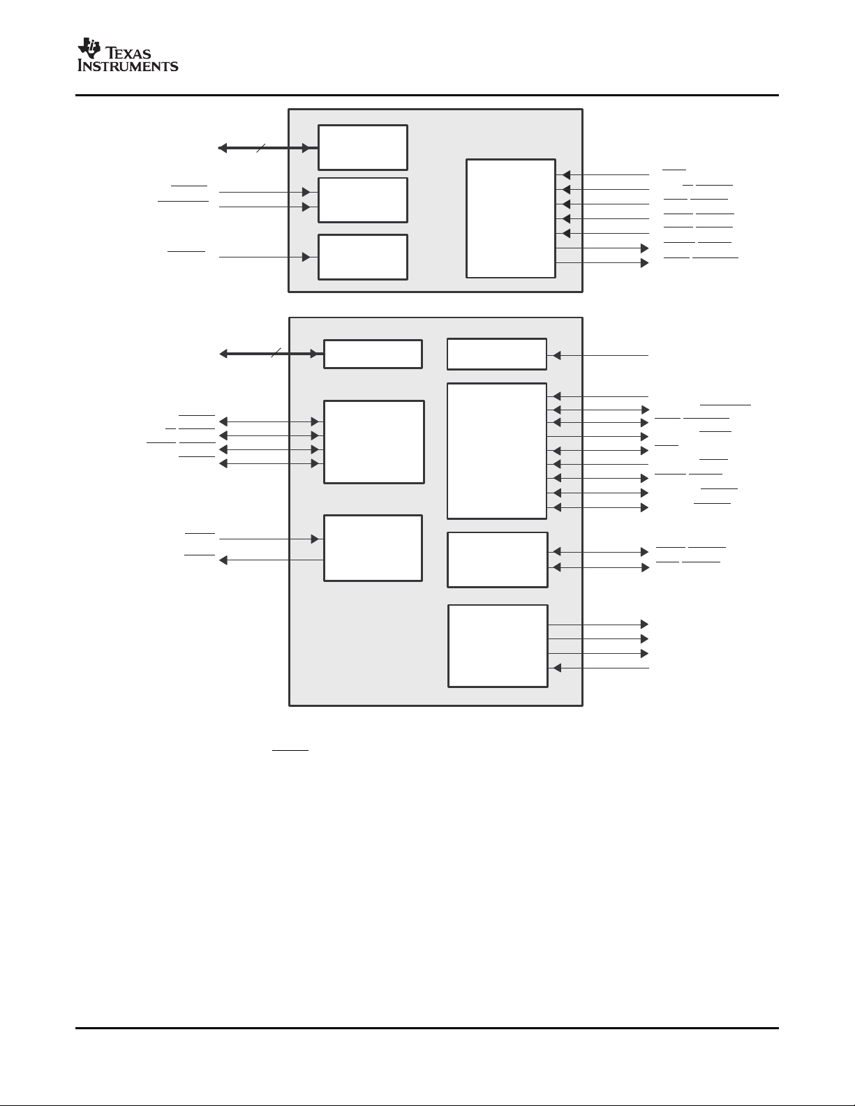
2.5.2 Signal Groups Description
TRST
GP0[7]/EXT_INT7
(B)
IEEE Standard
1149.1
(JTAG)
Emulation
Reserved
Reset and
Interrupts
Control/Status
TDI
TDO
TMS
TCK
EMU0
EMU1
NMI
GP0[6]/EXT_INT6
(B)
GP0[5]/EXT_INT5
(B)
GP0[4]/EXT_INT4
(B)
RESET
RSV07
RSV06
Clock/PLL
CLKIN
CLKMODE1
CLKMODE0
PLLV
EMU2
EMU3
EMU4
EMU5
GP0
General-Purpose Input/Output 0 (GP0) Port
GP0[7]/EXT_INT7
(B)
GP0[6]/EXT_INT6
(B)
GP0[5]/EXT_INT5
(B)
GP0[4]/EXT_INT4
(B)
GP0[3]/PCIEEAI
CLKOUT6/GP0[2]
(A)
CLKOUT4/GP0[1]
(A)
GP0[0]
CLKOUT6/GP0[2]
(A)
CLKOUT4/GP0[1]
(A)
EMU6
EMU7
EMU8
EMU9
EMU10
GP0[15]/PRST
(C)
GP0[14]/PCLK
(C)
GP0[13]/PINTA
(C)
GP0[12]/PGNT
(C)
GP0[11]/PREQ
(C)
GP0[10]/PCBE3
(C)
GP0[9]/PIDSEL
(C)
VDAC/GP0[8]/PCI66
(C)
RSV08
EMU11
RSV04
RSV03
RSV05
Peripheral
Control/Status
PCI_EN
TOUT0/MAC_EN
RSV01
RSV00
RSV02
TMS320DM642
Video/Imaging Fixed-Point Digital Signal Processor
SPRS200L – JULY 2002 – REVISED JANUARY 2007
Submit Documentation Feedback Device Overview 21
A. These pins are muxed with the GP0 pins and by default these signals function as clocks (CLKOUT4 or CLKOUT6).
To use these muxed pins as GPIO signals, the appropriate GPIO register bits (GPxEN and GPxDIR) must be properly
enabled and configured. For more details, see the Device Configurations section of this data sheet.
B. These pins are GP0 pins that can also function as external interrupt sources (EXT_INT[7:4]). Default after reset is
EXT_INTx or GPIO as input-only.
C. These GP0 pins are muxed with the PCI peripheral pins and by default these signals are set up to no function with
both the GPIO and PCI pin functions disabled. For more details on these muxed pins, see the Device Configurations
section of this data sheet.
Figure 2-7. CPU and Peripheral Signals
www.ti.com
ACE3
AECLKOUT1
AED[63:0]
ACE2
ACE1
ACE0
AEA[22:3]
ABE7
ABE6
ABE5
ABE4
AARDY
Data
Memory Map
Space Select
Address
Byte Enables
64
20
External
Memory I/F
Control
EMIFA (64-bit)
AECLKIN
AHOLD
AHOLDA
ABUSREQ
Bus
Arbitration
AARE/ASDCAS/ASADS/ASRE
ASDCKE
AECLKOUT2
ASOE3
ABE3
ABE2
ABE1
ABE0
AAOE/ASDRAS/ASOE
AAWE/ASDWE/ASWE
APDT
VDAC/GP0[8]/PCI66
VCXO Interpolated
Control Port (VIC)
Data
TMS320DM642
Video/Imaging Fixed-Point Digital Signal Processor
SPRS200L – JULY 2002 – REVISED JANUARY 2007
Figure 2-8. EMIFA/VIC Peripheral Signals
Device Overview22 Submit Documentation Feedback
www.ti.com
HHWIL/PTRDY
HCNTL0/PSTOP
HCNTL1/PDEVSEL
Data
Register Select
Half-Word
Select
Control
HPI
(A)
(Host-Port Interface)
32
HD[15:0]/AD[15:0]
HAS/PPAR
HR/W/PCBE2
HCS/PPERR
HDS1/PSERR
HDS2/PCBE1
HRDY/PIRDY
HINT/PFRAME
(HPI16 ONL Y)
HD[15:0]/AD[15:0]
HR/W/PCBE2
HDS2/PCBE1
PCBE0
GP0[12]/PGNT
GP0[11]/PREQ
GP0[14]/PCLK
HINT/PFRAME
GP0[13]/PINTA
Data/Address
Arbitration
32
Clock
Control
PCI Interface
(B)
HAS/PPAR
GP0[15]/PRST
HRDY/PIRDY
HCNTL0/PSTOP
HHWIL/PTRDY
GP0[10]/PCBE3
GP0[9]/PIDSEL
HCNTL1/PDEVSEL
HDS1/PSERR
Error
Command
Byte Enable
Serial
EEPROM
XSP_DO/MDIO
XSP_CS
XSP_CLK/MDCLK
XSP_DI
HCS/PPERR
HD[31:16]/AD[31:16]
(C)
HD[31:16]/AD[31:16]
(C)
Video/Imaging Fixed-Point Digital Signal Processor
SPRS200L – JULY 2002 – REVISED JANUARY 2007
TMS320DM642
A. These HPI pins are muxed with the PCI peripheral. By default, these signals function as HPI. For more details on
these muxed pins, see the Device Configurations section of this data sheet.
B. These PCI pins (excluding PCBE0 and XSP_CS) are muxed with the HPI or MDIO or GP0 peripherals. By default,
these signals function as HPI and no function, respectively. For more details on these muxed pins, see the Device
Configurations section of this data sheet.
C. These HPI/PCI data pins (HD[31:16/AD[31:16]) are muxed with the EMAC peripheral. By default, these pins function
as HPI. For more details on the EMAC pin functions, see the Ethernet MAC (EMAC) peripheral signals section and
the terminal functions table portions of this data sheet.
Figure 2-9. HPI/PCI Peripheral Signals
Submit Documentation Feedback Device Overview 23
www.ti.com
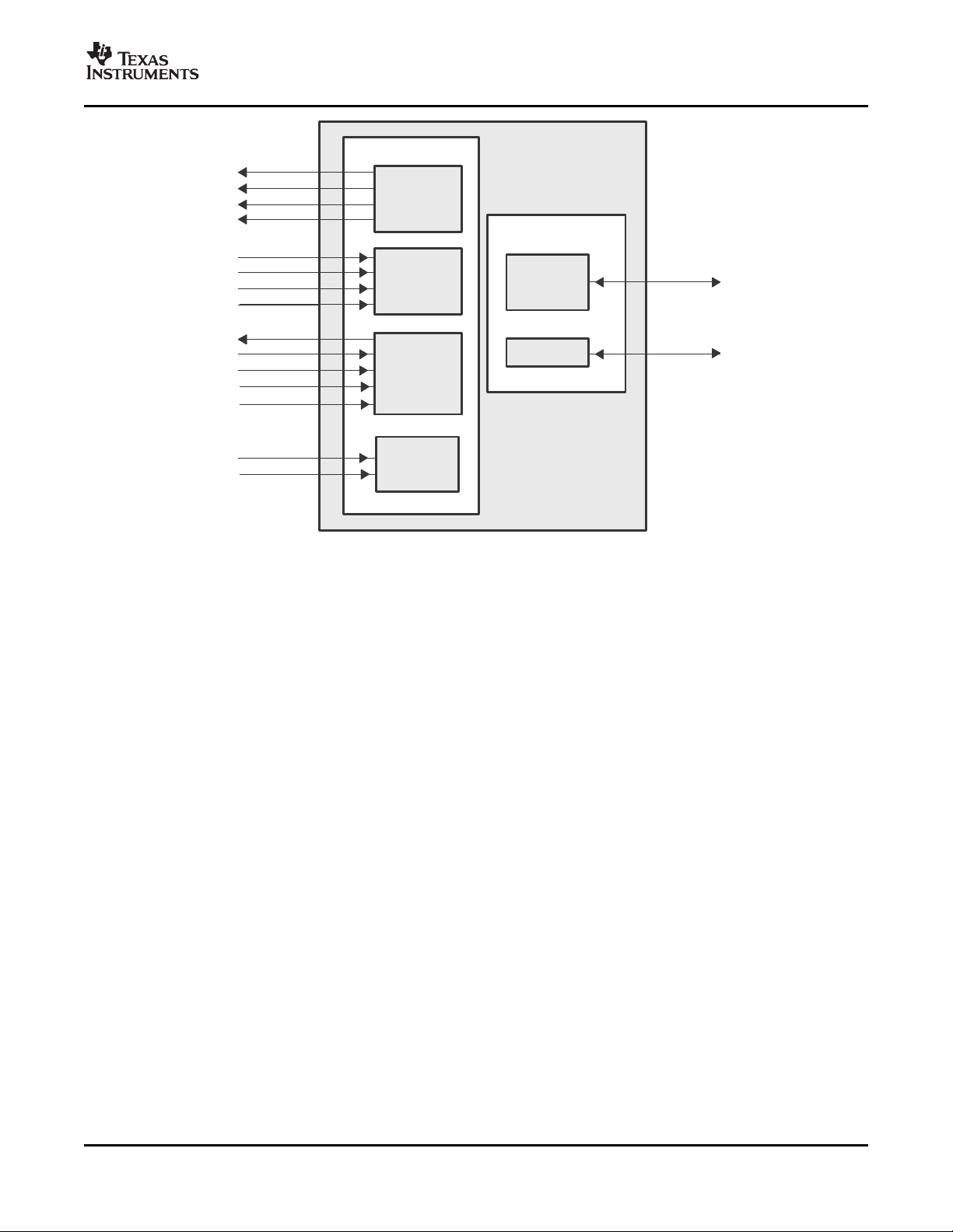
McBSPs
(Multichannel Buffered
Serial Ports)
VP0D[2]/CLKX0
(A)
VP0D[3]/FSX0
(A)
VP0D[4]/DX0
(A)
VP0D[8]/CLKR0
(A)
VP0D[7]/FSR0
(A)
VP0D[6]/DR0
(A)
VP0D[5]/CLKS0
(A)
McBSP0
VP1D[2]/CLKX1
(A)
VP1D[3]/FSX1
(A)
VP1D[4]/DX1
(A)
VP1D[8]/CLKR1
(A)
VP1D[7]/FSR1
(A)
VP1D[6]/DR1
(A)
VP1D[5]/CLKS1
(A)
McBSP1
TOUT0/MACEN
Timers
TINP0
TOUT1/LENDIAN
Timer 1
TINP1
Timer 2
Timer 0
SCL0
I2C0
I2C0
SDA0
Transmit
Receive
Clock
Transmit
Receive
Clock
TMS320DM642
Video/Imaging Fixed-Point Digital Signal Processor
SPRS200L – JULY 2002 – REVISED JANUARY 2007
A. These McBSP1 and McBSP0 pins are muxed with the Video Port 1 (VP1) and Video Port 0 (VP0) peripherals,
respectively. By default, these signals function as VP1 and VP0, respectively. For more details on these muxed pins,
see the Device Configurations section of this data sheet.
Figure 2-10. McBSP/Timer/I2C0 Peripheral Signals
Device Overview24 Submit Documentation Feedback
www.ti.com
HD21/AD21/MCOL
(A)
HD28/AD28/MRXDV
(A)
HD29/AD29/MRXER
(A)
HD20/AD20/MTXEN
(A)
Ethernet MAC (EMAC)
and MDIO
XSP_DO/MDIO
(B)
XSP_CLK/MDCLK
(B)
MDIO
Clock
HD16/AD16/MTXD0
(A)
HD17/AD17/MTXD1
(A)
HD18/AD18/MTXD2
(A)
HD25/AD25/MRXD1
(A)
HD26/AD26/MRXD2
(A)
HD27/AD27/MRXD3
(A)
EMAC
Transmit
HD24/AD24/MRXD0
(A)
HD19/AD19/MTXD3
(A)
Clocks
HD31/AD31/MRCLK
(A)
HD22/AD22/MTCLK
(A)
HD30/AD30/MCRS
(A)
Error Detect
and Control
Input/Output
Receive
Video/Imaging Fixed-Point Digital Signal Processor
SPRS200L – JULY 2002 – REVISED JANUARY 2007
TMS320DM642
A. These EMAC pins are muxed with the upper data pins of the HPI or PCI peripherals. By default, these signals
function as HPI. For more details on these muxed pins, see the Device Configurations section of this data sheet.
B. These MDIO pins are muxed with the PCI peripherals. By default, these signals function as PCI. For more details on
these muxed pins, see the Device Configurations section of this data sheet.
Figure 2-11. EMAC/MDIO Peripheral Signals
Submit Documentation Feedback Device Overview 25
www.ti.com
VP0D[10]
VP0D[11]
VP0D[12]/ACLKR0
VP0D[13]/AFSR0
VP0D[14]/AHCLKR0
VP0D[15]/AMUTEIN0
VP0D[16]/AMUTE0
VP0D[17]/ACLKX0
VP0D[0]
VP0D[1]
VP0D[2]/CLKX0
VP0D[3]/FSX0
VP0D[4]/DX0
VP0D[5]/CLKS0
VP0D[6]/DR0
VP0D[7]/FSR0
VP0D[8]/CLKR0
VP0D[9]
VP0D[18]/AFSX0
VP0D[19]/AHCLKX0
Capture/Display
Buffer
(2560 Bytes)
VP0CLK0
VP0CLK1
VP0CTL0
VP0CTL1
VP0CTL2
Timing and
Control Logic
Video Port 0 (VP0)
Channel B
(B)
Channel A
(A)
Capture/Display
Buffer
(2560 Bytes)
Channel B uses only
the VP0D[19:10]
bidirectional pins
STCLK
(C)
TMS320DM642
Video/Imaging Fixed-Point Digital Signal Processor
SPRS200L – JULY 2002 – REVISED JANUARY 2007
A. Channel A supports: BT.656 (8/10-bit), Y/C Video (16/20-bit), RAW Video (16/20-bit) display modes and BT.656
(8/10-bit), Y/C Video (16/20-bit), RAW Video (16/20-bit), and TSI (8-bit) capture modes.
B. Channel B supports: BT.656 (8/10-bit), RAW Video (8/10-bit) capture modes and can display synchronized RAW
Video data with Channel A.
C. The same STCLK signal is used for all three video ports (VP0, VP1, and VP2).
Figure 2-12. Video Port 0 Peripheral Signals
Device Overview26 Submit Documentation Feedback
www.ti.com
VP1D[10]
VP1D[11]
VP1D[12]/AXR0[0]
VP1D[13]/AXR0[1]
VP1D[14]/AXR0[2]
VP1D[15]/AXR0[3]
VP1D[16]/AXR0[4]
VP1D[17]/AXR0[5]
VP1D[0]
VP1D[1]
VP1D[2]/CLKX1
VP1D[3]/FSX1
VP1D[4]/DX1
VP1D[5]/CLKS1
VP1D[6]/DR1
VP1D[7]/FSR1
VP1D[8]/CLKR1
VP1D[9]
VP1D[18]/AXR0[6]
VP1D[19]/AXR0[7]
Capture/Display
Buffer
(2560 Bytes)
VP1CLK0
VP1CLK1
VP1CTL0
VP1CTL1
VP1CTL2
Timing and
Control Logic
Video Port 1 (VP1)
Channel B
(B)
Channel A
(A)
Capture/Display
Buffer
(2560 Bytes)
Channel B uses only
the VP1D[19:10]
bidirectional pins
STCLK
(C)
Video/Imaging Fixed-Point Digital Signal Processor
SPRS200L – JULY 2002 – REVISED JANUARY 2007
TMS320DM642
A. Channel A supports: BT.656 (8/10-bit), Y/C Video (16/20-bit), RAW Video (16/20-bit) display modes and BT.656
(8/10-bit), Y/C Video (16/20-bit), RAW Video (16/20-bit), and TSI (8-bit) capture modes.
B. Channel B supports: BT.656 (8/10-bit), RAW Video (8/10-bit) capture modes and can display synchronized RAW
Video data with Channel A.
C. The same STCLK signal is used for all three video ports (VP0, VP1, and VP2).
Figure 2-13. Video Port 1 Peripheral Signals
Submit Documentation Feedback Device Overview 27
www.ti.com
VP2D[10]
VP2D[11]
VP2D[12]
VP2D[13]
VP2D[14]
VP2D[15]
VP2D[16]
VP2D[17]
VP2D[0]
VP2D[1]
VP2D[2]
VP2D[3]
VP2D[4]
VP2D[5]
VP2D[6]
VP2D[7]
VP2D[8]
VP2D[9]
VP2D[18]
VP2D[19]
Capture/Display
Buffer
(2560 Bytes)
VP2CLK0
VP2CLK1
VP2CTL0
VP2CTL1
VP2CTL2
Timing and
Control Logic
Video Port 2 (VP2)
Channel B
(B)
Channel A
(A)
Capture/Display
Buffer
(2560 Bytes)
Channel B uses only
the VP2D[19:10]
bidirectional pins
STCLK
(C)
TMS320DM642
Video/Imaging Fixed-Point Digital Signal Processor
SPRS200L – JULY 2002 – REVISED JANUARY 2007
A. Channel A supports: BT.656 (8/10-bit), Y/C Video (16/20-bit), RAW Video (16/20-bit) display modes and BT.656
(8/10-bit), Y/C Video (16/20-bit), RAW Video (16/20-bit) and TSI (8-bit) capture modes.
B. Channel B supports: BT.656 (8/10-bit), RAW Video (8/10-bit) capture modes and can display synchronized RAW
Video data with Channel A.
C. The same STCLK signal is used for all three video ports (VP0, VP1, and VP2).
Figure 2-14. Video Port 2 Peripheral Signals
Device Overview28 Submit Documentation Feedback

www.ti.com
VP1D[19]/AXR0[7]
McASP0
(Multichannel Audio Serial Port 0)
VP1D[18]/AXR0[6]
VP0D[17]/ACLKX0
VP0D[19]/AHCLKX0
Transmit
Clock
Generator
VP0D[15]/AMUTEIN0
Auto Mute
Logic
VP0D[16]/AMUTE0
VP0D[18]/AFSX0
Transmit
Frame Sync
VP0D[13]/AFSR0
Receive Frame
Sync
VP1D[17]/AXR0[5]
VP1D[16]/AXR0[4]
VP0D[12]/ACLKR0
VP0D[14]/AHCLKR0
Receive Clock
Generator
VP1D[15]/AXR0[3]
VP1D[14]/AXR0[2]
VP1D[13]/AXR0[1]
VP1D[12]/AXR0[0]
8-Serial Ports
Flexible
Partitioning
Tx, Rx, OFF
Transmit
Clock Check
Circuit
Receive Clock
Check Circuit
Error Detect
(A)
(Transmit/Receive Data Pins)(Transmit/Receive Data Pins)
(Receive Bit Clock)
(Transmit Bit Clock)
(Receive Master Clock) (Transmit Master Clock)
(Receive Frame Sync or
Left/Right Clock)
(Transmit Frame Sync or
Left/Right Clock)
NOTES: On multiplexed pins, bolded text denotes the active function of the pin for that particular peripheral module.
Bolded and Italicized text within parentheses denotes the function of the pins in an audio system.
Video/Imaging Fixed-Point Digital Signal Processor
SPRS200L – JULY 2002 – REVISED JANUARY 2007
TMS320DM642
A. The McASPs' Error Detect function detects underruns, overruns, early/late frame syncs, DMA errors, and external
mute input.
Figure 2-15. McASP0 Peripheral Signals
2.5.3 Terminal Functions
Table 2-4 , the terminal functions table, identifies the external signal names, the associated pin (ball)
numbers along with the mechanical package designator, the pin type (I, O/Z, or I/O/Z), whether the pin
has any internal pullup/pulldown resistors and a functional pin description. For more detailed information
on device configuration, peripheral selection, multiplexed/shared pins, and debugging considerations, see
the Device Configurations section of this data sheet.
Submit Documentation Feedback Device Overview 29

www.ti.com
TMS320DM642
Video/Imaging Fixed-Point Digital Signal Processor
SPRS200L – JULY 2002 – REVISED JANUARY 2007
Table 2-4. Terminal Functions
SIGNAL
NAME NO.
TYPE
IPD/
(1)
(2)
IPU
DESCRIPTION
CLOCK/PLL CONFIGURATION
CLKIN AC2 I Clock Input. This clock is the input to the on-chip PLL.
CLKOUT4/GP0[1]
CLKOUT6/GP0[2]
(3)
(3)
D6 I/O/Z IPU
C6 I/O/Z IPU
Clock output at 1/4 of the device speed ( O/Z) [default] or this pin can be
programmed as a GP0 1 pin ( I/O/Z).
Clock output at 1/6 of the device speed ( O/Z) [default] or this pin can be
programmed as a GP0 2 pin ( I/O/Z).
CLKMODE1 AE4 I IPD Clock mode select
• Selects whether the CPU clock frequency = input clock frequency x1
CLKMODE0 AA2 I IPD
(Bypass), x6, or x12.
For more details on the CLKMODE pins and the PLL multiply factors, see
the Clock PLL section of this data sheet.
(4)
PLLV
V6 A
(1)
PLL voltage supply
JTAG EMULATION
TMS E15 I IPU JTAG test-port mode select
TDO B18 O/Z IPU JTAG test-port data out
TDI A18 I IPU JTAG test-port data in
TCK A16 I IPU JTAG test-port clock
TRST D14 I IPD
JTAG test-port reset. For IEEE 1149.1 JTAG compatibility, see the IEEE 1149.1
JTAG compatibility statement portion of this data sheet.
EMU11 D17 I/O/Z IPU Emulation pin 11. Reserved for future use, leave unconnected.
EMU10 C17 I/O/Z IPU Emulation pin 10. Reserved for future use, leave unconnected.
EMU9 B17 I/O/Z IPU Emulation pin 9. Reserved for future use, leave unconnected.
EMU8 D16 I/O/Z IPU Emulation pin 8. Reserved for future use, leave unconnected.
EMU7 A17 I/O/Z IPU Emulation pin 7. Reserved for future use, leave unconnected.
EMU6 C16 I/O/Z IPU Emulation pin 6. Reserved for future use, leave unconnected.
EMU5 B16 I/O/Z IPU Emulation pin 5. Reserved for future use, leave unconnected.
EMU4 D15 I/O/Z IPU Emulation pin 4. Reserved for future use, leave unconnected.
EMU3 C15 I/O/Z IPU Emulation pin 3. Reserved for future use, leave unconnected.
EMU2 B15 I/O/Z IPU Emulation pin 2. Reserved for future use, leave unconnected.
EMU1 C14 I/O/Z IPU Emulation pin 1
EMU0 A15 I/O/Z IPU Emulation pin 0
(5)
(5)
RESETS, INTERRUPTS, AND GENERAL-PURPOSE INPUT/OUTPUTS
RESET P4 I Device reset
Nonmaskable interrupt, edge-driven (rising edge)
NMI B4 I IPD
Note: Any noise on the NMI pin may trigger an NMI interrupt; therefore, if the
NMI pin is not used, it is recommended that the NMI pin be grounded versus
relying on the IPD.
GP0[7]/EXT_INT7 E1 I/O/Z IPU General-purpose input/output (GPIO) pins ( I/O/Z) or external interrupts ( input
GP0[6]/EXT_INT6 F2 I/O/Z IPU
GP0[5]/EXT_INT5 F3 I/O/Z IPU
GP0[4]/EXT_INT4 F4 I/O/Z IPU
only). The default after reset setting is GPIO enabled as input-only.
• When these pins function as External Interrupts [by selecting the
corresponding interrupt enable register bit (IER.[7:4])], they are edge-driven
and the polarity can be independently selected via the External Interrupt
Polarity Register bits (EXTPOL.[3:0]).
(1) I = Input, O = Output, Z = High impedance, S = Supply voltage, GND = Ground, A = Analog signal
(2) IPD = Internal pulldown, IPU = Internal pullup. (These IPD/IPU signal pins feature a 30-k Ω IPD or IPU resistor. To pull up a signal to the
opposite supply rail, a 1-k Ω resistor should be used.)
(3) These pins are multiplexed pins. For more details, see the Device Configurations section of this data sheet.
(4) PLLV is not part of external voltage supply. See the Clock PLL section for information on how to connect this pin.
(5) The EMU0 and EMU1 pins are internally pulled up with 30-k Ω resistors; therefore, for emulation and normal operation, no external
pullup/pulldown resistors are necessary. However, for boundary scan operation, pull down the EMU1 and EMU0 pins with a dedicated
1-k Ω resistor.
Device Overview30 Submit Documentation Feedback
www.ti.com
TMS320DM642
Video/Imaging Fixed-Point Digital Signal Processor
SPRS200L – JULY 2002 – REVISED JANUARY 2007
Table 2-4. Terminal Functions (continued)
GP0[15]/ PRST
GP0[14]/PCLK
GP0[13]/ PINTA
GP0[12]/ PGNT
GP0[11]/ PREQ
GP0[10]/ PCBE3
GP0[9]/PIDSEL
SIGNAL
NAME NO.
(3)
(3)
(3)
(3)
(3)
(3)
(3)
G3
C1
G4
H4
TYPE
F1
J2
I/O/Z
K3
GP0[3] L5 IPD
GP0[0] M5 I/O/Z IPD
VDAC/GP0[8]/ PCI66
CLKOUT6/GP0[2]
CLKOUT4/GP0[1]
(3)
AD1 I/O/Z IPD
(3)
(3)
C6 I/O/Z IPU
D6 I/O/Z IPU
HOST-PORT INTERFACE (HPI) or PERIPHERAL COMPONENT INTERCONNECT (PCI) or EMAC
PCI_EN E2 I IPD the HPI, EMAC, MDIO, and GP0[15:8], or PCI peripherals. The pins work in
HINT/ PFRAME
HCNTL1/ PDEVSEL
HCNTL0/ PSTOP
HHWIL/ PTRDY
HR/ W/ PCBE2
HAS/PPAR
HCS/ PPERR
HDS1/ PSERR
HDS2/ PCBE1
HRDY/ PIRDY
(3)
(3)
(3)
(3)
(3)
(3)
(3)
(3)
(3)
(3)
N4 I/O/Z Host interrupt from DSP to host ( O) [default] or PCI frame ( I/O/Z)
P1 I/O/Z
R3 I/O/Z
N3 I/O/Z order)
M1 I/O/Z Host read or write select ( I) [default] or PCI command/byte enable 2 ( I/O/Z)
P3 I/O/Z Host address strobe ( I) [default] or PCI parity ( I/O/Z)
R1 I/O/Z
R2 I/O/Z
T2 I/O/Z
N1 I/O/Z Host ready from DSP to host ( O) [default] or PCI initiator ready ( I/O/Z).
IPD/
(1)
(2)
IPU
DESCRIPTION
General-purpose input/output (GP0) 15 pin ( I/O/Z) or PCI reset ( I).
GP0 14 pin ( I/O/Z) or PCI clock ( I)
GP0 13 pin ( I/O/Z) or PCI interrupt A ( O/Z)
GP0 12 pin ( I/O/Z) or PCI bus grant ( I)
GP0 11 pin ( I/O/Z) or PCI bus request ( O/Z)
GP0 10 pin ( I/O/Z) or PCI command/byte enable 3 ( I/O/Z)
GP0 9 pin ( I/O/Z) or PCI initialization device select ( I)
Note: By default, no function is enabled upon reset. To configure these pins, see
the Device Configuration section of this data sheet.
GP0 3 pin ( I/O/Z)
Boot Configuration: PCI EEPROM Auto-Initialization (EEAI).
0 - PCI auto-initialization through EEPROM is disabled (default).
1 - PCI auto-initialization through EEPROM is enabled.
General-purpose 0 pin (GP0[0]) ( I/O/Z) [default]
This pin can be programmed as GPIO 0 ( input only) [default] or as GP0[0]
( output only) pin or output as a general-purpose interrupt (GP0INT) signal
( output only).
Note: This pin must remain low during device reset.
VCXO Interpolated Control Port (VIC) single-bit digital-to-analog converter
(VDAC) output [ output only] [default] or this pin can be programmed as a GP0 8
pin ( I/O/Z)
Boot Configuration: PCI frequency selection ( PCI66).
If the PCI peripheral is enabled (PCI_EN pin = 1), then:
0 - PCI operates at 66 MHz (default).
1 - PCI operates at 33 MHz.
The –500 device supports PCI at 33 MHz only. For proper –500 device operation
when the PCI peripheral is enabled (PCI_EN = 1), this pin must be pulled up
with a 1-k Ω resistor at device reset.
Note: If the PCI peripheral is disabled (PCI_EN pin = 0), this pin be must not
pulled up.
Clock output at 1/6 of the device speed ( O/Z) [default] or this pin can be
programmed as a GP0 2 pin ( I/O/Z).
Clock output at 1/4 of the device speed ( O/Z) [default] or this pin can be
programmed as a GP0 1 pin ( I/O/Z).
Boot Configuration: PCI enable pin ( I)
The PCI_EN pin and the MAC_EN pin control the selection (enable/disable) of
conjunction to enable/disable these peripherals (for more details, see the Device
Configurations section of this data sheet).
Host control – selects between control, address, or data registers ( I) [default] or
PCI device select ( I/O/Z).
Host control – selects between control, address, or data registers ( I) [default] or
PCI stop ( I/O/Z)
Host half-word select – first or second half-word (not necessarily high or low
[For HPI16 bus width selection only] ( I) [default] or PCI target ready ( I/O/Z)
Host chip select ( I) [default] or PCI parity error ( I/O/Z)
Host data strobe 1 ( I) [default] or PCI system error ( I/O/Z)
Host data strobe 2 ( I) [default] or PCI command/byte enable 1 ( I/O/Z)
Note: If unused, the following HPI control signals should be externally pulled
high.
Submit Documentation Feedback Device Overview 31

www.ti.com
TMS320DM642
Video/Imaging Fixed-Point Digital Signal Processor
SPRS200L – JULY 2002 – REVISED JANUARY 2007
Table 2-4. Terminal Functions (continued)
SIGNAL
NAME NO.
HD31/AD31/MRCLK
HD30/AD30/MCRS
HD29/AD29/MRXER
HD28/AD28/MRXDV
HD27/AD27/MRXD3
HD26/AD26/MRXD2
HD25/AD25/MRXD1
HD24/AD24/MRXD0
HD23/AD23
(3)
HD22/AD22/MTCLK
HD21/AD21/MCOL
HD20/AD20/MTXEN
HD19/AD19/MTXD3
HD18/AD18/MTXD2
HD17/AD17/MTXD1
HD16/AD16/MTXD0
HD15/AD15
HD14/AD14
HD13/AD13
HD12/AD12
HD11/AD11
HD10/AD10
HD9/AD9
HD8/AD8
HD7/AD7
HD6/AD6
HD5/AD5
HD4/AD4
HD3/AD3
HD2/AD2
HD1/AD1
HD0/AD0
(3)
(3)
(3)
(3)
(3)
(3)
(3)
(3)
(3)
(3)
(3)
(3)
(3)
(3)
(3)
(3)
(3)
G1
(3)
(3)
H3
(3)
G2
(3)
(3)
H2
(3)
(3)
(3)
(3)
(3)
(3)
(3)
M4
(3)
M2
(3)
M3
U1
U3
U2
U4
W2
W4
W3
AA1
PCBE0 V4 I/O/Z
XSP_CS T4 O IPD
XSP_CLK/MDCLK
(3)
R5 I/O/Z IPD PCI serial interface clock ( O) [default] or MDIO serial clock input/output ( I/O/Z).
XSP_DI R4 I IPU
XSP_DO/MDIO
(3)
TYPE
J4
J3
J1
K4
K1
L4
K2
L3
L2
T3
I/O/Z
V1
V3
V2
Y1
Y2
Y4
Y3
P5 I/O/Z IPU ( I/O/Z). In PCI mode, this pin is connected to the input data pin of the serial
IPD/
(1)
(2)
IPU
DESCRIPTION
Host-port data ( I/O/Z) [default] or PCI data-address bus ( I/O/Z) or EMAC
transmit/receive or control pins
As HPI data bus (PCI_EN pin = 0)
• Used for transfer of data, address, and control
• Host-Port bus width user-configurable at device reset via a 10-k Ω resistor
pullup/pulldown resistor on the HD5 pin:
As PCI data-address bus (PCI_EN pin = 1)
• Used for transfer of data and address
Boot Configuration:
• HD5 pin = 0: HPI operates as an HPI16.
(HPI bus is 16 bits wide. HD[15:0] pins are used and the remaining
HD[31:16] pins are reserved pins in the high-impedance state.)
• HD5 pin = 1: HPI operates as an HPI32.
(HPI bus is 32 bits wide. All HD[31:0] pins are used for host-port operations.)
For superset devices like DM642, the HD31/AD31 through HD16/AD16 pins can
also function as EMAC transmit/receive or control pins (when PCI_EN pin = 0;
MAC_EN pin = 1). For more details on the EMAC pin functions, see the Ethernet
MAC (EMAC) peripheral section of this table and for more details on how to
configure the EMAC pin functions, see the device configuration section of this
data sheet.
PCI command/byte enable 0 ( I/O/Z).
When PCI is disabled (PCI_EN = 0), this pin is tied-off.
PCI serial interface chip select ( O).
When PCI is disabled (PCI_EN = 0), this pin is tied-off.
PCI serial interface data in ( I) [default].
In PCI mode, this pin is connected to the output data pin of the serial PROM.
PCI serial interface data out ( O) [default] or MDIO serial data input/output
PROM.
Device Overview32 Submit Documentation Feedback

www.ti.com
Video/Imaging Fixed-Point Digital Signal Processor
Table 2-4. Terminal Functions (continued)
GP0[15]/ PRST
GP0[14]/PCLK
GP0[13]/ PINTA
GP0[12]/ PGNT
GP0[11]/ PREQ
GP0[10]/ PCBE3
GP0[9]/PIDSEL
SIGNAL
NAME NO.
(3)
(3)
(3)
(3)
(3)
(3)
(3)
G3
C1
G4
H4 I/O/Z
TYPE
F1
J2
K3
GP0[3] L5 I/O/Z IPD
VDAC/GP0[8]/ PCI66
(3)
AD1 I/O/Z IPD
EMIFA (64-bit) – CONTROL SIGNALS COMMON TO ALL TYPES OF MEMORY
ACE3 L26 O/Z IPU
ACE2 K23 O/Z IPU
ACE1 K24 O/Z IPU
ACE0 K25 O/Z IPU
ABE7 T22 O/Z IPU
ABE6 T23 O/Z IPU
ABE5 R25 O/Z IPU
ABE4 R26 O/Z IPU
ABE3 M25 O/Z IPU
ABE2 M26 O/Z IPU
ABE1 L23 O/Z IPU
ABE0 L24 O/Z IPU
APDT M22 O/Z IPU
AHOLDA N22 O IPU EMIFA hold-request-acknowledge to the host
AHOLD W24 I IPU EMIFA hold request from the host
ABUSREQ P22 O IPU EMIFA bus request output
IPD/
(1)
(2)
IPU
DESCRIPTION
General-purpose input/output (GP0) 15 pin ( I/O/Z) or PCI reset ( I).
GP0 14 pin ( I/O/Z) or PCI clock ( I)
GP0 13 pin ( I/O/Z) or PCI interrupt A ( O/Z)
GP0 12 pin ( I/O/Z) or PCI bus grant ( I)
GP0 11 pin ( I/O/Z) or PCI bus request ( O/Z)
GP0 10 pin ( I/O/Z) or PCI command/byte enable 3 ( I/O/Z)
GP0 9 pin ( I/O/Z) or PCI initialization device select ( I)
Note: By default, no function is enabled upon reset. To configure these pins, see
the Device Configuration section of this data sheet.
GP0 3 pin ( I/O/Z)
Boot Configuration: PCI EEPROM Auto-Initialization (EEAI).
0 - PCI auto-initialization through EEPROM is disabled (default).
1 - PCI auto-initialization through EEPROM is enabled
VCXO Interpolated Control Port (VIC) single-bit digital-to-analog converter
(VDAC) output [ output only] [default] or this pin can be programmed as a GP0 8
pin ( I/O/Z)
Boot Configuration: PCI frequency selection ( PCI66).
If the PCI peripheral is enabled (PCI_EN pin = 1), then:
0 - PCI operates at 66 MHz (default).
1 - PCI operates at 33 MHz.
The –500 device supports PCI at 33 MHz only. For proper –500 device operation
when the PCI peripheral is enabled (PCI_EN = 1), this pin must be pulled up
with a 1-k Ω resistor at device reset.
Note: If the PCI peripheral is disabled (PCI_EN pin = 0), this pin must not be
pulled up.
EMIFA memory space enables
• Enabled by bits 28 through 31 of the word address
• Only one pin is asserted during any external data access
EMIFA byte-enable control
• Decoded from the low-order address bits. The number of address bits or
byte enables used depends on the width of external memory.
• Byte-write enables for most types of memory
• Can be directly connected to SDRAM read and write mask signal (SDQM)
EMIFA peripheral data transfer, allows direct transfer between external
peripherals
EMIFA (64-bit) – BUS ARBITRATION
TMS320DM642
SPRS200L – JULY 2002 – REVISED JANUARY 2007
Submit Documentation Feedback Device Overview 33

www.ti.com
TMS320DM642
Video/Imaging Fixed-Point Digital Signal Processor
SPRS200L – JULY 2002 – REVISED JANUARY 2007
Table 2-4. Terminal Functions (continued)
SIGNAL
NAME NO.
AECLKIN H25 I IPD
AECLKOUT2 J23 O/Z IPD
AECLKOUT1 J26 O/Z IPD
AARE/
ASDCAS/ J25 O/Z IPU
ASADS/ ASRE
AAOE/
ASDRAS/ J24 O/Z IPU
ASOE
AAWE/
ASDWE/ K26 O/Z IPU
ASWE
ASDCKE L25 O/Z IPU
ASOE3 R22 O/Z IPU
AARDY L22 I IPU Asynchronous memory ready input
AEA22 U23
AEA21 V24
AEA20 V25
AEA19 V26
AEA18 V23
AEA17 U24
AEA16 U25
AEA15 U26
AEA14 T24
AEA13 T25
AEA12 R23
AEA11 R24
AEA10 P23
AEA9 P24
AEA8 P26
AEA7 N23
AEA6 N24
AEA5 N26
AEA4 M23
AEA3 M24
TYPE
EMIFA (64-bit) – ASYNCHRONOUS/SYNCHRONOUS MEMORY CONTROL
O/Z IPD
IPD/
(1)
(2)
IPU
EMIFA external input clock. The EMIFA input clock (AECLKIN, CPU/4 clock, or
CPU/6 clock) is selected at reset via the pullup/pulldown resistors on the
AEA[20:19] pins.
AECLKIN is the default for the EMIFA input clock.
EMIFA output clock 2. Programmable to be EMIFA input clock (AECLKIN,
CPU/4 clock, or CPU/6 clock) frequency divided-by-1, -2, or -4.
EMIFA output clock 1 [at EMIFA input clock (AECLKIN, CPU/4 clock, or CPU/6
clock) frequency].
EMIFA asynchronous memory read-enable/SDRAM column-address
strobe/programmable synchronous interface-address strobe or read-enable
• For programmable synchronous interface, the RENEN field in the CE Space
Secondary Control Register (CExSEC) selects between ASADS and ASRE:
If RENEN = 0, then the ASADS/ ASRE signal functions as the ASADS signal.
If RENEN = 1, then the ASADS/ ASRE signal functions as the ASRE signal.
EMIFA asynchronous memory output-enable/SDRAM row-address
strobe/programmable synchronous interface output-enable
EMIFA asynchronous memory write-enable/SDRAM write-enable/programmable
synchronous interface write-enable
EMIFA SDRAM clock-enable (used for self-refresh mode).
• If SDRAM is not in system, ASDCKE can be used as a general-purpose
output.
EMIFA synchronous memory output-enable for ACE3 (for glueless FIFO
interface)
EMIFA (64-bit) – ADDRESS
EMIFA external address (doubleword address)
EMIFA address numbering for the DM642 device starts with AEA3 to maintain
signal name compatibility with other C64x™ devices (e.g., C6414, C6415, and
C6416) [see the 64-bit EMIF addressing scheme in the TMS320C6000 DSP
External Memory Interface (EMIF) Reference Guide (literature number
SPRU266)].
Boot Configuration:
• Controls initialization of DSP modes at reset ( I) via pullup/pulldown resistors
– Boot mode (AEA[22:21]):
00 - No boot (default mode)
01 - HPI/PCI boot (based on PCI_EN pin)
10 - Reserved
11 - EMIFA boot
– EMIF clock select (AEA[20:19]):
Clock mode select for EMIFA (AECLKIN_SEL[1:0])
00 - AECLKIN (default mode)
01 - CPU/4 Clock Rate
10 - CPU/6 Clock Rate
11 - Reserved
For more details, see the Device Configurations section of this data sheet.
DESCRIPTION
Device Overview34 Submit Documentation Feedback
www.ti.com
SIGNAL
NAME NO.
AED63 AF24
AED62 AF23
AED61 AE23
AED60 AD23
AED59 AD22
AED58 AE22
AED57 AD21
AED56 AE21
AED55 AC21
AED54 AF21
AED53 AD20
AED52 AE20
AED51 AC20
AED50 AF20
AED49 AC19
AED48 AD19
AED47 W23
AED46 Y26
AED45 Y23
AED44 Y25
AED43 Y24
AED42 AA26
AED41 AA23
AED40 AA25
AED39 AA24
AED38 AB23
AED37 AB25
AED36 AB24
AED35 AC26
AED34 AC25
AED33 AD25
AED32 AD26
AED31 C26
AED30 C25
AED29 D26
AED28 D25
AED27 E24
AED26 E25
AED25 F24
AED24 F25
AED23 F23
AED22 F26
AED21 G24
AED20 G25
Table 2-4. Terminal Functions (continued)
IPD/
(1)
TYPE
I/O/Z IPU EMIFA external data
(2)
IPU
EMIFA (64-bit) – DATA
TMS320DM642
Video/Imaging Fixed-Point Digital Signal Processor
SPRS200L – JULY 2002 – REVISED JANUARY 2007
DESCRIPTION
Submit Documentation Feedback Device Overview 35

www.ti.com
TMS320DM642
Video/Imaging Fixed-Point Digital Signal Processor
SPRS200L – JULY 2002 – REVISED JANUARY 2007
Table 2-4. Terminal Functions (continued)
SIGNAL
NAME NO.
AED19 G23
AED18 G26
AED17 H23
AED16 H24
AED15 C19
AED14 D19
AED13 A20
AED12 D20
AED11 B20
AED10 C20
AED9 A21
AED8 D21
AED7 B21
AED6 C21
AED5 A23
AED4 C22
AED3 B22
AED2 B23
AED1 A24
AED0 B24
XSP_CLK/MDCLK
XSP_DO/MDIO
VDAC/GP0[8]/ PCI66
STCLK AC1 I IPD The STCLK signal drives the hardware counter on the video ports.
(3)
(3)
R5 I/O/Z IPD PCI serial interface clock ( O) [default] or MDIO serial clock input/output ( I/O/Z).
(3)
AD1 I/O/Z IPD
TYPE
I/O/Z IPU EMIFA external data
P5 I/O/Z IPU ( I/O/Z). In PCI mode, this pin is connected to the input data pin of the serial
IPD/
(1)
(2)
IPU
MANAGEMENT DATA INPUT/OUTPUT (MDIO)
PCI serial interface data out ( O) [default] or MDIO serial data input/output
PROM.
VCXO INTERPOLATED CONTROL PORT (VIC)
VCXO Interpolated Control Port (VIC) single-bit digital-to-analog converter
(VDAC) output [ output only] [default] or this pin can be programmed as a GP0 8
pin ( I/O/Z)
Boot Configuration: PCI frequency selection ( PCI66).
If the PCI peripheral is enabled (PCI_EN pin = 1), then:
0 - PCI operates at 66 MHz (default).
1 - PCI operates at 33 MHz.
The –500 device supports PCI at 33 MHz only. For proper –500 device operation
when the PCI peripheral is enabled (PCI_EN = 1), this pin must be pulled up
with a 1-k Ω resistor at device reset.
Note: If the PCI peripheral is disabled (PCI_EN pin = 0), this pin must not be
pulled up.
VIDEO PORTS (VP0, VP1, AND VP2)
DESCRIPTION
Device Overview36 Submit Documentation Feedback

www.ti.com
Video/Imaging Fixed-Point Digital Signal Processor
Table 2-4. Terminal Functions (continued)
SIGNAL
NAME NO.
VP2D[19] E13
VP2D[18] E12
VP2D[17] D12
VP2D[16] C12
VP2D[15] B12
VP2D[14] E11
VP2D[13] D11
VP2D[12] C11
VP2D[11] B11
VP2D[10] A11
VP2D[9] D10
VP2D[8] C10
VP2D[7] B10
VP2D[6] A10
VP2D[5] D9
VP2D[4] C9
VP2D[3] B9
VP2D[2] A9
VP2D[1] D8
VP2D[0] C8
VP2CLK1 A13 I/O/Z IPD VP2 clock 1 ( I/O/Z)
VP2CLK0 A7 I IPD VP2 clock 0 ( I)
VP2CTL2 C7 VP2 control 2 ( I/O/Z)
VP2CTL1 D7 I/O/Z IPD VP2 control 1 ( I/O/Z)
VP2CTL0 B8 VP2 control 0 ( I/O/Z)
TYPE
I/O/Z IPD
IPD/
(1)
(2)
IPU
VIDEO PORT 2 (VP2)
Video port 2 (VP2) data input/output ( I/O/Z)
Note: By default, no function is enabled upon reset. To configure these pins, see
the Device Configuration section of this data sheet.
TMS320DM642
SPRS200L – JULY 2002 – REVISED JANUARY 2007
DESCRIPTION
Submit Documentation Feedback Device Overview 37
www.ti.com
TMS320DM642
Video/Imaging Fixed-Point Digital Signal Processor
SPRS200L – JULY 2002 – REVISED JANUARY 2007
Table 2-4. Terminal Functions (continued)
SIGNAL
NAME NO.
TYPE
VIDEO PORT 1 (VP1) OR McASP0 DATA OR McBSP1
VP1D[19]/AXR0[7]
VP1D[18]/AXR0[6]
VP1D[17]/AXR0[5]
VP1D[16]/AXR0[4]
VP1D[15]/AXR0[3]
VP1D[14]/AXR0[2]
VP1D[13]/AXR0[1]
VP1D[12]/AXR0[0]
(3)
(3)
(3)
(3)
(3)
(3)
(3)
(3)
AB12
AB11
AC11
AD11
AE11
AC10
AD10
AC9 [default] and Video port 1 (VP1) data input/output ( I/O/Z) or McBSP1 data
VP1D[11] AD9
VP1D[10] AE9
VP1D[9] AC8
VP1D[8]/CLKR1
VP1D[7]/FSR1
VP1D[6]/DR1
VP1D[5]/CLKS1
VP1D[4]/DX1
VP1D[3]/FSX1
VP1D[2]/CLKX1
(3)
(3)
(3)
(3)
(3)
(3)
(3)
AD8
AC7 see McBSP1 or McASP0 data sections of this table and the Device
AD7
AE7
AC6
AD6
AE6
I/O/Z IPD upon reset. To configure these pins, see the Device Configuration section of this
VP1D[1] AF6
VP1D[0] AF5
VP1CLK1 AF10 I/O/Z IPD VP1 clock 1 ( I/O/Z)
VP1CLK0 AF8 I IPD VP1 clock 0 ( I)
VP1CTL2 AD5 VP1 control 2 ( I/O/Z)
VP1CTL1 AE5 I/O/Z IPD VP1 control 1 ( I/O/Z)
VP1CTL0 AF4 VP1 control 0 ( I/O/Z)
IPD/
(1)
(2)
IPU
Video port 1 (VP1) data input/output ( I/O/Z) or McASP0 data pins ( I/O/Z)
input/output ( I/O/Z) [default]
By default, standalone VP1 data input/output pins have no function enabled
data sheet.
For more details on the McBSP1 pin functions or the McASP0 data pin functions,
Configurations section of this data sheet.
DESCRIPTION
Device Overview38 Submit Documentation Feedback

www.ti.com
Video/Imaging Fixed-Point Digital Signal Processor
Table 2-4. Terminal Functions (continued)
SIGNAL
NAME NO.
TYPE
VIDEO PORT 0 (VP0) OR McASP0 CONTROL OR McBSP0
VP0D[19]/AHCLKX0
VP0D[18]/AFSX0
VP0D[17]/ACLKX0
VP0D[16]/AMUTE0
VP0D[15]/
AMUTEIN0
(3)
VP0D[14]/AHCLKR0
VP0D[13]/AFSR0
VP0D[12]/ACLKR0
(3)
AC12
(3)
AD12
(3)
AB13
(3)
AC13
AD13
(3)
AB14
(3)
AC14
(3)
AD14
VP0D[11] AB15
VP0D[10] AC15
I/O/Z IPD upon reset. To configure these pins, see the Device Configuration section of this
VP0D[9] AD15
VP0D[8]/CLKR0
VP0D[7]/FSR0
VP0D[6]/DR0
VP0D[5]/CLKS0
VP0D[4]/DX0
VP0D[3]/FSX0
VP0D[2]/CLKX0
(3)
(3)
(3)
(3)
(3)
(3)
(3)
AE15
AB16
AC16
AD16
AE16
AF16
AF17
VP0D[1] AE18
VP0D[0] AF18
VP0CLK1 AF12 I/O/Z IPD VP0 clock 1 ( I/O/Z)
VP0CLK0 AF14 I IPD VP0 clock 0 ( I)
VP0CTL2 AD17 VP0 control 2 ( I/O/Z)
VP0CTL1 AC17 I/O/Z IPD VP0 control 1 ( I/O/Z)
VP0CTL0 AE17 VP0control 0 ( I/O/Z)
– No external pins. The timer 2 peripheral pins are not pinned out as external pins.
TOUT1 B5 O/Z IPU
TINP1 A5 I IPD Timer 1 or general-purpose input
TOUT0 C5 O/Z IPD
TINP0 A4 I IPD Timer 0 or general-purpose input
IPD/
(1)
(2)
IPU
Video port 0 (VP0) data input/output ( I/O/Z) or McASP0 control pins ( I/O/Z)
[default] and Video port 0 (VP0) data input/output ( I/O/Z) or McBSP0 data
input/output ( I/O/Z) [default]
By default, standalone VP0 data input/output pins have no function enabled
data sheet.
For more details on the McBSP0 pin functions or the McASP0 control pin
functions, see McBSP0 or McASP0 control sections of this table and the Device
Configurations section of this data sheet.
TIMER 2
TIMER 1
Timer 1 output ( O/Z)
Boot Configuration: Device endian mode [LENDIAN] ( I)
Controls initialization of DSP modes at reset via pullup/pulldown resistors
• Device Endian mode
0 - Big Endian
1 - Little Endian (default)
For more details on LENDIAN, see the Device Configurations section of this data
sheet.
TIMER 0
Timer 0 output ( O/Z)
Boot Configuration: MAC enable pin [ MAC_EN] ( I)
The PCI_EN and the MAC_EN pin control the selection (enable/disable) of the
HPI, EMAC, MDIO, and GP0[15:9], or PCI peripherals. The pins work in
conjunction to enable/disable these peripherals.
For more details, see the Device Configurations section of this data sheet.
TMS320DM642
SPRS200L – JULY 2002 – REVISED JANUARY 2007
DESCRIPTION
Submit Documentation Feedback Device Overview 39

www.ti.com
TMS320DM642
Video/Imaging Fixed-Point Digital Signal Processor
SPRS200L – JULY 2002 – REVISED JANUARY 2007
Table 2-4. Terminal Functions (continued)
SIGNAL
NAME NO.
TYPE
SCL0 E4 I/O/Z — I2C0 clock.
SDA0 D3 I/O/Z — I2C0 data.
MULTICHANNEL BUFFERED SERIAL PORT 1 (McBSP1)
VP1D[8]/CLKR1
VP1D[7]/FSR1
VP1D[6]/DR1
VP1D[5]/CLKS1
VP1D[4]/DX1
VP1D[3]/FSX1
VP1D[2]/CLKX1
(3)
(3)
(3)
(3)
(3)
(3)
(3)
AD8 I/O/Z IPD
AC7 I/O/Z IPD
AD7 I IPD VP1 input/output data 6 pin ( I/O/Z) or McBSP1 receive data ( I) [default]
AE7 I IPD
AC6 I/O/Z IPD VP1 input/output data 4 pin ( I/O/Z) or McBSP1 transmit data ( O/Z) [default]
AD6 I/O/Z IPD
AE6 I/O/Z IPD VP1 input/output data 2 pin ( I/O/Z) or McBSP1 transmit clock ( I/O/Z) [default]
MULTICHANNEL BUFFERED SERIAL PORT 0 (McBSP0)
VP0D[8]/CLKR0
VP0D[7]/FSR0
VP0D[6]/DR0
VP0D[5]/CLKS0
VP0D[4]/DX0
VP0D[3]/FSX0
VP0D[2]/CLKX0
(3)
(3)
(3)
(3)
(3)
(3)
(3)
AE15 I/O/Z IPD
AB16 I/O/Z IPD
AC16 I IPD VP0 input/output data 6 pin ( I/O/Z) or McBSP0 receive data ( I) [default]
AD16 I IPD
AE16 O/Z IPD VP0 input/output data 4 pin ( I/O/Z) or McBSP0 transmit data ( O/Z) [default]
AF16 I/O/Z IPD
AF17 I/O/Z IPD VP0 input/output data 2 pin ( I/O/Z) or McBSP0 transmit clock ( I/O/Z) [default]
IPD/
(1)
(2)
IPU
INTER-INTEGRATED CIRCUIT 0 (I2C0)
DESCRIPTION
Video Port 1 (VP1) input/output data 8 pin ( I/O/Z) or McBSP1 receive clock
( I/O/Z) [default]
VP1 input/output data 7 pin ( I/O/Z) or McBSP1 receive frame sync ( I/O/Z)
[default]
VP1 input/output data 5 pin ( I/O/Z) or McBSP1 external clock source ( I) (as
opposed to internal) [default]
VP1 input/output data 3 pin ( I/O/Z) or McBSP1 transmit frame sync ( I/O/Z)
[default]
Video Port 0 (VP0) input/output data 8 pin ( I/O/Z) or McBSP0 receive clock
( I/O/Z) [default]
VP0 input/output data 7 pin ( I/O/Z) or McBSP0 receive frame sync ( I/O/Z)
[default]
VP0 input/output data 5 pin ( I/O/Z) or McBSP0 external clock source ( I) (as
opposed to internal) [default]
VP0 input/output data 3 pin ( I/O/Z) or McBSP0 transmit frame sync ( I/O/Z)
[default]
Device Overview40 Submit Documentation Feedback

www.ti.com
TMS320DM642
Video/Imaging Fixed-Point Digital Signal Processor
SPRS200L – JULY 2002 – REVISED JANUARY 2007
Table 2-4. Terminal Functions (continued)
SIGNAL
NAME NO.
HD31/AD31/MRCLK
HD30/AD30/MCRS
HD29/AD29/MRXER
HD28/AD28/MRXDV
HD27/AD27/MRXD3
HD26/AD26/MRXD2
HD25/AD25/MRXD1
HD24/AD24/MRXD0
HD22/AD22/MTCLK
HD21/AD21/MCOL
HD20/AD20/MTXEN
HD19/AD19/MTXD3
HD18/AD18/MTXD2
HD17/AD17/MTXD1
HD16/AD16/MTXD0
(3)
G1 I Host-port data ( I/O/Z) [default] or EMAC transmit/receive or control pins ( I) ( O/Z)
(3)
(3)
(3)
(3)
(3)
(3)
(3)
(3)
(3)
(3)
(3)
(3)
(3)
(3)
H3 I
G2 I
H2 I
M4 O/Z
M2 O/Z
M3 O/Z
TYPE
J4 I
J3 I
J1 I
K4 I
L4 I
K2 I
L3 O/Z
L2 O/Z During full-duplex operation, transmission of new frames will not begin if this
IPD/
(1)
(2)
IPU
DESCRIPTION
ETHERNET MAC (EMAC)
HPI pin functions are default, see the Device Configurations section of this data
sheet. EMAC Media Independent I/F (MII) data, clocks, and control pins for
Transmit/Receive.
• MII transmit clock (MTCLK),
Transmit clock source from the attached PHY.
• MII transmit data (MTXD[3:0]),
Transmit data nibble synchronous with transmit clock (MTCLK).
• MII transmit enable (MTXEN),
This signal indicates a valid transmit data on the transmit data pins
(MTDX[3:0]).
• MII collision sense (MCOL)
Assertion of this signal during half-duplex operation indicates network
collision.
pin is asserted.
• MII carrier sense (MCRS)
Indicates a frame carrier signal is being received.
• MII receive data (MRXD[3:0]),
Receive data nibble synchronous with receive clock (MRCLK).
• MII receive clock (MRCLK),
Receive clock source from the attached PHY.
• MII receive data valid (MRXDV),
This signal indicates a valid data nibble on the receive data pins
(MRDX[3:0]) and
• MII receive error (MRXER),
Indicates reception of a coding error on the receive data.
Submit Documentation Feedback Device Overview 41
www.ti.com
TMS320DM642
Video/Imaging Fixed-Point Digital Signal Processor
SPRS200L – JULY 2002 – REVISED JANUARY 2007
Table 2-4. Terminal Functions (continued)
SIGNAL
NAME NO.
TYPE
MULTICHANNEL AUDIO SERIAL PORT 0 (McASP0) CONTROL
VP0D[19]/AHCLKX0
VP0D[18]/AFSX0
VP0D[17]/ACLKX0
VP0D[16]/AMUTE0
VP0D[15]/
AMUTEIN0
(3)
VP0D[14]/AHCLKR0
VP0D[13]/AFSR0
VP0D[12]/ACLKR0
(3)
AC12 I/O/Z IPD
(3)
AD12 I/O/Z IPD
(3)
AB13 I/O/Z IPD VP0 input/output data 17 pin ( I/O/Z) or McASP0 transmit bit clock (I/O/Z).
(3)
AC13 O/Z IPD VP0 input/output data 16 pin ( I/O/Z) or McASP0 mute output (O/Z).
AD13 I/O/Z IPD VP0 input/output data 15 pin ( I/O/Z) or McASP0 mute input (I/O/Z).
(3)
AB14 I/O/Z IPD
(3)
AC14 I/O/Z IPD
(3)
AD14 I/O/Z IPD VP0 input/output data 12 pin ( I/O/Z) or McASP0 receive bit clock (I/O/Z).
MULTICHANNEL AUDIO SERIAL PORT 0 (McASP0) DATA
VP1D[19]/AXR0[7]
VP1D[18]/AXR0[6]
VP1D[17]/AXR0[5]
VP1D[16]/AXR0[4]
VP1D[15]/AXR0[3]
VP1D[14]/AXR0[2]
VP1D[13]/AXR0[1]
VP1D[12]/AXR0[0]
(3)
(3)
(3)
(3)
(3)
(3)
(3)
(3)
AB12
AB11
AC11
AD11
AE11
I/O/Z IPD
AC10
AD10
AC9
RSV07 H7 A —
RSV08 R6 A —
RSV05 E14 I IPD
RSV06 W7 A —
RSV00 AA3 A —
RSV01 AB3 I — must be routed out from the device, the internal pull-up/down resistance should
RSV02 AC4 O/Z —
RSV03 AD3 O/Z —
RSV04 AF3 O IPU
IPD/
(1)
(2)
IPU
DESCRIPTION
VP0 input/output data 19 pin ( I/O/Z) or McASP0 transmit high-frequency master
clock (I/O/Z).
VP0 input/output data 18 pin ( I/O/Z) or McASP0 transmit frame sync or left/right
clock (LRCLK) (I/O/Z).
VP0 input/output data 14 pin ( I/O/Z) or McASP0 receive high-frequency master
clock (I/O/Z).
VP0 input/output data 13 pin ( I/O/Z) or McASP0 receive frame sync or left/right
clock (LRCLK) (I/O/Z).
VP1 input/output data pins [19:12] ( I/O/Z) or McASP0 TX/RX data pins [7:0]
( I/O/Z) [default].
RESERVED FOR TEST
Reserved. This pin must be connected directly to CV
operation.
Reserved. This pin must be connected directly to DV
operation.
for proper device
DD
for proper device
DD
Reserved (leave unconnected, do not connect to power or ground. If the signal
not be relied upon and an external pull-up/down should be used.)
Device Overview42 Submit Documentation Feedback

www.ti.com
TMS320DM642
Video/Imaging Fixed-Point Digital Signal Processor
SPRS200L – JULY 2002 – REVISED JANUARY 2007
Table 2-4. Terminal Functions (continued)
SIGNAL
NAME NO.
A25
B14
B25
B26
C3
C24
D4
D23
E10
E17
E19
E20
E22
F12
DV
DD
F15
F18
G5
G22
H5
H22
J21
K22
M6
M21
N2
P25
R21
U5
U22
V21
W5
W22
W25
Y22
TYPE
A2
B1
B2
E5
E7
E8
F9
S
J6
K5
Y5
IPD/
(1)
(2)
IPU
SUPPLY VOLTAGE PINS
3.3-V supply voltage
(see the Power-Supply Decoupling section of this data sheet)
DESCRIPTION
Submit Documentation Feedback Device Overview 43

www.ti.com
TMS320DM642
Video/Imaging Fixed-Point Digital Signal Processor
SPRS200L – JULY 2002 – REVISED JANUARY 2007
SIGNAL
NAME NO.
AA9
AA12
AA15
AA18
AB5
AB7
AB8
AB10
AB17
AB19
DV
DD
AB20 S
AB22
AC23
AD24
AE1
AE2
AE13
AE25
AE26
AF2
AF25
Table 2-4. Terminal Functions (continued)
IPD/
(1)
TYPE
(2)
IPU
DESCRIPTION
3.3-V supply voltage
(see the Power-Supply Decoupling section of this data sheet)
Device Overview44 Submit Documentation Feedback
www.ti.com
TMS320DM642
Video/Imaging Fixed-Point Digital Signal Processor
SPRS200L – JULY 2002 – REVISED JANUARY 2007
Table 2-4. Terminal Functions (continued)
SIGNAL
NAME NO.
F20
F21
G6
G7
G8
G10
G11
G13
G14
G16
G17
G19
G20
G21
H20
K20
L20
M12
CV
DD
M14 S 1.4 V supply voltage (A-500, A-600, -600, -720 devices)
N7
N13
N15
N20
P12
P14
P20
R13
R15
T20
U7
U20
W20
Y10
Y11
Y13
Y14
TYPE
F6
F7
K7
L7
P7
T7
Y6
Y7
Y8
IPD/
(1)
(2)
IPU
1.2-V supply voltage (-500 device)
(see the Power-Supply Decoupling section of this data sheet)
DESCRIPTION
Submit Documentation Feedback Device Overview 45
www.ti.com
TMS320DM642
Video/Imaging Fixed-Point Digital Signal Processor
SPRS200L – JULY 2002 – REVISED JANUARY 2007
SIGNAL
NAME NO.
Y16
Y17
Y19
Y20
CV
DD
V
SS
Y21 S 1.4 V supply voltage (A-500, A-600, -600, -720 devices)
AA6
AA7
AA20
AA21
A1
A3
A6
A8
A12
A14
A19
A22
A26
B3
B6
B7
B13
B19
C2
C4
C13
C18 GND Ground pins
C23
D1
D2
D5
D13
D18
D22
D24
E3
E6
E9
E16
E18
E21
E23
E26
F5
Table 2-4. Terminal Functions (continued)
IPD/
(1)
TYPE
(2)
IPU
DESCRIPTION
1.2-V supply voltage (-500 device)
(see the Power-Supply Decoupling section of this data sheet)
GROUND PINS
Device Overview46 Submit Documentation Feedback

www.ti.com
TMS320DM642
Video/Imaging Fixed-Point Digital Signal Processor
SPRS200L – JULY 2002 – REVISED JANUARY 2007
Table 2-4. Terminal Functions (continued)
SIGNAL
NAME NO.
F10
F11
F13
F14
F16
F17
F19
F22
G9
G12
G15
G18
H1
H6
H21
H26
J20
J22
V
SS
K21 GND Ground pins
L21
M7
M13
M15
M20
N5
N6
N12
N14
N21
N25
P13
P15
P21
R7
R12
R14
R20
TYPE
F8
J5
J7
K6
L1
L6
P2
P6
IPD/
(1)
(2)
IPU
DESCRIPTION
Submit Documentation Feedback Device Overview 47

www.ti.com
TMS320DM642
Video/Imaging Fixed-Point Digital Signal Processor
SPRS200L – JULY 2002 – REVISED JANUARY 2007
SIGNAL
NAME NO.
T1
T5
T6
T21
T26
U6
U21
V5
V7
V20
V22
W1
W6
W21
W26
Y9
Y12
Y15
Y18
AA4
AA5
AA8
V
SS
AA10 GND Ground pins
AA11
AA13
AA14
AA16
AA17
AA19
AA22
AB1
AB2
AB4
AB6
AB9
AB18
AB21
AB26
AC3
AC5
AC18
AC22
AC24
AD2
AD4
Table 2-4. Terminal Functions (continued)
IPD/
(1)
TYPE
(2)
IPU
DESCRIPTION
Device Overview48 Submit Documentation Feedback

www.ti.com
TMS320DM642
Video/Imaging Fixed-Point Digital Signal Processor
SPRS200L – JULY 2002 – REVISED JANUARY 2007
Table 2-4. Terminal Functions (continued)
SIGNAL
NAME NO.
AD18
AE3
AE8
AE10
AE12
AE14
AE19
AE24
V
SS
AF1 GND Ground pins
AF7
AF9
AF11
AF13
AF15
AF19
AF22
AF26
TYPE
IPD/
(1)
(2)
IPU
DESCRIPTION
Submit Documentation Feedback Device Overview 49

www.ti.com
TMS320DM642
Video/Imaging Fixed-Point Digital Signal Processor
SPRS200L – JULY 2002 – REVISED JANUARY 2007
2.6 Development
2.6.1 Development Support
TI offers an extensive line of development tools for the TMS320C6000™ DSP platform, including tools to
evaluate the performance of the processors, generate code, develop algorithm implementations, and fully
integrate and debug software and hardware modules.
The following products support development of C6000™ DSP-based applications:
Software Development Tools:
Code Composer Studio™ Integrated Development Environment (IDE): including Editor
C/C++/Assembly Code Generation, and Debug plus additional development tools
Scalable, Real-Time Foundation Software (DSP/BIOS™), which provides the basic run-time target
software needed to support any DSP application.
Hardware Development Tools:
Extended Development System (XDS™) Emulator (supports C6000™ DSP multiprocessor system debug)
EVM (Evaluation Module)
For a complete listing of development-support tools for the TMS320C6000™ DSP platform, visit the Texas
Instruments web site on the Worldwide Web at http://www.ti.com uniform resource locator (URL). For
information on pricing and availability, contact the nearest TI field sales office or authorized distributor.
Device Overview50 Submit Documentation Feedback

www.ti.com
2.6.2 Device Support
2.6.2.1 Device and Development-Support Tool Nomenclature
To designate the stages in the product development cycle, TI assigns prefixes to the part numbers of all
DSP devices and support tools. Each DSP commercial family member has one of three prefixes: TMX,
TMP, or TMS (e.g., TMS320DM642AGDKA5). Texas Instruments recommends two of three possible
prefix designators for its support tools: TMDX and TMDS. These prefixes represent evolutionary stages of
product development from engineering prototypes (TMX/TMDX) through fully qualified production
devices/tools (TMS/TMDS).
Device development evolutionary flow:
TMX Experimental device that is not necessarily representative of the final device's electrical
specifications
TMP Final silicon die that conforms to the device's electrical specifications but has not completed
quality and reliability verification
TMS Fully qualified production device
Support tool development evolutionary flow:
TMDX Development-support product that has not yet completed Texas Instruments internal
qualification testing.
TMS320DM642
Video/Imaging Fixed-Point Digital Signal Processor
SPRS200L – JULY 2002 – REVISED JANUARY 2007
TMDS Fully qualified development-support product
TMX and TMP devices and TMDX development-support tools are shipped against the following
disclaimer:
"Developmental product is intended for internal evaluation purposes."
TMS devices and TMDS development-support tools have been characterized fully, and the quality and
reliability of the device have been demonstrated fully. TI's standard warranty applies.
Predictions show that prototype devices (TMX or TMP) have a greater failure rate than the standard
production devices. Texas Instruments recommends that these devices not be used in any production
system because their expected end-use failure rate still is undefined. Only qualified production devices are
to be used.
TI device nomenclature also includes a suffix with the device family name. This suffix indicates the
package type (for example, GDK), the temperature range (for example, “A” is the extended temperature
range), and the device speed range in megahertz (for example, 5 is 500 MHz). Figure 2-16 provides a
legend for reading the complete device name for any TMS320C6000™ DSP platform member.
The ZDK package, like the GDK package, is a 548-ball plastic BGA only with Pb-free balls. The ZNZ is the
Pb-free package version of the GNZ package.
For device part numbers and further ordering information for TMS320DM642 in the GDK, GNZ, ZDK, and
ZNZ package types, see the TI website (http://www.ti.com) or contact your TI sales representative.
Submit Documentation Feedback Device Overview 51

www.ti.com
DM64x DSP:
642 (Silicon Revision 1.2 and1.1)
642A (Silicon Revision 2.0)
PREFIX DEVICE SPEED RANGE
TMS 320 DM642AGDK 5
TMX= Experimental device
TMP= Prototype device
TMS= Qualified device
SMX= Experimental device, MIL
SMJ = MIL-PRF-38535, QML
SM = High Rel (non-38535)
DEVICE FAMILY
320 = TMS320t DSP family
PACKAGE TYPE
(B)(C)
GDK = 548-pin plastic BGA
GNZ = 548-pin plastic BGA
ZDK = 548-pin plastic BGA, with Pb-free soldered balls
ZNZ = 548-pin plastic BGA, with Pb-free soldered balls
DEVICE
(D)
TEMPERATURE RANGE (DEFAULT: 0°C TO 90°C)
(A)
A
Blank = 0°C to 90°C, commercial temperature
A = −40°C to 105°C, extended temperature
500 (500-MHz CPU, 100-MHz EMIF, 33-MHz PCI)
600 (600-MHz CPU, 133-MHz EMIF, 66-MHz PCI)
720 (720-MHz CPU, 133-MHz EMIF, 66-MHz PCI)
5 (500-MHz CPU, 100-MHz EMIF, 33-MHz PCI)
6 (600-MHz CPU, 133-MHz EMIF, 66-MHz PCI)
7 (720-MHz CPU, 133-MHz EMIF, 66-MHz PCI)
TMS320DM642
Video/Imaging Fixed-Point Digital Signal Processor
SPRS200L – JULY 2002 – REVISED JANUARY 2007
A. The extended temperature "A version" devices may have different operating conditions than the commercial
temperature devices. For more details, see the recommended operating conditions portion of this data sheet.
B. BGA = Ball Grid Array
C. The ZDK and ZNZ mechanical package designators represent the version of the GDK and GNZ packages,
respectively, with Pb-free balls. For more detailed information, see the Mechanical Data section of this document.
D. For actual device part numbers (P/Ns) and ordering information, see the TI website (www.ti.com) .
Figure 2-16. TMS320DM64x™ DSP Device Nomenclature (Including the TMS320DM642 Device)
2.6.2.2 Documentation Support
Extensive documentation supports all TMS320™ DSP family generations of devices from product
announcement through applications development. The types of documentation available include: data
sheets, such as this document, with design specifications; complete user's reference guides for all devices
and tools; technical briefs; development-support tools; on-line help; and hardware and software
applications. The following is a brief, descriptive list of support documentation specific to the C6000™
DSP devices:
The TMS320C6000 CPU and Instruction Set Reference Guide (literature number SPRU189) describes the
C6000™ DSP CPU (core) architecture, instruction set, pipeline, and associated interrupts.
The TMS320C6000 DSP Peripherals Overview Reference Guide (literature number SPRU190) provides
an overview and briefly describes the functionality of the peripherals available on the C6000™ DSP
platform of devices. This document also includes a table listing the peripherals available on the C6000
devices along with literature numbers and hyperlinks to the associated peripheral documents.
digital signal processor, and discusses the application areas that are enhanced by the C64x™ DSP
VelociTI.2™ VLIW architecture.
The TMS320C64x DSP Video Port/VCXO Interpolated Control (VIC) Port Reference Guide (literature
number SPRU629) describes the functionality of the Video Port and VIC Port peripherals.
The TMS320C64x Technical Overview (literature number SPRU395) gives an introduction to the C64x™
The TMS320C6000 DSP Multichannel Audio Serial Port (McASP) Reference Guide (literature number
SPRU041) describes the functionality of the McASP peripheral.
TMS320C6000 DSP Inter-Integrated Circuit (I2C) Module Reference Guide (literature number SPRU175)
describes the functionality of the I2C peripheral.
Device Overview52 Submit Documentation Feedback

www.ti.com
TMS320DM642
Video/Imaging Fixed-Point Digital Signal Processor
SPRS200L – JULY 2002 – REVISED JANUARY 2007
TMS320C6000 DSP Ethernet Media Access Controller (EMAC)/ Management Data Input/Output (MDIO)
Module Reference Guide (literature number SPRU628) describes the functionality of the EMAC and MDIO
peripherals.
TMS320DM642 Technical Overview (literature number SPRU615) describes the TMS320DM642
architecture including details of its peripherals. This document also shows several example applications
such as using the DM642 device in development of IP phones, video-on-demand set-top boxes, and
surveillance digital video recorders.
The TMS320DM642 Digital Signal Processor Silicon Errata (literature number SPRZ196) describes the
known exceptions to the functional specifications for particular silicon revisions of the TMS320DM642
device.
The TMS320DM64x Power Consumption Summary application report (literature number SPRA962)
discusses the power consumption for user applications with the TMS320DM642 DSP devices.
The TMS320DM642 Hardware Designer’s Resource Guide (literature number SPRAA51) is organized by
development flow and functional areas to make design efforts as seamless as possible. This document
includes getting started, board design, system testing, and checklists to aid in initial designs and debug
efforts. Each section of this document includes pointers to valuable information including: technical
documentation, models, symbols, and reference designs for use in each phase of design. Particular
attention is given to peripheral interfacing and system-level design concerns.
The Using IBIS Models for Timing Analysis application report (literature number SPRA839) describes how
to properly use IBIS models to attain accurate timing analysis for a given system.
The tools support documentation is electronically available within the Code Composer Studio™ Integrated
Development Environment (IDE). For a complete listing of C6000™ DSP latest documentation, visit the
Texas Instruments web site on the Worldwide Web at http://www.ti.com uniform resource locator (URL).
2.6.2.3 Device Silicon Revision
The device silicon revision can be determined by the "Die PG code" marked on the top of the package.
For more detailed information on the DM642 silicon revision, package markings, and the known
exceptions to the functional specifications as well as any usage notes, refer to the device-specific silicon
errata: TMS320DM642 Digital Signal Processor Silicon Errata (literature number SPRZ196).
Submit Documentation Feedback Device Overview 53

www.ti.com
TMS320DM642
Video/Imaging Fixed-Point Digital Signal Processor
SPRS200L – JULY 2002 – REVISED JANUARY 2007
3 Device Configurations
On the DM642 device, bootmode and certain device configurations/peripheral selections are determined at
device reset, while other device configurations/peripheral selections are software-configurable via the
peripheral configurations register (PERCFG) [address location 0x01B3F000] after device reset.
3.1 Configurations at Reset
For DM642 proper device operation, GP0[0] (pin M5) must remain low, do not oppose the internal
pulldown (IPD).
3.1.1 Peripheral Selection at Device Reset
Some DM642 peripherals share the same pins (internally muxed) and are mutually exclusive (i.e., HPI,
general-purpose input/output pins GP0[15:9], PCI and its internal EEPROM, EMAC, and MDIO). Other
DM642 peripherals (i.e., the Timers, I2C0, and the GP0[7:0] pins), are always available.
• HPI, GP0[15:9], PCI, EEPROM (internal to PCI), EMAC, and MDIO peripherals
The PCI_EN and MAC_EN pins are latched at reset. They determine specific peripheral selection,
summarized in Table 3-1 . For further clarification of the HPI vs. EMAC configuration, see Table 3-2 .
Table 3-1. PCI_EN, HD5, and MAC_EN Peripheral Selection (HPI, GP0[15:9], PCI, EMAC, and MDIO)
PERIPHERAL SELECTION PERIPHERALS SELECTED
PCI_EN PCI_EEAI HD5 MAC_EN HPI Data HPI Data EEPROM EMAC and
Pin [E2] Pin [L5] Pin [Y1] Pin [C5] Lower Upper (Auto-Init) MDIO
0 0 0 0 √ Hi-Z Disabled N/A Disabled √
0 0 0 1 √ Hi-Z Disabled N/A √ √
0 0 1 0 √ √ Disabled N/A Disabled √
0 0 1 1 Disabled Disabled N/A √ √
1 1 X X Disabled √ (via External Disabled Disabled
1 0 X X Disabled √ Disabled Disabled
32-Bit PCI GP0[15:9]
Enabled
EEPROM)
Disabled
(default values)
• If the PCI is disabled (PCI_EN = 0), the HPI peripheral is enabled and based on the HD5 and
MAC_EN pin configuration at reset, HPI16 mode or EMAC and MDIO can be selected. When the PCI
is disabled (PCI_EN = 0), the GP0[15:9] pins can also be programmed as GPIO, provided the GPxEN
and GPxDIR bits are properly configured.
This means all multiplexed HPI/PCI pins function as HPI and all standalone PCI pins ( PCBE0 and
XSP_CS) are tied-off (Hi-Z). Also, the multiplexed GP0/PCI pins can be used as GPIO with the proper
software configuration of the GPIO enable and direction registers (for more details, see Table 3-8 ).
• If the PCI is enabled (PCI_EN = 1), the HPI peripheral is disabled.
This means all multiplexed HPI/PCI pins function as PCI. Also, the multiplexed GP0/PCI pins function
as PCI pins (for more details, see Table 3-8 ).
• The MAC_EN pin, in combination with the PCI_EN and HD5 pins, controls the selection of the EMAC
and MDIO peripherals (for more details, see Table 3-2 ).
• The PCI_EN pin (= 1) and the PCI_EEAI pin control the whether the PCI initializes its internal registers
via external EEPROM (PCI_EEAI = 1) or if the internal default values are used instead
(PCI_EEAI = 0).
Device Configurations54 Submit Documentation Feedback

www.ti.com
Table 3-2. HPI vs. EMAC Peripheral Pin Selection
CONFIGURATION SELECTION PERIPHERALS SELECTED
GP0[0] (Pin [M5])
0 0 0 HPI16 Hi-Z
0 0 1 HPI16 used for EMAC
0 1 0 HPI32 (HD[31:0])
0 1 1 Hi-Z used for EMAC
1 X X
(1)
HD5 (Pin [Y1]) MAC_EN (Pin [C5]) HD[15:0] HD[31:16]
3.1.2 Device Configuration at Device Reset
Table 3-3 describes the DM642 device configuration pins, which are set up via external pullup/pulldown
resistors through the specified EMIFA address bus pins (AEA[22:19]), and the TOUT1/LENDIAN,
GP0[3]/PCIEEAI, and the HD5 pins (all of which are latched during device reset).
Table 3-3. DM642 Device Configuration Pins (TOUT1/LENDIAN, AEA[22:19], GP0[3]/PCIEEAI,
VDAC/GP0[8]/ PCI66, HD5/AD5, PCI_EN, and MAC_EN)
TMS320DM642
Video/Imaging Fixed-Point Digital Signal Processor
SPRS200L – JULY 2002 – REVISED JANUARY 2007
(1) Invalid configuration. The GP0[0] pin must remain low during
device reset.
CONFIGURATION
PIN
TOUT1/ LENDIAN B5
AEA[22:21]
AEA[20:19]
GP0[3]/ PCIEEAI L5
VDAC/GP0[8]/ PCI66 AD1
HD5/AD5 Y1 the Hi-Z state.)
NO. FUNCTIONAL DESCRIPTION
Device Endian mode (LEND)
0 - System operates in Big Endian mode
1 - System operates in Little Endian mode (default)
Bootmode [1:0]
[U23,
V24]
[V25,
V26]
00 - No boot (default mode)
01 - HPI/PCI boot (based on PCI_EN pin)
10 - Reserved
11 - EMIFA boot
EMIFA input clock select
Clock mode select for EMIFA (AECLKIN_SEL[1:0])
00 - AECLKIN (default mode)
01 - CPU/4 Clock Rate
10 - CPU/6 Clock Rate
11 - Reserved
PCI EEPROM Auto-Initialization (PCIEEAI)
PCI auto-initialization via external EEPROM
0 - PCI auto-initialization through EEPROM is disabled; the PCI peripheral uses the specified PCI
default values (default).
1 - PCI auto-initialization through EEPROM is enabled; the PCI peripheral is configured through
EEPROM provided the PCI peripheral pin is enabled (PCI_EN = 1).
PCI frequency selection ( PCI66) [PCI peripheral needs be enabled (PCI_EN = 1) to use this function]
Selects the PCI operating frequency of 66 MHz or 33 MHz PCI operating frequency is selected at reset
via the pullup/pulldown resistor on the PCI66 pin:
0 - PCI operates at 66 MHz (default).
1 - PCI operates at 33 MHz.
The -500 speed device supports PCI at 33 MHz only. For proper -500 device operation when the PCI is
enabled (PCI_EN = 1), this pin must be pulled up with a 1-k Ω resistor at device reset.
Note: If the PCI peripheral is disabled (PCI_EN pin = 0), this pin must not be pulled up.
HPI peripheral bus width (HPI_WIDTH)
0 - HPI operates as an HPI16.
(HPI bus is 16 bits wide. HD[15:0] pins are used and the remaining HD[31:16] pins are reserved pins in
1 - HPI operates as an HPI32.
(HPI bus is 32 bits wide. All HD[31:0] pins are used for host-port operations.)
(Also see the PCI_EN; TOUT0/MAC_EN functional description in this table)
Submit Documentation Feedback Device Configurations 55

www.ti.com
TMS320DM642
Video/Imaging Fixed-Point Digital Signal Processor
SPRS200L – JULY 2002 – REVISED JANUARY 2007
Table 3-3. DM642 Device Configuration Pins (TOUT1/LENDIAN, AEA[22:19], GP0[3]/PCIEEAI,
VDAC/GP0[8]/ PCI66, HD5/AD5, PCI_EN, and MAC_EN) (continued)
CONFIGURATION
PIN
PCI_EN;
TOUT0/ MAC_EN
3.2 Configurations After Reset
3.2.1 Peripheral Selection After Device Reset
Video Ports, McBSP1, McBSP0, McASP0 and I2C0
The DM642 device has designated registers for peripheral configuration (PERCFG), device status
(DEVSTAT), and JTAG identification (JTAGID). These registers are part of the Device Configuration
module and are mapped to a 4K block memory starting at 0x01B3F000. The CPU accesses these
registers via the CFGBUS.
The peripheral configuration register (PERCFG), allows the user to control the peripheral selection of the
Video Ports (VP0, VP1, VP2) McBSP0, McBSP1, McASP0, and I2C0 peripherals. For more detailed
information on the PERCFG register control bits, see Figure 3-1 and Table 3-4 .
NO. FUNCTIONAL DESCRIPTION
Peripheral Selection
[E2; C5]
00 - HPI (default mode) [HPI32, if HD5 = 1; HPI16 if HD5 = 0
01 - EMAC and MDIO; HPI16, if HD5 = 0; HPI disabled, if HD5 = 1
10 - PCI
11 - Reserved
31 24
Reserved
R-0
23 16
Reserved
R-0
15 8
Reserved
R-0
7 6 5 4 3 2 1 0
Reserved VP2EN VP1EN VP0EN I2C0EN MCBSP1EN MCBSP0EN MCASP0EN
R-0 R/W-0 R/W-0 R/W-0 R/W-0 R/W-1 R/W-1 R/W-0
Legend: R = Read only, R/W = Read/Write, - n = value after reset
Figure 3-1. Peripheral Configuration Register (PERCFG)
[Address Location: 0x01B3F000 - 0x01B3F003]
Table 3-4. Peripheral Configuration (PERCFG) Register Selection Bit Descriptions
BIT NAME DESCRIPTION
31:7 Reserved Reserved. Read-only, writes have no effect.
VP2 Enable bit.
Determines whether the VP2 peripheral is enabled or disabled.
6 VP2EN
(This feature allows power savings by disabling the peripheral when not in use.)
0 = VP2 is disabled, and the module is powered down (default).
1 = VP2 is enabled.
Device Configurations56 Submit Documentation Feedback

www.ti.com
Video/Imaging Fixed-Point Digital Signal Processor
Table 3-4. Peripheral Configuration (PERCFG) Register Selection Bit Descriptions (continued)
BIT NAME DESCRIPTION
VP1 Enable bit.
Determines whether the VP1 peripheral is enabled or disabled.
5 VP1EN
4 VP0EN
3 I2C0EN
2 MCBSP1EN upper-data pins are dependent on the MCASP0EN bit and the VP1EN bit settings.
1 MCBSP0EN upper-data pins are dependent on the MCASP0EN bit and the VP1EN bit settings.
0 MCASP0EN
0 = VP1 is disabled, and the module is powered down (default).
(This feature allows power savings by disabling the peripheral when not in use.)
1 = VP1 is enabled.
VP0 Enable bit.
Determines whether the VP0 peripheral is enabled or disabled.
0 = VP0 is disabled, and the module is powered down (default).
(This feature allows power savings by disabling the peripheral when not in use.)
1 = VP0 is enabled.
Inter-integrated circuit 0 (I2C0) enable bit.
Selects whether I2C0 peripheral is enabled or disabled (default).
0 = I2C0 is disabled, and the module is powered down (default).
1 = I2C0 is enabled.
Video Port 1 (VP1) lower data pins vs. McBSP1 enable bit.
Selects whether VP1 peripheral lower-data pins or the McBSP1 peripheral is enabled.
0 = VP1 lower-data pins are enabled and function (if VP1EN=1), McBSP1 is disabled; the remaining VP1
1 = McBSP1 is enabled, VP1 lower-data pin functions are disabled (default).
For a graphic (logic) representation of this Peripheral Configuration (PERCFG) Register selection bit and
the signal pins controlled/selected, see Figure 3-2 .
Video Port 0 (VP0) lower data pins vs. McBSP0 enable bit.
Selects whether VP0 peripheral lower-data pins or the McBSP1 peripheral is enabled.
0 = VP0 lower-data pins are enabled and function (if VP0EN=1), McBSP0 is disabled; the remaining VP0
1 = McBSP0 is enabled, VP0 lower-data pin functions are disabled (default).
For a graphic (logic) representation of this Peripheral Configuration (PERCFG) Register selection bit and
the signal pins controlled/selected, see Figure 3-2 .
McASP0 vs. VP0/VP1 upper-data pins select bit.
Selects whether the McASP0 peripheral or the VP0 and VP1 upper-data pins are enabled.
0 = McASP0 is disabled; VP0 and VP1 upper-data pins are enabled; and the VP0 and VP1lower-data
pins are dependent on the MCBSP0EN and VP0EN, and MCSBP1EN and VP1EN bits, respectively.
1 = McASP0 is enabled; VP0 and VP1 upper-data pins are disabled; and the VP0 and VP1lower-data
pins are dependent on the MCBSP0EN and VP0EN, and MCSBP1EN andVP1EN bits, respectively.
For a graphic (logic) representation of this Peripheral Configuration (PERCFG) Register selection bit and
the signal pins controlled/selected, see Figure 3-2 .
TMS320DM642
SPRS200L – JULY 2002 – REVISED JANUARY 2007
Submit Documentation Feedback Device Configurations 57
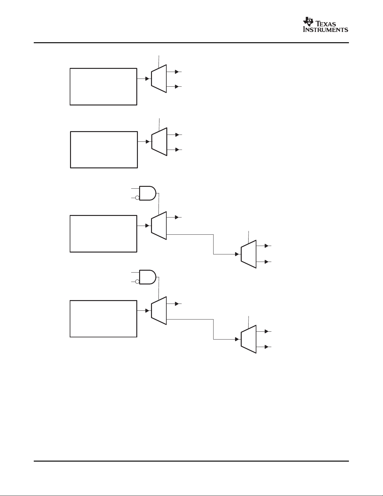
www.ti.com
1
0
VP0
Lower Data (10 pins)
VP0 (Channel A)
McBSP0
McBSP0EN [PERCFG.1]
1
0
VP1
Lower Data (10 pins)
VP1 (Channel A)
McBSP1
McBSP1EN [PERCFG.2]
1
0
VP0
Upper Data (10 pins)
VP0 (Channel B)
VP0 (Channel A)
McBSP0EN [PERCFG.1]
1
0
McASP0EN [PERCFG.0]
McASP0 Control
1
0
VP1
Upper Data (10 pins)
VP1 (Channel B)
VP1 (Channel A)
1
0
McASP0EN [PERCFG.0]
McASP0 Data
McASP0EN [PERCFG.0]
McBSP1EN [PERCFG.2]
McASP0EN [PERCFG.0]
VP0D[8:2] Muxed
(A)
VP0D[9,1,0] Standalone
VP1D[8:2] Muxed
(B)
VP1D[9,1,0] Standalone
VP0D[19:12] Muxed
(C)
VP0D[11:10] Standalone
VP1D[19:12] Muxed
(D)
VP1D[11:10] Standalone
TMS320DM642
Video/Imaging Fixed-Point Digital Signal Processor
SPRS200L – JULY 2002 – REVISED JANUARY 2007
A. Consists of: VP0D[8]/CLKR0, VP0D[7]/FSR0, VP0D[6]/DR0, VP0D[5]/CLKS0, VP0D[4]/DX0, VP0D[3]/FSX0,
B. Consists of: VP1D[8]/CLKR1, VP1D[7]/FSR1, VP1D[6]/DR1, VP1D[5]/CLKS1, VP1D[4]/DX1, VP1D[3]/FSX1,
C. Consists of: VP0D[19]/AHCLKX0, VP0D[18]/AFSX0, VP0D[17]/ACLKX0, VP0D[16]/AMUTE0, VP0D[15]/AMUTEIN0,
D. Consists of: VP1D[19:12]/AXR0[7:0]
VP0D[2]/CLKX0.
VP1D[2]/CLKX1.
VP0D[14]/AHCLKR0, VP0D[13]/AFSR0, VP0D[12]/ACLKR0
Figure 3-2. VP1, VP0, McBSP1, McBSP0, and McASP0 Data/Control Pin Muxing
58 Device Configurations Submit Documentation Feedback

www.ti.com
3.3 Peripheral Configuration Lock
Unlock the PERCFG Register
Using the PCFGLOCK Register
Write to
PERCFG Register
to Enable/Disable Peripherals
Read from
PERCFG Register
Wait 128 CPU Cycles Before
Accessing Enabled Peripherals
By default, the McASP0, VP0, VP1, VP2, and I2C peripherals are disabled on power up. In order to use
these peripherals on the DM642 device, the peripheral must first be enabled in the Peripheral
Configuration register (PERCFG). Software muxed pins should not be programmed to switch
functionalities during run-time. Care should also be taken to ensure that no accesses are being
performed before disabling the peripherals. To help minimize power consumption in the DM642
device, unused peripherals may be disabled.
Figure 3-3 shows the flow needed to enable (or disable) a given peripheral on the DM642 device.
TMS320DM642
Video/Imaging Fixed-Point Digital Signal Processor
SPRS200L – JULY 2002 – REVISED JANUARY 2007
Submit Documentation Feedback Device Configurations 59
Figure 3-3. Peripheral Enable/Disable Flow Diagram
www.ti.com
TMS320DM642
Video/Imaging Fixed-Point Digital Signal Processor
SPRS200L – JULY 2002 – REVISED JANUARY 2007
A 32-bit key (value = 0x10C0010C) must be written to the Peripheral Configuration Lock register
(PCFGLOCK) in order to unlock access to the PERCFG register. Reading the PCFGLOCK register
determines whether the PERCFG register is currently locked (LOCKSTAT bit = 1) or unlocked
(LOCKSTAT bit = 0), see Figure 3-4 . A peripheral can only be enabled when the PERCFG register is
"unlocked" (LOCKSTAT bit = 0).
Read Accesses
31 1 0
Reserved LOCKSTAT
R-0 R-1
Write Accesses
31 0
LOCK
W-0
Legend: R = Read only, R/W = Read/Write, - n = value after reset
Figure 3-4. PCFGLOCK Register Diagram [Address Location: 0x01B3 F018] - Read/Write Accesses
Table 3-5. PCFGLOCK Register Selection Bit Descriptions - Read Accesses
BIT NAME DESCRIPTION
31:1 Reserved Reserved. Read-only, writes have no effect.
Lock status bit.
Determines whether the PERCFG register is locked or unlocked.
0 LOCKSTAT 0 = Unlocked, read accesses to the PERCFG register allowed.
1 = Locked, write accesses to the PERCFG register do not modify the register state [default].
Reads are unaffected by Lock Status.
Table 3-6. PCFGLOCK Register Selection Bit Descriptions - Write Accesses
BIT NAME DESCRIPTION
31:0 LOCK
Lock bits.
0x10C0010C = Unlocks PERCFG register accesses.
Any write to the PERCFG register will automatically relock the register. In order to avoid the unnecessary
overhead of multiple unlock/enable sequences, all peripherals should be enabled with a single write to the
PERCFG register with the necessary enable bits set.
Prior to waiting 128 CPU cycles, the PERCFG register should be read. There is no direct correlation
between the CPU issuing a write to the PERCFG register and the write actually occurring. Reading the
PERCFG register after the write is issued forces the CPU to wait for the write to the PERCFG register to
occur.
Once a peripheral is enabled, the DSP (or other peripherals such as the HPI) must wait a minimum of 128
CPU cycles before accessing the enabled peripheral. The user must ensure that no accesses are
performed to a peripheral while it is disabled.
Device Configurations60 Submit Documentation Feedback
www.ti.com
Video/Imaging Fixed-Point Digital Signal Processor
SPRS200L – JULY 2002 – REVISED JANUARY 2007
3.4 Device Status Register Description
The device status register depicts the status of the device peripheral selection. For the actual register bit
names and their associated bit field descriptions, see Figure 3-5 and Table 3-7 .
31 24
Reserved
R-0
23 16
Reserved
R-0
15 12 11 10 9 8
Reserved MAC_EN HPI_WIDTH PCI_EEAI PCI_EN
R-0 R-x R-x R-x R-x
7 6 5 4 3 2 1 0
Reserved CLKMODE1 CLKMODE0 LENDIAN BOOTMODE1 BOOTMODE0 AECLKINSEL1 AECLKINSEL0
R-x R-x R-x R-x R-x R-x R-x R-x
Legend: R = Read only, R/W = Read/Write, - n = value after reset
Figure 3-5. Device Status Register (DEVSTAT) Description - 0x01B3 F004
TMS320DM642
Submit Documentation Feedback Device Configurations 61

www.ti.com
TMS320DM642
Video/Imaging Fixed-Point Digital Signal Processor
SPRS200L – JULY 2002 – REVISED JANUARY 2007
Table 3-7. Device Status (DEVSTAT) Register Selection Bit Descriptions
BIT NAME DESCRIPTION
31:12 Reserved Reserved. Read-only, writes have no effect.
EMAC enable bit.
Shows the status of whether EMAC peripheral is enabled or disabled (default).
11 MAC_EN 0 = EMAC is disabled, and the module is powered down (default).
10 HPI_WIDTH
9 PCI_EEAI
8 PCI_EN 0 = PCI disabled. (default).
7 Reserved Reserved. Read-only, writes have no effect.
6 CLKMODE1 Clock mode select bits
5 CLKMODE0
4 LENDIAN
3 BOOTMODE1 Bootmode configuration bits
2 BOOTMODE0
1 AECLKINSEL1 EMIFA input clock select
0 AECLKINSEL0
1 = EMAC is enabled.
This bit has no effect if the PCI peripheral is enabled (PCI_EN = 1).
HPI bus width control bit.
Shows the status of whether the HPI bus operates in 32-bit mode or in 16-bit mode (default).
0 = HPI operates in 16-bit mode. (default).
1 = HPI operates in 32-bit mode.
PCI EEPROM auto-initialization bit (PCI auto-initialization via external EEPROM).
Shows the status of whether the PCI module initializes internal registers via external EEPROM or if the
internal PCI default values are used instead (default).
0 = PCI auto-initialization through EEPROM is disabled; the PCI peripheral uses the specified PCI default
values (default).
1 = PCI auto-initialization through EEPROM is enabled; the PCI peripheral is configured through
EEPROM provided the PCI peripheral pin is enabled (PCI_EN = 1).
PCI enable bit.
Shows the status of whether the PCI peripheral is enabled or disabled (default).
1 = PCI enabled.
Global select for the PCI vs. HPI/EMAC/MDIO/GPIO peripherals.
Shows the status of whether the CPU clock frequency equals the input clock frequency X1 (Bypass), x6,
or x12.
Clock mode select for CPU clock frequency (CLKMODE[1:0])
00 - Bypass (x1) (default mode)
01 - x6
10 - x12
11 - Reserved
For more details on the CLKMODE pins and the PLL multiply factors, see the Clock PLL section of this
data sheet.
Device Endian mode (LEND)
Shows the status of whether the system is operating in Big Endian mode or Little Endian mode (default).
0 - System is operating in Big Endian mode
1 - System is operating in Little Endian mode (default)
Shows the status of what device bootmode configuration is operational.
Bootmode [1:0]
00 - No boot (default mode)
01 - HPI/PCI boot (based on PCI_EN pin)
10 - Reserved
11 - EMIFA boot
Shows the status of what clock mode is enabled or disabled for the EMIF.
Clock mode select for EMIFA (AECLKIN_SEL[1:0])
00 - AECLKIN (default mode)
01 - CPU/4 Clock Rate
10 - CPU/6 Clock Rate
11 - Reserved
Device Configurations62 Submit Documentation Feedback
www.ti.com
3.5 Multiplexed Pin Configurations
TMS320DM642
Video/Imaging Fixed-Point Digital Signal Processor
SPRS200L – JULY 2002 – REVISED JANUARY 2007
Multiplexed pins are pins that are shared by more than one peripheral and are internally multiplexed.
Some of these pins are configured by software, and the others are configured by external pullup/pulldown
resistors only at reset. Those muxed pins that are configured by software should not be programmed to
switch functionalities during run-time. Those muxed pins that are configured by external pullup/pulldown
resistors are mutually exclusive; only one peripheral has primary control of the function of these pins after
reset. Table 3-8 identifies the multiplexed pins on the DM642 device; shows the default (primary) function
and the default settings after reset; and describes the pins, registers, etc. necessary to configure specific
multiplexed functions.
Table 3-8. DM642 Device Multiplexed Pin Configurations
MULTIPLEXED PINS
NAME NO.
CLKOUT4/GP0[1] D6 CLKOUT4 GP1EN = 0 (disabled) These pins are software-configurable. To use these pins
CLKOUT6/GP0[2] C6 CLKOUT6 GP2EN = 0 (disabled)
VDAC/GP0[8] AD1 VDAC
GP0[9]/PIDSEL K3
GP0[10]/ PCBE3 J2
GP0[11]/ PREQ F1
GP0[12]/ PGNT H4 None
GP0[13]/ PINTA G4
GP0[14]/PCLK C1
GP0[15]/ PRST G3
VP1D[19]/AXR0[7] AB12
VP1D[18]/AXR0[6] AB11 By default, no function is enabled upon reset.
VP1D[17]/AXR0[5] AC11
VP1D[16]/AXR0[4] AD11
VP1D[15]/AXR0[3] AE11
VP1D[14]/AXR0[2] AC10
VP1D[13]/AXR0[1] AD10 data pins are disabled).
VP1D[12]/AXR0[0] AC9
(1) All other standalone PCI pins are tied-off internally (pins in Hi-Z) when the peripheral is disabled [PCI_EN = 0].
DEFAULT DEFAULT
FUNCTION SETTING
GP8EN = 0 (disabled)
MAC_EN = 0 (disabled)
GPxEN = 0 (disabled)
PCI_EN = 0 (disabled)
VP1EN bit = 0 (disabled) PERCFG register must be set to a 1. (McASP0 data pins
None MCASP0EN bit = 0 are disabled).
(disabled)
as GPIO pins, the GPxEN bits in the GPIO Enable
Register and the GPxDIR bits in the GPIO Direction
Register must be properly configured.
GPxEN = 1: GPx pin enabled
GPxDIR = 0: GPx pin is an input
GPxDIR = 1: GPx pin is an output
The VDAC output pin function is default.
To use GP0[8] as a GPIO pin, the PCI needs to be
disabled (PCI_EN = 0), the GPxEN bits in the GPIO
Enable Register and the GPxDIR bits in the GPIO
Direction Register must be properly configured.
GP8EN = 1: GP8 pin enabled
GP8DIR = 0: GP8 pin is an input
GP8DIR = 1: GP8 pin is an output
Note: If the PCI peripheral is disabled (PCI_EN pin = 0),
this pin must not be pulled up.
To use GP0[15:9] as GPIO pins, the PCI needs to be
disabled (PCI_EN = 0), the GPxEN bits in the GPIO
Enable Register and the GPxDIR bits in the GPIO
Direction Register must be properly configured.
(1)
GPxEN = 1: GPx pin enabled
GPxDIR = 0: GPx pin is an input
GPxDIR = 1: GPx pin is an output
To enable the Video Port 1 data pins, the VP1EN bit in the
To enable the McASP0[7:0] data pins, the MCASP0EN bit
in the PERCFG register must be set to a 1. (VP1 upper
(1)
DESCRIPTION
Submit Documentation Feedback Device Configurations 63

www.ti.com
TMS320DM642
Video/Imaging Fixed-Point Digital Signal Processor
SPRS200L – JULY 2002 – REVISED JANUARY 2007
Table 3-8. DM642 Device Multiplexed Pin Configurations
MULTIPLEXED PINS
NAME NO.
VP1D[8]/CLKR1 AD8
VP1D[7]/FSR1 AC7
VP1D[6]/DR1 AD7
VP1D[5]/CLKS1 AE7 MCBSP1EN bit = 1
VP1D[4]/DX1 AC6
VP1D[3]/FSX1 AD6
VP1D[2]/CLKX1 AE6
VP0D[19]/AHCLKX0 AC12
VP0D[18]/AFSX0 AD12 By default, no function is enabled upon reset.
VP0D[17]/ACLKX0 AB13
VP0D[16]/AMUTE0 AC13
VP0D[15]/AMUTEIN0 AD13
VP0D[14]/AHCLKR0 AB14
VP0D[13]/AFSR0 AC14 pins are disabled).
VP0D[12]/ACLKR0 AD14
VP0D[8]/CLKR0 AE15
VP0D[7]/FSR0 AB16
VP0D[6]/DR0 AC16
VP0D[5]/CLKS0 AD16 MCBSP0EN bit = 1
VP0D[4]/DX0 AE16
VP0D[3]/FSX0 AF16
VP0D[2]/CLKX0 AF17
XSP_CLK/MDCLK R5 By default, no functions enabled upon reset (PCI is
XSP_DO/MDIO P5
HAS/PPAR P3 HAS
HCNTL1/ PDEVSEL P1 HCNTL1
HCNTL0/ PSTOP R3 HCNTL0
HDS1/ PSERR R2 HDS1
HDS2/ PCBE1 T2 HDS2
HR/ W/ PCBE2 M1 HR/ W
HHWIL/ PTRDY N3
HINT/ PFRAME N4 HINT
HCS/ PPERR R1 HCS
HRDY/ PIRDY N1 HRDY
DEFAULT DEFAULT
FUNCTION SETTING
McBSP1
functions
None MCASP0EN bit = 0 pins are disabled).
McBSP0
functions
None MAC_EN = 0 PCI_EN = 1 at reset)
HHWIL
(HPI16 only)
VP1EN bit = 0 (disabled)
(enabled)
VP0EN bit = 0 (disabled) PERCFG register must be set to a 1. (McASP0 control
(disabled)
VP0EN bit = 0 (disabled)
(enabled)
PCI_EN = 0 (disabled)
(disabled)
PCI_EN = 0 (disabled)
(1)
By default, the McBSP1 peripheral, function is enabled
upon reset (MCBSP1EN bit = 1).
To enable the Video Port 1 data pins, the VP1EN bit in the
PERCFG register must be set to a 1.
To enable the Video Port 0 data pins, the VP0EN bit in the
To enable the McASP0 control pins, the MCASP0EN bit in
the PERCFG register must be set to a 1. (VP0 upper data
By default, the McBSP0 peripheral function is enabled
upon reset (MCBSP0EN bit = 1).
To enable the Video Port 0 data pins, the VP0EN bit in the
PERCFG register must be set to a 1.
disabled).
To enable the PCI peripheral, an external pullup resistor
(1)
(1 k Ω ) must be provided on the PCI_EN pin (setting
To enable the MDIO peripheral (which also enables the
EMAC peripheral), an external pullup resistor (1 k Ω ) must
be provided on the MAC_EN pin (setting MAC_EN = 1 at
reset)
By default, HPI is enabled upon reset (PCI is disabled).
(1)
To enable the PCI peripheral, an external pullup resistor
(1 k Ω ) must be provided on the PCI_EN pin (setting
PCI_EN = 1 at reset).
(1)
(continued)
DESCRIPTION
Device Configurations64 Submit Documentation Feedback

www.ti.com
Video/Imaging Fixed-Point Digital Signal Processor
Table 3-8. DM642 Device Multiplexed Pin Configurations
MULTIPLEXED PINS
NAME NO.
HD[23,15:0]/AD[23,15:0]
HD31/AD31/MRCLK G1 HD31
HD30/AD30/MCRS H3 HD30
HD29/AD29/MRXER G2 HD29
HD28/AD28/MRXDV J4 HD28
HD27/AD27/MRXD3 H2 HD27
HD26/AD26/MRXD2 J3 HD26
HD25/AD25/MRXD1 J1 HD25
HD24/AD24/MRXD0 K4 HD24 MAC_EN = 0 PCI_EN = 1 at reset).
HD22/AD22/MTCLK L4 HD22
HD21/AD21/MCOL K2 HD21
HD20/AD20/MTXEN L3 HD20
HD19/AD19/MTXD3 L2 HD19
HD18/AD18/MTXD2 M4 HD18
HD17/AD17/MTXD1 M2 HD17
HD16/AD16/MTXD0 M3 HD16
(2)
DEFAULT DEFAULT
FUNCTION SETTING
HD[23, 15:0] PCI_EN = 0 (disabled)
PCI_EN = 0 (disabled)
(disabled)
By default, HPI is enabled upon reset (PCI is disabled).
(1)
To enable the PCI peripheral, an external pullup resistor
(1 k Ω ) must be provided on the PCI_EN pin (setting
PCI_EN = 1 at reset).
By default, HPI is enabled upon reset (PCI is disabled).
To enable the PCI peripheral, an external pullup resistor
(1)
(1 k Ω ) must be provided on the PCI_EN pin (setting
(1)
To enable the EMAC peripheral, an external pullup resistor
(1 k Ω ) must be provided on the MAC_EN pin (setting
MAC_EN = 1 at reset).
TMS320DM642
SPRS200L – JULY 2002 – REVISED JANUARY 2007
(1)
(continued)
DESCRIPTION
3.6 Debugging Considerations
It is recommended that external connections be provided to device configuration pins, including
TOUT1/LENDIAN, AEA[22:19], GP0[3]/PCIEEAI, VDAC/GP0[8]/ PCI66, HD5/AD5, PCI_EN, and
TOUT0/MAC_EN. Although internal pullup/pulldown resistors exist on these pins, providing external
connectivity adds convenience to the user in debugging and flexibility in switching operating modes.
Internal pullup/pulldown resistors also exist on the non-configuration pins on the AEA bus (AEA[18:0]). Do
not oppose the internal pullup/pulldown resistors on these non-configuration pins with external
pullup/pulldown resistors. If an external controller provides signals to these non-configuration pins, these
signals must be driven to the default state of the pins at reset, or not be driven at all.
For the internal pullup/pulldown resistors for all device pins, see the terminal functions table.
Submit Documentation Feedback Device Configurations 65

www.ti.com
TMS320DM642
Video/Imaging Fixed-Point Digital Signal Processor
SPRS200L – JULY 2002 – REVISED JANUARY 2007
3.7 Configuration Examples
Figure 3-6 through Figure 3-8 illustrate examples of peripheral selections that are configurable on the
DM642 device.
Device Configurations66 Submit Documentation Feedback

www.ti.com
PERCFG Register Value: 0x0000 0078
External Pins: PCI_EN = 0 GP0[3]/PCIEEAI = 0 HD5 = 0 TOUT0/MAC_EN = 1
PCI
HPI
(16-Bit)
EMAC
MDIO
VP0
(20-Bit)
McBSP0
McASP0 Data
McBSP1
EMIFA
Clock
and
System
GP0
and
EXT_INT
I2C0
VP2
(20-Bit)
VIC
TIMER0
TIMER1
TIMER2
McASP0 Control
16
HD[15:0]
MTXD[3:0], MTXEN
MRXD[3:0], MRXER,
MRXDV, MCOL, MCRS,
MTCLK, MRCLK
MDIO, MDCLK
VP0CLK0
VP0CLK1,
VP0CTL[2:0],
VP0D[19:0]
VP1
(20-Bit)
VP1CLK0
VP1CLK1,
VP1CTL[2:0],
VP1D[19:0]
AED[63:0]
64
AECLKIN, AARDY, AHOLD
AEA[22:3], ACE[3:0], ABE[7:0],
AECLKOUT1, AECLKOUT2,
ASDCKE, ASOE3, APDT,
AHOLDA, ABUSREQ,
AARE/ASDCAS/ASADS/ASRE,
AAOE/ASDRAS/ASOE,
AAWE/ASDWE/ASWE
CLKIN,
CLKMODE0, CLKMODE1
CLKOUT4, CLKOUT6, PLLV
SCL0
SDA0
VP2CLK0
VP2CLK1,
VP2CTL[2:0],
VP2D[19:0]
TINP0
TOUT0/MACEN
TINP1
TOUT1/LENDIAN
STCLK
(A)
VDAC/GP0[8]/PCI66
HRDY, HINT
HCNTL0, HCNTL1,
HHWIL, HAS, HR/W,
HCS, HDS1, HDS2
GP0[15:9, 3:0]
GP0[7:4]
STCLK
(A)
STCLK
(A)
Shading denotes a peripheral module not available for this configuration.
A. STCLK supports all three video ports (VP2, VP1, and VP0).
TMS320DM642
Video/Imaging Fixed-Point Digital Signal Processor
SPRS200L – JULY 2002 – REVISED JANUARY 2007
Figure 3-6. Configuration Example A
(3 20-Bit Video Ports + HPI + EMAC + MDIO + I2C0 + EMIF + 3 Timers)
Submit Documentation Feedback Device Configurations 67

www.ti.com
McASP0 Data
McASP0 Control
PERCFG Register Value: 0x0000 007E
Extenal Pins: PCI_EN = 0 GP0[3]/PCIEEAI = 0 HD5 = 0 TOUT0/MAC_EN = 1
PCI
HPI
(16-Bit)
EMAC
MDIO
VP0
(10-Bit)
McBSP0
McBSP1
EMIFA
Clock
and
System
GP0
and
EXT_INT
I2C0
VP2
(20-Bit)
VIC
TIMER0
TIMER1
TIMER2
16
HD[15:0]
MTXD[3:0], MTXEN
MRXD[3:0], MRXER,
MRXDV, MCOL, MCRS,
MTCLK, MRCLK
MDIO, MDCLK
VP0CLK0
VP0CLK1,
VP0CTL[2:0],
VP0D[19:10]
VP1
(10-Bit)
VP1CLK0
VP1CLK1,
VP1CTL[2:0],
VP1D[19:10]
AED[63:0]
64
AECLKIN, AARDY, AHOLD
AEA[22:3], ACE[3:0], ABE[7:0],
AECLKOUT1, AECLKOUT2,
ASDCKE, ASOE3, APDT,
AHOLDA, ABUSREQ,
AARE/ASDCAS/ASADS/ASRE,
AAOE/ASDRAS/ASOE,
AAWE/ASDWE/ASWE
CLKIN,
CLKMODE0, CLKMODE1
CLKOUT4, CLKOUT6, PLLV
SCL0
SDA0
VP2CLK0
VP2CLK1,
VP2CTL[2:0],
VP2D[19:0]
TINP0
TOUT0/MACEN
TINP1
TOUT1/LENDIAN
STCLK
(A)
VDAC/GP0[8]/PCI66
HRDY, HINT
HCNTL0, HCNTL1,
HHWIL, HAS, HR/W,
HCS, HDS1, HDS2
GP0[15:9, 3:0]
GP0[7:4]
STCLK
(A)
STCLK
(A)
CLKR0, FSR0, DR0,
CLKS0, DX0, FSX0,
CLKX0
CLKR1, FSR1, DR1,
CLKS1, DX1, FSX1,
CLKX1
Shading denotes a peripheral module not available for this configuration.
A. STCLK supports all three video ports (VP2, VP1, and VP0).
TMS320DM642
Video/Imaging Fixed-Point Digital Signal Processor
SPRS200L – JULY 2002 – REVISED JANUARY 2007
(2 10-Bit Video Ports + 2 McBSPs + EMAC + MDIO + I2C0 + EMIF)
Figure 3-7. Configuration Example B
[Possible Video IP Phone Application]
Device Configurations68 Submit Documentation Feedback

www.ti.com
Shading denotes a peripheral module not available for this configuration.
PCI
HPI
(16-Bit)
EMAC
MDIO
VP0
(10-Bit)
McBSP0
McASP0 Data
McBSP1
EMIFA
Clock
and
System
GP0
and
EXT_INT
I2C0
VP2
(20-Bit)
VIC
TIMER0
TIMER1
TIMER2
McASP0 Control
16
HD[15:0]
MTXD[3:0], MTXEN
MRXD[3:0], MRXER,
MRXDV, MCOL, MCRS,
MTCLK, MRCLK
MDIO, MDCLK
VP0CLK0
VP0CLK1,
VP0CTL[2:0],
VP0D[9:0]
VP1
(10-Bit)
VP1CLK0
VP1CLK1,
VP1CTL[2:0],
VP1D[9:0]
AED[63:0]
64
AECLKIN, AARDY, AHOLD
AEA[22:3], ACE[3:0], ABE[7:0],
AECLKOUT1, AECLKOUT2,
ASDCKE, ASOE3, APDT,
AHOLDA, ABUSREQ,
AARE/ASDCAS/ASADS/ASRE,
AAOE/ASDRAS/ASOE,
AAWE/ASDWE/ASWE
CLKIN,
CLKMODE0, CLKMODE1
CLKOUT4, CLKOUT6, PLLV
SCL0
SDA0
VP2CLK0
VP2CLK1,
VP2CTL[2:0],
VP2D[19:0]
TINP0
TOUT0/MACEN
TINP1
TOUT1/LENDIAN
STCLK
(A)
VDAC/GP0[8]/PCI66
HRDY, HINT
HCNTL0, HCNTL1,
HHWIL, HAS, HR/W,
HCS, HDS1, HDS2
GP0[15:9, 3:0]
GP0[7:4]
STCLK
(A)
STCLK
(A)
AHCLKX0, AFSX0,
ACLKX0, AMUTE0,
AMUTEIN0, AHCLKR0,
AFSR0, ACLKR0
AXR0[7:0]
PERCFG Register Value: 0x0000 0079
Extenal Pins: PCI_EN = 0 GP0[3]/PCIEEAI = 0 HD5 = 0 TOUT0/MAC_EN = 1
A. STCLK supports all three video ports (VP2, VP1, and VP0).
TMS320DM642
Video/Imaging Fixed-Point Digital Signal Processor
SPRS200L – JULY 2002 – REVISED JANUARY 2007
(1 20-Bit Video Port, 2 10-Bit Video Ports + 1 McASP0 + VIC + I2C0 + EMIF)
Figure 3-8. Configuration Example C
[Possible Set-Top Box Application]
Submit Documentation Feedback Device Configurations 69

www.ti.com
TMS320DM642
Video/Imaging Fixed-Point Digital Signal Processor
SPRS200L – JULY 2002 – REVISED JANUARY 2007
4 Device Operating Conditions
4.1 Absolute Maximum Ratings Over Operating Case Temperature Range (Unless Otherwise Noted)
Supply voltage ranges:
Input voltage ranges:
Output voltage ranges:
Operating case temperature ranges, TC:
Storage temperature range, T
Package Temperature Cycling:
: –65°C to 150°C
stg
(1)
(2)
CV
DD
(2)
DV
DD
(except PCI), V
(PCI), V
(except PCI), V
(PCI), V
I
IP
O
OP
–0.5 V to DV
–0.5 V to DV
(default) 0°C to 90°C
(A version) [A-500, A-600] –40°C to 105°C
Temperature Range –40°C to 125°C
Number of Cycles 500
(1) Stresses beyond those listed under "absolute maximum ratings" may cause permanent damage to the device. These are stress ratings
only, and functional operation of the device at these or any other conditions beyond those indicated under "recommended operating
conditions" is not implied. Exposure to absolute-maximum-rated conditions for extended periods may affect device reliability.
(2) All voltage values are with respect to V
SS.
4.2 Recommended Operating Conditions
MIN NOM MAX UNIT
CV
DV
V
V
V
V
V
V
V
T
Supply voltage, Core (–500 device)
DD
Supply voltage, Core (A-500, A-600, -600, -720 devices)
Supply voltage, I/O 3.14 3.3 3.46 V
DD
Supply ground 0 0 0 V
SS
High-level input voltage (except PCI) 2 V
IH
Low-level input voltage (except PCI) 0.8 V
IL
Input voltage (PCI) –0.5 DV
IP
High-level input voltage (PCI) 0.5DV
IHP
Low-level input voltage (PCI) –0.5 0.3DV
ILP
Maximum voltage during overshoot/undershoot –1.0
OS
Operating case temperature
C
(1) Future variants of the C64x DSPs may operate at voltages ranging from 0.9 V to 1.4 V to provide a range of system power/performance
options. TI highly recommends that users design-in a supply that can handle multiple voltages within this range (i.e., 1.2 V, 1.25 V,
1.3 V, 1.35 V, 1.4 V with ± 3% tolerances) by implementing simple board changes such as reference resistor values or input pin
configuration modifications. Examples of such supplies include the PT4660, PT5500, PT5520, PT6440, and PT6930 series from Power
Trends, a subsidiary of Texas Instruments. Not incorporating a flexible supply may limit the system's ability to easily adapt to future
versions of C64x devices.
(2) The absolute maximum ratings should not be exceeded for more than 30% of the cycle period.
(1)
(1)
1.14 1.2 1.26 V
1.36 1.4 1.44 V
DD
DD
(2)
DV
DD
Default 0 90 °C
A version (A-500 and A-600) –40 105 °C
–0.3 V to 1.8 V
–0.3 V to 4 V
–0.3 V to 4 V
+ 0.5 V
DD
–0.3 V to 4 V
+ 0.5 V
DD
+ 0.5 V
+ 0.5 V
DD
(2)
4.3
V
V
Device Operating Conditions70 Submit Documentation Feedback

www.ti.com
Video/Imaging Fixed-Point Digital Signal Processor
SPRS200L – JULY 2002 – REVISED JANUARY 2007
4.3 Electrical Characteristics Over Recommended Ranges of Supply Voltage and Operating Case Temperature (Unless Otherwise Noted)
PARAMETER TEST CONDITIONS
V
V
V
V
I
I
High-level output voltage (except PCI) DV
OH
High-level output voltage (PCI) I
OHP
Low-level output voltage (except PCI) DV
OL
Low-level output voltage (PCI) I
OLP
Input current (except PCI) 50 100 150 uA
I
IP
Input leakage current (PCI)
(4)
= MIN, IOH= MAX 2.4 V
DD
= –0.5 mA, DV
OHP
= MIN, IOL= MAX 0.4 V
DD
= 1.5 mA, DV
OLP
VI= V
resistor
VI= V
resistor
VI= V
pulldown resistor
to DV
SS
to DV
SS
(3)
to DV
SS
0 < VIP< DV
DD
= 3.3 V 0.1DV
DD
no opposing internal
DD
opposing internal pullup
DD
opposing internal
DD
(3)
= 3.3 V ±10 uA
DD
EMIF, CLKOUT4, CLKOUT6, EMUx –16 mA
I
High-level output current –8 mA
OH
Video Ports, Timer, TDO, GPIO
(Excluding GP0[15:9, 2, 1]), McBSP
PCI/HPI –0.5
EMIF, CLKOUT4, CLKOUT6, EMUx 16 mA
Video Ports, Timer, TDO, GPIO
I
OL
Low-level output current
(Excluding GP0[15:9, 2, 1]), McBSP
SCL0 and SDA0 3 mA
PCI/HPI 1.5
I
I
I
C
C
Off-state output current VO= DV
OZ
CV
Core supply current
CDD
I/O supply current
DDD
Input capacitance 10 pF
i
Output capacitance 10 pF
o
(5)
(5)
DD
CV
DD
CV
DD
DV
DD
DV
DD
DV
DD
or 0 V ±10 uA
DD
= 1.4 V, CPU clock = 720 MHz 1090 mA
= 1.4 V, CPU clock = 600 MHz 890 mA
= 1.2 V, CPU clock = 500 MHz 620 mA
= 3.3 V, CPU clock = 720 MHz 210 mA
= 3.3 V, CPU clock = 600 MHz 210 mA
= 3.3 V, CPU clock = 500 MHz 165 mA
(1)
= 3.3 V 0.9DV
MIN TYP MAX UNIT
DD
–150 –100 –50 uA
TMS320DM642
(2)
DD
±10 uA
V
(2)
V
(2)
mA
8 mA
(2)
mA
(1) For test conditions shown as MIN, MAX, or NOM, use the appropriate value specified in the recommended operating conditions table.
(2) These rated numbers are from the PCI specification version 2.3. The DC specification and AC specification are defined in Table 5-3 and
Table 5-4 , respectively.
(3) Applies only to pins with an internal pullup (IPU) or pulldown (IPD) resistor.
(4) PCI input leakage currents include Hi-Z output leakage for all bidirectional buffers with 3-state outputs.
(5) Measured with average activity (50% high/50% low power) at 25°C case temperature and 133-MHz EMIF for –600 and –720 speeds
(100-MHz EMIF for –500 speed). This model represents a device performing high-DSP-activity operations 50% of the time, and the
remainder performing low-DSP-activity operations. The high/low-DSP-activity models are defined as follows:
• High-DSP-Activity Model:
– CPU: 8 instructions/cycle with 2 LDDW instructions [L1 Data Memory: 128 bits/cycle via LDDW instructions;
L1 Program Memory: 256 bits/cycle; L2/EMIF EDMA: 50% writes, 50% reads to/from SDRAM (50% bit-switching)]
– McBSP: 2 channels at E1 rate
– Timers: 2 timers at maximum rate
• Low-DSP-Activity Model:
– CPU: 2 instructions/cycle with 1 LDH instruction [L1 Data Memory: 16 bits/cycle; L1 Program Memory: 256 bits per 4 cycles;
L2/EMIF EDMA: None]
– McBSP: 2 channels at E1 rate
– Timers: 2 timers at maximum rate
The actual current draw is highly application-dependent. For more details on core and I/O activity, refer to the TMS320DMx Power
Consumption Summary application report (literature number SPRA962).
Submit Documentation Feedback Device Operating Conditions 71

www.ti.com
TMS320DM642
Video/Imaging Fixed-Point Digital Signal Processor
SPRS200L – JULY 2002 – REVISED JANUARY 2007
Device Operating Conditions72 Submit Documentation Feedback

www.ti.com
5 DM642 Peripheral Information and Electrical Specifications
Transmission Line
4.0 pF 1.85 pF
Z0 = 50 Ω
(see note)
Tester Pin Electronics
Data Sheet Timing Reference Point
Output
Under
Test
NOTE: The data sheet provides timing at the device pin. For output timing analysis, the tester pin electronics and its transmission line ef fects must
be taken into account. A transmission line with a delay of 2 ns or longer can be used to produce the desired transmission line effect. The
transmission line is intended as a load only. It is not necessary to add or subtract the transmission line delay (2 ns or longer) from the data
sheet timings.
42 Ω 3.5 nH
Device Pin
(see note)
Input requirements in this data sheet are tested with an input slew rate of < 4 Volts per nanosecond (4 V/ns) at the device pin.
V
ref
= 1.5 V
V
ref
= VIL MAX (or VOL MAX or
V
ref
= VIH MIN (or VOH MIN or
V
IHP
MIN or V
OHP
MIN)
V
ILP
MAX or V
OLP
MAX)
5.1 Parameter Information
5.1.1 Parameter Information Device-Specific Information
TMS320DM642
Video/Imaging Fixed-Point Digital Signal Processor
SPRS200L – JULY 2002 – REVISED JANUARY 2007
The load capacitance value stated is only for characterization and measurement of AC timing signals. This
load capacitance value does not indicate the maximum load the device is capable of driving.
5.1.1.1 Signal Transition Levels
All input and output timing parameters are referenced to 1.5 V for both "0" and "1" logic levels.
Figure 5-2. Input and Output Voltage Reference Levels for AC Timing Measurements
All rise and fall transition timing parameters are referenced to V
V
MAX and V
OL
V
MIN for PCI output clocks.
OHP
5.1.1.2 Signal Transition Rates
All timings are tested with an input edge rate of 4 Volts per nanosecond (4 V/ns).
Figure 5-1. Test Load Circuit for AC Timing Measurements
MAX and V
MIN for output clocks, V
OH
Figure 5-3. Rise and Fall Transition Time Voltage Reference Levels
MAX and V
ILP
IHP
IL
MIN for PCI input clocks, and V
MIN for input clocks,
IH
MAX and
OLP
Submit Documentation Feedback DM642 Peripheral Information and Electrical Specifications 73
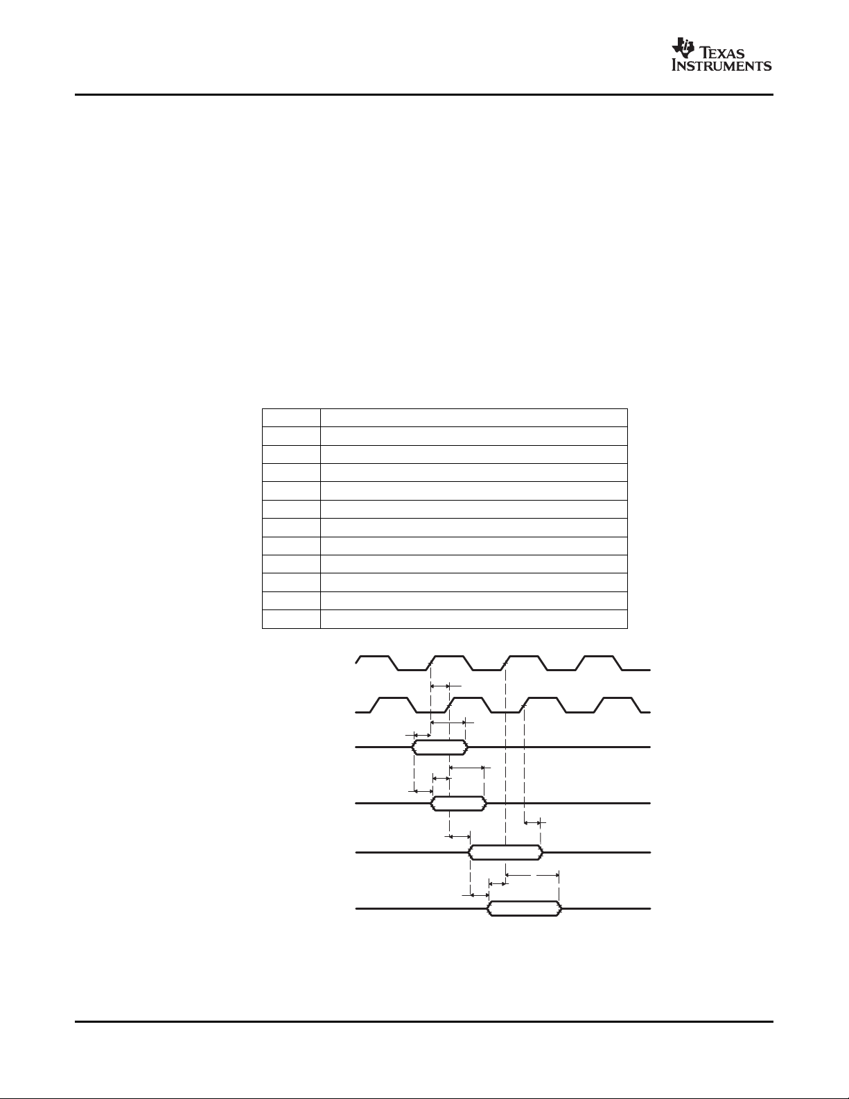
www.ti.com
1
2
3
4
5
6
7
8
10
11
ECLKOUTx
(Output from DSP)
ECLKOUTx
(Input to External Device)
Control Signals
(A)
(Output from DSP)
Control Signals
(Input to External Device)
Data Signals
(B)
(Output from External Device)
Data Signals
(B)
(Input to DSP)
9
TMS320DM642
Video/Imaging Fixed-Point Digital Signal Processor
SPRS200L – JULY 2002 – REVISED JANUARY 2007
5.1.1.3 Timing Parameters and Board Routing Analysis
The timing parameter values specified in this data sheet do not include delays by board routings. As a
good board design practice, such delays must always be taken into account. Timing values may be
adjusted by increasing/decreasing such delays. TI recommends utilizing the available I/O buffer
information specification (IBIS) models to analyze the timing characteristics correctly. To properly use IBIS
models to attain accurate timing analysis for a given system, see the Using IBIS Models for Timing
Analysis application report (literature number SPRA839). If needed, external logic hardware such as
buffers may be used to compensate any timing differences.
For inputs, timing is most impacted by the round-trip propagation delay from the DSP to the external
device and from the external device to the DSP. This round-trip delay tends to negatively impact the input
setup time margin, but also tends to improve the input hold time margins (see Table 5-1 and Figure 5-4 ).
Figure 5-4 represents a general transfer between the DSP and an external device. The figure also
represents board route delays and how they are perceived by the DSP and the external device.
Table 5-1. Board-Level Timing Example
NO. DESCRIPTION
1 Clock route delay
2 Minimum DSP hold time
3 Minimum DSP setup time
4 External device hold time requirement
5 External device setup time requirement
6 Control signal route delay
7 External device hold time
8 External device access time
9 DSP hold time requirement
10 DSP setup time requirement
11 Data route delay
(see Figure 5-4 )
A. Control signals include data for Writes.
B. Data signals are generated during Reads from an external device.
74 DM642 Peripheral Information and Electrical Specifications Submit Documentation Feedback
Figure 5-4. Board-Level Input/Output Timings
www.ti.com
5.2 Recommended Clock and Control Signal Transition Behavior
DV
DD
CV
DD
V
SS
C6000
DSP
Schottky
Diode
I/O Supply
Core Supply
GND
TMS320DM642
Video/Imaging Fixed-Point Digital Signal Processor
SPRS200L – JULY 2002 – REVISED JANUARY 2007
All clocks and control signals must transition between V
manner.
5.3 Power Supplies
For more information regarding TI's power management products and suggested devices to power TI
DSPs, visit www.ti.com/dsppower .
5.3.1 Power-Supply Sequencing
TI DSPs do not require specific power sequencing between the core supply and the I/O supply. However,
systems should be designed to ensure that neither supply is powered up for extended periods of time
(>1 second) if the other supply is below the proper operating voltage.
5.3.2 Power-Supply Design Considerations
A dual-power supply with simultaneous sequencing can be used to eliminate the delay between core and
I/O power up. A Schottky diode can also be used to tie the core rail to the I/O rail (see Figure 5-5 ).
and V
IH
(or between V
IL
and VIH) in a monotonic
IL
Figure 5-5. Schottky Diode Diagram
Core and I/O supply voltage regulators should be located close to the DSP (or DSP array) to minimize
inductance and resistance in the power delivery path. Additionally, when designing for high-performance
applications utilizing the C6000™ platform of DSPs, the PC board should include separate power planes
for core, I/O, and ground, all bypassed with high-quality low-ESL/ESR capacitors.
5.3.3 Power-Supply Decoupling
In order to properly decouple the supply planes from system noise, place as many capacitors (caps) as
possible close to the DSP. Assuming 0603 caps, the user should be able to fit a total of 60 caps, 30 for
the core supply and 30 for the I/O supply. These caps need to be close to the DSP power pins, no more
than 1.25 cm maximum distance to be effective. Physically smaller caps, such as 0402, are better
because of their lower parasitic inductance. Proper capacitance values are also important. Small bypass
caps (near 560 pF) should be closest to the power pins. Medium bypass caps (220 nF or as large as can
be obtained in a small package) should be next closest. TI recommends no less than 8 small and
8 medium caps per supply (32 total) be placed immediately next to the BGA vias, using the "interior" BGA
space and at least the corners of the "exterior".
Eight larger caps (4 for each supply) can be placed further away for bulk decoupling. Large bulk caps (on
the order of 100 µF) should be furthest away (but still as close as possible). No less than 4 large caps per
supply (8 total) should be placed outside of the BGA.
Submit Documentation Feedback DM642 Peripheral Information and Electrical Specifications 75

www.ti.com
PWRD
Internal Clock Tree
CPU
IFR
IER
CSR
PD1
PD2
Power-
Down
Logic
Clock
PLL
CLKIN RESET
CLKOUT6
PD3
Internal
Peripherals
CLKOUT4
Clock
and Dividers
Distribution
TMS320DM642
TMS320DM642
Video/Imaging Fixed-Point Digital Signal Processor
SPRS200L – JULY 2002 – REVISED JANUARY 2007
Any cap selection needs to be evaluated from a yield/manufacturing point-of-view. As with the selection of
any component, verification of capacitor availability over the product’s production lifetime should be
considered.
5.3.4 Peripheral Power-Down Operation
The DM642 device can be powered down in three ways:
• Power-down due to pin configuration
• Power-down due to software configuration – relates to the default state of the peripheral configuration
bits in the PERCFG register.
• Power-down during run-time via software configuration
On the DM642 device, the HPI, PCI, and EMAC and MDIO peripherals are controlled (selected) at the pin
level during chip reset (e.g., PCI_EN, HD5, and MAC_EN pins).
The McASP0, McBSP0, McBSP1, VP0, VP1, VP2, and I2C0 peripheral functions are selected via the
peripheral configuration (PERCFG) register bits.
For more detailed information on the peripheral configuration pins and the PERCFG register bits, see the
Device Configurations section of this document.
5.3.5 Power-Down Modes Logic
Figure 5-6 shows the power-down mode logic on the DM642.
A. External input clocks, with the exception of CLKIN, are not gated by the power-down mode logic.
Figure 5-6. Power-Down Mode Logic
(A)
76 DM642 Peripheral Information and Electrical Specifications Submit Documentation Feedback
www.ti.com
TMS320DM642
Video/Imaging Fixed-Point Digital Signal Processor
SPRS200L – JULY 2002 – REVISED JANUARY 2007
5.3.6 Triggering, Wake-up, and Effects
The power-down modes and their wake-up methods are programmed by setting the PWRD field (bits
15–10) of the control status register (CSR). The PWRD field of the CSR is shown in Figure 5-7 and
described in Table 5-2 . When writing to the CSR, all bits of the PWRD field should be set at the same
time. Logic 0 should be used when writing to the reserved bit (bit 15) of the PWRD field. The CSR is
discussed in detail in the TMS320C6000 CPU and Instruction Set Reference Guide (literature number
SPRU189).
31 16
(See NOTE)
15 14 13 12 11 10 9 8
Reserved Non-Enabled PD3 PD2 PD1 (See NOTE)
Enable or
Interrupt Wake
R/W-0 R/W-0 R/W-0 R/W-0 R/W-0 R/W-0
7 0
Legend: R/W = Readable/Writable, - n = value after reset
NOTE: The shaded bits are not part of the power-down logic discussion and therefore are not covered here. For information on these other
bit fields in the CSR register, see the TMS320C6000 CPU and Instruction Set Reference Guide (literature number SPRU189).
Enabled
Interrupt Wake
(See NOTE)
Figure 5-7. PWRD Field of the CSR Register
A delay of up to nine clock cycles may occur after the instruction that sets the PWRD bits in the CSR
before the PD mode takes effect. As best practice, NOPs should be padded after the PWRD bits are set in
the CSR to account for this delay.
If PD1 mode is terminated by a non-enabled interrupt, the program execution returns to the instruction
where PD1 took effect. If PD1 mode is terminated by an enabled interrupt, the interrupt service routine will
be executed first, then the program execution returns to the instruction where PD1 took effect. In the case
with an enabled interrupt, the GIE bit in the CSR and the NMIE bit in the interrupt enable register (IER)
must also be set in order for the interrupt service routine to execute; otherwise, execution returns to the
instruction where PD1 took effect upon PD1 mode termination by an enabled interrupt.
PD2 and PD3 modes can only be aborted by device reset. Table 5-2 summarizes all the power-down
modes.
Submit Documentation Feedback DM642 Peripheral Information and Electrical Specifications 77

www.ti.com
TMS320DM642
Video/Imaging Fixed-Point Digital Signal Processor
SPRS200L – JULY 2002 – REVISED JANUARY 2007
Table 5-2. Characteristics of the Power-Down Modes
PRWD Field POWER-DOWN
(BITS 15–10) MODE
000000 No power-down — —
001001 PD1 Wake by an enabled interrupt CPU halted (except for the interrupt logic)
010001 PD1
011010 PD2
011100 PD3
All others Reserved — —
(1) When entering PD2 and PD3, all functional I/O remains in the previous state. However, for peripherals which are asynchronous in
nature or peripherals with an external clock source, output signals may transition in response to stimulus on the inputs. Under these
conditions, peripherals will not operate according to specifications.
(1)
(1)
WAKE-UP METHOD EFFECT ON CHIP'S OPERATION
Power-down mode blocks the internal clock inputs at the
Wake by an enabled or
non-enabled interrupt
Wake by a device reset halted. All register and internal RAM contents are preserved. All
Wake by a device reset
boundary of the CPU, preventing most of the CPU's logic from
switching. During PD1, EDMA transactions can proceed
between peripherals and internal memory.
Output clock from PLL is halted, stopping the internal clock
structure from switching and resulting in the entire chip being
functional I/O "freeze" in the last state when the PLL clock is
turned off.
Input clock to the PLL stops generating clocks. All register and
internal RAM contents are preserved. All functional I/O "freeze"
in the last state when the PLL clock is turned off. Following
reset, the PLL needs time to re-lock, just as it does following
power-up.
Wake-up from PD3 takes longer than wake-up from PD2
because the PLL needs to be re-locked, just as it does following
power-up.
5.3.7 C64x Power-Down Mode with an Emulator
If user power-down modes are programmed, and an emulator is attached, the modes will be masked to
allow the emulator access to the system. This condition prevails until the emulator is reset or the cable is
removed from the header. If power measurements are to be performed when in a power-down mode, the
emulator cable should be removed.
When the DSP is in power-down mode PD2 or PD3, emulation logic will force any emulation execution
command (such as Step or Run) to spin in IDLE. For this reason, PC writes (such as loading code) will
fail. A DSP reset will be required to get the DSP out of PD2/PD3.
DM642 Peripheral Information and Electrical Specifications78 Submit Documentation Feedback
www.ti.com
5.4 Enhanced Direct Memory Access (EDMA) Controller
The EDMA controller handles all data transfers between the level-two (L2) cache/memory controller and
the device peripherals on the DM642 DSP. These data transfers include cache servicing, non-cacheable
memory accesses, user-programmed data transfers, and host accesses.
5.4.1 EDMA Device-Specific Information
5.4.1.1 EDMA Channel Synchronization Events
The C64x EDMA supports up to 64 EDMA channels which service peripheral devices and external
memory. Table 5-3 lists the source of C64x EDMA synchronization events associated with each of the
programmable EDMA channels. For the DM642 device, the association of an event to a channel is fixed;
each of the EDMA channels has one specific event associated with it. These specific events are captured
in the EDMA event registers (ERL, ERH) even if the events are disabled by the EDMA event enable
registers (EERL, EERH). The priority of each event can be specified independently in the transfer
parameters stored in the EDMA parameter RAM. For more detailed information on the EDMA module and
how EDMA events are enabled, captured, processed, linked, chained, and cleared, etc., see the
TMS320C6000 DSP Enhanced Direct Memory Access (EDMA) Controller Reference Guide (literature
number SPRU234).
TMS320DM642
Video/Imaging Fixed-Point Digital Signal Processor
SPRS200L – JULY 2002 – REVISED JANUARY 2007
Table 5-3. TMS320DM642 EDMA Channel Synchronization Events
EDMA
CHANNEL
0 DSP_INT HPI/PCI-to-DSP interrupt
1 TINT0 Timer 0 interrupt
2 TINT1 Timer 1 interrupt
3 SD_INTA EMIFA SDRAM timer interrupt
4 GPINT4/EXT_INT4 GP0 event 4/External interrupt pin 4
5 GPINT5/EXT_INT5 GP0 event 5/External interrupt pin 5
6 GPINT6/EXT_INT6 GP0 event 6/External interrupt pin 6
7 GPINT7/EXT_INT7 GP0 event 7/External interrupt pin 7
8 GPINT0 GP0 event 0
9 GPINT1 GP0 event 1
10 GPINT2 GP0 event 2
11 GPINT3 GP0 event 3
12 XEVT0 McBSP0 transmit event
13 REVT0 McBSP0 receive event
14 XEVT1 McBSP1 transmit event
15 REVT1 McBSP1 receive event
16 VP0EVTYA VP0 Channel A Y event DMA request
17 VP0EVTUA VP0 Channel A Cb event DMA request
18 VP0EVTVA VP0 Channel A Cr event DMA request
19 TINT2 Timer 2 interrupt
20–23 – None
24 VP0EVTYB VP0 Channel B Y event DMA request
25 VP0EVTUB VP0 Channel B Cb event DMA request
26 VP0EVTVB VP0 Channel B Cr event DMA request
27–31 – None
32 AXEVTE0 McASP0 transmit even event
EVENT NAME EVENT DESCRIPTION
(1)
(1) In addition to the events shown in this table, each of the 64 channels can also be synchronized with the transfer completion or alternate
transfer completion events. For more detailed information on EDMA event-transfer chaining, see the TMS320C6000 DSP Enhanced
Direct Memory Access (EDMA) Controller Reference Guide (literature number SPRU234).
Submit Documentation Feedback DM642 Peripheral Information and Electrical Specifications 79

www.ti.com
TMS320DM642
Video/Imaging Fixed-Point Digital Signal Processor
SPRS200L – JULY 2002 – REVISED JANUARY 2007
Table 5-3. TMS320DM642 EDMA Channel Synchronization Events (continued)
EDMA
CHANNEL
33 AXEVTO0 McASP0 transmit odd event
34 AXEVT0 McASP0 transmit event
35 AREVTE0 McASP0 receive even event
36 AREVTO0 McASP0 receive odd event
37 AREVT0 McASP0 receive event
38 VP1EVTYB VP1 Channel B Y event DMA request
39 VP1EVTUB VP1 Channel B Cb event DMA request
40 VP1EVTVB VP1 Channel B Cr event DMA request
41 VP2EVTYB VP2 Channel B Y event DMA request
42 VP2EVTUB VP2 Channel B Cb event DMA request
43 VP2EVTVB VP2 Channel B Cr event DMA request
44 ICREVT0 I2C0 receive event
45 ICXEVT0 I2C0 transmit event
46–47 – None
48 GPINT8 GP0 event 8
49 GPINT9 GP0 event 9
50 GPINT10 GP0 event 10
51 GPINT11 GP0 event 11
52 GPINT12 GP0 event 12
53 GPINT13 GP0 event 13
54 GPINT14 GP0 event 14
55 GPINT15 GP0 event 15
56 VP1EVTYA VP1 Channel A Y event DMA request
57 VP1EVTUA VP1 Channel A Cb event DMA request
58 VP1EVTVA VP1 Channel A Cr event DMA request
59 VP2EVTYA VP2 Channel A Y event DMA request
60 VP2EVTUA VP2 Channel A Cb event DMA request
61 VP2EVTVA VP2 Channel A Cr event DMA request
62–63 – None
EVENT NAME EVENT DESCRIPTION
DM642 Peripheral Information and Electrical Specifications80 Submit Documentation Feedback

www.ti.com
Video/Imaging Fixed-Point Digital Signal Processor
5.4.2 EDMA Peripheral Register Description(s)
Table 5-4. EDMA Registers (C64x)
HEX ADDRESS RANGE ACRONYM REGISTER NAME
01A0 0800 – 01A0 FF98 – Reserved
01A0 FF9C EPRH Event polarity high register
01A0 FFA4 CIPRH Channel interrupt pending high register
01A0 FFA8 CIERH Channel interrupt enable high register
01A0 FFAC CCERH Channel chain enable high register
01A0 FFB0 ERH Event high register
01A0 FFB4 EERH Event enable high register
01A0 FFB8 ECRH Event clear high register
01A0 FFBC ESRH Event set high register
01A0 FFC0 PQAR0 Priority queue allocation register 0
01A0 FFC4 PQAR1 Priority queue allocation register 1
01A0 FFC8 PQAR2 Priority queue allocation register 2
01A0 FFCC PQAR3 Priority queue allocation register 3
01A0 FFDC EPRL Event polarity low register
01A0 FFE0 PQSR Priority queue status register
01A0 FFE4 CIPRL Channel interrupt pending low register
01A0 FFE8 CIERL Channel interrupt enable low register
01A0 FFEC CCERL Channel chain enable low register
01A0 FFF0 ERL Event low register
01A0 FFF4 EERL Event enable low register
01A0 FFF8 ECRL Event clear low register
01A0 FFFC ESRL Event set low register
01A1 0000 – 01A3 FFFF – Reserved
TMS320DM642
SPRS200L – JULY 2002 – REVISED JANUARY 2007
Table 5-5. Quick DMA (QDMA) and Pseudo Registers
HEX ADDRESS RANGE ACRONYM REGISTER NAME
0200 0000 QOPT QDMA options parameter register
0200 0004 QSRC QDMA source address register
0200 0008 QCNT QDMA frame count register
0200 000C QDST QDMA destination address register
0200 0010 QIDX QDMA index register
0200 0014 – 0200 001C Reserved
0200 0020 QSOPT QDMA pseudo options register
0200 0024 QSSRC QDMA psuedo source address register
0200 0028 QSCNT QDMA psuedo frame count register
0200 002C QSDST QDMA destination address register
0200 0030 QSIDX QDMA psuedo index register
Submit Documentation Feedback DM642 Peripheral Information and Electrical Specifications 81

www.ti.com
TMS320DM642
Video/Imaging Fixed-Point Digital Signal Processor
SPRS200L – JULY 2002 – REVISED JANUARY 2007
Table 5-6. EDMA Parameter RAM (C64x)
HEX ADDRESS RANGE ACRONYM REGISTER NAME COMMENTS
01A0 0000 – 01A0 0017 – Parameters for Event 0 (6 words) (6 words) or Reload/Link
01A0 0018 – 01A0 002F – Parameters for Event 1 (6 words)
01A0 0030 – 01A0 0047 – Parameters for Event 2 (6 words)
01A0 0048 – 01A0 005F – Parameters for Event 3 (6 words)
01A0 0060 – 01A0 0077 – Parameters for Event 4 (6 words)
01A0 0078 – 01A0 008F – Parameters for Event 5 (6 words)
01A0 0090 – 01A0 00A7 – Parameters for Event 6 (6 words)
01A0 00A8 – 01A0 00BF – Parameters for Event 7 (6 words)
01A0 00C0 – 01A0 00D7 – Parameters for Event 8 (6 words)
01A0 00D8 – 01A0 00EF – Parameters for Event 9 (6 words)
01A0 00F0 – 01A0 00107 – Parameters for Event 10 (6 words)
01A0 0108 – 01A0 011F – Parameters for Event 11 (6 words)
01A0 0120 – 01A0 0137 – Parameters for Event 12 (6 words)
01A0 0138 – 01A0 014F – Parameters for Event 13 (6 words)
01A0 0150 – 01A0 0167 – Parameters for Event 14 (6 words)
01A0 0168 – 01A0 017F – Parameters for Event 15 (6 words)
01A0 0180 – 01A0 0197 – Parameters for Event 16 (6 words)
01A0 0198 – 01A0 01AF – Parameters for Event 17 (6 words)
... ...
01A0 05D0 – 01A0 05E7 – Parameters for Event 62 (6 words)
01A0 05E8 – 01A0 05FF – Parameters for Event 63 (6 words)
01A0 0600 – 01A0 0617 – Reload/link parameters for Event 0 (6 words)
01A0 0618 – 01A0 062F – Reload/link parameters for Event 1 (6 words)
... ...
01A0 07E0 – 01A0 07F7 – Reload/link parameters for Event 20 (6 words)
01A0 07F8 – 01A0 080F – Reload/link parameters for Event 21 (6 words)
01A0 0810 – 01A0 0827 – Reload/link parameters for Event 22 (6 words)
... ...
01A0 13C8 – 01A0 13DF – Reload/link parameters for Event 147 (6 words)
01A0 13E0 – 01A0 13F7 – Reload/link parameters for Event 148 (6 words)
01A0 13F8 – 01A0 13FF – Scratch pad area (2 words)
01A0 1400 – 01A3 FFFF – Reserved
(1) The DM642 device has 213 EDMA parameters total: 64-Event/Reload channels and 149-Reload only parameter sets [six (6) words
each] that can be used to reload/link EDMA transfers.
(1)
Parameters for Event 0
Parameters for other Event
Reload/Link Parameters for
other Event 0–15
82 DM642 Peripheral Information and Electrical Specifications Submit Documentation Feedback

www.ti.com
5.5 Interrupts
5.5.1 Interrupt Sources and Interrupt Selector
The C64x DSP core supports 16 prioritized interrupts, which are listed in Table 5-7 . The highest-priority
interrupt is INT_00 (dedicated to RESET) while the lowest-priority interrupt is INT_15. The first four
interrupts (INT_00–INT_03) are non-maskable and fixed. The remaining interrupts (INT_04–INT_15) are
maskable and default to the interrupt source specified in Table 5-7 . The interrupt source for interrupts
4–15 can be programmed by modifying the selector value (binary value) in the corresponding fields of the
Interrupt Selector Control registers: MUXH (address 0x019C0000) and MUXL (address 0x019C0004).
TMS320DM642
Video/Imaging Fixed-Point Digital Signal Processor
SPRS200L – JULY 2002 – REVISED JANUARY 2007
Table 5-7. DM642 DSP Interrupts
CPU SELECTOR
INTERRUPT VALUE INTERRUPT SOURCE
NUMBER (BINARY)
(1)
INT_00
(1)
INT_01
(1)
INT_02
(1)
INT_03
(2)
INT_04
(2)
INT_05
(2)
INT_06
(2)
INT_07
(2)
INT_08
(2)
INT_09
(2)
INT_10
(2)
INT_11
(2)
INT_12
(2)
INT_13
(2)
INT_14
(2)
INT_15
INTERRUPT
SELECTOR INTERRUPT
CONTROL EVENT
REGISTER
– – RESET
– – NMI
– – Reserved Reserved. Do not use.
– – Reserved Reserved. Do not use.
MUXL[4:0] 00100 GPINT4/EXT_INT4 GP0 interrupt 4/External interrupt pin 4
MUXL[9:5] 00101 GPINT5/EXT_INT5 GP0 interrupt 5/External interrupt pin 5
MUXL[14:10] 00110 GPINT6/EXT_INT6 GP0 interrupt 6/External interrupt pin 6
MUXL[20:16] 00111 GPINT7/EXT_INT7 GP0 interrupt 7/External interrupt pin 7
MUXL[25:21] 01000 EDMA_INT EDMA channel (0 through 63) interrupt
MUXL[30:26] 01001 EMU_DTDMA EMU DTDMA
MUXH[4:0] 00011 SD_INTA EMIFA SDRAM timer interrupt
MUXH[9:5] 01010 EMU_RTDXRX EMU real-time data exchange (RTDX) receive
MUXH[14:10] 01011 EMU_RTDXTX EMU RTDX transmit
MUXH[20:16] 00000 DSP_INT HPI/PCI-to-DSP interrupt
MUXH[25:21] 00001 TINT0 Timer 0 interrupt
MUXH[30:26] 00010 TINT1 Timer 1 interrupt
– – 01100 XINT0 McBSP0 transmit interrupt
– – 01101 RINT0 McBSP0 receive interrupt
– – 01110 XINT1 McBSP1 transmit interrupt
– – 01111 RINT1 McBSP1 receive interrupt
– – 10000 GPINT0 GP0 interrupt 0
– – 10001 Reserved Reserved. Do not use.
– – 10010 Reserved Reserved. Do not use.
– – 10011 TINT2 Timer 2 interrupt
– – 10100 Reserved Reserved. Do not use.
– – 10101 Reserved Reserved. Do not use.
– – 10110 ICINT0 I2C0 interrupt
– – 10111 Reserved Reserved. Do not use.
– – 11000 EMAC_MDIO_INT EMAC/MDIO interrupt
– – 11001 VPINT0 VP0 interrupt
– – 11010 VPINT1 VP1 interrupt
– – 11011 VPINT2 VP2 interrupt
(1) Interrupts INT_00 through INT_03 are non-maskable and fixed.Interrupts
(2) INT_04 through INT_15 are programmable by modifying the binary selector values in the Interrupt Selector Control registers fields.
Table 5-7 shows the default interrupt sources for Interrupts INT_04 through INT_15. For more detailed information on interrupt sources
and selection, see the TMS320C6000 DSP Interrupt Selector Reference Guide (literature number SPRU646).
Submit Documentation Feedback DM642 Peripheral Information and Electrical Specifications 83

www.ti.com
2
1
EXT_INTx, NMI
TMS320DM642
Video/Imaging Fixed-Point Digital Signal Processor
SPRS200L – JULY 2002 – REVISED JANUARY 2007
Table 5-7. DM642 DSP Interrupts (continued)
CPU SELECTOR
INTERRUPT VALUE INTERRUPT SOURCE
NUMBER (BINARY)
– – 11100 AXINT0 McASP0 transmit interrupt
– – 11101 ARINT0 McASP0 receive interrupt
– – 11110 – 11111 Reserved Reserved. Do not use.
5.5.2 Interrupts Peripheral Register Description(s)
HEX ADDRESS RANGE ACRONYM REGISTER NAME COMMENTS
019C 0000 MUXH Interrupt multiplexer high
019C 0004 MUXL Interrupt multiplexer low
019C 0008 EXTPOL External interrupt polarity
019C 000C – 019F FFFF – Reserved
INTERRUPT
SELECTOR INTERRUPT
CONTROL EVENT
REGISTER
Table 5-8. Interrupt Selector Registers (C64x)
Selects which interrupts drive CPU
interrupts 10–15 (INT10–INT15)
Selects which interrupts drive CPU
interrupts 4–9 (INT04–INT09)
Sets the polarity of the external
interrupts (EXT_INT4–EXT_INT7)
5.5.3 External Interrupts Electrical Data/Timing
Table 5-9. Timing Requirements for External Interrupts
NO. UNIT
1 t
w(ILOW)
2 t
w(IHIGH)
(1) P = 1/CPU clock frequency in ns. For example, when running parts at 720 MHz, use P = 1.39 ns.
Width of the NMI interrupt pulse low 4P ns
Width of the EXT_INT interrupt pulse low 8P ns
Width of the NMI interrupt pulse high 4P ns
Width of the EXT_INT interrupt pulse high 8P ns
Figure 5-8. External/NMI Interrupt Timing
(1)
(see Figure 5-8 )
–500
–600
–720
MIN MAX
84 DM642 Peripheral Information and Electrical Specifications Submit Documentation Feedback
www.ti.com
5.6 Reset
A hardware reset ( RESET) is required to place the DSP into a known good state out of power-up. The
RESET signal can be asserted (pulled low) prior to ramping the core and I/O voltages or after the core
and I/O voltages have reached their proper operating conditions. As a best practice, reset should be held
low during power-up. Prior to deasserting RESET (low-to-high transition), the core and I/O voltages should
be at their proper operating conditions and CLKIN should also be running at the correct frequency. When
PCI is enabled, the PCI input clock (PCLK) must be running prior to deasserting RESET as well.
When the PCI peripheral is enabled, a WARMRESET can be performed via the host. A WARMRESET
performs the same functionality as a hardware reset, but does not relatch the boot configuration pins.
Whatever boot configuration that was latched on the previous hardware reset will be performed during the
WARMRESET.
A hardware reset does not reset the PCI peripheral state machine. The PCI state machine is reset via the
PRST signal. The PRST signal does not affect the DSP.
Emulation resets, done using Code Composer Studio™ IDE, have the same affect as a PCI
WARMRESET.
For information on peripheral selection at the rising edge of RESET, see the Device Configuration section
of this data manual.
5.6.1 Reset Electrical Data/Timing
TMS320DM642
Video/Imaging Fixed-Point Digital Signal Processor
SPRS200L – JULY 2002 – REVISED JANUARY 2007
Table 5-10. Timing Requirements for Reset (see Figure 5-9 )
–500
NO. UNIT
1 t
w(RST)
16 t
su(boot)
17 t
h(boot)
18 t
su(PCLK-RSTH)
(1) AEA[22:19], LENDIAN, PCIEEAI, and HD5/AD5 are the boot configuration pins during device reset.
(2) E = 1/AECLKIN clock frequency in ns. C = 1/CLKIN clock frequency in ns.
Select the MIN parameter value, whichever value is larger.
(3) P = 1/CPU clock frequency in ns. For example, when running parts at 720 MHz, use P = 1.39 ns.
(4) N = the PCI input clock (PCLK) period in ns. When PCI is enabled (PCI_EN = 1), this parameter must be met.
Width of the RESET pulse 250 µs
Setup time, boot configuration bits valid before RESET high
Hold time, boot configuration bits valid after RESET high
Setup time, PCLK active before RESET high
(4)
(1)
(1)
–600
–720
MIN MAX
4E or 4C
(2)
(3)
4P
32N ns
ns
ns
Submit Documentation Feedback DM642 Peripheral Information and Electrical Specifications 85

www.ti.com
TMS320DM642
Video/Imaging Fixed-Point Digital Signal Processor
SPRS200L – JULY 2002 – REVISED JANUARY 2007
Table 5-11. Switching Characteristics Over Recommended Operating Conditions During Reset
(see Figure 5-9 )
–500
NO. PARAMETER UNIT
2 t
3 t
4 t
5 t
6 t
7 t
8 t
9 t
10 t
11 t
12 t
13 t
14 t
15 t
d(RSTL-ECKI)
d(RSTH-ECKI)
d(RSTL-ECKO1HZ)
d(RSTH-ECKO1V)
d(RSTL-EMIFZHZ)
d(RSTH-EMIFZV)
d(RSTL-EMIFHIV)
d(RSTH-EMIFHV)
d(RSTL-EMIFLIV)
d(RSTH-EMIFLV)
d(RSTL-LOWIV)
d(RSTH-LOWV)
d(RSTL-ZHZ)
d(RSTH-ZV)
Delay time, RESET low to AECLKIN synchronized internally 2E 3P + 20E ns
Delay time, RESET high to AECLKIN synchronized internally 2E 8P + 20E ns
Delay time, RESET low to AECLKOUT1 high impedance 2E ns
Delay time, RESET high to AECLKOUT1 valid 8P + 20E ns
Delay time, RESET low to EMIF Z high impedance 2E 3P + 4E ns
Delay time, RESET high to EMIF Z valid 16E 8P + 20E ns
Delay time, RESET low to EMIF high group invalid 2E ns
Delay time, RESET high to EMIF high group valid 8P + 20E ns
Delay time, RESET low to EMIF low group invalid 2E ns
Delay time, RESET high to EMIF low group valid 8P + 20E ns
Delay time, RESET low to low group invalid 0 ns
Delay time, RESET high to low group valid 11P ns
Delay time, RESET low to Z group high impedance 0 ns
Delay time, RESET high to Z group valid 2P 8P ns
(1) P = 1/CPU clock frequency in ns. For example, when running parts at 720 MHz, use P = 1.39 ns.
(2) E = the EMIF input clock (AECLKIN, CPU/4 clock, or CPU/6 clock) period in ns for EMIFA.
(3) EMIF Z group consists of: AEA[22:3], AED[63:0], ACE[3:0], ABE[7:0], AARE/ ASDCAS/ ASADS/ ASRE, AAWE/ ASDWE/ ASWE,
AAOE/ ASDRAS/ ASOE, ASOE3, ASDCKE, and APDT
EMIF high group consists of: AHOLDA (when the corresponding HOLD input is high)
EMIF low group consists of: ABUSREQ; AHOLDA (when the corresponding HOLD input is low)
Low group consists of: XSP_CS, XSP_CLK/MDCLK, and XSP_DO/MDIO all of which apply only when PCI EEPROM is enabled (with
PCI_EN = 1 and MCBSP2_EN = 0). Otherwise, the XSP_CLK/MDCLK and XSP_DO/MDIO pins are in the Z group. For more details on
the PCI configuration pins, see the Device Configurations section of this data sheet.
Z group consists of: HD[31:0]/AD[31:0] and the muxed EMAC output pins, XSP_CLK/MDCLK, XSP_DO/MDIO, VP0D[2]/CLKX0,
VP1D[2]/CLKX1, VP0D[3]/FSX0, VP1D[3]/FSX1, VP0D[4]/DX0, VP1D[4]/DX1, VP0D[8]/CLKR0, VP1D[8]/CLKR1, VP0D[7]/FSR0,
VP1D[7]/FSR1, TOUT0, TOUT1, VDAC/GP0[8]/ PCI66, GP0[7:0], GP0[10]/ PCBE3, HR/ W/ PCBE2, HDS2/ PCBE1, PCBE0,
GP0[13]/ PINTA, GP0[11]/ PREQ, HDS1/ PSERR, HCS/ PPERR, HCNTL1/ PDEVSEL, HAS/PPAR, HCNTL0/ PSTOP, HHWIL/ PTRDY
(16-bit HPI mode only), HRDY/ PIRDY, HINT/ PFRAME, VP0D[19:9, 6,5,1,0], VP1D[19:9, 6,5,1,0], and VP2D[19:0].
–600
–720
MIN MAX
(1) (2) (3)
DM642 Peripheral Information and Electrical Specifications86 Submit Documentation Feedback

www.ti.com
AECLKOUT2
17
14
1
CLKOUT4
CLKOUT6
RESET
AECLKIN
Boot and Device
Configuration Inputs
(C)
16
15
32
10
8
11
9
76
13
12
AECLKOUT1
54
PCLK
18
Low Group
(A)
Z Group
(A)(B)
EMIF Z Group
(A)(B)
EMIF High Group
(A)
EMIF Low Group
(A)
Video/Imaging Fixed-Point Digital Signal Processor
SPRS200L – JULY 2002 – REVISED JANUARY 2007
TMS320DM642
A. EMIF Z group consists of: AEA[22:3], AED[63:0], ACE[3:0], ABE[7:0], AARE/ ASDCAS/ ASADS/ ASRE,
AAWE/ ASDWE/ ASWE, AAOE/ ASDRAS/ ASOE, ASOE3, ASDCKE, and APDT
EMIF high group consists of: AHOLDA (when the corresponding HOLD input is high)
EMIF low group consists of: ABUSREQ; AHOLDA (when the corresponding HOLD input is low)
Low group consists of: XSP_CS, XSP_CLK/MDCLK, and XSP_DO/MDIO all of which apply only when PCI
EEPROM is enabled (with PCI_EN = 1 and MCBSP2_EN = 0). Otherwise, the XSP_CLK/MDCLK and
XSP_DO/MDIO pins are in the Z group. For more details on the PCI configuration pins, see the Device Configurations
section of this data sheet.
Z group consists of: HD[31:0]/AD[31:0] and the muxed EMAC output pins, XSP_CLK/MDCLK, XSP_DO/MDIO,
VP0D[2]/CLKX0, VP1D[2]/CLKX1, VP0D[3]/FSX0, VP1D[3]/FSX1, VP0D[4]/DX0, VP1D[4]/DX1, VP0D[8]/CLKR0,
VP1D[8]/CLKR1, VP0D[7]/FSR0, VP1D[7]/FSR1, TOUT0, TOUT1, VDAC/GP0[8]/ PCI66, GP0[7:0], GP0[10]/ PCBE3,
HR/ W/ PCBE2, HDS2/ PCBE1, PCBE0, GP0[13]/ PINTA, GP0[11]/ PREQ, HDS1/ PSERR, HCS/ PPERR,
HCNTL1/ PDEVSEL, HAS/PPAR, HCNTL0/ PSTOP, HHWIL/ PTRDY (16-bit HPI mode only), HRDY/ PIRDY,
HINT/ PFRAME, VP0D[19:9, 6,5,1,0], VP1D[19:9, 6,5,1,0], and VP2D[19:0].
B. If AEA[22:19], LENDIAN, PCIEEAI, and HD5/AD5 pins are actively driven, care must be taken to ensure no timing
contention between parameters 6, 7, 14, 15, 16, and 17.
C. Boot and Device Configurations Inputs (during reset) include: AEA[22:19], LENDIAN, PCIEEAI, and HD5/AD5.
The PCI_EN pin must be driven valid at all times and the user must not switch values throughout device operation.
Figure 5-9. Reset Timing
(A)
Submit Documentation Feedback DM642 Peripheral Information and Electrical Specifications 87

www.ti.com
TMS320DM642
Video/Imaging Fixed-Point Digital Signal Processor
SPRS200L – JULY 2002 – REVISED JANUARY 2007
5.7 Clock PLL
The PLL controller features hardware-configurable PLL multiplier controller, dividers (/2, /4, /6, and /8),
and reset controller. The PLL controller accepts an input clock, as determined by the logic state on the
CLKMODE[1:0] pins, from the CLKIN pin. The resulting clock outputs are passed to the DSP core,
peripherals, and other modules inside the C6000™ DSP.
5.7.1 Clock PLL Device-Specific Information
Most of the internal C64x™ DSP clocks are generated from a single source through the CLKIN pin. This
source clock either drives the PLL, which multiplies the source clock frequency to generate the internal
CPU clock, or bypasses the PLL to become the internal CPU clock.
To use the PLL to generate the CPU clock, the external PLL filter circuit must be properly designed.
Figure 5-10 shows the external PLL circuitry for either x1 (PLL bypass) or other PLL multiply modes.
To minimize the clock jitter, a single clean power supply should power both the C64x™ DSP device and
the external clock oscillator circuit. The minimum CLKIN rise and fall times should also be observed. For
the input clock timing requirements, see the input and output clocks electricals section.
Rise/fall times, duty cycles (high/low pulse durations), and the load capacitance of the external clock
source must meet the DSP requirements in this data sheet (see the electrical characteristics over
recommended ranges of supply voltage and operating case temperature table and the input and output
clocks electricals section).
DM642 Peripheral Information and Electrical Specifications88 Submit Documentation Feedback

www.ti.com
PLLMULT
1
0
PLLCLK
CLKMODE0
CLKMODE1
CLKIN
C2C1
EMI
filter
3.3 V
/2
/8
/4
/6
00 01 10
CPU Clock
Peripheral Bus, EDMA
Clock
Timer Internal Clock
CLKOUT4, Peripheral Clock
(AUXCLK for McASP),
McBSP Internal Clock
CLKOUT6
/2
/4
EMIF 00 01 10
EK2RATE
(GBLCTL.[19,18])
ECLKOUT2ECLKOUT1
PLL
x6, x12
10 µF 0.1 µF
AEA[20:19]
(For the PLL Options, CLKMODE Pins Setup, and PLL Clock Frequency Ranges, see the “TMS320DM642 PLL Multiply Factor
Options, Clock Frequency Ranges, and Typical Lock T ime” table.)
Internal to DM642
PLLV
ECLKIN
NOTES: Place all PLL external components (C1, C2, and the EMI Filter) as close to the C6000 DSP device as possible. For the best
performance, TI recommends that all the PLL external components be on a single side of the board without jumpers, switches,
or components other than the ones shown.
For reduced PLL jitter , maximize the spacing between switching signals and the PLL external components (C1, C2, and the
EMI Filter).
The 3.3-V supply for the EMI filter must be from the same 3.3-V power plane supplying the I/O voltage, D
VDD
.
EMI filter manufacturer TDK part number ACF451832-333, -223, -153, -103. Panasonic part number EXCCET103U.
Video/Imaging Fixed-Point Digital Signal Processor
SPRS200L – JULY 2002 – REVISED JANUARY 2007
TMS320DM642
Figure 5-10. External PLL Circuitry for Either PLL Multiply Modes or x1 (Bypass) Mode
Submit Documentation Feedback DM642 Peripheral Information and Electrical Specifications 89
www.ti.com
TMS320DM642
Video/Imaging Fixed-Point Digital Signal Processor
SPRS200L – JULY 2002 – REVISED JANUARY 2007
Table 5-12. TMS320DM642 PLL Multiply Factor Options, Clock Frequency Ranges,
and Typical Lock Time
GDK and ZDK PACKAGES – 23 x 23 mm BGA,
GNZ and ZNZ PACKAGES – 27 x 27 mm BGA
CLKMODE CLKIN CPU CLOCK TYPICAL
CLKMODE1 CLKMODE0 (PLL MULTIPLY RANGE FREQUENCY LOCK TIME
FACTORS) (MHz) RANGE (MHz) (µs)
0 0 Bypass (x1) 30–75 30–75 7.5–18.8 5–12.5 N/A
0 1 x6 30–75 180–450 45–112.5 30–75
1 0 x12 30–50 360–600 90–150 60–100
1 1 Reserved – – – – –
(1) These clock frequency range values are applicable to a DM642-600 speed device. For –500 and –720 device speed values, see the
CLKIN timing requirements table for the specific device speed.
(2) Use external pullup resistors on the CLKMODE pins (CLKMODE1 and CLKMODE0) to set the DM642 device to one of the valid PLL
multiply clock modes (x6 or x12). With internal pulldown resistors on the CLKMODE pins (CLKMODE1, CLKMODE0), the default clock
mode is x1 (bypass).
(3) Under some operating conditions, the maximum PLL lock time may vary by as much as 150% from the specified typical value. For
example, if the typical lock time is specified as 100 µs, the maximum value may be as long as 250 µs.
(1) (2)
CLKOUT4 CLKOUT6
RANGE (MHz) RANGE (MHz)
5.7.2 Clock PLL Electrical Data/Timing (Input and Output Clocks)
Table 5-13. Timing Requirements for CLKIN for –500 Devices
NO. PLL MODE x12 PLL MODE x6 x1 (Bypass) UNIT
MIN MAX MIN MAX MIN MAX
1 t
c(CLKIN)
2 t
w(CLKINH)
3 t
w(CLKINL)
4 t
t(CLKIN)
5 t
J(CLKIN)
(1) The reference points for the rise and fall transitions are measured at VILMAX and VIHMIN.
(2) For more details on the PLL multiplier factors (x6, x12), see the Clock PLL section of this data sheet.
(3) C = CLKIN cycle time in ns. For example, when CLKIN frequency is 50 MHz, use C = 20 ns.
Cycle time, CLKIN 24 33.3 13.3 33.3 13.3 33.3 ns
Pulse duration, CLKIN high 0.45C 0.45C 0.45C ns
Pulse duration, CLKIN low 0.45C 0.45C 0.45C ns
Transition time, CLKIN 5 5 1 ns
Period jitter, CLKIN 0.02C 0.02C 0.02C ns
(1) (2) (3)
(see Figure 5-11 )
–500
(3)
75
Table 5-14. Timing Requirements for CLKIN for –600 Devices
NO. PLL MODE x12 PLL MODE x6 x1 (Bypass) UNIT
MIN MAX MIN MAX MIN MAX
1 t
c(CLKIN)
2 t
w(CLKINH)
3 t
w(CLKINL)
4 t
t(CLKIN)
5 t
J(CLKIN)
(1) The reference points for the rise and fall transitions are measured at VILMAX and VIHMIN.
(2) For more details on the PLL multiplier factors (x6, x12), see the Clock PLL section of this data sheet.
(3) C = CLKIN cycle time in ns. For example, when CLKIN frequency is 50 MHz, use C = 20 ns.
90 DM642 Peripheral Information and Electrical Specifications Submit Documentation Feedback
Cycle time, CLKIN 20 33.3 13.3 33.3 13.3 33.3 ns
Pulse duration, CLKIN high 0.45C 0.45C 0.45C ns
Pulse duration, CLKIN low 0.45C 0.45C 0.45C ns
Transition time, CLKIN 5 5 1 ns
Period jitter, CLKIN 0.02C 0.02C 0.02C ns
(1) (2) (3)
(see Figure 5-11 )
–600

www.ti.com
CLKIN
2
3
4
4
5
1
CLKOUT4
1
2
3
3
TMS320DM642
Video/Imaging Fixed-Point Digital Signal Processor
SPRS200L – JULY 2002 – REVISED JANUARY 2007
Table 5-15. Timing Requirements for CLKIN for –720 Devices
NO. PLL MODE x12 PLL MODE x6 x1 (Bypass) UNIT
MIN MAX MIN MAX MIN MAX
1 t
c(CLKIN)
2 t
w(CLKINH)
3 t
w(CLKINL)
4 t
t(CLKIN)
5 t
J(CLKIN)
(1) The reference points for the rise and fall transitions are measured at VILMAX and VIHMIN.
(2) For more details on the PLL multiplier factors (x6, x12), see the Clock PLL section of this data sheet.
(3) C = CLKIN cycle time in ns. For example, when CLKIN frequency is 50 MHz, use C = 20 ns.
Cycle time, CLKIN 16.6 33.3 13.3 33.3 13.3 33.3 ns
Pulse duration, CLKIN high 0.45C 0.45C 0.45C ns
Pulse duration, CLKIN low 0.45C 0.45C 0.45C ns
Transition time, CLKIN 5 5 1 ns
Period jitter, CLKIN 0.02C 0.02C 0.02C ns
(1) (2) (3)
(see Figure 5-11 )
–720
Figure 5-11. CLKIN Timing
Table 5-16. Switching Characteristics Over Recommended Operating Conditions for CLKOUT4
(see Figure 5-12 )
–500
–600
NO. PARAMETER UNIT
–720
CLKMODE = x1, x6, x12
MIN MAX
1 t
w(CKO4H)
2 t
w(CKO4L)
3 t
t(CKO4)
(1) The reference points for the rise and fall transitions are measured at V
(2) PH is the high period of CLKIN in ns and PL is the low period of CLKIN in ns.
Pulse duration, CLKOUT4 high 2P – 0.7 2P + 0.7 ns
Pulse duration, CLKOUT4 low 2P – 0.7 2P + 0.7 ns
Transition time, CLKOUT4 1 ns
MAX and V
OL
MIN.
OH
(3) P = 1/CPU clock frequency in nanoseconds (ns)
Figure 5-12. CLKOUT4 Timing
(1) (2) (3)
Submit Documentation Feedback DM642 Peripheral Information and Electrical Specifications 91
www.ti.com
CLKOUT6
1
2
3
3
AECLKIN
2
3
4
4
5
1
TMS320DM642
Video/Imaging Fixed-Point Digital Signal Processor
SPRS200L – JULY 2002 – REVISED JANUARY 2007
Table 5-17. Switching Characteristics Over Recommended Operating Conditions for CLKOUT6
(see Figure 5-13 )
–500
–600
NO. PARAMETER UNIT
CLKMODE = x1, x6, x12
1 t
w(CKO6H)
2 t
w(CKO6L)
3 t
t(CKO6)
(1) The reference points for the rise and fall transitions are measured at V
(2) PH is the high period of CLKIN in ns and PL is the low period of CLKIN in ns.
Pulse duration, CLKOUT6 high 3P – 0.7 3P + 0.7 ns
Pulse duration, CLKOUT6 low 3P – 0.7 3P + 0.7 ns
Transition time, CLKOUT6 1 ns
MAX and V
OL
MIN.
OH
(3) P = 1/CPU clock frequency in nanoseconds (ns)
–720
MIN MAX
(1) (2) (3)
Figure 5-13. CLKOUT6 Timing
Table 5-18. Timing Requirements for AECLKIN for EMIFA
NO. UNIT
1 t
c(EKI)
2 t
w(EKIH)
3 t
w(EKIL)
4 t
t(EKI)
5 t
J(EKI)
(1) P = 1/CPU clock frequency in ns. For example, when running parts at 720 MHz, use P = 1.39 ns.
(2) The reference points for the rise and fall transitions are measured at VILMAX and VIHMIN.
(3) E = the EMIF input clock (AECLKIN, CPU/4 clock, or CPU/6 clock) period in ns for EMIFA.
(4) Minimum AECLKIN cycle times must be met, even when AECLKIN is generated by an internal clock source. Minimum AECLKIN times
are based on internal logic speed; the maximum useable speed of the EMIF may be lower due to AC timing requirements. On the 600
and 720 devices, 133-MHz operation is achievable if the requirements of the EMIF Device Speed section are met. On the 500 devices,
100-MHz operation is achievable if the requirements of the EMIF Device Speed section are met.
Cycle time, AECLKIN 6
Pulse duration, AECLKIN high 2.7 ns
Pulse duration, AECLKIN low 2.7 ns
Transition time, AECLKIN 3 ns
Period jitter, AECLKIN 0.02E ns
(1) (2) (3)
(see Figure 5-14 )
–500
–600
–720
MIN MAX
(4)
16P ns
Figure 5-14. AECLKIN Timing for EMIFA
DM642 Peripheral Information and Electrical Specifications92 Submit Documentation Feedback
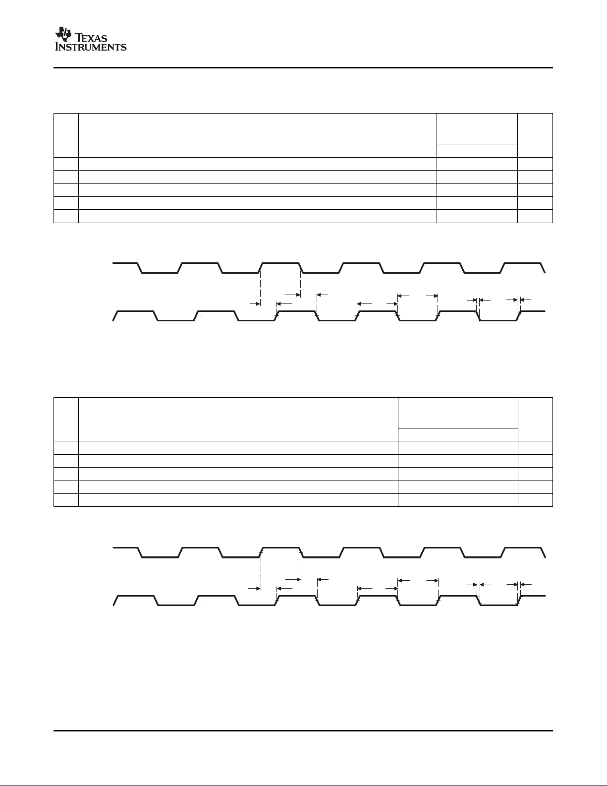
www.ti.com
4
5
1
2
AECLKIN
AECLKOUT1
3 3
4
5
1
2
AECLKIN
AECLKOUT2
3 3
Video/Imaging Fixed-Point Digital Signal Processor
SPRS200L – JULY 2002 – REVISED JANUARY 2007
TMS320DM642
Table 5-19. Switching Characteristics Over Recommended Operating Conditions for AECLKOUT1 for the
EMIFA Module
(1) (2) (3)
(see Figure 5-15 )
–500
NO. PARAMETER UNIT
–600
–720
MIN MAX
1 t
2 t
3 t
4 t
5 t
w(EKO1H)
w(EKO1L)
t(EKO1)
d(EKIH-EKO1H)
d(EKIL-EKO1L)
Pulse duration, AECLKOUT1 high EH – 0.7 EH + 0.7 ns
Pulse duration, AECLKOUT1 low EL – 0.7 EL + 0.7 ns
Transition time, AECLKOUT1 1 ns
Delay time, AECLKIN high to AECLKOUT1 high 1 8 ns
Delay time, AECLKIN low to AECLKOUT1 low 1 8 ns
(1) E = the EMIF input clock (AECLKIN, CPU/4 clock, or CPU/6 clock) period in ns for EMIFA.
(2) The reference points for the rise and fall transitions are measured at V
(3) EH is the high period of E (EMIF input clock period) in ns and EL is the low period of E (EMIF input clock period) in ns for EMIFA.
MAX and V
OL
MIN.
OH
Figure 5-15. AECLKOUT1 Timing for the EMIFA Module
Table 5-20. Switching Characteristics Over Recommended Operating Conditions for AECLKOUT2 for the
EMIFA Module
(1) (2)
(see Figure 5-16 )
–500
NO. PARAMETER UNIT
–600
–720
MIN MAX
1 t
w(EKO2H)
2 t
w(EKO2L)
3 t
t(EKO2)
4 t
d(EKIH-EKO2H)
5 t
d(EKIL-EKO2L)
(1) The reference points for the rise and fall transitions are measured at V
(2) E = the EMIF input clock (AECLKIN, CPU/4 clock, or CPU/6 clock) period in ns for EMIFA. N = the EMIF input clock divider; N = 1, 2,
Pulse duration, AECLKOUT2 high 0.5NE – 0.7 0.5NE + 0.7 ns
Pulse duration, AECLKOUT2 low 0.5NE – 0.7 0.5NE + 0.7 ns
Transition time, AECLKOUT2 1 ns
Delay time, AECLKIN high to AECLKOUT2 high 1 8 ns
Delay time, AECLKIN low to AECLKOUT2 low 1 8 ns
MAX and V
OL
MIN.
OH
or 4.
Figure 5-16. AECLKOUT2 Timing for the EMIFA Module
Submit Documentation Feedback DM642 Peripheral Information and Electrical Specifications 93

www.ti.com
TMS320DM642
Video/Imaging Fixed-Point Digital Signal Processor
SPRS200L – JULY 2002 – REVISED JANUARY 2007
5.8 External Memory Interface (EMIF)
EMIF supports a glueless interface to a variety of external devices, including:
• Pipelined synchronous-burst SRAM (SBSRAM)
• Synchronous DRAM (SDRAM)
• Asynchronous devices, including SRAM, ROM, and FIFOs
• An external shared-memory device
5.8.1 EMIF Device-Specific Information
EMIF Device Speed
The rated EMIF speed of these devices only applies to the SDRAM interface when in a system that meets
the following requirements:
• 1 chip-enable (CE) space (maximum of 2 chips) of SDRAM connected to EMIF
• up to 1 CE space of buffers connected to EMIF
• EMIF trace lengths between 1 and 3 inches
• 166-MHz SDRAM for 133-MHz operation
• 143-MHz SDRAM for 100-MHz operation
Other configurations may be possible, but timing analysis must be done to verify all AC timings are met.
Verification of AC timings is mandatory when using configurations other than those specified above. TI
recommends utilizing I/O buffer information specification (IBIS) to analyze all AC timings.
To properly use IBIS models to attain accurate timing analysis for a given system, see the Using IBIS
Models for Timing Analysis application report (literature number SPRA839).
To maintain signal integrity, serial termination resistors should be inserted into all EMIF output signal lines
(see the Terminal Functions table for the EMIF output signals).
For more detailed information on the DM642 EMIF peripheral, see the TMS320C6000 DSP External
Memory Interface (EMIF) Reference Guide (literature number SPRU266).
DM642 Peripheral Information and Electrical Specifications94 Submit Documentation Feedback
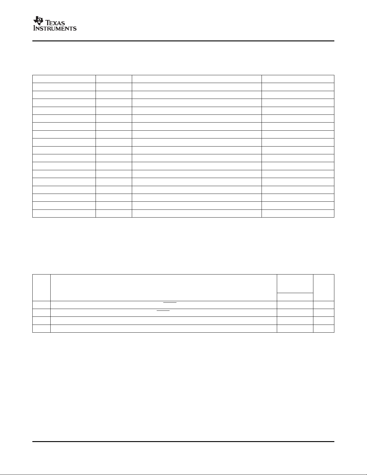
www.ti.com
Video/Imaging Fixed-Point Digital Signal Processor
SPRS200L – JULY 2002 – REVISED JANUARY 2007
5.8.2 EMIF Peripheral Register Description(s)
Table 5-21. EMIFA Registers
HEX ADDRESS RANGE ACRONYM REGISTER NAME COMMENTS
0180 0000 GBLCTL EMIFA global control
0180 0004 CECTL1 EMIFA CE1 space control
0180 0008 CECTL0 EMIFA CE0 space control
0180 000C – Reserved
0180 0010 CECTL2 EMIFA CE2 space control
0180 0014 CECTL3 EMIFA CE3 space control
0180 0018 SDCTL EMIFA SDRAM control
0180 001C SDTIM EMIFA SDRAM refresh control
0180 0020 SDEXT EMIFA SDRAM extension
0180 0024 – 0180 003C – Reserved
0180 0040 PDTCTL Peripheral device transfer (PDT) control
0180 0044 CESEC1 EMIFA CE1 space secondary control
0180 0048 CESEC0 EMIFA CE0 space secondary control
0180 004C – Reserved
0180 0050 CESEC2 EMIFA CE2 space secondary control
0180 0054 CESEC3 EMIFA CE3 space secondary control
0180 0058 – 0183 FFFF – Reserved
TMS320DM642
5.8.3 EMIF Electrical Data/Timing
5.8.3.1 Asynchronous Memory Timing
Table 5-22. Timing Requirements for Asynchronous Memory Cycles for EMIFA Module
(see Figure 5-17 and Figure 5-18 )
NO. UNIT
3 t
su(EDV-AREH)
4 t
h(AREH-EDV)
6 t
su(ARDY-EKO1H)
7 t
h(EKO1H-ARDY)
(1) To ensure data setup time, simply program the strobe width wide enough. AARDY is internally synchronized. The AARDY signal is only
recognized two cycles before the end of the programmed strobe time and while AARDY is low, the strobe time is extended
cycle-by-cycle. When AARDY is recognized low, the end of the strobe time is two cycles after AARDY is recognized high. To use
AARDY as an asynchronous input, the pulse width of the AARDY signal should be wide enough (e.g., pulse width = 2E) to ensure setup
and hold time is met.
(2) RS = Read setup, RST = Read strobe, RH = Read hold, WS = Write setup, WST = Write strobe, WH = Write hold. These parameters
are programmed via the EMIF CE space control registers.
Setup time, AEDx valid before AARE high 6.5 ns
Hold time, AEDx valid after AARE high 1 ns
Setup time, AARDY valid before AECLKOUTx high 3 ns
Hold time, AARDY valid after AECLKOUTx high 2.5 ns
(1) (2)
–500
–600
–720
MIN MAX
Submit Documentation Feedback DM642 Peripheral Information and Electrical Specifications 95

www.ti.com
7
7
66
Setup = 2 Strobe = 3 Not Ready Hold = 2
BE
Address
1
1
1
1
5
4
AARDY
5
AECLKOUTx
ACEx
AEA[22:3]
AED[63:0]
AAOE
/ASDRAS/ASOE
(A)
AARE/ASDCAS/ASADS/ASRE
(A)
ABE[7:0]
AAWE/ASDWE/ASWE
(A)
2
2
2
2
3
Read Data
TMS320DM642
Video/Imaging Fixed-Point Digital Signal Processor
SPRS200L – JULY 2002 – REVISED JANUARY 2007
Table 5-23. Switching Characteristics Over Recommended Operating Conditions for Asynchronous
Memory Cycles for EMIFA Module
(1) (2) (3)
(see Figure 5-17 and Figure 5-18 )
–500
NO. PARAMETER UNIT
–600
–720
MIN MAX
1 t
2 t
5 t
8 t
9 t
10 t
osu(SELV-AREL)
oh(AREH-SELIV)
d(EKO1H-AREV)
osu(SELV-AWEL)
oh(AWEH-SELIV)
d(EKO1H-AWEV)
Output setup time, select signals valid to AARE low RS * E – 1.8 ns
Output hold time, AARE high to select signals invalid RH * E – 1.9 ns
Delay time, AECLKOUTx high to AARE valid 1 7 ns
Output setup time, select signals valid to AAWE low WS * E – 2.0 ns
Output hold time, AAWE high to select signals invalid WH * E – 2.5 ns
Delay time, AECLKOUTx high to AAWE valid 1.3 7.1 ns
(1) RS = Read setup, RST = Read strobe, RH = Read hold, WS = Write setup, WST = Write strobe, WH = Write hold. These parameters
are programmed via the EMIF CE space control registers.
(2) E = AECLKOUT1 period in ns for EMIFA
(3) Select signals for EMIFA include: ACEx, ABE[7:0], AEA[22:3], AAOE; and for EMIFA writes, include AED[63:0].
A. AAOE/ ASDRAS/ ASOE, AARE/ ASDCAS/ ASADS/ ASRE, and AAWE/ ASDWE/ ASWE operate as AAOE (identified
under select signals), AARE, and AAWE, respectively, during asynchronous memory accesses.
DM642 Peripheral Information and Electrical Specifications96 Submit Documentation Feedback
Figure 5-17. Asynchronous Memory Read Timing for EMIFA

www.ti.com
Setup = 2
Strobe = 3 Not Ready
Hold = 2
BE
Address
Write Data
10
10
8
8
8
8
77
6
6
AECLKOUTx
ACEx
AEA[22:3]
AED[63:0]
ABE[7:0]
AARDY
AAOE/ASDRAS/ASOE
(A)
AARE/ASDCAS/ASADS/ASRE
(A)
AAWE/ASDWE/ASWE
(A)
9
9
9
9
Video/Imaging Fixed-Point Digital Signal Processor
SPRS200L – JULY 2002 – REVISED JANUARY 2007
TMS320DM642
A. AAOE/ ASDRAS/ ASOE, AARE/ ASDCAS/ ASADS/ ASRE, and AAWE/ ASDWE/ ASWE operate as AAOE (identified
under select signals), AARE, and AAWE, respectively, during asynchronous memory accesses.
Figure 5-18. Asynchronous Memory Write Timing for EMIFA
Submit Documentation Feedback DM642 Peripheral Information and Electrical Specifications 97

www.ti.com
TMS320DM642
Video/Imaging Fixed-Point Digital Signal Processor
SPRS200L – JULY 2002 – REVISED JANUARY 2007
5.8.3.2 Programmable Synchronous Interface Timing
Table 5-24. Timing Requirements for Programmable Synchronous Interface Cycles for EMIFA Module
(see Figure 5-19 )
NO. UNIT
–500, A-600
–600
–720
MIN MAX MIN MAX
6 t
su(EDV-EKOxH)
7 t
h(EKOxH-EDV)
Table 5-25. Switching Characteristics Over Recommended Operating Conditions for Programmable
Synchronous Interface Cycles for EMIFA Module
NO. PARAMETER UNIT
Setup time, read AEDx valid before AECLKOUTx high 3.1 2 ns
Hold time, read AEDx valid after AECLKOUTx high 1.8 1.5 ns
(1)
(see Figure 5-19 –Figure 5-21 )
–500, A-600
–600
–720
MIN MAX MIN MAX
1 t
2 t
3 t
4 t
5 t
8 t
9 t
10 t
11 t
12 t
d(EKOxH-CEV)
d(EKOxH-BEV)
d(EKOxH-BEIV)
d(EKOxH-EAV)
d(EKOxH-EAIV)
d(EKOxH-ADSV)
d(EKOxH-OEV)
d(EKOxH-EDV)
d(EKOxH-EDIV)
d(EKOxH-WEV)
Delay time, AECLKOUTx high to ACEx valid 1.1 6.4 1.1 4.9 ns
Delay time, AECLKOUTx high to ABEx valid 6.4 4.9 ns
Delay time, AECLKOUTx high to ABEx invalid 1.1 1.1 ns
Delay time, AECLKOUTx high to AEAx valid 6.4 4.9 ns
Delay time, AECLKOUTx high to AEAx invalid 1.1 1.1 ns
Delay time, AECLKOUTx high to ASADS/ ASRE valid 1.1 6.4 1.1 4.9 ns
Delay time, AECLKOUTx high to ASOE valid 1.1 6.4 1.1 4.9 ns
Delay time, AECLKOUTx high to AEDx valid 6.4 4.9 ns
Delay time, AECLKOUTx high to AEDx invalid 1.1 1.1 ns
Delay time, AECLKOUTx high to ASWE valid 1.1 6.4 1.1 4.9 ns
(1) The following parameters are programmable via the EMIF CE Space Secondary Control register (CExSEC):
• Read latency (SYNCRL): 0-, 1-, 2-, or 3-cycle read latency
• Write latency (SYNCWL): 0-, 1-, 2-, or 3-cycle write latency
• ACEx assertion length (CEEXT): For standard SBSRAM or ZBT SRAM interface, ACEx goes inactive after the final command has
been issued (CEEXT = 0). For synchronous FIFO interface with glue, ACEx is active when ASOE is active (CEEXT = 1).
• Function of ASADS/ ASRE (RENEN): For standard SBSRAM or ZBT SRAM interface, ASADS/ ASRE acts as ASADS with deselect
cycles (RENEN = 0). For FIFO interface, ASADS/ ASRE acts as ASRE with NO deselect cycles (RENEN = 1).
• Synchronization clock (SNCCLK): Synchronized to AECLKOUT1 or AECLKOUT2
DM642 Peripheral Information and Electrical Specifications98 Submit Documentation Feedback

www.ti.com
AECLKOUTx
ACEx
ABE[7:0]
AEA[22:3]
AED[63:0]
AARE/ASDCAS/ASADS/ASRE
(C)
AAOE/ASDRAS/ASOE
(C)
AAWE/ASDWE/ASWE
(C)
BE1 BE2 BE3 BE4
Q1 Q2 Q3 Q4
9
1
4
5
8
9
6
7
3
1
2
BE1 BE2 BE3 BE4
EA1 EA2
EA4
8
READ latency = 2
EA3
TMS320DM642
Video/Imaging Fixed-Point Digital Signal Processor
SPRS200L – JULY 2002 – REVISED JANUARY 2007
A. The read latency and the length of ACEx assertion are programmable via the SYNCRL and CEEXT fields,
respectively, in the EMIFA CE Space Secondary Control register (CExSEC). In this figure, SYNCRL = 2 and
CEEXT = 0.
B. The following parameters are programmable via the EMIF CE Space Secondary Control register (CExSEC):
• Read latency (SYNCRL): 0-, 1-, 2-, or 3-cycle read latency
• Write latency (SYNCWL): 0-, 1-, 2-, or 3-cycle write latency
• ACEx assertion length (CEEXT): For standard SBSRAM or ZBT SRAM interface, ACEx goes inactive after the
final command has been issued (CEEXT = 0). For synchronous FIFO interface with glue, ACEx is active when
ASOE is active (CEEXT = 1).
• Function of ASADS/ ASRE (RENEN): For standard SBSRAM or ZBT SRAM interface, ASADS/ ASRE acts as
ASADS with deselect cycles (RENEN = 0). For FIFO interface, ASADS/ ASRE acts as ASRE with NO deselect
cycles (RENEN = 1).
• Synchronization clock (SNCCLK): Synchronized to AECLKOUT1 or AECLKOUT2
C. AARE/ ASDCAS/ ASADS/ ASRE, AAOE/ ASDRAS/ ASOE, and AAWE/ ASDWE/ ASWE operate as ASADS/ ASRE,
ASOE, and ASWE, respectively, during programmable synchronous interface accesses.
Figure 5-19. Programmable Synchronous Interface Read Timing for EMIFA (With Read Latency = 2)
(A) (B)
Submit Documentation Feedback DM642 Peripheral Information and Electrical Specifications 99

www.ti.com
AECLKOUTx
ACEx
ABE[7:0]
AEA[22:3]
AED[63:0]
AARE
/ASDCAS/ASADS/ASRE
(C)
AAOE/ASDRAS/ASOE
(C)
AAWE/ASDWE/ASWE
(C)
BE1 BE2 BE3 BE4
Q1 Q2 Q3 Q4
12
11
3
1
12
10
4
2
1
8
5
8
EA1 EA2 EA3 EA4
10
TMS320DM642
Video/Imaging Fixed-Point Digital Signal Processor
SPRS200L – JULY 2002 – REVISED JANUARY 2007
A. The write latency and the length of ACEx assertion are programmable via the SYNCWL and CEEXT fields,
respectively, in the EMIFA CE Space Secondary Control register (CExSEC). In this figure, SYNCWL = 0 and
CEEXT = 0.
B. The following parameters are programmable via the EMIF CE Space Secondary Control register (CExSEC):
• Read latency (SYNCRL): 0-, 1-, 2-, or 3-cycle read latency
• Write latency (SYNCWL): 0-, 1-, 2-, or 3-cycle write latency
• ACEx assertion length (CEEXT): For standard SBSRAM or ZBT SRAM interface, ACEx goes inactive after the
final command has been issued (CEEXT = 0). For synchronous FIFO interface with glue, ACEx is active when
ASOE is active (CEEXT = 1).
• Function of ASADS/ ASRE (RENEN): For standard SBSRAM or ZBT SRAM interface, ASADS/ ASRE acts as
ASADS with deselect cycles (RENEN = 0). For FIFO interface, ASADS/ ASRE acts as ASRE with NO deselect
cycles (RENEN = 1).
• Synchronization clock (SNCCLK): Synchronized to AECLKOUT1 or AECLKOUT2
C. AARE/ ASDCAS/ ASADS/ ASRE, AAOE/ ASDRAS/ ASOE, and AAWE/ ASDWE/ ASWE operate as ASADS/ ASRE,
ASOE, and ASWE, respectively, during programmable synchronous interface accesses.
Figure 5-20. Programmable Synchronous Interface Write Timing for EMIFA (With Write Latency = 0)
(A) (B)
DM642 Peripheral Information and Electrical Specifications100 Submit Documentation Feedback
 Loading...