

TEXAS INSTRUMENTS TLV7211, TLV7211A Technical data
www.ti.com
FEATURES APPLICATIONS
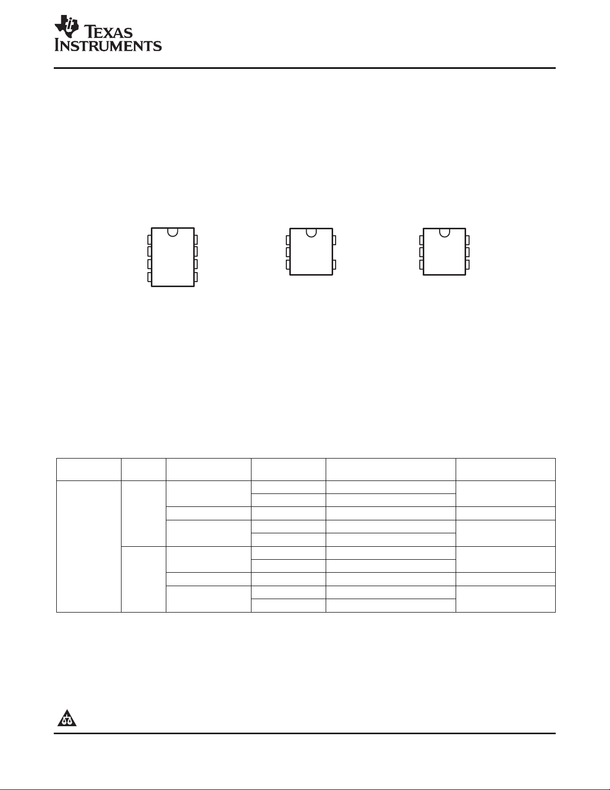
D PACKAGE
(TOPVIEW)
1
2
3
4
8
7
6
5
NC
V
CC+
OUT
NC
NC
IN–
IN+
V
CC–
NC – No internal connection
DBV PACKAGE
(TOPVIEW)
1
2
3
5
4
OUT
V
CC+
IN+
V
CC–
IN–
DCK PACKAGE
(TOPVIEW)
1
2
3
6
4
OUT
V
CC+
IN+
NC
IN–
5
V
CC–
• Parameters Specified at 2.7-V, 5-V, and 15-V
Supplies
• Supply Current 7 µ A (Typ) at 5 V
• Response Time 4 µ s (Typ) at 5 V
• Push-Pull Output
• Input Common-Mode Range Beyond
V
and V
CC–
• Low Input Current
CC+
TLV7211 , , TLV7211A
CMOS COMPARATORS
WITH RAIL-TO-RAIL INPUT AND PUSH-PULL OUTPUT
SLCS149B – AUGUST 2006 – REVISED JANUARY 2007
• Battery-Powered Products
• Notebooks and PDAs
• Mobile Communications
• Alarm and Security Circuits
• Direct Sensor Interface
• Replaces Amplifiers Used as Comparators
With Better Performance and Lower Current
DESCRIPTION/ORDERING INFORMATION
The TLV7211 and TLV7211A are micropower CMOS comparators available in the space-saving SOT-23-5
package. This makes the comparators ideal for space- and weight-critical designs. The TLV7211A features an
input offset voltage of 5 mV, and the TLV7211 features an input offset voltage of 15 mV.
The main benefits of the SOT-23-5 package are most apparent in small portable electronic devices, such as
mobile phones, pagers, notebook computers, personal digital assistants, and PCMCIA cards. The rail-to-rail
input voltage makes the TLV7211 or TLV7211A a good choice for sensor interfacing, such as light detector
circuits, optical and magnetic sensors, and alarm and status circuits.
The SOT-23-5 package's small size allows it to fit into tight spaces on PC boards.
ORDERING INFORMATION
V
T
A
–40 ° C to 85 ° C
(1) Package drawings, standard packing quantities, thermal data, symbolization, and PCB design guidelines are available at
www.ti.com/sc/package.
(2) DBV/DCK: The actual top-side marking has one additional character that designates the assembly/test site.
OS
(MAX)
5 mV SOT-23-5 – DBV Reel of 3000 TLV7211AIDBVR YBN_
15 mV SOT-23-5 – DBV Reel of 3000 TLV7211IDBVR YBK_
PACKAGE
SOIC – D 7211AI
SOT (SC-70) – DCK Y8_
SOIC – D TY7211
SOT (SC-70) – DCK Y7_
(1)
Reel of 2500 TLV7211AIDR
Tube of 75 TLV7211AID
Reel of 3000 TLV7211AIDCKR
Reel of 250 TLV7211AIDCKT
Reel of 2500 TLV7211IDR
Tube of 75 TLV7211ID
Reel of 3000 TLV7211IDCKR
Reel of 250 TLV7211IDCKT
ORDERABLE PART NUMBER TOP-SIDE MARKING
(2)
PRODUCTION DATA information is current as of publication date.
Products conform to specifications per the terms of the Texas
Instruments standard warranty. Production processing does not
necessarily include testing of all parameters.
Please be aware that an important notice concerning availability, standard warranty, and use in critical applications of Texas Instruments semiconductor products and disclaimers thereto appears at the end of this data sheet.
Copyright © 2006–2007, Texas Instruments Incorporated
www.ti.com
IN–
IN+
OUT
TLV7211 , , TLV7211A
CMOS COMPARATORS
WITH RAIL-TO-RAIL INPUT AND PUSH-PULL OUTPUT
SLCS149B – AUGUST 2006 – REVISED JANUARY 2007
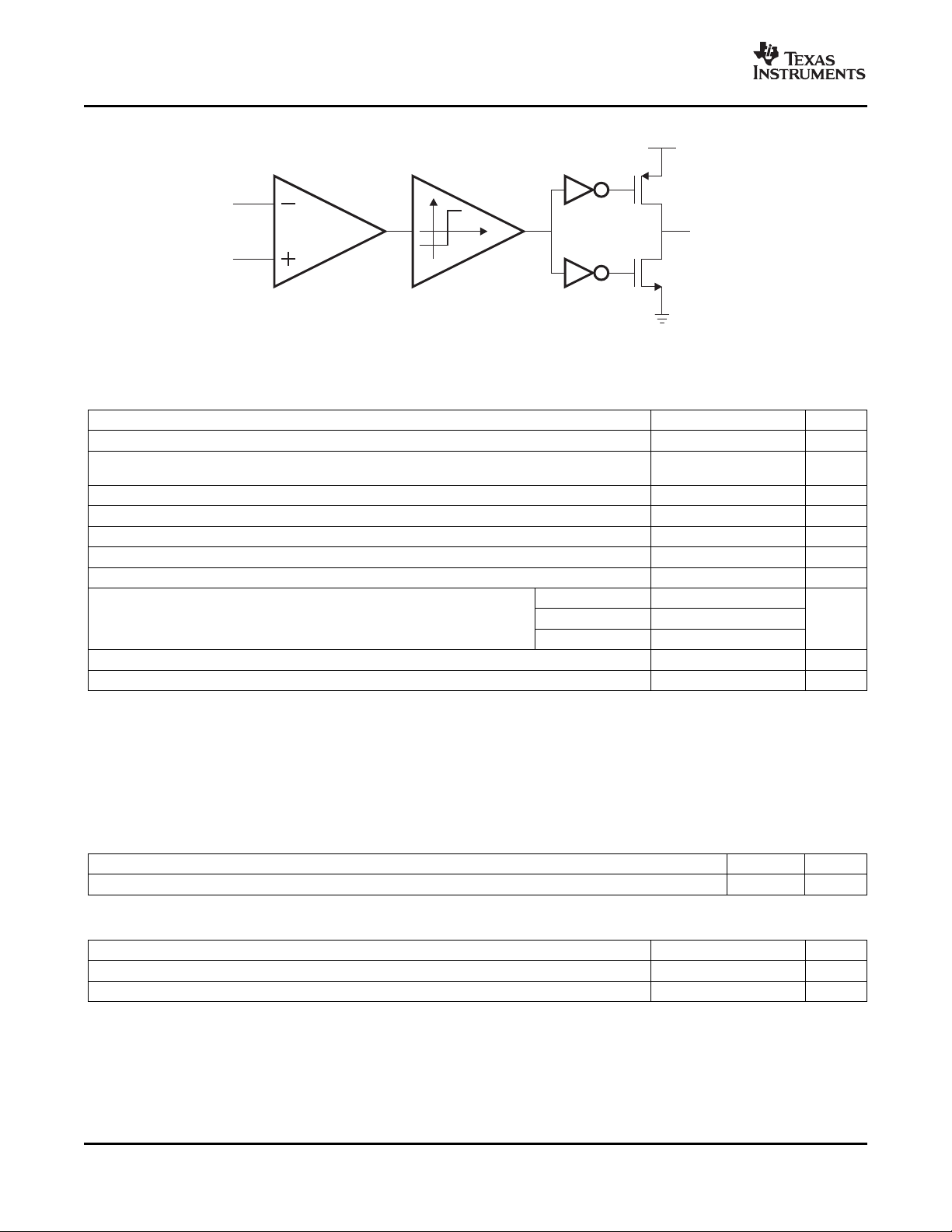
FUNCTIONAL BLOCK DIAGRAM
Absolute Maximum Ratings
(1)
over operating free-air temperature range (unless otherwise noted)
MIN MAX UNIT
V
– V
CC+
CC–
V
ID
V
I
V
O
I
CC
I
I
I
O
θ
JA
T
J
T
stg
Supply voltage
Differential input voltage
Input voltage range (any input) V
Output voltage range V
Supply current 40 mA
Input current ± 5 mA
Output current ± 30 mA
Package thermal impedance
Operating virtual junction temperature 150 ° C
Storage temperature range –65 150 ° C
(1) Stresses beyond those listed under "absolute maximum ratings" may cause permanent damage to the device. These are stress ratings
only, and functional operation of the device at these or any other conditions beyond those indicated under "recommended operating
conditions" is not implied. Exposure to absolute-maximum-rated conditions for extended periods may affect device reliability.
(2) All voltage values (except differential voltages and V
(3) Differential voltages are at IN+ with respect to IN–.
(4) Maximum power dissipation is a function of TJ(max), θJA, and TA. The maximum allowable power dissipation at any allowable ambient
temperature is PD= (TJ(max) – TA)/ θJA. Operating at the absolute maximum TJof 150 ° C can affect reliability.
(5) The package thermal impedance is calculated in accordance with JESD 51-7.
(2)
(3)
– 0.3 V
CC–
– 0.3 V
CC–
± Supply
voltage
CC+
CC+
+ 0.3 V
+ 0.3 V
D package 97
(4) (5)
DBV package 206 ° C/W
DCK package 259
specified for the measurement of IOS) are with respect to the network GND.
CC
16 V
V
ESD Protection
TYP UNIT
Human-Body Model 2000 V
Recommended Operating Conditions
MIN MAX UNIT
V
– V
CC+
CC–
T
J
2
Supply voltage 2.7 15 V
Operating virtual junction temperature –40 85 ° C
Submit Documentation Feedback
www.ti.com
TLV7211 , , TLV7211A
CMOS COMPARATORS
WITH RAIL-TO-RAIL INPUT AND PUSH-PULL OUTPUT
SLCS149B – AUGUST 2006 – REVISED JANUARY 2007
2.7-V Electrical Characteristics
V
= 2.7 V, V
CC+
PARAMETER TEST CONDITIONS T
V
OS
TCV
Input offset voltage mV
Input offset voltage
OS
temperature drift
Input offset voltage
average drift
I
B
I
OS
CMRR 0 ≤ V
PSRR 2.7 V ≤ V
A
V
CMVR V
V
OH
V
OL
I
CC
Input current 25 ° C 0.04 0.04 pA
Input offset current 25 ° C 0.02 0.02 pA
Common-mode
rejection ratio
Power-supply rejection
ratio
Voltage gain 25 ° C 100 100 dB
Input common-mode
voltage range
High-level output
voltage
Low-level output
voltage
Supply current µ A
(1) Input offset voltage average drift is calculated by dividing the accelerated operating life V
represents worst-case input conditions and includes the first 30 days of drift.
CC–
= GND, V
(1)
CM
= VO= V
/2, and RL> 1 M Ω (unless otherwise noted)
CC+
TLV7211A TLV7211
J
MIN TYP MAX MIN TYP MAX
25 ° C 3 5 3 15
–40 ° C to 85 ° C 8 18
25 ° C 1 1 µ V/ ° C
25 ° C 3.3 3.3 µ V/month
≤ 2.7 V 25 ° C 75 75 dB
CM
≤ 15 V 25 ° C 80 80 dB
CC+
CMRR > 55 dB
CMRR > 55 dB
I
= 2.5 mA V
load
I
= 2.5 mA V
load
V
= Low
OUT
V
= High-Idle
OUT
25 ° C 2.9 3 2.9 3
–40 ° C to 85 ° C 2.7 2.7
25 ° C –0.3 –0.2 –0.3 –0.2
–40 ° C to 85 ° C 0 0
25 ° C 2.4 2.5 2.4 2.5
–40 ° C to 85 ° C 2.3 2.3
25 ° C 0.2 0.3 0.2 0.3
–40 ° C to 85 ° C 0.4 0.4
25 ° C 7 12 7 12
–40 ° C to 85 ° C 14 14
25 ° C 5 10 5 10
–40 ° C to 85 ° C 12 12
drift by the equivalent operational time. This
OS
UNIT
Submit Documentation Feedback
3
www.ti.com
TLV7211 , , TLV7211A
CMOS COMPARATORS
WITH RAIL-TO-RAIL INPUT AND PUSH-PULL OUTPUT
SLCS149B – AUGUST 2006 – REVISED JANUARY 2007
5-V Electrical Characteristics
V
= 5 V, V
CC+
V
OS
TCV
OS
I
B
I
OS
CMRR 25 ° C 75 75 dB
PSRR 5 V ≤ V
A
V
CMVR V
V
OH
V
OL
I
CC
I
OH
I
OL
(1) Input offset voltage average drift is calculated by dividing the accelerated operating life V
represents worst-case input conditions and includes the first 30 days of drift.
(2) Do not short circuit the output to V+ if V+ is >12 V.
= GND, V
CC–
PARAMETER TEST CONDITIONS T
Input offset voltage mV
Input offset voltage
temperature drift
Input offset voltage
average drift
(1)
CM
= VO= V
/2, and RL> 1 M Ω (unless otherwise noted)
CC+
J
25 ° C 3 5 3 15
–40 ° C to 85 ° C 8 18
25 ° C 1 1 µ V/ ° C
25 ° C 3.3 3.3 µ V/month
TLV7211A TLV7211
MIN TYP MAX MIN TYP MAX
Input current 25 ° C 0.04 0.04 pA
Input offset current 25 ° C 0.02 0.02 pA
Common-mode
rejection ratio
Power-supply rejection
ratio
≤ 10 V 25 ° C 80 80 dB
CC+
Voltage gain 25 ° C 100 100 dB
Input common-mode
CMRR > 55 dB
voltage range
CMRR > 55 dB
High-level output
voltage
Low-level output
voltage
I
= 5 mA V
load
I
= 5 mA V
load
V
= Low
OUT
Supply current µ A
V
= High-Idle
OUT
Short-circuit output
current
Short-circuit output
current
I
source
I
sink
, VO< 12 V
(2)
25 ° C 5.2 5.3 5.2 5.3
–40 ° C to 85 ° C 5 5
25 ° C –0.3 –0.2 –0.3 –0.2
–40 ° C to 85 ° C 0 0
25 ° C 4.6 4.8 4.6 4.8
–40 ° C to 85 ° C 4.45 4.45
25 ° C 0.2 0.4 0.2 0.4
–40 ° C to 85 ° C 0.55 0.55
25 ° C 7 14 7 14
–40 ° C to 85 ° C 18 18
25 ° C 5 10 5 10
–40 ° C to 85 ° C 13 13
25 ° C 30 30 mA
25 ° C 45 45 mA
drift by the equivalent operational time. This
OS
UNIT
4
Submit Documentation Feedback
www.ti.com
TLV7211 , , TLV7211A
CMOS COMPARATORS
WITH RAIL-TO-RAIL INPUT AND PUSH-PULL OUTPUT
SLCS149B – AUGUST 2006 – REVISED JANUARY 2007
15-V Electrical Characteristics
V
= 15 V, V
CC+
V
TCV
Input offset voltage mV
OS
Input offset voltage
OS
temperature drift
Input offset voltage average
drift
I
B
I
OS
CMRR 25 ° C 82 82 dB
Input current 25 ° C 0.04 0.04 pA
Input offset current 25 ° C 0.02 0.02 pA
Common-mode rejection
ratio
PSRR Power-supply rejection ratio 5 V ≤ V
A
CMVR V
V
V
I
CC
I
OH
I
OL
Voltage gain 25 ° C 100 100 dB
V
Input common-mode voltage
range
High-level output voltage I
OH
Low-level output voltage I
OL
Supply current µ A
Short-circuit output current I
Short-circuit output current I
(1) Input offset voltage average drift is calculated by dividing the accelerated operating life V
represents worst-case input conditions and includes the first 30 days of drift.
(2) Do not short circuit the output to V+ if V+ is >12 V.
= GND, V
CC–
PARAMETER T
CM
= VO= V
/2, and RL> 1 M Ω (unless otherwise noted)
CC+
TEST
CONDITIONS
–40 ° C to 85 ° C 8 18
(1)
≤ 10 V 25 ° C 80 80 dB
CC+
CMRR > 55 dB
CMRR > 55 dB
= 5 mA V
load
= 5 mA V
load
V
= Low
OUT
V
= High-Idle
OUT
source
, VO< 12 V
sink
–40 ° C to 85 ° C 15 15
–40 ° C to 85 ° C 0 0
–40 ° C to 85 ° C 14.45 14.45
–40 ° C to 85 ° C 0.55 0.55
–40 ° C to 85 ° C 18 18
–40 ° C to 85 ° C 14 14
(2)
J
MIN TYP MAX MIN TYP MAX
25 ° C 3 5 3 15
25 ° C 4 4 µ V/ ° C
25 ° C 4 4 µ V/month
25 ° C 15.2 15.3 15.2 15.3
25 ° C –0.3 –0.2 –0.3 –0.2
25 ° C 14.6 14.8 14.6 14.8
25 ° C 0.2 0.4 0.2 0.4
25 ° C 7 14 7 14
25 ° C 5 12 5 12
25 ° C 30 30 mA
25 ° C 45 45 mA
drift by the equivalent operational time. This
OS
TLV7211A TLV7211
UNIT
Submit Documentation Feedback
5
 Loading...