

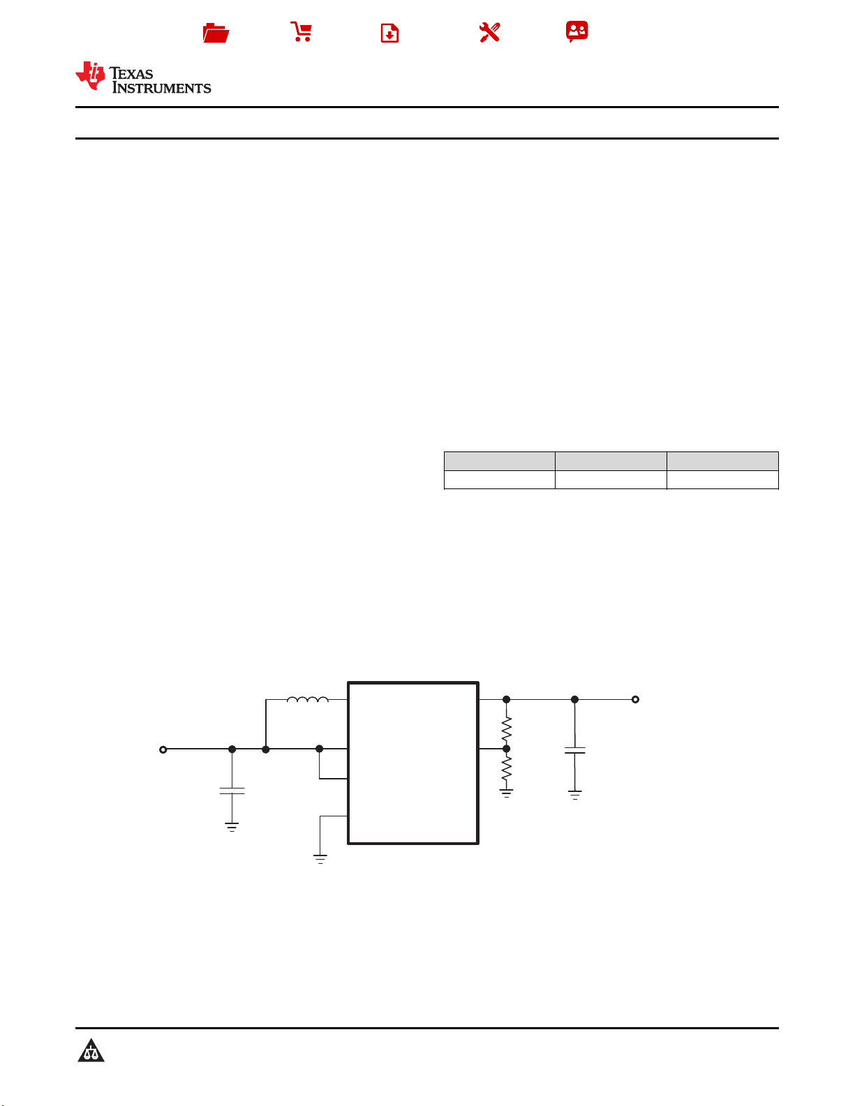
SW
L
1
4.7:H
VBAT
VOUT
FB
C
2
10 F:
EN
GND
TLV61220
V
OUT
R
1
R
2
V
IN
C
1
10 F:
0.7V to V
OUT
1.8V to 5.5V
Product
Folder
Sample &
Buy
Technical
Documents
Tools &
Software
Support &
Community
SLVSB53A –MAY 2012–REVISED DECEMBER 2014
TLV61220 Low-Input Voltage Step-Up Converter in Thin SOT-23 Package
1 Features 3 Description
1
• Up to 95% Efficiency at Typical Operating
Conditions
• 5.5-μA Quiescent Current
• Startup Into Load at 0.7-V Input Voltage
• Operating Input Voltage from 0.7 V to 5.5 V
• Pass-Through Function during Shutdown
• Minimum Switching Current 200 mA
• Protections:
– Output Overvoltage
– Overtemperature
– Input Undervoltage Lockout
• Adjustable Output Voltage from 1.8 V to 5.5 V
• Small 6-pin Thin SOT-23 Package
2 Applications
• Battery Powered Applications
– 1 to 3 Cell Alkaline, NiCd or NiMH
– 1 Cell Li-Ion or Li-Primary
• Solar or Fuel Cell Powered Applications
• Consumer and Portable Medical Products
• Personal Care Products
• White or Status LEDs
• Smartphones
The TLV61220 device provides a power-supply
solution for products powered by either a single-cell,
two-cell, or three-cell alkaline, NiCd or NiMH, or onecell Li-Ion or Li-polymer battery. Possible output
currents depend on the input-to-output voltage ratio.
The boost converter is based on a hysteretic
controller topology using synchronous rectification to
obtain maximum efficiency at minimal quiescent
currents. The output voltage of the adjustable version
can be programmed by an external resistor divider, or
is set internally to a fixed output voltage. The
converter can be switched off by a featured enable
pin. While being switched off, battery drain is
minimized. The device is packaged in a 6-pin thin
SOT-23 package (DBV).
spacer
Device Information
PART NUMBER PACKAGE BODY SIZE (NOM)
TLV61220 SOT (6) 2.90 mm x 1.60 mm
(1) For all available packages, see the orderable addendum at
the end of the datasheet.
TLV61220
(1)
4 Typical Application Schematic
1
An IMPORTANT NOTICE at the end of this data sheet addresses availability, warranty, changes, use in safety-critical applications,
intellectual property matters and other important disclaimers. PRODUCTION DATA.
TLV61220
SLVSB53A –MAY 2012–REVISED DECEMBER 2014
www.ti.com
Table of Contents
1 Features.................................................................. 1
2 Applications ........................................................... 1
3 Description ............................................................. 1
4 Typical Application Schematic............................. 1
5 Revision History..................................................... 2
6 Device Options....................................................... 3
7 Pin Configuration and Functions......................... 3
8 Specifications......................................................... 4
8.1 Absolute Maximum Ratings...................................... 4
8.2 ESD Ratings.............................................................. 4
8.3 Recommended Operating Conditions....................... 4
8.4 Thermal Information.................................................. 4
8.5 Electrical Characteristics........................................... 5
8.6 Typical Characteristics.............................................. 6
9 Parameter Measurement Information .................. 9
10 Detailed Description ........................................... 10
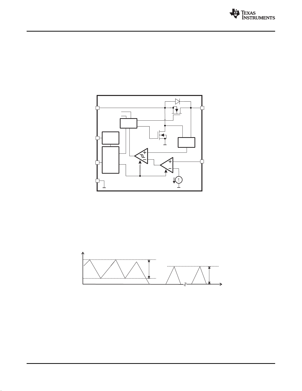
10.1 Overview ............................................................... 10
10.2 Functional Block Diagram..................................... 10
10.3 Feature Description............................................... 10
10.4 Device Functional Modes...................................... 11
11 Application and Implementation........................ 12
11.1 Application Information.......................................... 12
11.2 Typical Application ............................................... 12
12 Power Supply Recommendations ..................... 16
13 Layout................................................................... 16
13.1 Layout Guidelines ................................................. 16
13.2 Layout Example .................................................... 16
13.3 Thermal Considerations........................................ 16
14 Device and Documentation Support ................. 17
14.1 Device Support...................................................... 17
14.2 Documentation Support ........................................ 17
14.3 Trademarks........................................................... 17
14.4 Electrostatic Discharge Caution............................ 17
14.5 Glossary................................................................ 17
15 Mechanical, Packaging, and Orderable
Information........................................................... 17
5 Revision History
Changes from Original (May 2012) to Revision A Page
• Added ESD Ratings table, Feature Description section, Device Functional Modes, Application and Implementation
section, Power Supply Recommendations section, Layout section, Device and Documentation Support section, and
Mechanical, Packaging, and Orderable Information section.................................................................................................. 1
2 Submit Documentation Feedback Copyright © 2012–2014, Texas Instruments Incorporated
Product Folder Links: TLV61220
1 3
46
2
5
A B C
SW ENGND
VOUTVBAT FB
www.ti.com
6 Device Options
TLV61220
SLVSB53A –MAY 2012–REVISED DECEMBER 2014
T
A
–40°C to 85°C Adjustable 6-Pin SOT-23 TLV61220DBV
OUTPUT VOLTAGE
DC/DC
PACKAGE PART NUMBER
7 Pin Configuration and Functions
DBV Package
6 Pins
Top View
Pin Functions
PIN
NAME NO.
EN 3 I Enable input (VBAT enabled, GND disabled)
FB 4 I Voltage feedback for programming the output voltage
GND 2 — IC ground connection for logic and power
SW 1 I Boost and rectifying switch input
VBAT 6 I Supply voltage
VOUT 5 O Boost converter output
I/O DESCRIPTION
Copyright © 2012–2014, Texas Instruments Incorporated Submit Documentation Feedback 3
Product Folder Links: TLV61220
TLV61220
SLVSB53A –MAY 2012–REVISED DECEMBER 2014
www.ti.com
8 Specifications
8.1 Absolute Maximum Ratings
over operating free-air temperature range (unless otherwise noted)
V
IN
T
J
T
stg
(1) Stresses beyond those listed under Absolute Maximum Ratings may cause permanent damage to the device. These are stress ratings
only, which do not imply functional operation of the device at these or any other conditions beyond those indicated under Recommended
Operating Conditions. Exposure to absolute-maximum-rated conditions for extended periods may affect device reliability.
Input voltage on VBAT, SW, VOUT, EN, FB –0.3 7.5 V
Operating junction temperature –40 150 °C
Storage temperature –65 150 °C
8.2 ESD Ratings
Human-body model (HBM), per ANSI/ESDA/JEDEC JS-001
V
(ESD)
Electrostatic discharge V
Charged-device model (CDM), per JEDEC specification JESD22- ±1500
(2)
C101
(1) JEDEC document JEP155 states that 500-V HBM allows safe manufacturing with a standard ESD control process.
(2) JEDEC document JEP157 states that 250-V CDM allows safe manufacturing with a standard ESD control process.
8.3 Recommended Operating Conditions
V
T
T
Supply voltage at VIN 0.7 5.5 V
IN
Operating free air temperature range –40 85 °C
A
Operating virtual junction temperature range –40 125 °C
J
(1)
MIN MAX UNIT
VALUE UNIT
(1)
±2000
MIN NOM MAX UNIT
8.4 Thermal Information
TLV61220
THERMAL METRIC
R
θJA
R
θJC(top)
R
θJB
ψ
JT
ψ
JB
R
θJC(bot)
Junction-to-ambient thermal resistance 185.7
Junction-to-case (top) thermal resistance 124.3
Junction-to-board thermal resistance 31.3
Junction-to-top characterization parameter 22.9
Junction-to-board characterization parameter 30.8
Junction-to-case (bottom) thermal resistance N/A
(1) For more information about traditional and new thermal metrics, see the IC Package Thermal Metrics application report, SPRA953.
(1)
DBV UNIT
6 PINS
°C/W
4 Submit Documentation Feedback Copyright © 2012–2014, Texas Instruments Incorporated
Product Folder Links: TLV61220
TLV61220
www.ti.com
SLVSB53A –MAY 2012–REVISED DECEMBER 2014
8.5 Electrical Characteristics
over recommended free-air temperature range and over recommended input voltage range (typical at an ambient temperature
range of 25°C) (unless otherwise noted)
PARAMETER TEST CONDITIONS MIN TYP MAX UNIT
DC/DC STAGE
V
IN
V
IN
V
OUT
V
FB
I
LH
I
SW
R
DS(on)
I
Q
I
SD
I
LKG
I
FB
I
EN
CONTROL STAGE
V
IL
V
IH
V
IL
V
IH
V
UVLO
Input voltage range 0.7 5.5 V
Minimum input voltage at startup R
TLV61220 output voltage range VIN< V
≥ 150 Ω 0.7 V
Load
OUT
1.8 5.5 V
TLV61220 feedback voltage 483 500 513 mV
Inductor current ripple 200 mA
V
= 3.3 V, VIN= 1.2 V, TA= 25 °C 220 400 mA
OUT
switch current limit V
Rectifying switch on resistance,
HSD
Main switch on resistance, LSD
Line regulation VIN< V
Load regulation VIN< V
V
Quiescent
current
Shutdown
current
IN
V
OUT
V
IN
Leakage current into VOUT VEN= 0 V, VIN= 1.2 V, V
Leakage current into SW VEN= 0 V, VIN= 1.2 V, VSW= 1.2 V, V
TLV61220 Feedback input
current
= 3.3 V, TA= -40°C to 85 °C 180 400 mA
OUT
V
= 3.3 V, TA= 0°C to 85 °C 200 400 mA
OUT
V
= 3.3 V 1000 mΩ
OUT
V
= 5 V 700 mΩ
OUT
V
= 3.3 V 600 mΩ
OUT
V
= 5 V 550 mΩ
OUT
OUT
OUT
IO= 0 mA, VEN= VIN= 1.2 V, V
VEN= 0 V, VIN= 1.2 V, V
OUT
OUT
= 3.3 V
OUT
≥ V
IN
= 3.3 V 1 μA
≥ V
OUT
IN
0.5%
0.5%
0.5 0.9 μA
5 7.5 μA
0.2 0.5 μA
0.01 0.2 μA
VFB= 0.5 V 0.01 μA
EN input current Clamped on GND or VIN(VIN< 1.5 V) 0.005 0.1 μA
EN input low voltage VIN≤ 1.5 V V
EN input high voltage VIN≤ 1.5 V V
0.8 ×
V
IN
0.2 ×
V
IN
EN input low voltage 5 V > VIN> 1.5 V 0.4 V
EN input high voltage 5 V > VIN> 1.5 V 1.2 V
Undervoltage lockout threshold
for turn off
VINdecreasing 0.5 0.7 V
Overvoltage protection threshold 5.5 7.5 V
Overtemperature protection 140 °C
Overtemperature hysteresis 20 °C
Copyright © 2012–2014, Texas Instruments Incorporated Submit Documentation Feedback 5
Product Folder Links: TLV61220
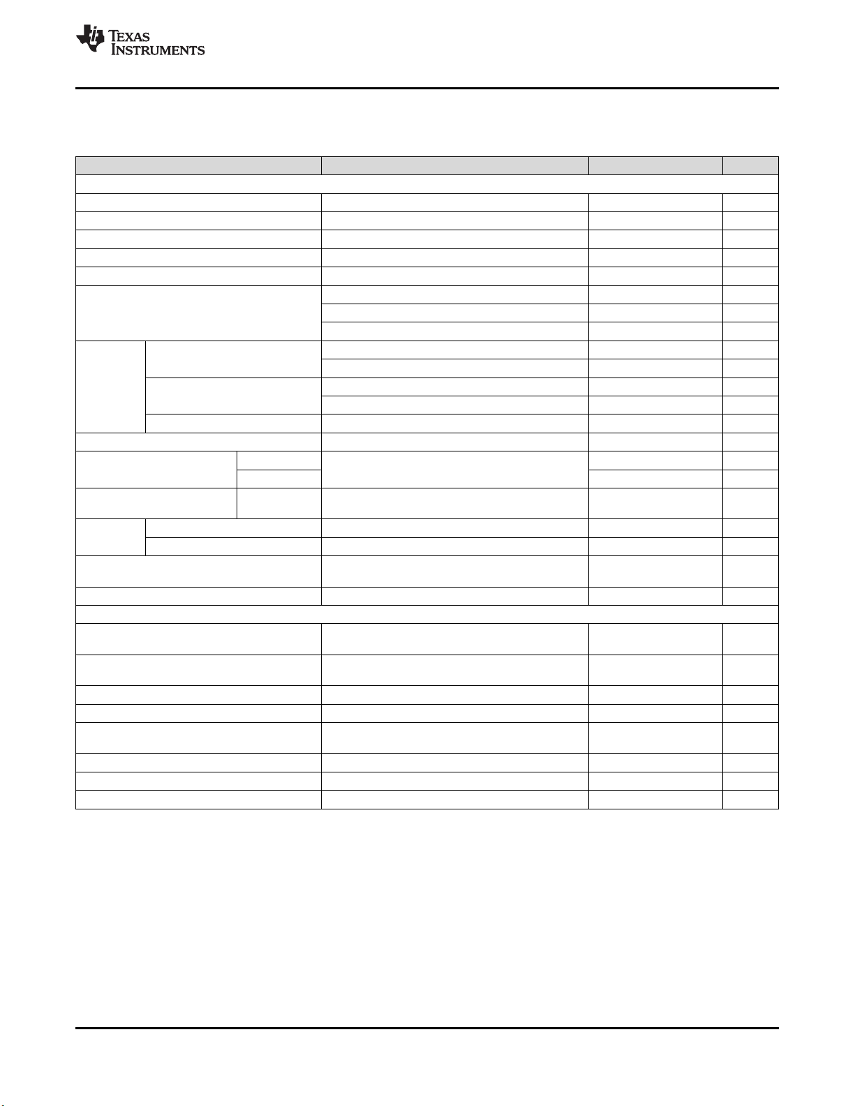
0
10
20
30
40
50
60
70
80
90
100
0.01 0.1 1 10 100
G000
Output Current - mA
Efficiency- %
V=0.7V
I
V=1.2V
I
V=1.5V
I
V =1.8V
o
Input Voltage - V
Output Current - A
Minimum I
SW
I =380mA
SW
0
0.03
0.06
0.09
0.12
0.15
0.18
0.21
0.24
0.27
1.0 1.5 2.0 2.5 3.0 3.5 4.0 4.5
Input Voltage - V
Output Current - A
Minimum I
SW
0
0.02
0.04
0.06
0.08
0.1
0.12
0.14
0.16
0.9 1.0 1.1 1.2 1.3 1.4
I =330mA
SW
Input Voltage - V
Output Current - A
Minimum I
SW
I =400mA
SW
0
0.03
0.06
0.09
0.12
0.15
0.18
0.21
0.24
0.27
0.7 1.2 1.7 2.2 2.7 3
TLV61220
SLVSB53A –MAY 2012–REVISED DECEMBER 2014
www.ti.com
8.6 Typical Characteristics
Table 1. Table of Graphs
FIGURE
Input Voltage, ISW= 330 mA, Minimum ISW= 200 mA, VO= 1.8V Figure 1
Output Current Input Voltage, ISW= 400 mA, Minimum ISW= 200 mA, VO= 3.3V Figure 2
Input Voltage, ISW= 380 mA, Minimum ISW= 200 mA, VO= 5V Figure 3
vs Output Current, VO= 1.8 V, VI= [0.7 V; 1.2 V; 1.5 V] Figure 4
Efficiency vs Output Current, VO= 3.3 V, VI= [0.7 V; 1.2 V; 2.4V; 3V] Figure 5
vs Output Current, VO= 5 V, VI= [0.7 V; 1.2 V; 3.6V; 4.2V] Figure 6
vs Input Voltage, VO= 1.8 V, IO= [100µA; 1mA ; 10mA; 50mA] Figure 7
Efficiency vs Input Voltage, VO= 3.3 V, IO= [100µA; 1mA ; 10mA; 50mA] Figure 8
vs Input Voltage, VO= 5 V, IO= [100µA; 1mA ; 10mA; 50mA] Figure 9
Output Voltage
vs Output Current, VO= 1.8 V, VI= [0.7 V; 1.2 V] Figure 10
vs Output Current, VO= 3.3 V, VI= [0.7 V; 1.2 V; 2.4 V] Figure 11
VO= 1.8 V
Figure 1. Maximum Output Current vs Input Voltage
6 Submit Documentation Feedback Copyright © 2012–2014, Texas Instruments Incorporated
VO= 5 V
Figure 3. Maximum Output Current vs Input Voltage
VO= 3.3 V
Figure 2. Maximum Output Current vs Input Voltage
Figure 4. Efficiency vs Output Current and Input Voltage
Product Folder Links: TLV61220
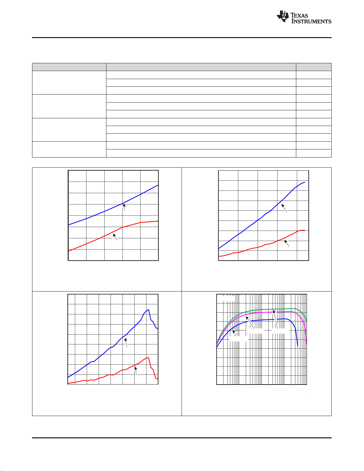
1.7
1.8
1.8
1.9
1.9
0.01 0.1 1 10 100
Output Current - mA
Output Voltage - V
V=0.7V
I
V=0.7V
I
V=0.7V
I
V=1.2V
I
V=0.7V
I
V =1.8V
o
Input Voltage - V
Efficiency - %
Io=100 A:
Io=50mA
Io=1mA
0
10
20
30
40
50
60
70
80
90
100
0.7 1.7 2.7 3.7 4.7 5.7
Io=1mA
Vo=5V
Io=50mA
Io=1mA
Io=10mA
Io=100 A:
Vo=1.8V
Input Voltage - V
Efficiency - %
0
10
20
30
40
50
60
70
80
90
100
0.7 0.9 1.1 1.3 1.5 1.7 1.9
Input Voltage - V
Efficiency - %
0
10
20
30
40
50
60
70
80
90
100
0.7 1.2 1.7 2.2 2.7 3.2 3.7
Io=100 A:
Io=50mA
Io=1mA
Io=10mA
Vo=3.3V
0
10
20
30
40
50
60
70
80
90
100
0.01 0.1 1 10 100
G000
Output Current - mA
Efficiency- %
V=0.7V
I
V=2.4V
I
V=0.7V
I
V=3V
I
V=1.2V
I
V =3.3V
o
0
10
20
30
40
50
60
70
80
90
100
0.01 0.1 1 10 100
G000
Output Current - mAOutput Current - mA
Efficiency - %
V=0.7V
I
V=0.7V
I
V=0.7V
I
V=3.6V
I
V=0.7V
I
V=0.7V
I
V=0.7V
I
V=4.2V
I
V=0.7V
I
V=0.7V
I
V=0.7V
I
V=1.2V
I
V =5V
o
www.ti.com
SLVSB53A –MAY 2012–REVISED DECEMBER 2014
Figure 5. Efficiency vs Output Current and Input Voltage Figure 6. Efficiency vs Input Voltage and Output Current
TLV61220
Figure 7. Efficiency vs Input Voltage and Output Current Figure 8. Efficiency vs Input Voltage and Output Current
Figure 9. Efficiency vs Input Voltage and Output Current
Copyright © 2012–2014, Texas Instruments Incorporated Submit Documentation Feedback 7
Figure 10. Output Voltage vs Output Current and Input
Voltage
Product Folder Links: TLV61220
Output Current - mA
Output Voltage - V
3.1
3.2
3.3
3.4
3.5
0.01 0.1 1 10 100
V=0.7V
I
V=1.2V
I
V=2.4V
I
V =3.3V
o
TLV61220
SLVSB53A –MAY 2012–REVISED DECEMBER 2014
Figure 11. Output Voltage vs Output Current and Input Voltage
www.ti.com
8 Submit Documentation Feedback Copyright © 2012–2014, Texas Instruments Incorporated
Product Folder Links: TLV61220

SW
L
1
4.7:H
VBAT
VOUT
FB
C
2
10 F:
EN
GND
TLV61220
V
OUT
R
1
R
2
V
IN
C
1
10 F:
0.7V to V
OUT
1.8V to 5.5V
www.ti.com
9 Parameter Measurement Information
Figure 12. Parameter Measurement Schematic
TLV61220
SLVSB53A –MAY 2012–REVISED DECEMBER 2014
Copyright © 2012–2014, Texas Instruments Incorporated Submit Documentation Feedback 9
Product Folder Links: TLV61220
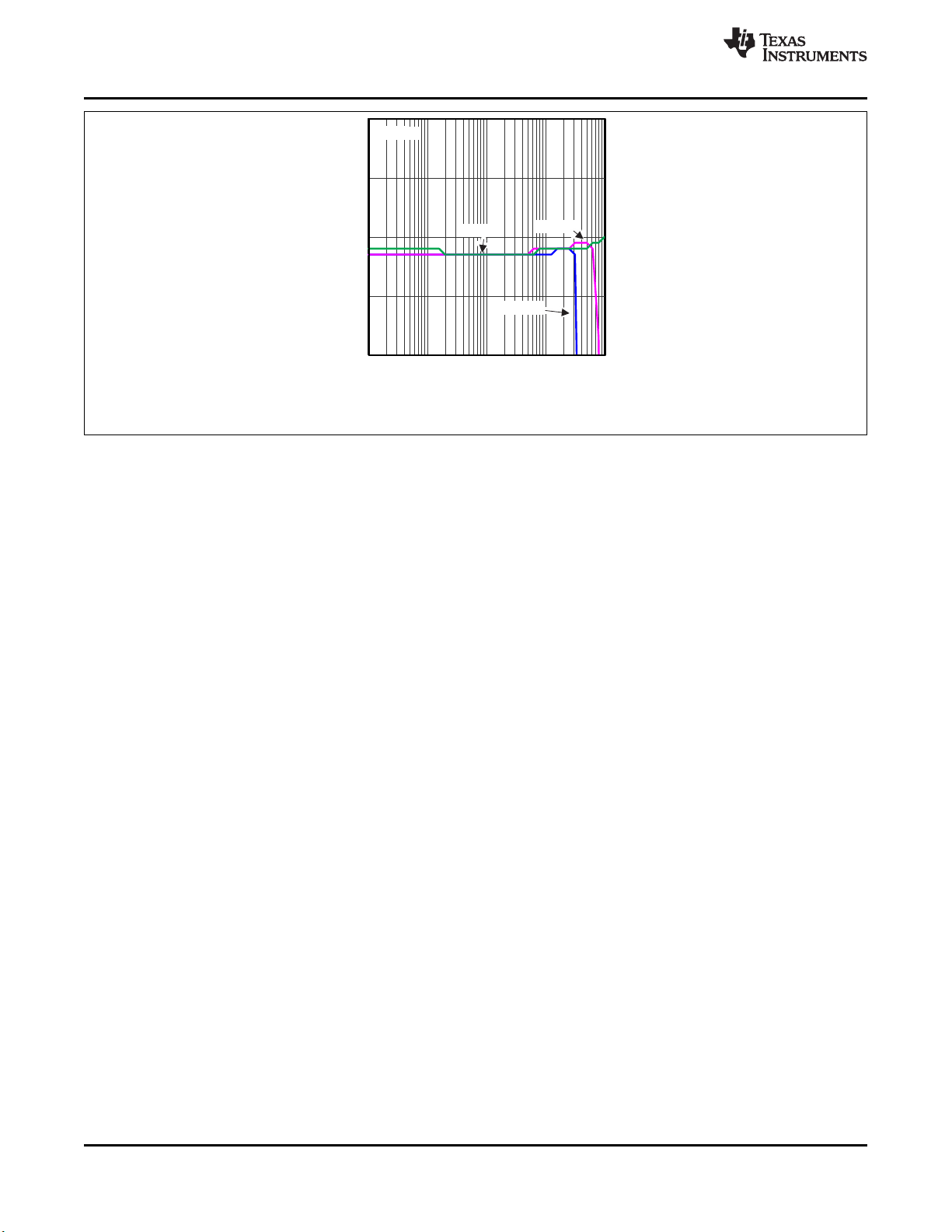
I
L
t
200mA
(typ.)
ContinuousCurrentOperation DiscontinuousCurrentOperation
200mA
(typ.)
Current
Sensor
Gate
Driver
Device
Control
GND
EN
FB
VOUT
SW
VREF
VBAT
Device
Control
Start Up
VIN
VOUT
TLV61220
SLVSB53A –MAY 2012–REVISED DECEMBER 2014
www.ti.com
10 Detailed Description
10.1 Overview
The TLV61220 is a high performance, highly efficient boost converter. To achieve high efficiency the power stage
is realized as a synchronous boost topology. For the power switching two actively controlled low R
MOSFETs are implemented.
10.2 Functional Block Diagram
DS(on)
power
10.3 Feature Description
10.3.1 Controller Circuit
The device is controlled by a hysteretic current mode controller. This controller regulates the output voltage by
keeping the inductor ripple current constant in the range of 200 mA and adjusting the offset of this inductor
current depending on the output load. In case the required average input current is lower than the average
inductor current defined by this constant ripple the inductor current gets discontinuous to keep the efficiency high
at low load conditions.
Figure 13. Hysteretic Current Operation
The output voltage V
To regulate the output voltage, the voltage error amplifier compares this feedback voltage to the internal voltage
reference and adjusts the required offset of the inductor current accordingly. An external resistor divider needs to
be connected.
The self oscillating hysteretic current mode architecture is inherently stable and allows fast response to load
variations. It also allows using inductors and capacitors over a wide value range.
is monitored via the feedback network which is connected to the voltage error amplifier.
OUT
10 Submit Documentation Feedback Copyright © 2012–2014, Texas Instruments Incorporated
Product Folder Links: TLV61220

TLV61220
www.ti.com
SLVSB53A –MAY 2012–REVISED DECEMBER 2014
Feature Description (continued)
10.3.1.1 Startup
After the EN pin is tied high, the device starts to operate. In case the input voltage is not high enough to supply
the control circuit properly a startup oscillator starts to operate the switches. During this phase the switching
frequency is controlled by the oscillator and the maximum switch current is limited. As soon as the device has
built up the output voltage to about 1.8 V, high enough for supplying the control circuit, the device switches to its
normal hysteretic current mode operation. The startup time depends on input voltage and load current.
10.3.1.2 Operation at Output Overload
If in normal boost operation the inductor current reaches the internal switch current limit threshold the main
switch is turned off to stop further increase of the input current.
In this case the output voltage will decrease since the device can not provide sufficient power to maintain the set
output voltage.
If the output voltage drops below the input voltage the backgate diode of the rectifying switch gets forward biased
and current starts flow through it. This diode cannot be turned off, so the current finally is only limited by the
remaining DC resistances. As soon as the overload condition is removed, the converter resumes providing the
set output voltage.
10.3.1.3 Undervoltage Lockout
An implemented undervoltage lockout function stops the operation of the converter if the input voltage drops
below the typical undervoltage lockout threshold. This function is implemented in order to prevent malfunctioning
of the converter.
10.3.1.4 Overvoltage Protection
If, for any reason, the output voltage is not fed back properly to the input of the voltage amplifier, control of the
output voltage will not work anymore. Therefore an overvoltage protection is implemented to avoid the output
voltage exceeding critical values for the device and possibly for the system it is supplying. For this protection the
TLV61220 output voltage is also monitored internally. In case it reaches the internally programmed threshold of
6.5 V typically the voltage amplifier regulates the output voltage to this value.
If the TLV61220 is used to drive LEDs, this feature protects the circuit if the LED fails.
10.3.1.5 Overtemperature Protection
The device has a built-in temperature sensor which monitors the internal IC junction temperature. If the
temperature exceeds the programmed threshold (see electrical characteristics table), the device stops operating.
As soon as the IC temperature has decreased below the programmed threshold, it starts operating again. To
prevent unstable operation close to the region of overtemperature threshold, a built-in hysteresis is implemented.
10.4 Device Functional Modes
10.4.1 Device Enable and Shutdown Mode
The device is enabled when EN is set high and shut down when EN is low. During shutdown, the converter stops
switching and all internal control circuitry is turned off. In this case the input voltage is connected to the output
through the back-gate diode of the rectifying MOSFET. This means that there always will be voltage at the output
which can be as high as the input voltage or lower depending on the load.
Copyright © 2012–2014, Texas Instruments Incorporated Submit Documentation Feedback 11
Product Folder Links: TLV61220

SW
L
1
4.7:H
VBAT
VOUT
FB
C
2
10 F:
EN
GND
TLV61220
V
OUT
R
1
1MS
R
2
V
IN
C
1
10 F:
1V to 3V
3.3V/20mA
180kS
TLV61220
SLVSB53A –MAY 2012–REVISED DECEMBER 2014
www.ti.com
11 Application and Implementation
NOTE
Information in the following applications sections is not part of the TI component
specification, and TI does not warrant its accuracy or completeness. TI’s customers are
responsible for determining suitability of components for their purposes. Customers should
validate and test their design implementation to confirm system functionality.
11.1 Application Information
The TLV61220 is intended for systems powered by a single cell battery to up to three Alkaline, NiCd or NiMH
cells with a typical terminal voltage between 0.7 V and 5.5 V. It can also be used in systems powered by one-cell
Li-Ion or Li-Polymer batteries with a typical voltage between 2.5 V and 4.2 V. Additionally, any other voltage
source with a typical output voltage between 0.7 V and 5.5 V can be used with the TLV61220.
11.2 Typical Application
Figure 14. Typical Application Circuit for Adjustable Output Voltage Option
11.2.1 Design Requirements
In this example, TLV61220 is used to design a 3.3-V power supply with up to 50-mA output current capability.
The TLV61220 can be powered by a single-cell battery to up to three Alkaline, NiCd or NiMH cells with a typical
terminal voltage between 0.7 V and 5.5 V. It can also be used in systems powered by one-cell Li-Ion or LiPolymer batteries with a typical voltage between 2.5 V and 4.2 V. In this example, the input voltage range is from
2 V to 3 V for one-cell coin cell battery input design.
Table 2. TLV61220 3.3 V Output Design Requirements
PARAMETERS VALUES
Input Voltage 2 V to 3 V
Output Voltage 3.3 V
Output Current 50 mA
11.2.2 Detailed Design Procedure Table 3. List of Components
COMPONENT
REFERENCE
C
1
C
2
L
1
R1, R
2
PART NUMBER MANUFACTURER VALUE
GRM188R60J106ME84D Murata 10 μF, 6.3V. X5R Ceramic
GRM188R60J106ME84D Murata 10 μF, 6.3V. X5R Ceramic
1269AS-H-4ZR7N Toko 4.7 μH
R1= 1MΩ, R2= Values depending on the programmed
output voltage
12 Submit Documentation Feedback Copyright © 2012–2014, Texas Instruments Incorporated
Product Folder Links: TLV61220

´
> ´
OUT OUT
IN
V I
0.8 100 mA
V
´
ì
ï
´
í
ï
î
OUT OUT
IN
L,MAX
V I
+ 100 mA; continous current operation
0.8 V
I =
200 mA; discontinuous current operation
´
´
´
IN OUT IN
OUT
V (V -V )
1
L =
f 200 mA V
æ ö
ç ÷
è ø
OUT
FB
V
R = R x - 1
1 2
V
TLV61220
www.ti.com
SLVSB53A –MAY 2012–REVISED DECEMBER 2014
11.2.2.1 Adjustable Output Voltage Version
An external resistor divider is used to adjust the output voltage. The resistor divider needs to be connected
between VOUT, FB and GND as shown in Figure 14. When the output voltage is regulated properly, the typical
voltage value at the FB pin is 500 mV. The maximum recommended value for the output voltage is 5.5 V. The
current through the resistive divider should be about 100 times greater than the current into the FB pin. The
typical current into the FB pin is 0.01 μA, and the voltage across the resistor between FB and GND, R2, is
typically 500 mV. Based on those two values, the recommended value for R2should be lower than 500 kΩ, in
order to set the divider current to 1 μA or higher. The value of the resistor connected between VOUT and FB, R1,
depending on the needed output voltage (V
), can be calculated using Equation 1:
OUT
(1)
As an example, if an output voltage of 3.3 V is needed, a 1-MΩ resistor is calculated for R1when for R2a 180-kΩ
has been selected.
11.2.2.2 Inductor Selection
To make sure that the TLV61220 can operate, a suitable inductor must be connected between pin VBAT and pin
SW. Inductor values of 4.7 μH show good performance over the whole input and output voltage range .
Choosing other inductance values affects the switching frequency f proportional to 1/L as shown in Equation 2.
(2)
Choosing inductor values higher than 4.7 μH can improve efficiency due to reduced switching frequency and,
therefore, with reduced switching losses. Using inductor values below 2.2 μH is not recommended.
Having selected an inductance value, the peak current for the inductor in steady state operation can be
calculated. Equation 3 gives the peak current estimate.
(3)
For selecting the inductor this would be the suitable value for the current rating. It also needs to be taken into
account that load transients and error conditions may cause higher inductor currents.
Equation 4 helps to estimate whether the device will work in continuous or discontinuous operation depending on
the operating points. As long as the inequation is true, continuous operation is typically established. If the
inequation becomes false, discontinous operation is typically established.
(4)
The following inductor series from different suppliers have been used with TLV61220 converters:
Table 4. List of Inductors
VENDOR INDUCTOR SERIES
Toko DFE252010C
Coilcraft
Murata LQH3NP
Taiyo Yuden NR3015
Wurth Elektronik WE-TPC Typ S
EPL3015
EPL2010
Copyright © 2012–2014, Texas Instruments Incorporated Submit Documentation Feedback 13
Product Folder Links: TLV61220

Output Current
10mA/div, DC
V = 1.2V, V I = 5mA to 20mA
IN OUTOUT
=3.3V,
Output Voltage
20mV/div, AC
V = 1.8V to 2.4V, V I = 30mA
IN OUTOUT
=3.3V,
Output Voltage
100mV/div, AC
Input Voltage
500mV/div, DC
³ ´
2
L
C
2
TLV61220
SLVSB53A –MAY 2012–REVISED DECEMBER 2014
www.ti.com
11.2.2.3 Capacitor Selection
11.2.2.3.1 Input Capacitor
At least a 10-μF input capacitor is recommended to improve transient behavior of the regulator and EMI behavior
of the total power supply circuit. A ceramic capacitor placed as close as possible to the VBAT and GND pins of
the IC is recommended.
11.2.2.3.2 Output Capacitor
For the output capacitor C2, it is recommended to use small ceramic capacitors placed as close as possible to
the VOUT and GND pins of the IC. If, for any reason, the application requires the use of large capacitors which
can not be placed close to the IC, the use of a small ceramic capacitor with an capacitance value of around
2.2μF in parallel to the large one is recommended. This small capacitor should be placed as close as possible to
the VOUT and GND pins of the IC.
A minimum capacitance value of 4.7 μF should be used, 10 μF are recommended. If the inductor value exceeds
4.7 μH, the value of the output capacitance value needs to be half the inductance value or higher for stability
reasons, see Equation 5.
(5)
The TLV61220 is not sensitive to the ESR in terms of stability. Using low ESR capacitors, such as ceramic
capacitors, is recommended anyway to minimize output voltage ripple. If heavy load changes are expected, the
output capacitor value should be increased to avoid output voltage drops during fast load transients.
11.2.3 Application Curves
FIGURE
Load transient, VI= 1.2 V, VO= 3.3 V, IO= 5mA to 20 mA Figure 15
Line transient, VI= 1.8 V to 2.4V, VO= 3.3 V, IO= 30 mA Figure 16
Startup after Enable, VI= 1.2 V, VO= 3.3 V, R
= 50 Ω Figure 17
LOAD
spacing
Figure 15. Load Transient Response
Figure 16. Line Transient Response
14 Submit Documentation Feedback Copyright © 2012–2014, Texas Instruments Incorporated
Product Folder Links: TLV61220

Enable Voltage
2V/div, DC
Output Voltage
1V/div, DC
Load Current
20mA/div, DC
Inductor Current
200mA/div, DC
V = 1.2V, V = 50INS
OUT LOAD
=3.3V, R
www.ti.com
TLV61220
SLVSB53A –MAY 2012–REVISED DECEMBER 2014
Figure 17. Start Up After Enable
Copyright © 2012–2014, Texas Instruments Incorporated Submit Documentation Feedback 15
Product Folder Links: TLV61220
SW
GND
EN FB
VOUT
VBAT
VBAT
GND
VOUT
C
IN
L
C
OUT
R1
R2
Top Bottom
TLV61220
SLVSB53A –MAY 2012–REVISED DECEMBER 2014
www.ti.com
12 Power Supply Recommendations
The power supply can be single-cell, two-cell, or three-cell alkaline, NiCd or NiMH, or one-cell Li-Ion or Lipolymer battery.
The input supply should be well regulated with the rating of TLV61220. If the input supply is located more than a
few inches from the device, additional bulk capacitance may be required in addition to the ceramic bypass
capacitors. An electrolytic or tantalum capacitor with a value of 47 µF is a typical choice.
13 Layout
13.1 Layout Guidelines
As for all switching power supplies, the layout is an important step in the design, especially at high peak currents
and high switching frequencies. If the layout is not carefully done, the regulator could show stability problems as
well as EMI problems. Therefore, use wide and short traces for the main current path and for the power ground
paths. The input and output capacitor, as well as the inductor should be placed as close as possible to the IC.
The feedback divider should be placed as close as possible to the control ground pin of the IC. To lay out the
ground, it is recommended to use short traces as well, separated from the power ground traces. This avoids
ground shift problems, which can occur due to superimposition of power ground current and control ground
current. Assure that the ground traces are connected close to the device GND pin.
13.2 Layout Example
13.3 Thermal Considerations
Implementation of integrated circuits in low-profile and fine-pitch surface-mount packages typically requires
special attention to power dissipation. Many system-dependent issues such as thermal coupling, airflow, added
heat sinks and convection surfaces, and the presence of other heat-generating components affect the powerdissipation limits of a given component.
Three basic approaches for enhancing thermal performance are listed below.
• Improving the power-dissipation capability of the PCB design
• Improving the thermal coupling of the component to the PCB
• Introducing airflow in the system
For more details on how to use the thermal parameters in the dissipation ratings table please check the Thermal
Characteristics Application Note (SZZA017) and the IC Package Thermal Metrics Application Note (SPRA953).
16 Submit Documentation Feedback Copyright © 2012–2014, Texas Instruments Incorporated
Figure 18. PCB Layout Recommendation
Product Folder Links: TLV61220

TLV61220
www.ti.com
SLVSB53A –MAY 2012–REVISED DECEMBER 2014
14 Device and Documentation Support
14.1 Device Support
14.1.1 Third-Party Products Disclaimer
TI'S PUBLICATION OF INFORMATION REGARDING THIRD-PARTY PRODUCTS OR SERVICES DOES NOT
CONSTITUTE AN ENDORSEMENT REGARDING THE SUITABILITY OF SUCH PRODUCTS OR SERVICES
OR A WARRANTY, REPRESENTATION OR ENDORSEMENT OF SUCH PRODUCTS OR SERVICES, EITHER
ALONE OR IN COMBINATION WITH ANY TI PRODUCT OR SERVICE.
14.2 Documentation Support
14.2.1 Related Documentation
For related documentation see the following:
• Thermal Characteristics Application Note, SZZA017
• IC Package Thermal Metrics Application Note, SPRA953
14.3 Trademarks
All trademarks are the property of their respective owners.
14.4 Electrostatic Discharge Caution
These devices have limited built-in ESD protection. The leads should be shorted together or the device placed in conductive foam
during storage or handling to prevent electrostatic damage to the MOS gates.
14.5 Glossary
SLYZ022 — TI Glossary.
This glossary lists and explains terms, acronyms, and definitions.
15 Mechanical, Packaging, and Orderable Information
The following pages include mechanical, packaging, and orderable information. This information is the most
current data available for the designated devices. This data is subject to change without notice and revision of
this document. For browser-based versions of this data sheet, refer to the left-hand navigation.
Copyright © 2012–2014, Texas Instruments Incorporated Submit Documentation Feedback 17
Product Folder Links: TLV61220

PACKAGE OPTION ADDENDUM
www.ti.com
PACKAGING INFORMATION
Orderable Device Status
TLV61220DBVR ACTIVE SOT-23 DBV 6 3000 Green (RoHS
TLV61220DBVT ACTIVE SOT-23 DBV 6 250 Green (RoHS
(1)
The marketing status values are defined as follows:
ACTIVE: Product device recommended for new designs.
LIFEBUY: TI has announced that the device will be discontinued, and a lifetime-buy period is in effect.
NRND: Not recommended for new designs. Device is in production to support existing customers, but TI does not recommend using this part in a new design.
PREVIEW: Device has been announced but is not in production. Samples may or may not be available.
OBSOLETE: TI has discontinued the production of the device.
Package Type Package
(1)
Drawing
Pins Package
Qty
Eco Plan
(2)
& no Sb/Br)
& no Sb/Br)
Lead/Ball Finish
(6)
CU NIPDAU Level-1-260C-UNLIM -40 to 85 VUAI
CU NIPDAU Level-1-260C-UNLIM -40 to 85 VUAI
MSL Peak Temp
(3)
Op Temp (°C) Device Marking
(4/5)
(2)
Eco Plan - The planned eco-friendly classification: Pb-Free (RoHS), Pb-Free (RoHS Exempt), or Green (RoHS & no Sb/Br) - please check http://www.ti.com/productcontent for the latest availability
information and additional product content details.
TBD: The Pb-Free/Green conversion plan has not been defined.
Pb-Free (RoHS): TI's terms "Lead-Free" or "Pb-Free" mean semiconductor products that are compatible with the current RoHS requirements for all 6 substances, including the requirement that
lead not exceed 0.1% by weight in homogeneous materials. Where designed to be soldered at high temperatures, TI Pb-Free products are suitable for use in specified lead-free processes.
Pb-Free (RoHS Exempt): This component has a RoHS exemption for either 1) lead-based flip-chip solder bumps used between the die and package, or 2) lead-based die adhesive used between
the die and leadframe. The component is otherwise considered Pb-Free (RoHS compatible) as defined above.
Green (RoHS & no Sb/Br): TI defines "Green" to mean Pb-Free (RoHS compatible), and free of Bromine (Br) and Antimony (Sb) based flame retardants (Br or Sb do not exceed 0.1% by weight
in homogeneous material)
(3)
MSL, Peak Temp. - The Moisture Sensitivity Level rating according to the JEDEC industry standard classifications, and peak solder temperature.
(4)
There may be additional marking, which relates to the logo, the lot trace code information, or the environmental category on the device.
(5)
Multiple Device Markings will be inside parentheses. Only one Device Marking contained in parentheses and separated by a "~" will appear on a device. If a line is indented then it is a continuation
of the previous line and the two combined represent the entire Device Marking for that device.
(6)
Lead/Ball Finish - Orderable Devices may have multiple material finish options. Finish options are separated by a vertical ruled line. Lead/Ball Finish values may wrap to two lines if the finish
value exceeds the maximum column width.
Important Information and Disclaimer:The information provided on this page represents TI's knowledge and belief as of the date that it is provided. TI bases its knowledge and belief on information
provided by third parties, and makes no representation or warranty as to the accuracy of such information. Efforts are underway to better integrate information from third parties. TI has taken and
continues to take reasonable steps to provide representative and accurate information but may not have conducted destructive testing or chemical analysis on incoming materials and chemicals.
TI and TI suppliers consider certain information to be proprietary, and thus CAS numbers and other limited information may not be available for release.
6-Aug-2014
Samples
Addendum-Page 1

PACKAGE OPTION ADDENDUM
www.ti.com
In no event shall TI's liability arising out of such information exceed the total purchase price of the TI part(s) at issue in this document sold by TI to Customer on an annual basis.
6-Aug-2014
Addendum-Page 2

PACKAGE MATERIALS INFORMATION
www.ti.com 6-Aug-2014
TAPE AND REEL INFORMATION
*All dimensions are nominal
Device Package
Type
TLV61220DBVR SOT-23 DBV 6 3000 178.0 9.0 3.23 3.17 1.37 4.0 8.0 Q3
TLV61220DBVT SOT-23 DBV 6 250 178.0 9.0 3.23 3.17 1.37 4.0 8.0 Q3
Package
Drawing
Pins SPQ Reel
Diameter
(mm)
Reel
Width
W1 (mm)
A0
(mm)B0(mm)K0(mm)P1(mm)W(mm)
Pin1
Quadrant
Pack Materials-Page 1

PACKAGE MATERIALS INFORMATION
www.ti.com 6-Aug-2014
*All dimensions are nominal
Device Package Type Package Drawing Pins SPQ Length (mm) Width (mm) Height (mm)
TLV61220DBVR SOT-23 DBV 6 3000 180.0 180.0 18.0
TLV61220DBVT SOT-23 DBV 6 250 180.0 180.0 18.0
Pack Materials-Page 2


IMPORTANT NOTICE
Texas Instruments Incorporated and its subsidiaries (TI) reserve the right to make corrections, enhancements, improvements and other
changes to its semiconductor products and services per JESD46, latest issue, and to discontinue any product or service per JESD48, latest
issue. Buyers should obtain the latest relevant information before placing orders and should verify that such information is current and
complete. All semiconductor products (also referred to herein as “components”) are sold subject to TI’s terms and conditions of sale
supplied at the time of order acknowledgment.
TI warrants performance of its components to the specifications applicable at the time of sale, in accordance with the warranty in TI’s terms
and conditions of sale of semiconductor products. Testing and other quality control techniques are used to the extent TI deems necessary
to support this warranty. Except where mandated by applicable law, testing of all parameters of each component is not necessarily
performed.
TI assumes no liability for applications assistance or the design of Buyers’ products. Buyers are responsible for their products and
applications using TI components. To minimize the risks associated with Buyers’ products and applications, Buyers should provide
adequate design and operating safeguards.
TI does not warrant or represent that any license, either express or implied, is granted under any patent right, copyright, mask work right, or
other intellectual property right relating to any combination, machine, or process in which TI components or services are used. Information
published by TI regarding third-party products or services does not constitute a license to use such products or services or a warranty or
endorsement thereof. Use of such information may require a license from a third party under the patents or other intellectual property of the
third party, or a license from TI under the patents or other intellectual property of TI.
Reproduction of significant portions of TI information in TI data books or data sheets is permissible only if reproduction is without alteration
and is accompanied by all associated warranties, conditions, limitations, and notices. TI is not responsible or liable for such altered
documentation. Information of third parties may be subject to additional restrictions.
Resale of TI components or services with statements different from or beyond the parameters stated by TI for that component or service
voids all express and any implied warranties for the associated TI component or service and is an unfair and deceptive business practice.
TI is not responsible or liable for any such statements.
Buyer acknowledges and agrees that it is solely responsible for compliance with all legal, regulatory and safety-related requirements
concerning its products, and any use of TI components in its applications, notwithstanding any applications-related information or support
that may be provided by TI. Buyer represents and agrees that it has all the necessary expertise to create and implement safeguards which
anticipate dangerous consequences of failures, monitor failures and their consequences, lessen the likelihood of failures that might cause
harm and take appropriate remedial actions. Buyer will fully indemnify TI and its representatives against any damages arising out of the use
of any TI components in safety-critical applications.
In some cases, TI components may be promoted specifically to facilitate safety-related applications. With such components, TI’s goal is to
help enable customers to design and create their own end-product solutions that meet applicable functional safety standards and
requirements. Nonetheless, such components are subject to these terms.
No TI components are authorized for use in FDA Class III (or similar life-critical medical equipment) unless authorized officers of the parties
have executed a special agreement specifically governing such use.
Only those TI components which TI has specifically designated as military grade or “enhanced plastic” are designed and intended for use in
military/aerospace applications or environments. Buyer acknowledges and agrees that any military or aerospace use of TI components
which have not been so designated is solely at the Buyer's risk, and that Buyer is solely responsible for compliance with all legal and
regulatory requirements in connection with such use.
TI has specifically designated certain components as meeting ISO/TS16949 requirements, mainly for automotive use. In any case of use of
non-designated products, TI will not be responsible for any failure to meet ISO/TS16949.
Products Applications
Audio www.ti.com/audio Automotive and Transportation www.ti.com/automotive
Amplifiers amplifier.ti.com Communications and Telecom www.ti.com/communications
Data Converters dataconverter.ti.com Computers and Peripherals www.ti.com/computers
DLP® Products www.dlp.com Consumer Electronics www.ti.com/consumer-apps
DSP dsp.ti.com Energy and Lighting www.ti.com/energy
Clocks and Timers www.ti.com/clocks Industrial www.ti.com/industrial
Interface interface.ti.com Medical www.ti.com/medical
Logic logic.ti.com Security www.ti.com/security
Power Mgmt power.ti.com Space, Avionics and Defense www.ti.com/space-avionics-defense
Microcontrollers microcontroller.ti.com Video and Imaging www.ti.com/video
RFID www.ti-rfid.com
OMAP Applications Processors www.ti.com/omap TI E2E Community e2e.ti.com
Wireless Connectivity www.ti.com/wirelessconnectivity
Mailing Address: Texas Instruments, Post Office Box 655303, Dallas, Texas 75265
Copyright © 2015, Texas Instruments Incorporated

 Loading...