

TLV1572
2.7 V TO 5.5 V, 10-BIT, 1.25 MSPS
SERIAL ANALOG-TO-DIGITAL CONVERTER WITH AUTO-POWERDOWN
SLAS171A – DECEMBER 1997– REVISED SEPTEMBER 1998
1
POST OFFICE BOX 655303 • DALLAS, TEXAS 75265
D
Fast Throughput Rate: 1.25 MSPS
D
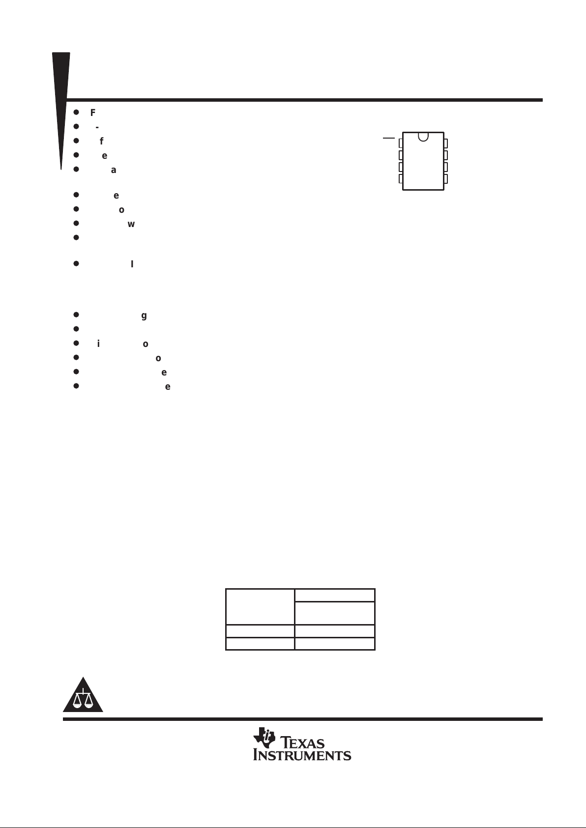
8-Pin SOIC Package
D
Differential Nonlinearity Error: < ±1 LSB
D
Integral Nonlinearity Error: < ±1 LSB
D
Signal-to-Noise and Distortion Ratio: 59 dB,
f
(input)
= 500 kHz
D
Single 3-V to 5-V Supply Operation
D
Very Low Power: 8 mW at 3V; 25mW at 5 V
D
Auto-Powerdown: 10 µA Maximum
D
Glueless Serial Interface to TMS320 DSPs
and (Q)SPI Compatible Micro-Controllers
D
Inherent Internal Sample and Hold
Operation
Applications
D
Mass Storage and HDD
D
Automotive
D
Digital Servos
D
Process Control
D
General Purpose DSP
D
Contact Image Sensor Processing
description
The TL V1572 is a high-speed 10-bit successive-approximation analog-to-digital converter (ADC) that operates
from a single 2.7-V to 5.5-V power supply and is housed in a small 8-pin SOIC package.
The TL V1572 accepts an analog input range from 0 to V
CC
and digitizes the input at a maximum 1.25 MSPS
throughput rate. The power dissipation is only 8 mW with a 3-V supply or 25 mW with a 5-V supply . The device
features an auto-powerdown mode that automatically powers down to 10 µA whenever a conversion is not
performed.
The TLV1572 communicates with digital microprocessors via a simple 3- or 4-wire serial port that interfaces
directly to the Texas Instruments TMS320 DSPs and (Q)SPI compatible microcontrollers without using
additional glue logic.
Very high throughput rate, simple serial interface, SO-8 package, 3-V operation, and low power consumption
make the TLV1572 an ideal choice for compact or remote high-speed systems.
AVAILABLE OPTIONS
PACKAGE
T
A
SMALL OUTLINE
(D)
0°C to 70°C TLV1572CD
–40°C to 85°C TLV1572ID
Copyright 1998, Texas Instruments Incorporated
PRODUCTION DATA information is current as of publication date.
Products conform to specifications per the terms of Texas Instruments
standard warranty. Production processing does not necessarily include
testing of all parameters.
Please be aware that an important notice concerning availability, standard warranty, and use in critical applications of
Texas Instruments semiconductor products and disclaimers thereto appears at the end of this data sheet.
1
2
3
4
8
7
6
5
CS
VREF
GND
AIN
DO
FS
V
CC
SCLK
D PACKAGE
(TOP VIEW)
TLV1572
2.7 V TO 5.5 V, 10-BIT, 1.25 MSPS
SERIAL ANALOG-TO-DIGITAL CONVERTER WITH AUTO-POWERDOWN
SLAS171A – DECEMBER 1997– REVISED SEPTEMBER 1998
2
POST OFFICE BOX 655303 • DALLAS, TEXAS 75265
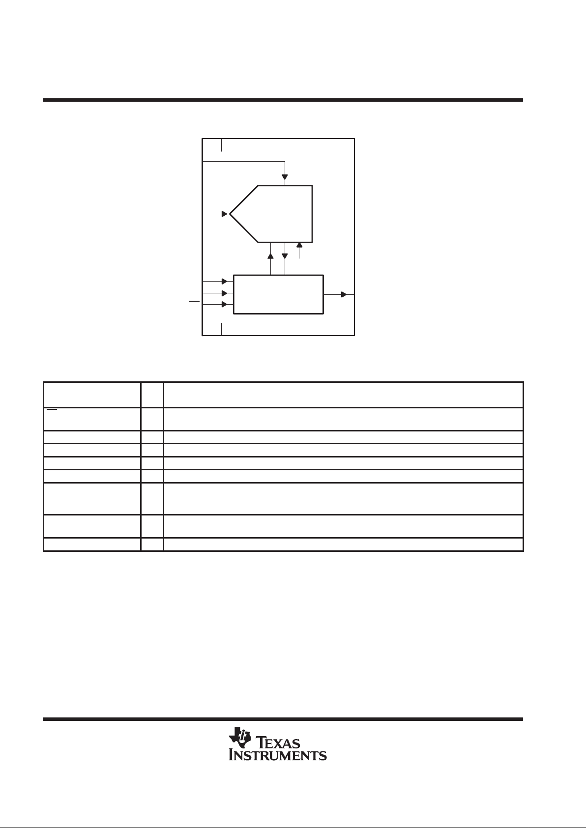
functional block diagram
AIN
SCLK
FS
CS
DO
10-BIT
SAR ADC
CONTROL LOGIC
V
CC
GND
VREF
GND
VREF
Terminal Functions
TERMINAL
NAME NO.
I/O
DESCRIPTION
CS/Powerdown 1 I Chip Select. A low on this input enables the TLV1572. A high disables the device and disconnects the power
to the TLV1572.
AIN 2 I Analog input
V
REF
3 I Reference voltage input. The voltage applied to this pin defines the input span of the TLV1572.
GND 4 Ground
DO 5 O Serial data output. A/D conversion results are provided at this output pin.
FS 6 I Frame sync input in DSP mode. The falling edge of the frame sync pulse from DSP indicates the start of
a serial data frame shifted out of the TLV1572. The FS input is tied to VCC when interfacing to a
micro-controller.
SCLK 7 I Serial clock input. This clock synchronizes the serial data transfer and is also used for internal data
conversion.
V
CC
8 Power supply, recommend connection to analog supply
TLV1572
2.7 V TO 5.5 V, 10-BIT, 1.25 MSPS
SERIAL ANALOG-TO-DIGITAL CONVERTER WITH AUTO-POWERDOWN
SLAS171A – DECEMBER 1997– REVISED SEPTEMBER 1998
3
POST OFFICE BOX 655303 • DALLAS, TEXAS 75265
absolute maximum ratings over operating free-air temperature (unless otherwise noted)
†
Supply voltage, GND to V
CC
–0.3 V to 6.5 V. . . . . . . . . . . . . . . . . . . . . . . . . . . . . . . . . . . . . . . . . . . . . . . . . . . . . . .
Analog input voltage range –0.3 V to V
CC
+ 0.3 V. . . . . . . . . . . . . . . . . . . . . . . . . . . . . . . . . . . . . . . . . . . . . . . . . .
Reference input voltage V
CC
+ 0.3 V. . . . . . . . . . . . . . . . . . . . . . . . . . . . . . . . . . . . . . . . . . . . . . . . . . . . . . . . . . . . .
Digital input voltage range –0.3 V to V
CC
+ 0.3 V. . . . . . . . . . . . . . . . . . . . . . . . . . . . . . . . . . . . . . . . . . . . . . . . . .
Operating
virtual junction temperature range, T
J
–40°C to 150°C. . . . . . . . . . . . . . . . . . . . . . . . . . . . . . . . . . . .
Operating free-air temperature range, T
A
0°C to 70°C. . . . . . . . . . . . . . . . . . . . . . . . . . . . . . . . . . . . . . . . . . . . . .
Storage temperature range, T
stg
–65°C to 150°C. . . . . . . . . . . . . . . . . . . . . . . . . . . . . . . . . . . . . . . . . . . . . . . . . . .
Lead temperature 1.6 mm (1/16 inch) from case for 10 seconds 260°C. . . . . . . . . . . . . . . . . . . . . . . . . . . . . . .
†
Stresses beyond those listed under “absolute maximum ratings” may cause permanent damage to the device. These are stress ratings only, and
functional operation of the device at these or any other conditions beyond those indicated under “recommended operating conditions” is not
implied. Exposure to absolute-maximum-rated conditions for extended periods may affect device reliability.
recommended operating conditions
power supply
MIN NOM MAX UNIT
V
CC
Supply voltage 2.7 5.5 V
analog inputs
MIN MAX UNIT
V
AIN
Analog input voltage GND V
REF
V
V
REF
Reference input voltage 2.7 V
CC
V
digital inputs
MIN NOM MAX UNIT
High-level input voltage, V
IH
VCC = 3 V to 5.5 V 2.1 2.4 V
Low-level input voltage, V
IL
VCC = 3 V to 5.5 V 0.8 V
Input SCLK frequency VCC = 4.5 V to 5.5 V 20 MHZ
SCLK pulse duration, clock high, t
w(SCLKH)
VCC = 4.5 V to 5.5 V 23 ns
SCLK pulse duration, clock low, t
w(SCLKL)
VCC = 4.5 V to 5.5 V 23 ns
Input SCLK frequency VCC = 3 V 10 MHZ
SCLK pulse duration, clock high, t
w(SCLKH)
VCC = 3 V 45 ns
SCLK pulse duration, clock low, t
w(SCLKL)
VCC = 3 V 45 ns
TLV1572
2.7 V TO 5.5 V, 10-BIT, 1.25 MSPS
SERIAL ANALOG-TO-DIGITAL CONVERTER WITH AUTO-POWERDOWN
SLAS171A – DECEMBER 1997– REVISED SEPTEMBER 1998
4
POST OFFICE BOX 655303 • DALLAS, TEXAS 75265
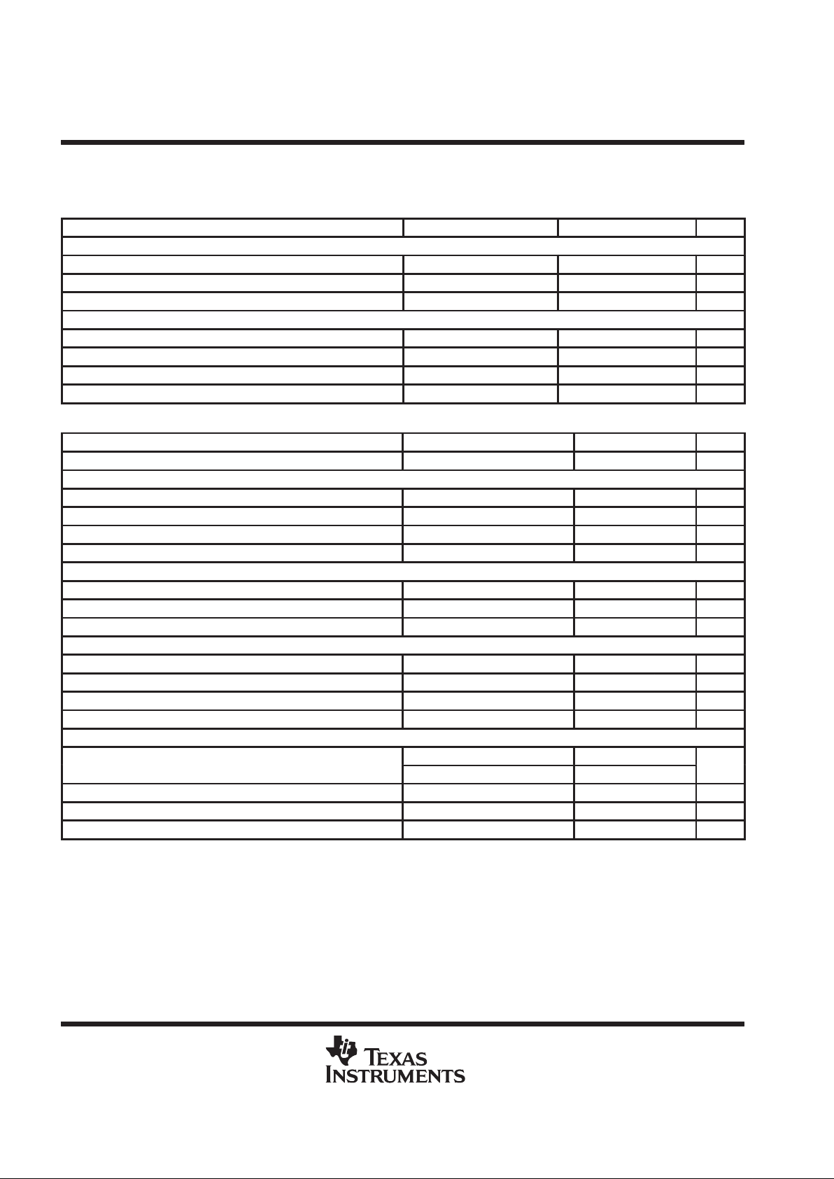
electrical characteristics over recommended operating free-air temperature range, V
CC
= 5 V,
V
REF
= 5 V, f
SCLK
= 20 MHz (unless otherwise noted)
digital specifications
PARAMETER TEST CONDITIONS MIN TYP MAX UNIT
Logic inputs
I
IH
High-level input current VCC = 5 V –50 50 µA
I
IL
Low-level input current VCC = 5 V –50 50 µA
C
i
input capacitance 5 pF
Logic outputs
V
OH
High-level output voltage IOH = 50 µA – 0.5 mA VCC–0.4 V
V
OL
Low-level output voltage IOL = 50 µA – 0.5 mA 0.4 V
I
OZ
High-impedance-state output current –50 50 µA
C
O
Output capacitance 5 pF
dc specifications
PARAMETER TEST CONDITIONS MIN TYP MAX UNIT
Resolution 10 Bits
Accuracy
INL Integral nonlinearity Best fit ±0.5 ±1 LSB
DNL Differential nonlinearity ±0.3 ±1 LSB
Offset error ±0.1 ±0.15 %FSR
Gain error ±0.1 ±0.2 %FSR
Analog input
Input full scale range GND V
CC
V
Input capacitance 15 pF
input leakage current V
AIN
= 0 to V
CC
50 µA
Voltage reference input
V
REF+
Positive reference voltage 3 V
CC
V
V
REF–
Negative reference voltage Internally connects to GND GND V
Input resistance 2 KΩ
Input capcitance 300 pF
Power supply
p
pp
VCC = 5.5 V, f
SCLK
= 20 MHz 5.5 8.5
I
CC
+
I
REF
Operating supply current
VCC = 3 V, f
SCLK
= 10 MHz 2.7
mA
I
PD
Supply current in powerdown mode V
CC
10 µA
Power dissipation VCC = 5 V 25 mW
Power dissipation VCC = 3 V 8 mW

TLV1572
2.7 V TO 5.5 V, 10-BIT, 1.25 MSPS
SERIAL ANALOG-TO-DIGITAL CONVERTER WITH AUTO-POWERDOWN
SLAS171A – DECEMBER 1997– REVISED SEPTEMBER 1998
5
POST OFFICE BOX 655303 • DALLAS, TEXAS 75265
electrical characteristics over recommended operating free-air temperature range, V
CC
= 5 V,
V
REF
= 5 V, f
SCLK
= 20 MHz (unless otherwise noted) (continued)
ac specifications
PARAMETER TEST CONDITIONS MIN TYP MAX UNIT
Signal-to-noise ratio + distortion f
(input)
= 200 kHz 54 58 dB
THD Total harmonic distortion f
(input)
= 200 kHz 56 60 dB
Effective number of bits f
(input)
= 200 kHz 8.7 9.35 Bits
Spurious-free dynamic range f
(input)
= 200 kHz 57 62 dB
Analog Input
BW Full-power bandwidth Source impedance = 1 kΩ 12 MHz
BW Small-signal bandwidth Source impedance = 1 kΩ 20 Mhz
timing specifications
PARAMETER TEST CONDITIONS MIN TYP MAX UNIT
t
c
SCLK period VCC = 4.5 V – 5.5 V 50 ns
t
c
SCLK period VCC = 2.7 V – 3.3 V 100 ns
t
rs
Reset and sampling period 6
SLCK
cycles
t
c
Conversion period 10
SLCK
cycles
t
su1
FS setup time to SCLK falling edge in DSP mode 10 ns
t
h1
FS hold time to SCLK falling edge in DSP mode 4 ns
t
su2
FS setup time to CS falling edge in DSP mode 6 ns
t
h2
FS hold time to CS falling edge in DSP mode 9 ns
t
d1
Output delay after SCLK rising edge in DSP mode 15 25 ns
t
d(L)1
FS falling edge to next SCLK falling edge in DSP mode 6 ns
t
d(L)2
SCLK rising edge after CS falling edge in µC mode 4 ns
t
d2
Output delay after SCLK rising edge in µC mode 15 25 ns
Specifications subject to change without notice.

TLV1572
2.7 V TO 5.5 V, 10-BIT, 1.25 MSPS
SERIAL ANALOG-TO-DIGITAL CONVERTER WITH AUTO-POWERDOWN
SLAS171A – DECEMBER 1997– REVISED SEPTEMBER 1998
6
POST OFFICE BOX 655303 • DALLAS, TEXAS 75265
PARAMETER MEASUREMENT INFORMATION
t
c
1
2
3
t
h1
t
su1
t
su2
t
h2
t
d1
0
t
d(L)1
SCLK
CS
FS
DO
Figure 1. DSP Mode Timing Diagram
1
2
3
00
SCLK
CS
FS
DO
4
0
t
d(L)2
t
d2
Figure 2. µC Mode Timing Diagram

TLV1572
2.7 V TO 5.5 V, 10-BIT, 1.25 MSPS
SERIAL ANALOG-TO-DIGITAL CONVERTER WITH AUTO-POWERDOWN
SLAS171A – DECEMBER 1997– REVISED SEPTEMBER 1998
7
POST OFFICE BOX 655303 • DALLAS, TEXAS 75265
definitions of specifications and terminology
integral nonlinearity
Integral nonlinearity refers to the deviation of each individual code from a line drawn from zero through full scale.
The point used as zero occurs 1/2 LSB before the first code transition. The full scale point is defined as level
1/2 LSB beyond the last code transition. The deviation is measured from the center of each particular code to
the true straight line between these two points.
differential nonlinearity
An ideal ADC exhibits code transitions that are exactly 1 LSB apart. DNL is the deviation from this ideal value.
A differential nonlinearity error of less than ±1 LSB ensures no missing codes.
zero offset
The first code transistion should ideally occur at an analog value 1/2 LSB above V
REF
–. The zero offset error
is defined as the error between the ideal first transistion point and the actual first transistion. This error efectively
shifts left or right an ADC transfer function
gain error
The first code transition should occur at an analog value 1/2 LSB above negative full scale. The last transition
should occur at an analog value 1 1/2 LSB below the nominal full scale. Gain error is the deviation of the actual
difference between first and last code transitions and the ideal difference between first and last code transitions.
signal-to-noise ratio + distortion (SINAD)
SINAD is the ratio of the rms value of the measured input signal to the rms sum of all other spectral components
below the Nyquist frequency, including harmonics but excluding dc. The value for SINAD is expressed in
decibels.
effective number of bits (ENOB)
For a sine wave, SINAD can be expressed in terms of the number of bits. Using the following formula,
N = (SINAD – 1.76)/6.02
it is possible to get a measure of performance expressed as N, the effective number of bits. Thus, effective
number of bits for a device for sine wave inputs at a given input frequency can be calculated directly from its
measured SINAD.
total harmonic distortion (THD)
THD is the ratio of the rms sum of the first six harmonic components to the rms value of the measured input signal
and is expressed as a percentage or in decibels.
spurious free dynamic range (SFDR)
SFDR is the difference in dB between the rms amplitude of the input signal and the largest peak spurious signal.

TLV1572
2.7 V TO 5.5 V, 10-BIT, 1.25 MSPS
SERIAL ANALOG-TO-DIGITAL CONVERTER WITH AUTO-POWERDOWN
SLAS171A – DECEMBER 1997– REVISED SEPTEMBER 1998
8
POST OFFICE BOX 655303 • DALLAS, TEXAS 75265
APPLICATION INFORMATION
The TLV1572 is a 600-ns, 10-bit analog-to-digital converter with the throughput up to 1.25 MSPS at 5 V and
up to 625 KSPS at 3 V respectively. To run at its fastest conversion rate, it must be clocked at 20 MHz at 5 V
or 10 MHz at 3 V. The TLV1572 can be easily interfaced to microcontrollers, ASICs, DSPs, or shift registers.
Its serial interface is designed to be fully compatible with Serial Peripheral Interface (SPI) and TMS320 DSP
serial ports. It requires no hardware to interface between the TL V1572 and the microcontrollers (µCs) with the
SPI serial port or the TMS320 DSPs. However, speed is limited by the SCLK rate of the µC or the DSP.
The TLV1572 interfaces to the DSPs over four lines: CS
, SCLK, DO, and FS, and interfaces to µCs over three
lines: CS
, SCLK, and DO. The FS input should be pulled high in µC mode. The chip is in 3-state and powerdown
mode when CS
is high. After CS falls, the TL V1572 checks the FS input at the CS falling edge to determine the
operation mode. If FS is low, DSP mode is set, else µC mode is set.
interfacing TLV1572 to TMS320 DSPs
The TL V1572 is compatible with Texas Instruments TMS320 DSP serial ports. Figures 3(a) and 3(b) show the
pin connections to interface the TLV1572 to the TMS320 DSPs.
CS
SCLK
FS
DO
XF
CLKX
CLKR
FSX
FSR
DR
TLV1572 TMS320
CS
SCLK
FS
DO
XF
CLKX
CLKR
FSR
DR
TLV1572 TMS320
a) DSP Serial Port Operating in Burst Mode b) FS Externally Generated
From
System
Figure 3. TL V1570 to DSP Interface
1234567 16
0
0 0 0 0 0
LSB
SCLK
CS
FS
DO
MSB
Figure 4. Typical Timing Diagram for DSP Application
In the DSP mode, the FS input should be low when the CS goes low. There is a hold time before the FS input
can go high after the CS
falling edge to ensure proper mode latching. With CS going low, DO comes out of
3-state but the device is still in powerdown until FS (frame sync signal from DSP) goes high.
The TL V1572 checks FS at the falling edges of SCLK. Once FS is detected high, the sampling of input is started.
As soon as FS goes low, the device starts shifting the data out on the DO line. After six null bits, the A/D
conversion data becomes available on the SCLK rising edges and is latched by DSP on the falling edges.
Figure 4 shows the DSP mode timing diagram.

TLV1572
2.7 V TO 5.5 V, 10-BIT, 1.25 MSPS
SERIAL ANALOG-TO-DIGITAL CONVERTER WITH AUTO-POWERDOWN
SLAS171A – DECEMBER 1997– REVISED SEPTEMBER 1998
9
POST OFFICE BOX 655303 • DALLAS, TEXAS 75265
APPLICATION INFORMATION
interfacing TLV1572 to TMS320 DSPs (continued)
The TL V1572 goes into auto-powerdown after the LSB is shifted out. The next FS pulls it out of auto-powerdown
as shown in Figure 5. If FS comes on the 16th bit, the next conversion cycle starts from the next rising edge
of SCLK allowing back to back conversions as shown in Figure 6. An FS high in the middle of a conversion cycle
resets the device and starts a new conversion cycle. Therefore variable-bit transfer is supported if FS appears
earlier.
CS
can be pulled high asynchronously to put the device into 3-state and powerdown. CS can also be pulled low
asynchronously to start checking for FS on the falling edges of the clock.
1234567 16
0
0000
0
LSB(N)
SCLK
CS
FS
DO
MSB
1234567 16
00000
0
LSB(N+1)
MSB(N+1)
Auto-Powerdown
Sampling Conversion
Sample (N) Sample (N+1)
(N)
6 Leading Zeros
Figure 5. DSP Application Timing (Intermittent Conversion)
1234567 16
0
00
0
00
SCLK
CS
FS
DO
MSB
1234567 16
00000
0
0
LSB(N)
LSB(N+1)
Sampling Conversion
Sample (N) Sample (N+1)
(N)
6 Leading
Zeros
MSB(N+1)
Figure 6. DSP Application Timing (Continuous Conversion)
key points
1. When CS
goes low, if FS is low, it is in DSP mode. FS is sampled twice by a CS falling edge and again by
an internally delayed CS
falling edge. Even if a glitch appears and one latch latches 1 and another latches
0, the device goes into DSP mode (µC mode requires both latches to latch 1). There is a hold time before
FS can go high again after the CS
falling edge to ensure proper mode latching as detailed above. With CS
going low, DO is in 3-state and the device is in powerdown until a FS rising edge.
2. The TLV1572 checks for FS at every falling edge of SCLK. If FS is detected high, the device goes into reset.
When FS goes low, the TLV1572 waits for the DSP to latch the first 0 bit.
3. Sampling occurs from first falling edge of SCLK after FS going low until the rising edge when the 6th 0 bit
is sent out. Thereafter decisions are taken on the rising edges and data is sent out on the rising edges (1
bit delayed). The DSP samples on the falling edge of SCLK. Data is padded with 6 leading zeros.

TLV1572
2.7 V TO 5.5 V, 10-BIT, 1.25 MSPS
SERIAL ANALOG-TO-DIGITAL CONVERTER WITH AUTO-POWERDOWN
SLAS171A – DECEMBER 1997– REVISED SEPTEMBER 1998
10
POST OFFICE BOX 655303 • DALLAS, TEXAS 75265
APPLICATION INFORMATION
key points (continued)123
4. Note that the device goes into autopowerdown on the 17th falling edge of SCLK (just after the LSB). The
FS rising edge pulls it out of autopowerdown. If FS comes on the 16th bit, the next conversion cycle starts
from the next rising edge allowing back to back conversions. An FS in the middle of a conversion cycle starts
a new conversion cycle. Thus variable-bit transfer is supported if FS appears earlier.
5. DO goes into 3-state on the 17th rising edge and comes out on a FS rising edge.
6. CS
can be pulled high asynchronously to put the device into 3-state and powerdown. CS may also be pulled
low asynchronously to start checking for FS on the falling edges of the clock.
For applications where the analog input must be sampled at a precise instant in time, data conversion can be
initiated by an external conversion start pulse which is completely asynchronous to the SCLK as shown in Figure
4. When a conversion start pulse is received, the pulse is used as a frame sync (FS) signal to initiate the data
conversion and transfer. The corresponding timing diagram is shown in Figure 6.
interfacing TLV1572 to SPI/QSPI compatible microcontrollers (µCs)
The TLV1572 is compatible with SPI and QSPI serial interface standards (Note: the TLV1572 supports the
following SPI clock options: clock_polarity= 0, i.e. SCLK idles low, and clock_phase = 1). Figure 7 shows the
pin connections to interface the TLV1572 to SPI/QSPI compatible microcontrollers.
CS
SCLK
FS
DO
XF
SCLK
DR
TLV1572 µC
V
CC
Figure 7. TLV1572 to µC Interface
1 2 345 67 16
0 0 0
0
0
0MSB
SCLK
CS
FS
SDOUT
LSB
Figure 8. Typical Timing Diagram for µC Application
To use the TLV1572 in a non-DSP application, the FS input should be pulled high as shown in Figure 8.
A total of 16 clocks are normally supplied for each conversion. If the µC cannot take in 16 bits at a time, it may
take 8 bits with 8 clocks and next 8 bits with another 8 clocks. CS
should be kept low throughout the conversion.
The delay between these two 8-clock periods should not be longer than 100 µs.

TLV1572
2.7 V TO 5.5 V, 10-BIT, 1.25 MSPS
SERIAL ANALOG-TO-DIGITAL CONVERTER WITH AUTO-POWERDOWN
SLAS171A – DECEMBER 1997– REVISED SEPTEMBER 1998
11
POST OFFICE BOX 655303 • DALLAS, TEXAS 75265
APPLICATION INFORMATION
interfacing TLV1572 to SPI/QSPI compatible microcontrollers(µCs) (continued)
Unlike the DSP mode in which the conversion is initiated by the FS input signal from the DSP, the conversion
is initiated by the incoming SCLK after CS
falls. Sampling of the input is started on the first rising edge of SCLK
after CS
goes low. After six null bits, the A/D conversion data becomes available on SCLK rising edges and is
latched by the µC on the falling edges. CS
can be pulled high during the conversion before the LSB is shifted
out to use the device as a lower resolution ADC. Figure 9 shows the µC mode timing diagram.
The device goes into autopowerdown after the LSB is shifted out and is brought out of powerdown by the next
clock rising edge as shown in Figure 9.
12 34 5 6 7 16
0
0 0
0
0 0
LSB (N)
SCLK
CS
FS
DO
MSB
1234567 16
0 0 00
0
Auto-Powerdown
0
LSB(N+1)
Sampling Conversion
Sample (N)
(N)
MSB(N+1)
Figure 9. µC Application Timing Diagram
key points
1. When CS
goes low, if FS is high, it is in µ C ({Q}SPI) mode. Thus, FS should be tied to VDD. FS is latched
twice, on the falling edge of CS
and again on an internally delayed falling edge of CS. Only if both latches
latch 1, then µC mode is set else DSP mode is set. Only polarity = 0 is supported, i.e. SCLK idles low. Only
clock_phase = 1 is supported as shown in the timing diagrams.
2. For each conversion 16 clocks have to be supplied. If the µC cannot take in 16 bits at a time, it may take
8 bits with 8 clocks and the next 8 bits with another 8 clocks keeping CS
low throughout the conversion.
The delay between these two 8-clock periods should not be longer than 100 µs.
3. Sampling starts on the first rising edge of SCLK and ends on the edge when the 6th 0 bit is sent out.
Decisions are made on the rising edge and data is output on the same edge but a bit delayed to avoid noise.
4. The device goes into autopowerdown on the falling edge of the 16th clock and is brought out of powerdown
by next first (17th) clock rising edge.
5. If the (Q)SPI wants less than a 16-bit transfer, CS
must go high after each transfer. The falling edge of CS
resets the TL V1572 for the next conversion. Thus a 14-bit transfer is possible when using the device as an
8-bit A/D.
6. CS
going high puts the device in 3-state and complete powerdown. CS going low sets the mode and pulls
DO out of 3-state.

TLV1572
2.7 V TO 5.5 V, 10-BIT, 1.25 MSPS
SERIAL ANALOG-TO-DIGITAL CONVERTER WITH AUTO-POWERDOWN
SLAS171A – DECEMBER 1997– REVISED SEPTEMBER 1998
12
POST OFFICE BOX 655303 • DALLAS, TEXAS 75265
MECHANICAL INFORMATION
D (R-PDSO-G**) PLASTIC SMALL-OUTLINE PACKAGE
14 PIN SHOWN
4040047/D 10/96
0.228 (5,80)
0.244 (6,20)
0.069 (1,75) MAX
0.010 (0,25)
0.004 (0,10)
1
14
0.014 (0,35)
0.020 (0,51)
A
0.157 (4,00)
0.150 (3,81)
7
8
0.044 (1,12)
0.016 (0,40)
Seating Plane
0.010 (0,25)
PINS **
0.008 (0,20) NOM
A MIN
A MAX
DIM
Gage Plane
0.189
(4,80)
(5,00)
0.197
8
(8,55)
(8,75)
0.337
14
0.344
(9,80)
16
0.394
(10,00)
0.386
0.004 (0,10)
M
0.010 (0,25)
0.050 (1,27)
0°–8°
NOTES: A. All linear dimensions are in inches (millimeters).
B. This drawing is subject to change without notice.
C. Body dimensions do not include mold flash or protrusion, not to exceed 0.006 (0,15).
D. Falls within JEDEC MS-012

IMPORTANT NOTICE
T exas Instruments and its subsidiaries (TI) reserve the right to make changes to their products or to discontinue
any product or service without notice, and advise customers to obtain the latest version of relevant information
to verify, before placing orders, that information being relied on is current and complete. All products are sold
subject to the terms and conditions of sale supplied at the time of order acknowledgement, including those
pertaining to warranty, patent infringement, and limitation of liability.
TI warrants performance of its semiconductor products to the specifications applicable at the time of sale in
accordance with TI’s standard warranty. Testing and other quality control techniques are utilized to the extent
TI deems necessary to support this warranty. Specific testing of all parameters of each device is not necessarily
performed, except those mandated by government requirements.
CERT AIN APPLICATIONS USING SEMICONDUCTOR PRODUCTS MAY INVOLVE POTENTIAL RISKS OF
DEATH, PERSONAL INJURY, OR SEVERE PROPERTY OR ENVIRONMENTAL DAMAGE (“CRITICAL
APPLICATIONS”). TI SEMICONDUCTOR PRODUCTS ARE NOT DESIGNED, AUTHORIZED, OR
WARRANTED TO BE SUITABLE FOR USE IN LIFE-SUPPORT DEVICES OR SYSTEMS OR OTHER
CRITICAL APPLICATIONS. INCLUSION OF TI PRODUCTS IN SUCH APPLICA TIONS IS UNDERST OOD TO
BE FULLY AT THE CUSTOMER’S RISK.
In order to minimize risks associated with the customer’s applications, adequate design and operating
safeguards must be provided by the customer to minimize inherent or procedural hazards.
TI assumes no liability for applications assistance or customer product design. TI does not warrant or represent
that any license, either express or implied, is granted under any patent right, copyright, mask work right, or other
intellectual property right of TI covering or relating to any combination, machine, or process in which such
semiconductor products or services might be or are used. TI’s publication of information regarding any third
party’s products or services does not constitute TI’s approval, warranty or endorsement thereof.
Copyright 1998, Texas Instruments Incorporated
 Loading...