

Texas Instruments TLC320AC01CPMR, TLC320AC01CPM, TLC320AC01CFN, TLC320AC01CFNR, TLC320AC01CDW Datasheet

TLC320AC01C
Data Manual
Single-Supply Analog Interface Circuit
SLAS057D
October 1996
Printed on Recycled Paper

IMPORTANT NOTICE
T exas Instruments (TI) reserves the right to make changes to its products or to discontinue any
semiconductor product or service without notice, and advises its customers to obtain the latest
version of relevant information to verify, before placing orders, that the information being relied
on is current.
TI warrants performance of its semiconductor products and related software to the specifications
applicable at the time of sale in accordance with TI’s standard warranty . T esting and other quality
control techniques are utilized to the extent TI deems necessary to support this warranty.
Specific testing of all parameters of each device is not necessarily performed, except those
mandated by government requirements.
Certain applications using semiconductor products may involve potential risks of death,
personal injury, or severe property or environmental damage (“Critical Applications”).
TI SEMICONDUCTOR PRODUCTS ARE NOT DESIGNED, INTENDED, AUTHORIZED, OR
WARRANTED TO BE SUITABLE FOR USE IN LIFE-SUPPORT APPLICATIONS, DEVICES
OR SYSTEMS OR OTHER CRITICAL APPLICATIONS.
Inclusion of TI products in such applications is understood to be fully at the risk of the customer.
Use of TI products in such applications requires the written approval of an appropriate TI officer.
Questions concerning potential risk applications should be directed to TI through a local SC
sales office.
In order to minimize risks associated with the customer’s applications, adequate design and
operating safeguards should be provided by the customer to minimize inherent or procedural
hazards.
TI assumes no liability for applications assistance, customer product design, software
performance, or infringement of patents or services described herein. Nor does TI warrant or
represent that any license, either express or implied, is granted under any patent right, copyright,
mask work right, or other intellectual property right of TI covering or relating to any combination,
machine, or process in which such semiconductor products or services might be or are used.
Copyright 1996, Texas Instruments Incorporated

iii
Contents
Section Title Page
1 Introduction 1–1. . . . . . . . . . . . . . . . . . . . . . . . . . . . . . . . . . . . . . . . . . . . . . . . . . . . . . . . . . . . .
1.1 Features 1–2. . . . . . . . . . . . . . . . . . . . . . . . . . . . . . . . . . . . . . . . . . . . . . . . . . . . . . . . . . . .
1.2 Functional Block Diagram 1–3. . . . . . . . . . . . . . . . . . . . . . . . . . . . . . . . . . . . . . . . . . . . .
1.3 Terminal Assignments 1–3. . . . . . . . . . . . . . . . . . . . . . . . . . . . . . . . . . . . . . . . . . . . . . . .
1.4 Terminal Functions 1–5. . . . . . . . . . . . . . . . . . . . . . . . . . . . . . . . . . . . . . . . . . . . . . . . . . .
1.5 Register Functional Summary 1–8. . . . . . . . . . . . . . . . . . . . . . . . . . . . . . . . . . . . . . . . .
2 Detailed Description 2–1. . . . . . . . . . . . . . . . . . . . . . . . . . . . . . . . . . . . . . . . . . . . . . . . . . . . .
2.1 Definitions and Terminology 2–1. . . . . . . . . . . . . . . . . . . . . . . . . . . . . . . . . . . . . . . . . . .
2.2 Reset and Power-Down Functions 2–2. . . . . . . . . . . . . . . . . . . . . . . . . . . . . . . . . . . . .
2.2.1 Reset 2–2. . . . . . . . . . . . . . . . . . . . . . . . . . . . . . . . . . . . . . . . . . . . . . . . . . . . . . . .
2.2.2 Conditions of Reset 2–2. . . . . . . . . . . . . . . . . . . . . . . . . . . . . . . . . . . . . . . . . . . .
2.2.3 Software and Hardware Power-Down 2–2. . . . . . . . . . . . . . . . . . . . . . . . . . . . .
2.2.4 Register Default Values After POR,
Software Reset, or RESET
Is Applied 2–2. . . . . . . . . . . . . . . . . . . . . . . . . . . .
2.3 Master-Slave Terminal Function 2–4. . . . . . . . . . . . . . . . . . . . . . . . . . . . . . . . . . . . . . .
2.4 ADC Signal Channel 2–4. . . . . . . . . . . . . . . . . . . . . . . . . . . . . . . . . . . . . . . . . . . . . . . . .
2.5 DAC Signal Channel 2–4. . . . . . . . . . . . . . . . . . . . . . . . . . . . . . . . . . . . . . . . . . . . . . . . .
2.6 Serial Interface 2–4. . . . . . . . . . . . . . . . . . . . . . . . . . . . . . . . . . . . . . . . . . . . . . . . . . . . . .
2.7 Number of Slaves 2–5. . . . . . . . . . . . . . . . . . . . . . . . . . . . . . . . . . . . . . . . . . . . . . . . . . . .
2.8 Required Minimum Number of MCLK Periods 2–6. . . . . . . . . . . . . . . . . . . . . . . . . . .
2.8.1 TLC320AC01 AIC Master-Slave Summary 2–6. . . . . . . . . . . . . . . . . . . . . . . .
2.8.2 Notes on TLC320AC01/02 AIC Master-Slave Operation 2–7. . . . . . . . . . . . .
2.9 Operating Frequencies 2–9. . . . . . . . . . . . . . . . . . . . . . . . . . . . . . . . . . . . . . . . . . . . . . .
2.9.1 Master and Stand-Alone Operating Frequencies 2–9. . . . . . . . . . . . . . . . . . .
2.9.2 Slave and Codec Operating Frequencies 2–9. . . . . . . . . . . . . . . . . . . . . . . . .
2.10 Switched-Capacitor Filter Frequency (FCLK) 2–9. . . . . . . . . . . . . . . . . . . . . . . . . . . .
2.1 1 Filter Bandwidths 2–9. . . . . . . . . . . . . . . . . . . . . . . . . . . . . . . . . . . . . . . . . . . . . . . . . . . .
2.12 Master and Stand-Alone Modes 2–9. . . . . . . . . . . . . . . . . . . . . . . . . . . . . . . . . . . . . . .
2.12.1 Register Programming 2–9. . . . . . . . . . . . . . . . . . . . . . . . . . . . . . . . . . . . . . . . . .
2.12.2 Master and Stand-Alone Functional Sequence 2–10. . . . . . . . . . . . . . . . . . . . .
2.13 Slave and Codec Modes 2–10. . . . . . . . . . . . . . . . . . . . . . . . . . . . . . . . . . . . . . . . . . . . . .
2.13.1 Slave and Codec Functional Sequence 2–11. . . . . . . . . . . . . . . . . . . . . . . . . . .
2.13.2 Slave Register Programming 2–11. . . . . . . . . . . . . . . . . . . . . . . . . . . . . . . . . . . .
2.14 Terminal Functions 2–11. . . . . . . . . . . . . . . . . . . . . . . . . . . . . . . . . . . . . . . . . . . . . . . . . . .
2.14.1 Frame-Sync Function 2–11. . . . . . . . . . . . . . . . . . . . . . . . . . . . . . . . . . . . . . . . . .
2.14.2 Data Out (DOUT) 2–12. . . . . . . . . . . . . . . . . . . . . . . . . . . . . . . . . . . . . . . . . . . . . .
2.14.3 Data In (DIN) 2–12. . . . . . . . . . . . . . . . . . . . . . . . . . . . . . . . . . . . . . . . . . . . . . . . . .
2.14.4 Hardware Program Terminals (FC1 and FC0) 2–12. . . . . . . . . . . . . . . . . . . . . .
2.14.5 Midpoint Voltages (ADC V
MID
and DAC V
MID
) 2–13. . . . . . . . . . . . . . . . . . . . .
2.15 Device Functions 2–13. . . . . . . . . . . . . . . . . . . . . . . . . . . . . . . . . . . . . . . . . . . . . . . . . . . .
2.15.1 Phase Adjustment 2–13. . . . . . . . . . . . . . . . . . . . . . . . . . . . . . . . . . . . . . . . . . . . .
2.15.2 Analog Loopback 2–14. . . . . . . . . . . . . . . . . . . . . . . . . . . . . . . . . . . . . . . . . . . . . .

iv
Contents (Continued)
Section Title Page
2.15.3 16-Bit Mode 2–14. . . . . . . . . . . . . . . . . . . . . . . . . . . . . . . . . . . . . . . . . . . . . . . . . . .
2.15.4 Free-Run Mode 2–14. . . . . . . . . . . . . . . . . . . . . . . . . . . . . . . . . . . . . . . . . . . . . . . .
2.15.5 Force Secondary Communication 2–14. . . . . . . . . . . . . . . . . . . . . . . . . . . . . . . .
2.15.6 Enable Analog Input Summing 2–15. . . . . . . . . . . . . . . . . . . . . . . . . . . . . . . . . . .
2.15.7 DAC Channel (sin x)/x Error Correction 2–15. . . . . . . . . . . . . . . . . . . . . . . . . . .
2.16 Serial Communications 2–15. . . . . . . . . . . . . . . . . . . . . . . . . . . . . . . . . . . . . . . . . . . . . . .
2.16.1 Stand-Alone and Master-Mode Word Sequence and
Information Content During Primary and
Secondary Communications 2–15. . . . . . . . . . . . . . . . . . . . . . . . . . . . . . . . . . . . .
2.16.2 Slave and Codec-Mode Word Sequence and
Information Content During Primary and
Secondary Communications 2–16. . . . . . . . . . . . . . . . . . . . . . . . . . . . . . . . . . . . .
2.17 Request for Secondary Serial Communication and Phase Shift 2–17. . . . . . . . . . . .
2.17.1 Initiating a Request 2–17. . . . . . . . . . . . . . . . . . . . . . . . . . . . . . . . . . . . . . . . . . . .
2.17.2 Normal Combinations of Control 2–17. . . . . . . . . . . . . . . . . . . . . . . . . . . . . . . . .
2.17.3 Additional Control Options 2–17. . . . . . . . . . . . . . . . . . . . . . . . . . . . . . . . . . . . . .
2.18 Primary Serial Communications 2–18. . . . . . . . . . . . . . . . . . . . . . . . . . . . . . . . . . . . . . . .
2.18.1 Primary Serial Communications Data Format 2–19. . . . . . . . . . . . . . . . . . . . . .
2.18.2 Data Format From DOUT During
Primary Serial Communications 2–19. . . . . . . . . . . . . . . . . . . . . . . . . . . . . . . . . .
2.19 Secondary Serial Communications 2–19. . . . . . . . . . . . . . . . . . . . . . . . . . . . . . . . . . . . .
2.19.1 Data Format to DIN During Secondary Serial Communications 2–19. . . . . . .
2.19.2 Control Data-Bit Function in Secondary Serial Communication 2–19. . . . . . .
2.20 Internal Register Format 2–20. . . . . . . . . . . . . . . . . . . . . . . . . . . . . . . . . . . . . . . . . . . . . .
2.20.1 Pseudo-Register 0 (No-Op Address) 2–20. . . . . . . . . . . . . . . . . . . . . . . . . . . . .
2.20.2 Register 1 (A Register) 2–20. . . . . . . . . . . . . . . . . . . . . . . . . . . . . . . . . . . . . . . . .
2.20.3 Register 2 (B Register) 2–21. . . . . . . . . . . . . . . . . . . . . . . . . . . . . . . . . . . . . . . . .
2.20.4 Register 3 (A′ Register) 2–21. . . . . . . . . . . . . . . . . . . . . . . . . . . . . . . . . . . . . . . . .
2.20.5 Register 4 (Amplifier Gain-Select Register) 2–22. . . . . . . . . . . . . . . . . . . . . . . .
2.20.6 Register 5 (Analog Configuration Register) 2–22. . . . . . . . . . . . . . . . . . . . . . . .
2.20.7 Register 6 (Digital Configuration Register) 2–23. . . . . . . . . . . . . . . . . . . . . . . . .
2.20.8 Register 7 (Frame-Sync Delay Register) 2–23. . . . . . . . . . . . . . . . . . . . . . . . . .
2.20.9 Register 8 (Frame-Sync Number Register) 2–24. . . . . . . . . . . . . . . . . . . . . . . .
3 Specifications 3–1. . . . . . . . . . . . . . . . . . . . . . . . . . . . . . . . . . . . . . . . . . . . . . . . . . . . . . . . . . .
3.1 Absolute Maximum Ratings Over Operating
Free-Air Temperature Range 3–1. . . . . . . . . . . . . . . . . . . . . . . . . . . . . . . . . . . . . . . . . .
3.2 Recommended Operating Conditions 3–1. . . . . . . . . . . . . . . . . . . . . . . . . . . . . . . . . . .
3.3 Electrical Characteristics Over Recommended Range of Operating
Free-Air Temperature, MCLK = 5.184 MHz, V
DD
= 5 V, Outputs
Unloaded, Total Device 3–2. . . . . . . . . . . . . . . . . . . . . . . . . . . . . . . . . . . . . . . . . . . . . . .
3.4 Electrical Characteristics Over Recommended Range of Operating
Free-Air Temperature, V
DD
= 5 V, Digital I/O Terminals (DIN, DOUT, EOC,
FC0, FC1, FS
, FSD, MCLK, M/S, SCLK) 3–2. . . . . . . . . . . . . . . . . . . . . . . . . . . . . . . .

v
Contents (Continued)
Section Title Page
3.5 Electrical Characteristics Over Recommended Range of Operating
Free-Air Temperature, V
DD
= 5 V, ADC and DAC Channels 3–2. . . . . . . . . . . . . . .
3.5.1 ADC Channel Filter Transfer Function,
FCLK = 144 kHz, f
s
= 8 kHz 3–2. . . . . . . . . . . . . . . . . . . . . . . . . . . . . . . . . . . . .
3.5.2 ADC Channel Input, V
DD
= 5 V,
Input Amplifier Gain = 0 dB 3–3. . . . . . . . . . . . . . . . . . . . . . . . . . . . . . . . . . . . . .
3.5.3 ADC Channel Signal-to-Distortion Ratio,
V
DD
= 5 V, fs = 8 kHz 3–3. . . . . . . . . . . . . . . . . . . . . . . . . . . . . . . . . . . . . . . . . . .
3.5.4 DAC Channel Filter Transfer Function,
FCLK = 144 kHz, f
s
= 9.6 kHz, VDD = 5 V 3–3. . . . . . . . . . . . . . . . . . . . . . . . .
3.5.5 DAC Channel Signal-to-Distortion Ratio,
V
DD
= 5 V, fs = 8 kHz 3–4. . . . . . . . . . . . . . . . . . . . . . . . . . . . . . . . . . . . . . . . . . .
3.5.6 System Distortion, V
DD
= 5 V, fs = 8 kHz,
FCLK = 144 kHz 3–4. . . . . . . . . . . . . . . . . . . . . . . . . . . . . . . . . . . . . . . . . . . . . . .
3.5.7 Noise, Low-Pass and Band-Pass Switched-
Capacitor Filters Included, V
DD
= 5 V 3–5. . . . . . . . . . . . . . . . . . . . . . . . . . . . .
3.5.8 Absolute Gain Error, V
DD
= 5 V, fs = 8 kHz 3–5. . . . . . . . . . . . . . . . . . . . . . .
3.5.9 Relative Gain and Dynamic Range, V
DD
= 5 V, fs = 8 kHz 3–5. . . . . . . . . . .
3.5.10 Power-Supply Rejection, V
DD
= 5 V 3–6. . . . . . . . . . . . . . . . . . . . . . . . . . . . . .
3.5.11 Crosstalk Attenuation, V
DD
= 5 V 3–6. . . . . . . . . . . . . . . . . . . . . . . . . . . . . . . .
3.5.12 Monitor Output Characteristics, V
DD
= 5 V 3–7. . . . . . . . . . . . . . . . . . . . . . . .
3.6 Timing Requirements and Specifications in Master Mode 3–8. . . . . . . . . . . . . . . . .
3.6.1 Recommended Input Timing Requirements for
Master Mode, V
DD
= 5 V 3–8. . . . . . . . . . . . . . . . . . . . . . . . . . . . . . . . . . . . . . . .
3.6.2 Operating Characteristics Over Recommended Range of
Operating Free-Air Temperature, V
DD
= 5 V 3–8. . . . . . . . . . . . . . . . . . . . . . .
3.7 Timing Requirements and Specifications in Slave Mode and
Codec Emulation Mode 3–9. . . . . . . . . . . . . . . . . . . . . . . . . . . . . . . . . . . . . . . . . . . . . . .
3.7.1 Recommended Input Timing Requirements for
Slave Mode, V
DD
= 5 V 3–9. . . . . . . . . . . . . . . . . . . . . . . . . . . . . . . . . . . . . . . . .
3.7.2 Operating Characteristics Over Recommended Range of Operating
Free-Air Temperature, V
DD
= 5 V 3–9. . . . . . . . . . . . . . . . . . . . . . . . . . . . . . . .
4 Parameter Measurement Information 4–1. . . . . . . . . . . . . . . . . . . . . . . . . . . . . . . . . . . . . .
5 T ypical Characteristics 5–1. . . . . . . . . . . . . . . . . . . . . . . . . . . . . . . . . . . . . . . . . . . . . . . . . . .
6 Application Information 6–1. . . . . . . . . . . . . . . . . . . . . . . . . . . . . . . . . . . . . . . . . . . . . . . . . .
Appendix A Primary Control Bits A–1. . . . . . . . . . . . . . . . . . . . . . . . . . . . . . . . . . . . . . . . . .
Appendix B Secondary Communications B–1. . . . . . . . . . . . . . . . . . . . . . . . . . . . . . . . . . .
Appendix C TLC320AC01C/TLC320AC02C Specification Comparisons C–1. . . . . . .
Appendix D Multiple TLC320AC01/TLC320AC02 Analog Interface Circuits
on One TMS320C5X DSP Serial Port D–1. . . . . . . . . . . . . . . . . . . . . . . . . . .
Appendix E Mechanical Data E–1. . . . . . . . . . . . . . . . . . . . . . . . . . . . . . . . . . . . . . . . . . . . . .

vi
List of Illustrations
Figure Title Page
1–1 Control Flow Diagram 1–7. . . . . . . . . . . . . . . . . . . . . . . . . . . . . . . . . . . . . . . . . . . . . . . . .
2–1 Functional Sequence for Primary and Secondary Communication 2–5. . . . . . . . . . .
2–2 Timing Sequence 2–6. . . . . . . . . . . . . . . . . . . . . . . . . . . . . . . . . . . . . . . . . . . . . . . . . . . . .
2–3 Master and Stand-Alone Functional Sequence 2–16. . . . . . . . . . . . . . . . . . . . . . . . . . . .
2–4 Slave and Codec Functional Sequence 2–16. . . . . . . . . . . . . . . . . . . . . . . . . . . . . . . . . .
4–1 IN+ and IN– Gain-Control Circuitry 4–1. . . . . . . . . . . . . . . . . . . . . . . . . . . . . . . . . . . . . .
4–2 AIC Stand-Alone and Master-Mode Timing 4–2. . . . . . . . . . . . . . . . . . . . . . . . . . . . . . .
4–3 AIC Slave and Codec Emulation Mode 4–2. . . . . . . . . . . . . . . . . . . . . . . . . . . . . . . . . . .
4–4 Master or Stand-Alone FS
and FSD Timing 4–3. . . . . . . . . . . . . . . . . . . . . . . . . . . . . . .
4–5 Slave FS
to FSD Timing 4–3. . . . . . . . . . . . . . . . . . . . . . . . . . . . . . . . . . . . . . . . . . . . . . .
4–6 Slave SCLK to FSD
Timing 4–3. . . . . . . . . . . . . . . . . . . . . . . . . . . . . . . . . . . . . . . . . . . . .
4–7 DOUT Enable Timing From Hi-Z 4–4. . . . . . . . . . . . . . . . . . . . . . . . . . . . . . . . . . . . . . . .
4–8 DOUT Delay Timing to Hi-Z 4–4. . . . . . . . . . . . . . . . . . . . . . . . . . . . . . . . . . . . . . . . . . . .
4–9 EOC Frame Timing 4–4. . . . . . . . . . . . . . . . . . . . . . . . . . . . . . . . . . . . . . . . . . . . . . . . . . . .
4–10 Master-Slave Frame-Sync Timing After a Delay Has Been
Programmed Into the FSD Registers 4–5. . . . . . . . . . . . . . . . . . . . . . . . . . . . . . . . . . . .
4–11 Master and Slave Frame-Sync Sequence with One Slave 4–5. . . . . . . . . . . . . . . . . .
6–1 Stand-Alone Mode (to DSP Interface) 6–1. . . . . . . . . . . . . . . . . . . . . . . . . . . . . . . . . . . .
6–2 Codec Mode (to DSP Interface) 6–1. . . . . . . . . . . . . . . . . . . . . . . . . . . . . . . . . . . . . . . . .
6–3 Master With Slave (to DSP Interface) 6–2. . . . . . . . . . . . . . . . . . . . . . . . . . . . . . . . . . . .
6–4 Single-Ended Input (Ground Referenced) 6–2. . . . . . . . . . . . . . . . . . . . . . . . . . . . . . . .
6–5 Single-Ended to Differential Input (Ground Referenced) 6–3. . . . . . . . . . . . . . . . . . . .
6–6 Differential Load 6–3. . . . . . . . . . . . . . . . . . . . . . . . . . . . . . . . . . . . . . . . . . . . . . . . . . . . . .
6–7 Differential Output Drive (Ground Referenced) 6–3. . . . . . . . . . . . . . . . . . . . . . . . . . . .
6–8 Low-Impedance Output Drive 6–4. . . . . . . . . . . . . . . . . . . . . . . . . . . . . . . . . . . . . . . . . . .
6–9 Single-Ended Output Drive (Ground Referenced) 6–4. . . . . . . . . . . . . . . . . . . . . . . . .
List of Tables
Table Title Page
1–1 Operating Frequencies 1–7. . . . . . . . . . . . . . . . . . . . . . . . . . . . . . . . . . . . . . . . . . . . . . . .
2–1 Master-Slave Selection 2–4. . . . . . . . . . . . . . . . . . . . . . . . . . . . . . . . . . . . . . . . . . . . . . . .
2–2 Sampling Variation With A′ 2–13. . . . . . . . . . . . . . . . . . . . . . . . . . . . . . . . . . . . . . . . . . . . .
2–3 Software and Hardware Requests for Secondary Serial-Communication and
Phase-Shift Truth Table 2–18. . . . . . . . . . . . . . . . . . . . . . . . . . . . . . . . . . . . . . . . . . . . . . . .
4–1 Gain Control (Analog Input Signal Required for
Full-Scale Bipolar A/D-Conversion 2s Complement) 4–1. . . . . . . . . . . . . . . . . . . . . . .

1–1
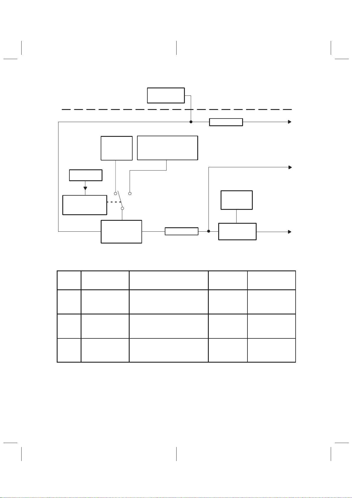
1 Introduction
The TLC320AC01† analog interface circuit (AIC) is an audio-band processor that provides an
analog-to-digital and digital-to-analog input/output interface system on a single monolithic CMOS chip. This
device integrates a band-pass switched-capacitor antialiasing input filter, a 14-bit-resolution
analog-to-digital converter (ADC), a 14-bit-resolution digital-to-analog converter (DAC), a low-pass
switched-capacitor output-reconstruction filter, (sin x)/x compensation, and a serial port for data and control
transfers.
The internal circuit configuration and performance parameters are determined by reading control
information into the eight available data registers. The register data sets up the device for a given mode of
operation and application.
The major functions of the TLC320AC01 are:
1. To convert audio-signal data to digital format by the ADC channel
2. To provide the interface and control logic to transfer data between its serial input and output
terminals and a digital signal processor (DSP) or microprocessor
3. To convert received digital data back to an audio signal through the DAC channel
The antialiasing input low-pass filter is a switched-capacitor filter with a sixth-order elliptic characteristic. The
high-pass filter is a single-pole filter to preserve low-frequency response as the low-pass filter cutoff is
adjusted. There is a three-pole continuous-time filter that precedes this filter to eliminate any aliasing caused
by the filter clock signal.
The output-reconstruction switched-capacitor filter is a sixth-order elliptic transitional low-pass filter followed
by a second-order (sin x)/x correction filter. This filter is followed by a three-pole continuous-time filter to
eliminate images of the filter clock signal.
The TLC320AC01 consists of two signal-processing channels, an ADC channel and a DAC channel, and
the associated digital control. The two channels operate synchronously; data reception at the DAC channel
and data transmission from the ADC channel occur during the same time interval. The data transfer is in
2s-complement format.
There are three basic modes of operation available: the stand-alone analog-interface mode, the
master-slave mode, and the linear-codec mode. In the stand-alone mode, the TLC320AC01 generates the
shift clock and frame synchronization for the data transfers and is the only AIC used. The master-slave mode
has one TLC320AC01 as the master that generates the master-shift clock and frame synchronization; the
remaining AICs are slaves to these signals. In the linear-codec mode, the shift clock and the framesynchronization signals are externally generated and the timing can be any of the standard codec-timing
patterns.
Typical applications for this device include modems, speech processing, analog interface for DSPs,
industrial-process control, acoustical-signal processing, spectral analysis, data acquisition, and
instrumentation recorders.
The TLC320AC01C is characterized for operation from 0°C to 70°C.
†
The TLC320AC01 is functionally equivalent to the TLC320AC02 and differs in the electrical specifications as shown
in Appendix C.

1–2
1.1 Features
• General-Purpose Signal-Processing Analog Front End (AFE)
• Single 5-V Power Supply
• Power Dissipation . . . 100 mW Typ
• Signal-to-Distortion Ratio . . . 70 dB Typ
• Programmable Filter Bandwidths (Up to 10.8 kHz) and Synchronous ADC and DAC Sampling
• Serial-Port Interface
• Monitor Output With Programmable Gains of 0 dB, –8 dB, –18 dB, and Squelch
• Two Sets of Differential Inputs With Programmable Gains of 0 dB, 6 dB, 12 dB, and Squelch
• Differential or Single-Ended Analog Output With Programmable Gains of 0 dB, –6 dB, –12 dB,
and Squelch
• Differential Outputs Drive 3-V Peak Into a 600-
Ω Differential Load
• Differential Architecture Throughout
• 1-
µm Advanced LinEPIC Process
• 14-Bit Dynamic-Range ADC and DAC
• 2s-Complement Data Format
• Application Report Available
†
†
Designing with the TLC320AC01 Analog Interface for DSPs (SLAA006)
LinEPIC is a trademark of Texas Instruments Incorporated.
1–3
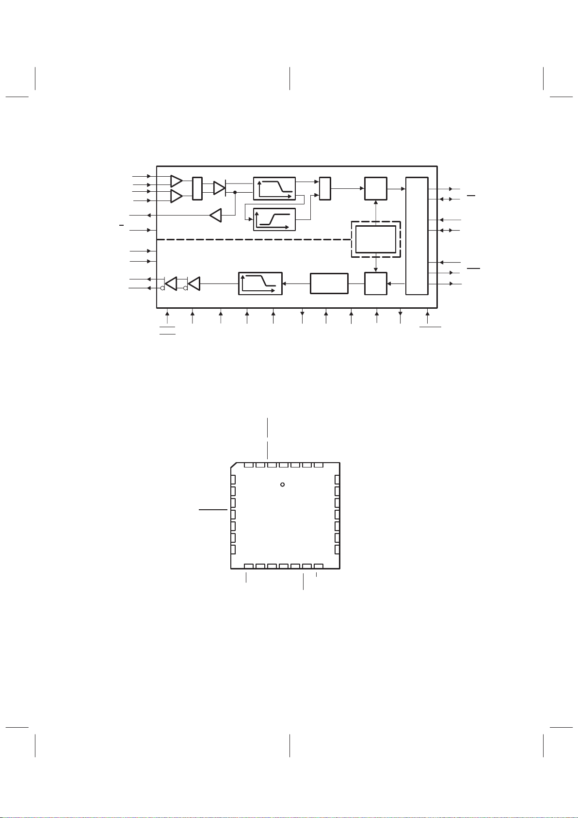
1.2 Functional Block Diagram
DAC Channel
OUT–
OUT+
AUX IN–
AUX IN+
IN–
IN+
DAC
EOC
FSD
DIN
SCLK
MCL
K
DOUT
FS
RESETADC
V
MID
DGTL
GND
DAC
V
DD
PWR
DWN
Correction
(sin x)/x
Port
Serial
Reference
Voltage
Internal
ADC
ADC Channel
M
U
X
X
U
M
Filter
26
25
28
27
3
4
11
12
14
13
10
17
19
25 923 8
Filter
M/S
15
16
18
FC0
FC1
DAC
GND
720
DGTL
V
DD
ADC
V
DD
24
ADC
GND
22
SUBS21DAC
V
MID
6
1
MON OUT
Terminal numbers shown are for the FN package.
1.3 Terminal Assignments
321
13 14
5
6
7
8
9
10
11
IN–
ADC V
DD
ADC V
MID
ADC GND
SUBS
DGTL GND
EOC
DAC V
DD
DAC V
MID
DAC GND
RESET
DGTL V
DD
DIN
DOUT
4
15 16 17 18
SCLK
MCLK
FC0
FC1
FSD
M/S
OUT –
OUT +
PWR DWN
MON OUT
FN PACKAGE
(TOP VIEW)
28 27 26
25
24
23
22
21
20
19
12
FS
AUX IN +
AUX IN –
IN +
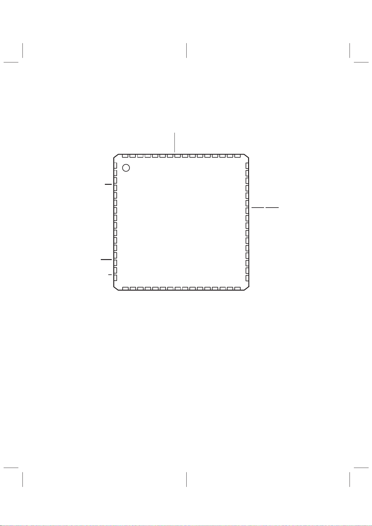
1–4
1.3 Terminal Assignments (Continued)
18 19
NC
NC
OUT–
NC
NC
OUT+
PWR
DWN
NC
MON OUT
NC
AUXIN+
AUXIN–
IN+
IN–
NC
NC
48
47
46
45
44
43
42
41
40
39
38
37
36
35
34
33
20
1
2
3
4
5
6
7
8
9
10
11
12
13
14
15
16
DIN
NC
DOUT
FS
NC
NC
NC
SCLK
NC
MCLK
FC0
FC1
NC
FSD
NC
M/S
21 22 23 24
PM PACKAGE
(TOP VIEW)
NC
DAC GND
63 62 61 60 5964 58
NCNCNC
DGTL VNCRESET
NC
NC
ADC GND
NC
NC
NC
NC
NC
DGTL GND
NC
SUBS
NC
56 55 5457
25 26 27 28 29
53 52
17
EOC
NC
NC
51 50 49
30 31 32
MID
NC
DAC VNCDAC V
NC – No internal connection
NC
NC
NC
DD
MID
DD
ADC V
DD
ADC V
1–5
1.4 Terminal Functions
TERMINAL
NAME NO.†NO.
‡
I/O
DESCRIPTION
ADC V
DD
24 32 I Analog supply voltage for the ADC channel
ADC V
MID
23 30 O Midsupply for the ADC channel (requires a bypass capacitor). ADC V
MID
must be
buffered when used as an external reference.
ADC GND 22 27 I Analog ground for the ADC channel
AUX IN+ 28 38 I Noninverting input to auxiliary analog input amplifier
AUX IN– 27 37 I Inverting input to auxiliary analog input amplifier
DAC V
DD
5 49 I Analog supply voltage for the DAC channel
DAC V
MID
6 51 O Midsupply for the DAC channel (requires a bypass capacitor). DAC V
MID
must be
buffered when used as an external reference.
DAC GND 7 54 I Analog ground for the DAC channel
DIN 10 1 I Data input. DIN receives the DAC input data and command information and is
synchronized with SCLK.
DOUT 11 3 O Data output. DOUT outputs the ADC data results and register read contents.
DOUT is synchronized with SCLK.
DGTL V
DD
9 59 I Digital supply voltage for control logic
DGTL GND 20 22 I Digital ground for control logic
EOC 19 17 O End-of-conversion output. EOC goes high at the start of the ADC conversion
period and low when conversion is complete. EOC remains low until the next ADC
conversion period begins and indicates the internal device conversion period.
FC0 15 11 I Hardware control input. FC0 is used in conjunction with FC1 to request secondary
communication and phase adjustments. FC0 should be tied low if it is not used.
FC1 16 12 I Hardware control input. FC1 is used in conjunction with FC0 to request secondary
communication and phase adjustments. FC1 should be tied low if it is not used.
FS 12 4 I/O Frame synchronization. When FS goes low, DIN begins receiving data bits and
DOUT begins transmitting data bits. In master mode, FS
is low during the
simultaneous 16-bit transmission to DIN and from DOUT. In slave mode, FS
is
externally generated and must be low for one shift-clock period minimum to initiate
the data transfer.
FSD 17 14 O Frame-synchronization delayed output. This active-low output synchronizes a
slave device to the frame synchronization timing of the master device. FSD
is
applied to the slave FS
input and is the same duration as the master FS signal but
delayed in time by the number of shift clocks programmed in the FSD
register.
IN+ 26 36 I Noninverting input to analog input amplifier
IN– 25 35 I Inverting input to analog input amplifier
MCLK 14 10 I The master-clock input drives all the key logic signals of the AIC.
MON OUT 1 40 O The monitor output allows monitoring of analog input and is a high-impedance
output.
M/S 18 16 I Master/slave select input. When M/S is high, the device is the master and when
low, it is a slave.
†
Terminal numbers shown are for the FN package.
‡
Terminal numbers shown are for the PM package.
1–6
1.4 Terminal Functions (Continued)
TERMINAL
NAME NO.†NO.
‡
I/O
DESCRIPTION
OUT+ 3 43 O Noninverting output of analog output power amplifier. OUT+ can drive transformer
hybrids or high-impedance loads directly in a differential connection or a
single-ended configuration with a buffered V
MID
.
OUT– 4 46 O Inverting output of analog output power amplifier. OUT– is functionally identical
with and complementary to OUT+.
PWR DWN 2 42 I Power-down input. When PWR DWN is taken low, the device is powered down
such that the existing internally programmed state is maintained. When PWR
DWN is brought high, full operation resumes.
RESET 8 57 I Reset input that initializes the internal counters and control registers. RESET
initiates the serial data communications, initializes all of the registers to their
default values, and puts the device in a preprogrammed state. After a low-going
pulse on RESET
, the device registers are initialized to provide a 16-kHz
data-conversion rate and 7.2-kHz filter bandwidth for a 10.368-MHz master clock
input signal.
SCLK 13 8 I/O Shift clock. SCLK clocks the digital data into DIN and out of DOUT during the
frame-synchronization interval. When configured as an output (M/S
high), SCLK
is generated internally by dividing the master clock signal frequency by four. When
configured as an input (M/S
low), SCLK is generated externally and
synchronously to the master clock. This signal clocks the serial data into and out
of the device.
SUBS 21 24 I Substrate connection. SUBS should be tied to ADC GND.
†
Terminal numbers shown are for the FN package.
‡
Terminal numbers shown are for the PM package.
1–7
A Register
(8 bits)
Divide by 2
576 kHz
B Register
(8 bits)
Divide by 4
1.296 MHz
2.592 MHz
5.184 MHz
10.368 MHz
MCLK
Processor
SCLK
A Register + A′ Register
(8 bits)
2s Complement
Program Divide
A Counter
(8 bits)
B Counter
288 kHz
FCLK [low-pass filter and
(sin x)/x filter clock]
Conversion
Rate
Single, A-Counter
Period
One-Shot
Phase ShiftNormal
Control
Figure 1–1. Control Flow Diagram
Table 1–1. Operating Frequencies
FCLK
(kHz)
LOW-PASS FILTER
BANDWIDTH
(kHz)
B REGISTER CONTENTS
(Program No. of Filter Clocks)
(Decimal)
CONVERSION
RATE
(kHz)
HIGH-PASS
POLE FREQUENCY
(Hz)
144 3.6 20 (see Note 1)
18
15
10 (see Note 2)
7.2
8
9.6
14.4
36
40
48
72
288 7.2 20 (see Note 1)
18
15
10 (see Notes 2 and 3)
14.4
16
19.2
28.8
72
80
96
144
432 10.8 20 (see Note 1)
18
15 (see Note 3)
10 (see Notes 2 and 3)
21.6
24
28.8
43.2
108
120
144
216
NOTES: 1. The B register can be programmed for values greater than 20; however, since the sample rate is lower than
7.2 kHz and the internal filter remains at 3.6 kHz, an external antialiasing filter is required.
2. When the B register is programmed for a value less than 10, the ADC and the DAC conversions are not
completed before the next frame-sync signal and the results are in error.
3. The maximum sampling rate for the ADC channel is 43.2 kHz. The maximum rate for the DAC channel is
25 kHz.

1–8
1.5 Register Functional Summary
There are nine data registers that are used as follows:
Register 0 The No-op register. The 0 address allows phase adjustments to be made without
reprogramming a data register.
Register 1 The A register controls the count of the A counter.
Register 2 The B register controls the count of the B counter.
Register 3 The A
′ register controls the phase adjustment of the sampling period. The adjustment is
equal to the register value multiplied by the input master period.
Register 4 The amplifier gain register controls the gains of the input, output, and monitor amplifiers.
Register 5 The analog configuration register controls:
• The addition/deletion of the high-pass filter to the ADC signal path
• The enable/disable of the analog loopback
• The selection of the regular inputs or auxiliary inputs
• The function that allows processing of signals that are the sum of the regular inputs and
the auxiliary inputs (V
IN
+ V
AUX IN
)
Register 6 The digital configuration register controls:
• Selection of the free-run function
• FSD
[frame-synchronization (sync) delay] output enable/disable
• Selection of 16-bit function
• Forcing secondary communications
• Software reset
• Software power down
Register 7 The frame-sync delay register controls the time delay between the master-device frame
sync and slave-device frame sync. Register 7 must be the last register programmed when
using slave devices since all register data is latched and valid on the sixteenth falling edge
of SCLK. On the sixteenth falling edge of SCLK, all delayed frame-sync intervals are shifted
by this programmed amount.
Register 8 The frame-sync number register informs the master device of the number of slaves that are
connected in the chain. The frame-sync number is equal to the number of slaves plus one.

2–1
2 Detailed Description
2.1 Definitions and Terminology
ADC Channel All signal processing circuits between the analog input and the digital conversion
results at DOUT
Codec Mode The operating mode under which the device receives shift clock and frame-sync
signals from a host processor. The device has no slaves.
d The d represents valid programmed or default data in the control register format
(see Section 2.19) when discussing other data-bit portions of the register.
Dxx Bit position in the primary data word (xx is the bit number)
DAC Channel All signal processing circuits between the digital data word applied to DIN and the
differential output analog signal available at OUT+ and OUT–
Data Transfer Interval The time during which data is transferred from DOUT and to DIN. This interval is 16
shift clocks regardless of whether the shift clock is internally or externally generated.
The data transfer is initiated by the falling edge of the frame-sync signal.
DSxx Bit position in the secondary data word (xx is the bit number)
FCLK An internal clock frequency that is a division of MCLK that controls the low-pass filter
and (sinx)/x filter clock (see Figure 1–1 and Table 1-1).
f
i
The analog input frequency of interest
Frame Sync The falling edge of the signal that initiates the data-transfer interval. The primary
frame sync starts the primary communications, and the secondary frame sync starts
the secondary communications.
Frame Sync and The time between falling edges of successive primary frame-sync signals
Sampling Period
Frame-Sync Interval The time period occupied by 16 shift clocks. Regardless of the mode of operation,
there is always an internal frame-sync interval signal that goes low on the rising
edge of SCLK and remains low for 16 shift clocks. It is used for synchronization of
the serial-port internal signals. It goes high on the seventeenth rising edge of SCLK.
f
s
The sampling frequency that is the reciprocal of the sampling period.
Host Any processing system that interfaces to DIN, DOUT, SCLK, or FS
.
Master Mode The operating mode under which the device generates and uses its own shift clock
and frame-sync signal and generates all delayed frame-sync signals necessary to
support slave devices.
Phase Adjustment The programmed time variation from the falling edge of one frame-sync signal to the
falling edge of the next frame sync signal. The time variation is determined by the
contents of the A
′ register. Since the time between falling edges of successive
frame-sync signals is the the sampling period, the sampling period is adjusted.
Primary (Serial) The digital data-transfer interval. Since the device is synchronous, the signal data
Communications words from the ADC channel and to the DAC channel occur simultaneously.
Secondary (Serial) The digital control and configuration data-transfer interval into DIN and the register
Communications read-data cycle from DOUT. The data-transfer interval occurs when requested by
hardware or software.
Signal Data The input signal and all of the converted representations through the ADC channel
and return through the DAC channel to the analog output. This is contrasted with
the purely digital software-control data.
Slave Mode The operating mode under which the device receives shift clock and frame-sync
signals from a master device.

2–2
Stand-Alone Mode The operating mode under which the device generates and uses its own shift clock
and frame-sync signal. The device has no slave devices.
X The X represents a don’t-care bit position within the control register format.
2.2 Reset and Power-Down Functions
2.2.1 Reset
The TLC320AC01 resets both the internal counters and registers, including the programmed registers, by
any of the following:
• Applying power to the device, causing a power-on reset (POR)
• Applying a low reset pulse to RESET
• Reading in the programmable software reset bit (DS01 in register 6)
PWR
DWN resets the counters only and preserves the programmed register contents.
2.2.2 Conditions of Reset
The two internal reset signals used for the reset and synchronization functions are as follows:
1. Counter reset: This signal resets all flip-flops and latches that are not externally programmed with
the exception of those generating the reset pulse itself. In addition, this signal resets the software
power-down bit.
Counter reset = power-on reset + RESET
+ RESET bit + PWR DWN
2. Register reset: This signal resets all flip-flops and latches that are not reset by the counter reset
except those generating the reset pulse itself.
Register reset = power-on reset + RESET
+ RESET bit
Both reset signals are at least one master-clock period long and release on the falling edge of the master
clock.
2.2.3 Software and Hardware Power-Down
Given the definitions and conditions of RESET , the software-programmed power-down condition is cleared
by resetting the software bit (DS00 in register 6) to zero. It is also cleared by either cycling the power to the
device, bringing PWR
DWN low, or bringing RESET low.
PWR
DWN powers down the entire chip ( < 1 mA ). The software-programmable power-down bit only
powers down the analog section of the chip ( < 3 mA ), which allows a software power-up function. Cycling
PWR
DWN high to low and back to high resets all flip-flops and latches that are not externally programmed,
thereby preserving the register contents.
When PWR
DWN is not used, it should be tied high.
2.2.4 Register Default Values After POR, Software Reset, or RESET Is Applied
Register 1 – The A Register
The default value of the A-register data is decimal 18 as shown below.
DS07 DS06 DS05 DS04 DS03 DS02 DS01 DS00
0 0 0 1 0 0 1 0
2–3
Register 2 – The B Register
The default value of the B-register data is decimal 18 as shown below.
DS07 DS06 DS05 DS04 DS03 DS02 DS01 DS00
0 0 0 1 0 0 1 0
Register 3 – The A′ Register
The default value of the A
′-register data is decimal 0 as shown below.
DS07 DS06 DS05 DS04 DS03 DS02 DS01 DS00
0 0 0 0 0 0 0 0
Register 4 – The Amplifier Gain-Select Register
The default value of the amplifier gain-select register data is shown below.
DS07 DS06 DS05 DS04 DS03 DS02 DS01 DS00
0 0 0 0 0 1 0 1
Register 5 – The Analog Control-Configuration Register
The power-up and reset conditions are as shown below. In the read mode, 8 bits are read but the 4 LSBs
are repeated as the 4 MSBs.
DS03 DS02 DS01 DS00
0 0 0 1
Register 6 – The Digital Configuration Register
The default value of DS07 – DS00 is 0 as shown below.
DS07 DS06 DS05 DS04 DS03 DS02 DS01 DS00
0 0 0 0 0 0 0 0
Register 7 – The Frame-Sync Delay Register
The default value of DS07 – DS00 is 0 as shown below.
DS07 DS06 DS05 DS04 DS03 DS02 DS01 DS00
0 0 0 0 0 0 0 0
Register 8 – The Frame-Sync Number Register
The default value of DS07 – DS00 is 1 as shown below.
DS07 DS06 DS05 DS04 DS03 DS02 DS01 DS00
0 0 0 0 0 0 0 1

2–4
2.3 Master-Slave Terminal Function
Table 2–1 describes the function of the master/slave (M/S) input. The only difference between master and
slave operations in the TLC320AC01 is that SCLK and FS
are outputs when M/S is high and inputs when
M/S
is low.
Table 2–1. Master-Slave Selection
MODE M/S
†
FS SCLK
Master and Stand Alone H Output Output
Slave and Codec Emulation L Input Input
†
When the stand-alone mode is desired or when the device is
permanently in the master mode, M/S
must be high.
2.4 ADC Signal Channel
To produce excellent common-mode rejection of unwanted signals, the analog signal is processed
differentially until it is converted to digital data. The signal is amplified by the input amplifier at one of three
software-selectable gains (typically 0 dB, 6 dB, or 12 dB). A squelch mode can also be programmed for the
input amplifier.
The amplifier output is filtered and applied to the ADC input. The ADC converts the signal into discrete digital
words in 2s-complement format corresponding to the analog-signal value at the sampling time. These 16-bit
digital words, representing sampled values of the analog input signal, are clocked out of the serial port
(DOUT), one word for each primary communication interval. During secondary communications, the data
previously programmed into the registers can be read out with the appropriate register address and with the
read bit set to 1. When a register read is not requested, all 16 bits are 0.
2.5 DAC Signal Channel
DIN receives the 16-bit serial data word (2s complement) from the host during the primary communications
interval and latches the data on the seventeenth rising edge of SCLK. The data are converted to an analog
voltage by the DAC with a sample and hold and then through a (sin x)/x correction circuit and a smoothing
filter. An output buffer with three software-programmable gains (0 dB, –6 dB, and –12 dB), as shown in
register 4, drives the differential outputs OUT+ and OUT–. A squelch mode can also be programmed for
the output buffer. During secondary communications, the configuration program data are read into the
device control registers.
2.6 Serial Interface
The digital serial interface consists of the shift clock, the frame-synchronization signal, the ADC-channel
data output, and the DAC-channel data input. During the primary 16-bit frame-synchronization interval, the
SCLK transfers the ADC channel results from DOUT and transfers 16-bit DAC data into DIN.
During the secondary frame-synchronization interval, the SCLK transfers the register read data from DOUT
when the read bit is set to a 1. In addition, the SCLK transfers control and device parameter information into
DIN. The functional sequence is shown in Figure 2–1.
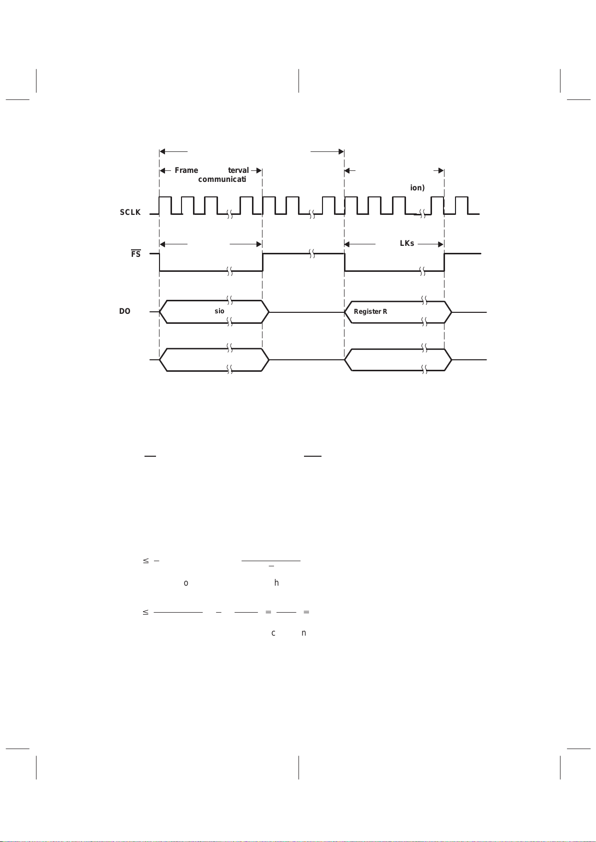
2–5
Register Read Data or All 0s
ADC Conversion Result
DAC Input Data
Control and Device Parameter
Data
16 SCLKs
16 SCLKs
Frame-Sync Interval
(primary communication)
Frame-Sync Interval
(secondary
communication)
SCLK
FS
DOUT
DIN
[ (B register)/2] FCLK Periods
†
†
The time between the primary and secondary frame sync is the time equal to filter clock (FCLK) period multiplied by the
B-register contents divided by two. The time interval is rounded to the nearest shift clock. The secondary frame-sync
signal goes from high to low on the next shift clock low-to-high transition after (B register/2) filter clock periods.
Figure 2–1. Functional Sequence for Primary and Secondary Communication
2.7 Number of Slaves
The maximum number of slaves is determined by the sum of the individual device delays from the
frame-sync (FS
) input low to the frame-sync delayed (FSD) low for all slaves according to equation 1:
(n) / tp(FS–FSD) < 1/2 shift-clock period
(1)
Where:
n is the number of slave devices.
Example:
From equation 1 above, the number of slaves is given by equation 2:
(n)
v
1
2
x (SCLK period) x
1
tp(FS*FSD
)
(2)
assuming the master clock is 10.368 MHz and the shift clock is 2.5965 MHz and tp(FS – FSD) is 40 ns, then
according to equation 3, the number of slaves is:
n
v
1
2.
5965
MHz
x
1
2
x
1
40 ns
+
1000
192
+
4.8
(3)
The maximum number of slaves under these conditions is four.
2–6
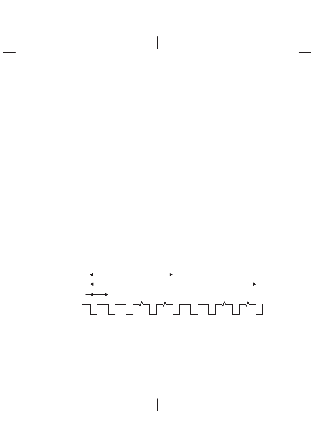
2.8 Required Minimum Number of MCLK Periods
Master with slave operation is summarized in the following sections.
2.8.1 TLC320AC01 AIC Master-Slave Summary
After initial setup and the master and slave frame syncs are separated, when secondary communication is
needed for a slave device, a 1 1 must be placed in the 2 LSBs of each primary data word for all devices in
the system, master and slave, by the host processor. In other words, all AICs must receive secondary frame
requests.
The host processor must issue the command by setting D01 and D00 to a 1 in the primary frame sync data
word of all devices. Then the master generates the master primary frame sync and, after the number of shift
clocks set by the FSD register value, the slave primary frame sync intervals. Then, after (B register value/2)
FCLK periods, the master secondary frame sync occurs first, and then the slave secondary frame sync
occurs. These are also rippled through the slave devices.
In other words, when a secondary communications interval is requested by the host processor as described
above:
1. The master outputs the master primary frame sync interval, and then the slave primary frame
sync intervals after the FSD register value number of shift clocks.
2. After (B register value/2) FCLK periods, the master then outputs the master secondary frame
sync interval, and after the FSD register value number of shift clocks, the slave secondary frame
sync intervals.
This sequence is shown in Figure 2–2.
The host must keep track of whether the master or a slave is then being addressed and also the number
of slave devices. The master always outputs a 00 in the last 2 bits of the DOUT word, and a slave always
outputs a 1 in the LSB of the DOUT word. This information allows the system to recognize a starting point
by interrogating the least significant bit of the DOUT word. If the LSB is 0, then that device is the master,
and the system is at the starting point.
Note: This identification always happens except in 16-bit mode when the 2 LSBs are not available
for identification purposes.
Sampling Period
(B Register Value/2) FCLK Periods
FSD Value
in SCLKs
Frame Sync
Sequence
MP SP1 SP2 SPn MS SS1 SS2 SSn MP
Period Symbol
Periods shown: Each period must be a minimum of 16 SCLKs plus 2 additional SCLKs
MP = Master Primary Period
SP1 = 1st Slave Primary Period
SP2 = 2nd Slave Primary Period
SPn = nth Slave Primary Period
MS = Master Secondary Period
SS1 = 1st Slave Secondary Period
SS2 = 2nd Slave Secondary Period
SSn = nth Slave Secondary Period
Figure 2–2. Timing Sequence
2–7
2.8.2 Notes on TLC320AC01/02 AIC Master-Slave Operation
Master/slave operational detail is summarized in the following notes:
1. The slave devices can be programmed independently of the master as long as the clock divide
register numbers are not changed. The gain settings, for example, can be changed
independently.
2. The method that is used to program a slave independently is to request a secondary
communication of the master and all slaves and ripple the delayed frame sync to the desired slave
device to be programmed.
3. Secondary frame syncs must be requested for all devices in the system or none. This is required
so that the master generates secondary frames for the slaves and allows the slaves to know that
the second frame syncs they receive are secondary frame syncs. Each device in the system must
receive a secondary frame request in its corresponding primary frame sync period (11 in the last
2 LSBs).
4. Calculation of the sampling frequency in terms of the master clock and the shift clock and the
respective register ratios is (see equations 4–6):
Sampling frequency+f
s
+
FCLK
B register value
+
f(MCLK
)
2 (A register value)
(B register value
)
(4)
Therefore,
f(MCLK
)
f
s
+2 (A register value) (B register value
)
(5)
and in terms of the shift clock frequency, since
(6)
f(SCLK)
f
s
+
(A register value)
(B register value
)
2
+
Number of SCLK periods
Sampling period
f(MCLK)+4 f(SCLK)
then
5. The minimum number of shift clocks between falling edges of any two frame syncs is 18 because
the frame sync delay register minimum number is 18.
When a secondary communication is requested by the host, the master secondary frame sync
begins at the middle of the sampling period (followed by the slave secondary frame syncs), so all
primary frame sync intervals (master and slave) must occur within one-half the sampling time.
2–8
The first secondary frame-sync falling edge, therefore, occurs at the following time (see
equation 7):
Time to first secondary frame sync
+
B register value
2
(
FCLK periods)+
(7)
A register value B register value (number of MCLK periods)
+
A register value B register value
4
(number of SCLK periods)
6. Number of frame sync intervals using equation 8.
All master and slave primary frame sync intervals must occur within the time of equation 7.
Since 18 shift clocks are required for each frame sync interval, then the number of frame sync
intervals from equation 8 is:
Number of frame sync intervals
+
A register value B register value
4 18 (SCLKsńframe sync interval)
(8
)
+
A register value B register value
72
7. Number of devices, master and slave, in terms of f(MCLK) and fs.
Substituting the value from equation 5 for the A ×B register value product gives the total number
of devices, including the master and all slaves that can be used, for a given master clock and
sampling frequency . Therefore, using equation 9:
Number of devices
+
f(MCLK)
144 f
s
(9)
8. Number of devices, master and slave, if slave devices are reprogrammed.
Equation 9 does not include reprogramming the slave devices after the frame sync delay occurs.
So if programming is required after shifting the slave frame syncs by the FSD register, then the
total number of devices is given by equation 10 is:
Number of devices
+
f(MCLK)
288 f
s
(10)
9. Example of the maximum number of devices if the slave devices are reprogrammed assuming
the following values:
f(MCLK)+10.368 MHz, f
s
+
8kHz
then from equation 10,
Maximum number of devices
+
10.368 MHz
288
(
8kHz
)
+
4.5
therefore, one master and three slaves can be used.
2–9
2.9 Operating Frequencies
2.9.1 Master and Stand-Alone Operating Frequencies
The sampling (conversion) frequency is derived from the master-clock (MCLK) input by equation 11:
fs+
Sampling (conversion) frequency
+
MCLK
(A register value) (B register value) 2
(11)
The inverse is the time between the falling edges of two successive primary frame-synchronization signals.
The input and output data clock (SCLK) frequency is given in equation 12:
SCLK frequency
+
MCLK frequency
4
(12)
2.9.2 Slave and Codec Operating Frequencies
The slave operating frequencies are either the default values or programmed by the control data word from
the master and codec conversion and the data frequencies are determined by the externally applied SCLK
and FS
signals.
2.10 Switched-Capacitor Filter Frequency (FCLK)
The filter clock (FCLK) is an internal clock signal that determines the filter band-pass frequency and is the
B counter clock. The frequency of the filter clock is derived by equation 13:
FCLK
+
MCLK
(A register value) 2
(13)
2.11 Filter Bandwidths
The low-pass (LP) filter –3 dB corner is derived in equation 14:
f(LP)
+
FCLK
40
+
MCLK
40 (A register value) 2
(14)
The high-pass (HP) filter –3 dB corner is derived in equation 15:
f(HP)
+
Sampling frequency
200
+
MCLK
200 2 (A register value) (B register value)
(15)
2.12 Master and Stand-Alone Modes
The difference between the master and stand-alone modes is that in the stand-alone mode there are no
slave devices. Functionally these two modes are the same. In both, the AIC internally generates the shift
clock and frame-sync signal for the serial communications. These signals and the filter clock (FCLK) are
derived from the input master clock.The master clock applied at the MCLK input determines the internal
device timing. The shift clock frequency is a divide-by-four of the master clock frequency and shifts both the
input and output data at DIN and DOUT, respectively, during the frame-sync interval (16 shift clocks long).
To begin the communication sequence, the device is reset (see Section 2.2.1), and the first frame sync
occurs approximately 648 master clocks after the reset condition disappears.
2.12.1 Register Programming
All register programming occurs during secondary communications, and data is latched and valid on the
sixteenth falling edge of SCLK. After a reset condition, eight primary and secondary communications cycles
are required to set up the eight programmable registers. Registers 1 through 8 are programmed in
secondary communications intervals 1 through 8, respectively. If the default value for a particular register
is desired, that register does not need to be addressed during the secondary communications. The no-op
command addresses the pseudo-register (register 0), and no register programming takes place during this
communications. The no-op command allows phase shifts of the sampling period without reprogramming
any register.
During the eight register programming cycles, DOUT is in the high-impedance state. DOUT is released on
the rising edge of the eighth primary internal frame-sync interval. In addition, each register can be read back

2–10
during DOUT secondary communications by setting the read bit to 1 in the appropriate register. Since the
register is in the read mode, no data can be written to the register during this cycle. To return this register
to the write mode requires a subsequent secondary communication (see Section 2.19 for detailed register
description).
2.12.2 Master and Stand-Alone Functional Sequence
The A counter counts according to the contents of the A register, and the A counter frequency is divided by
two to produce the filter clock (FCLK). The B counter is clocked by FCLK with the following functional
sequence:
1. The B counter starts counting down from the B register value minus one. Each count remains in
the counter for one FCLK period including the zero count. This total counter time is referred to
as the B cycle. The end of the zero count is called the end of B cycle.
2. When the B counter gets to a count of nine, the analog-to-digital (A-to-D) conversion starts.
3. The A-to-D conversion is complete ten FCLK periods later.
4. FS
goes low on a rising edge of SCLK after the A-to-D conversion is complete. That rising edge
of SCLK must be preceded by a falling edge of SCLK, which is the first falling edge to occur after
the end of B cycle.
5. The D-to-A conversion cycle begins on the rising edge of the internal frame-sync interval and is
complete ten FCLK periods later.
2.13 Slave and Codec Modes
The only difference between the slave and codec modes is that the codec mode is controlled directly by the
host and does not use a delayed frame-sync signal. In both modes, the shift clock and the frame sync are
both externally generated and must be synchronous with MCLK. The conversion frequency is set by the time
interval of externally applied frame-sync falling edges except when the free-run function is selected by bit 5
of register 6 (see Section 2.15.4). The slave device or devices share the shift clock generated by the master
device but receive the frame sync from the previous slave in the chain. The Nth slave FS
receives the
(N–1)st slave FSD
output and so on. The first slave device in the chain receives FSD from the master.

2–11
2.13.1 Slave and Codec Functional Sequence
The A counter counts according to the contents of the A register, and the A counter frequency is divided by
two to produce the FCLK. The device function in the slave or codec mode is the same as steps 1 through
3 of the B cycle description in the master mode but differs as follows:
1. Same as master
2. Same as master
3. Same as master
4. All internal clocks stop 1/2 FCLK before the end of count 0 in the B counter cycle.
5. All internal clocks are restarted on the first rising edge of MCLK after the external FS
input goes
low. This operation provides the synchronization necessary when using an external FS
signal.
6. The D-to-A conversion starts on the rising edge of the internally generated frame-sync interval
at the end of the 16-shift clock data transfer.
In the slave mode, the master controls the phase adjustments for itself and all slaves since all devices are
programmed in the same frame-sync interval. In the codec mode, the shift clock and frame sync are
externally generated and provide the timing for the ADC and DAC if the free-run function has not been
selected (see Subsection 2.15.4). In the codec mode, there is usually no need for phase adjustments;
however, any required phase adjustments must be made by adjusting the external frame-sync timing
(sampling time).
2.13.2 Slave Register Programming
When slave devices are used on power-up or reset, all slave frame-sync signals occur at the same time as
the master frame-sync signal and all slave devices are programmed during the master secondary framesync interval with the same data as the master. The last register programmed must be the frame-sync delay
(FSD) register because the delay starts immediately on the rising edge of the seventeenth shift clock of that
frame- sync interval. After the FSD register programming is completed for the master and slave, the slave
primary frame interval is shifted in time (time slot allocated) according to the data contained in the slave FSD
registers. The master then generates frame-sync intervals for itself and each slave to synchronize the host
serial port for data transfers for itself and all slave devices.
The number of slaves is specified in the FSN register (register 8); therefore, the number of frame-sync
intervals generated by the master is equal to the number of slaves plus one (see Section 2.7). These master
frame-sync intervals are separated in time by the delay time specified by the FSD register (register 7). These
master-generated intervals are the only frame-sync interval signals applied to the host serial port to provide
the data-transfer time slot for the slave devices.
2.14 Terminal Functions
2.14.1 Frame-Sync Function
The frame-sync signal indicates that the device is ready to send and receive data for both master and slave
modes. The data transfer begins on the falling edge of the frame-sync signal.
2.14.1.1 Frame Sync (FS), Master Mode
The frame sync is generated internally. FS goes low on the rising edge of SCLK and remains low for the
16-bit data transfer. In addition to generating its own frame-sync interval, the master also outputs a frame
sync for each slave that is being used.

2–12
2.14.1.2 Frame-Sync Delayed (FSD), Master Mode
For the master, the frame-sync delayed output occurs 1/2 shift-clock period ahead of FS to compensate for
the time delay through the master and slave devices. The timing relationships are as follows:
1. When the FSD register data is 0, then FSD
goes low on the falling edge of SCLK prior to the rising
edge of SCLK when FS goes low (see Figure 4–4).
2. When the FSD register data is greater than 17, then FSD
goes low on a rising edge of SCLK that
is the FSD register number of SCLKs after the falling edge of FS.
Register data values from 1 to 17 should not be used.
2.14.1.3 Frame Sync (FS), Slave Mode
The frame-sync timing is generated externally, applied to FS, and controls the ADC and DAC timing (see
Subsection 2.15.4). The external frame-sync width must be a minimum of one shift clock to be recognized
and can remain low until the next data frame is required.
2.14.1.4 Frame-Sync Delayed (FSD), Slave Mode
This output is fed from the master to the first slave and the first slave FSD output to the second and so on
down the chain. The FSD timing sequence in the slave mode is as follows:
1. When the FSD register data is 0, then FSD
goes low after FS goes low (see Figure 4–5).
2. When the FSD register data is greater than 17, FSD
goes low on a rising edge of SCLK that is
the FSD register number of SCLKs after the falling edge of FS.
Data values from 1 to 17 should not be used.
2.14.2 Data Out (DOUT)
DOUT is placed in the high-impedance state on the seventeenth rising edge of SCLK (internal or external)
after the falling edge of frame sync. In the primary communication, the data word is the ADC conversion
result. In the secondary communication, the data is the register read results when requested by the
read/write (R/W
) bit with the eight MSBs set to 0 (see Section 2.16). If no register read is requested, the
secondary word is all zeroes.
2.14.2.1 Data Out, Master Mode
In the master mode, DOUT is taken from the high-impedance state by the falling edge of frame sync. The
most significant data bit then appears on DOUT.
2.14.2.2 Data Out, Slave Mode
In the slave mode, DOUT is taken from the high-impedance state by the falling edge of the external frame
sync or the rising edge of the external SCLK, whichever occurs first (see Figure 4–7). The falling edge of
frame sync can occur
± 1/4 SCLK period around the SCLK rising edge (see Figure 4– 3). The most
significant data bit then appears on DOUT.
2.14.3 Data In (DIN)
In the primary communication, the data word is the digital input signal to the DAC channel. In the secondary
communication, the data is the control and configuration data to set up the device for a particular function
(see Section 2.16).
2.14.4 Hardware Program Terminals (FC1 and FC0)
These inputs provide for hardware programming requests for secondary communication or phase
adjustment. These inputs work in conjunction with the control bits D01 and D00 of the primary data word
or control bits DS15 and DS14 of the secondary data word. The data on FC1 and FC0 are latched on the
rising edge of the next internally generated primary or secondary frame-sync interval. These inputs should
be tied low if not used (see Section 2.17 and Table 2–3).
2–13
2.14.5 Midpoint Voltages (ADC V
MID
and DAC V
MID
)
Since the device operates at a single-supply voltage, two midpoint voltages are generated for internal signal
processing. ADC V
MID
is used for the ADC channel reference, and DAC V
MID
is used for the DAC channel
reference. Two references minimize channel-to-channel noise and crosstalk. ADC V
MID
and DAC V
MID
must be buffered when used as a reference for external signal processing.
2.15 Device Functions
2.15.1 Phase Adjustment
In some applications, such as modems, the device sampling period may require an adjustment to
synchronize with the incoming bit stream to improve the signal-to-noise ratio. The TLC320AC01 can adjust
the sampling period through the use of the A
′ register and the control bits.
2.15.1.1 Phase-Adjustment Control
A phase adjustment is a programmed variation in the sampling period. A sampling period is adjusted
according to the data value in the A
′ register, and the phase adjustment is that number of master clocks
(MCLK). An adjustment is made during device operation with data bits D01 and D00 in the primary
communication, with data bits DS15 and DS14 in the secondary word or in combination with the hardware
terminals FC1 and FC0 (see Table 2–3). This adjustment request is latched on the rising edge of the next
internal frame-sync interval and is only valid for the next sampling period. To repeat the phase adjustment,
another phase request must be initiated.
2.15.1.2 Use of the A′ Register for Phase Adjustment
The A′ register value makes slight timing adjustments to the sampling period. The sampling period
increases or decreases according to the sign of the programmed A
′ register value and the state of data bits
D01 and D00 in the primary data word.
The general equation for the conversion frequency is given in equation 16:
+
MCLK
(2 A register value B register value)"(AȀregister value)
fs = conversion frequency
(16)
Therefore, if A
′ = 0, the device conversion (sampling) frequency and period is constant.
If a nonzero A
′ value is programmed, the sampling frequency and period responds as shown in T able 2–2.
Table 2–2. Sampling Variation With A′
SIGN OF THE A′ REGISTER VALUE
D01 D00
PLUS VALUE
(+)
NEGATIVE VALUE
(–)
0
1
(increase command)
Frequency decreases,
period increases
Frequency increases,
period decreases
1
0
(decrease command)
Frequency increases,
period decreases
Frequency decreases,
period increases
An adjustment to the sampling period, which must be requested through D01 and D00 of the primary data
word to DIN, is valid for the following sampling period only. When the adjustment is required for the
subsequent sampling period, it must be requested again through D01 and D00 of the primary data word.
For each request, only the sampling period occurring immediately after the primary data word request is
affected.

2–14
The amount of time shift in the entire sampling period (1/fs) is as follows:
When the sampling period is set to 125 µs (8 kHz), the A′ register is loaded with decimal 10 and the
TLC320AC01 master clock frequency is 10.386 MHz. The amount of time each sampling period is increased
or decreased, when requested, is given in equation 17:
Time shift = (A
′ register value) × (MCLK period) (17)
The device changes the entire sampling period by only the MCLK period times the A
′ register value as given
in equation 18:
Change in sampling period = contents of A
′ register × master clock period
= 10
× 96.45 ns = 964 ns (less than 1% of the sampling period) (18)
The sampling period changes by 964.5 ns each time the phase adjustment is requested by the primary data
word (i.e., once per sampling period).
It is evident then that the change in sampling period is very small compared to the sampling period. To
observe this effect over a long period of time ( > sampling period), this change must be continuously
requested by the primary data word. If the adjustment is not requested again, the sampling period changes
only once and it may appear that there was no execution of the command. This is especially true when bench
testing the device. Automatic test equipment can test for results within a single sampling period.
Internally, the A
′ register value only affects one cycle (period) of the A counter. The A and A′ values are
additive, but only for one A-counter period. The A counter begins the first count at the default or programmed
A-register value and counts down to the A
′-register value. As the A′ value increases or decreases, the first
clock cycle from the A counter is lengthened or shortened. The initial A-counter period is the only counter
period affected by the A
′ register such that only this single period is increased or decreased.
2.15.2 Analog Loopback
This function allows the circuit to be tested remotely. In loopback, OUT+ and OUT– are internally connected
to IN+ and IN–. The DAC data bits D15 to D02 that are applied to DIN can be compared with the ADC output
data bits D15 to D02 at DOUT. There are some differences due to the ADC and DAC channel offset. The
loopback function is implemented by setting DS01 and DS00 to zero in control register 5 (see Section 2.19).
When analog loopback is enabled, the external inputs to IN+ and IN– are disconnected, but the signals at
OUT+ and OUT– may still be read.
2.15.3 16-Bit Mode
In the 16-bit mode, the device ignores the last two control bits (D01 and D00) of the primary word and
requests continual secondary communications to occur. By ignoring the last two primary communication
bits, compatibility with existing 16-bit software can be maintained. This function is implemented by setting
bit DS03 to 1 in register 6. To return to normal operation, DS03 must be reprogrammed to 0.
2.15.4 Free-Run Mode
With the free-run bit set in register 6, the external shift clock and frame sync control only the data transfer.
The ADC and DAC timing are controlled by the A and B register values, and the phase-shift adjustment must
be done as if the device is in stand-alone mode (by the software or the state of FC1 and FC0).
Phase adjustment cannot be made by adjustment of the frame-sync timing. The external frame sync must
occur within 1/2 FCLK period of the internal frame sync (FCLK as determined by the values of the A and
B registers).
When the external frame sync occurs simultaneously with the internal load, the data-transfer request by the
external frame sync takes precedence over an internal load command. The latching of the ADC conversion
data in the output register is inhibited until the current 16 bits are shifted out of the register by the shift clock.
2.15.5 Force Secondary Communication
With bit 2 in register 6 set to 1, secondary communication is requested continuously. It overrides all software
and hardware requests concerning secondary communication. Phase shifting, however, can still be
performed with the software and hardware.

2–15
2.15.6 Enable Analog Input Summing
By setting bits DS01 and DS00 to 11 in register 5, the normal analog input voltage is summed with the
auxiliary input voltage. The gain for the analog input amplifier is set by data bits DS03 and DS02 in register 4.
2.15.7 DAC Channel (sin x)/x Error Correction
The (sin x)/x compensation filter is designed for zero (sin x)/x error using a B-register value of 15. Since the
filter cannot be removed from the signal path, operation using another B-register value results in an error
in the reconstructed analog output. The error is given by equation 19. Any error compensation needed by
a given application can be performed in the software.
DAC channel frequency response error+20 log
10
ȧ
ȧ
ȧ
ȡ
Ȣ
sin
ǒ
2p A
B
f
MCLK
f
Ǔ
sin
ǒ
30p
A
f
MCLK
f
Ǔ
15
B
ȧ
ȧ
ȧ
ȣ
Ȥ
(19)
where:
f = the frequency of interest
f
MCLK
= the TLC320AC01 master-clock frequency
A = the A-register value
B = the B-register value
and the arguments of the sin functions are in radians.
2.16 Serial Communications
2.16.1 Stand-Alone and Master-Mode Word Sequence and Information Content During
Primary and Secondary Communications
For the stand-alone and master modes, the sequence in Figure 2–2 shows the relationship between the
primary and secondary communications interval, the data content into DIN, and the data content from
DOUT.
The TLC320AC01 can provide a phase-shift command or the next secondary communications interval by
decoding 1) the programmed state of the FC1 and FC0 inputs and the D01 and D00 data bits in the primary
data word, or 2) the state of the FC1 and FC0 inputs and the DS15 and DS14 data bits in the secondary
data word (see Table 2–3). When DS13 (the R/W
bit) is the default value of 0, all 16 bits from DOUT are
0 during secondary communication. However, when the R/W
bit is set to 1 in the secondary communication
control word, the secondary transmission from DOUT still contains 0s in the eight MSBs. The lower order
8 bits contain the data of the register currently being addressed. This function provides register status
information for the host.

2–16
DOUT
[ (B register)/2] FCLK Periods
†
Primary Frame Sync
(16 SCLKs long)
Secondary Frame Sync
(16 SCLKs long)
FS
2s-Complement ADC Output
(14 bits plus 00 for the two LSBs)
16 Bits All 0s, Except When in
Read Mode (then least significant
8 bits are register data)
DIN
2s-Complement Input for the DAC
Channel (14 bits plus two
function bits). If the 2 LSBs Are
Set to 1, Secondary Frame Sync Is
Generated by the TLC320AC01
Input Data for the Internal Registers
(16 bits containing control,
address, and data information)
†
The time between the primary and secondary frame sync is the time equal to filter clock (FCLK) period multiplied by the
B-register contents divided by two. The time interval is rounded to the nearest shift clock. The secondary frame-sync
signal goes from high to low on the next shift clock low-to-high transition after (B register/2) filter clock periods.
Figure 2–3. Master and Stand-Alone Functional Sequence
2.16.2 Slave and Codec-Mode Word Sequence and Information Content During
Primary and Secondary Communications
For the slave and codec modes, the sequence is basically the same as the stand-alone and master modes
with the exception that the frame sync and the shift clock are generated and controlled externally as shown
in Figure 2–3. For the codec mode, the frame-sync pulse width needs to be a minimum of one shift clock
long. The timing relationship between the frame sync and shift clock is shown in the timing diagrams. Phase
shifting is usually not required in the slave or codec mode because the frame-sync timing can be adjusted
externally if required.
DOUT
Primary Frame Sync Secondary Frame Sync
FS
2s-Complement ADC Output
(14 bits plus 00 for the 2 LSBs in
master and stand-alone mode and
01 in slave mode)
16 Bits, All 0s, Except When in
Read Mode (then least significant
8 bits are register data)
DIN
2s-Complement Input for the DAC
Channel (14 bits plus two
function bits)
Input Data for the Internal
Registers (16 bits containing
control, address, and data
information)
1 SCLK Minimum1 SCLK Minimum
NOTE A: The time between the primary and secondary frame syncs is determined by the application; however, enough
time must be provided so that the host can execute the required number of software instructions in the time
between the end of the primary data transfer (rising edge of the primary frame-sync interval) and the falling
edge of the secondary frame sync (start of secondary communications).
Figure 2–4. Slave and Codec Functional Sequence

2–17
2.17 Request for Secondary Serial Communication and Phase Shift
The following paragraphs describe a request for secondary serial communication and phase shift using
hardware control inputs FC1 and FC0, primary data bits D01 and D00, and secondary data bits DS15 and
DS14.
2.17.1 Initiating a Request
Combinations of FC1 and FC0 input conditions, bits D01 and D00 in the primary serial data word, FC1 and
FC0, and bits DS15 and DS14 in the secondary serial data word can initiate a secondary serial
communication or request a phase shift according to the following rules (see Table 2–3).
1. Primary word phase shifts can be requested by either the hardware or software when the other
set of signals are 11 or 00. If both hardware and software request phase shifts, the software
request is performed.
2. Secondary words can be requested by either the software or hardware at the same time that the
other set of signals is requesting a phase shift.
3. Hardware inputs FC1 and FC0 are ignored during the secondary word unless DS15 and DS14
are 11. When DS15 and DS14 are 01 or 10, the corresponding phase shift is performed. When
DS15 and DS14 are 00, no phase shift is performed even when the hardware requests a phase
shift.
2.17.2 Normal Combinations of Control
The normal combinations of control are as follows:
1. Use D01 and D00 and DS15 and DS14 to request phase shifts and secondary words by holding
FC1 and FC0 to 00.
2. Use FC1 and FC0 exclusively to request phase shifts and secondary words by holding D01 and
D00 to 00 and DS15 and DS14 to 11.
3. Use D01 and D00 only to request secondary words and FC1 and FC0 to perform phase shifts
once per period by holding DS15 and DS14 to 00.
2.17.3 Additional Control Options
Additional control options are unusual and are rarely needed or used; however, they are as follows:
1. Use D01 and D00 only to request secondary words and FC1 and FC0 to perform phase shifts
twice per period by holding DS15 and DS14 to 11.
2. Use FC1 and FC0 exclusively to request secondary words and D01 and D00 and DS15 and DS14
to perform phase shifts twice per period.
3. Use FC1 and FC0 to perform the phase shift after the primary word and DS15 and DS14 to
perform a phase shift after the secondary word by holding D01 and D00 to 11.
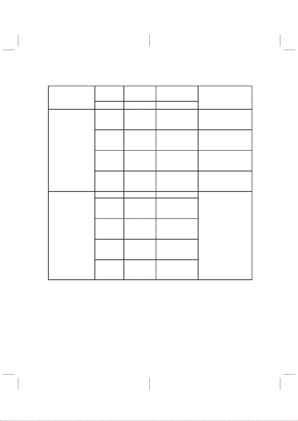
2–18
Table 2–3. Software and Hardware Requests for
Secondary Serial-Communication and Phase-Shift Truth Table
CONTROL HARDWARE
PHASE-SHIFT
WITHIN PRIMARY
OR SECONDARY
BITS TERMINALS
ADJUSTMENT
(see Section 2.15.1)
SECONDARY
REQUEST
DATA WORD
D01 D00 FC1 FC0 EARLIER LATER
(
see Note
1)
0
0
0
0
0
0
0
0
0
0
1
1
0
1
0
1
0
0
1
0
0
1
0
0
0
0
0
1
0
0
0
0
1
1
1
1
0
0
1
1
0
1
0
1
0
0
0
0
1
1
1
1
0
0
0
1
Primar
y
1
1
1
1
0
0
0
0
0
0
1
1
0
1
0
1
1
1
1
1
0
0
0
0
0
0
0
1
1
1
1
1
1
1
1
1
0
0
1
1
0
1
0
1
0
0
1
0
0
1
0
0
1
1
1
1
DS15 DS14 FC1 FC0 EARLIER LATER
0
0
0
0
0
0
0
0
0
0
1
1
0
1
0
1
0
0
0
0
0
0
0
0
Secondary
0
0
0
0
1
1
1
1
0
0
1
1
0
1
0
1
0
0
0
0
1
1
1
1
No request can be made for
secondary communication
1
1
1
1
0
0
0
0
0
0
1
1
0
1
0
1
1
1
1
1
0
0
0
0
within the secondary word.
1
1
1
1
1
1
1
1
0
0
1
1
0
1
0
1
0
0
1
0
0
1
0
0
NOTE 1: The 0 state indicates that a secondary communication is not being requested. The 1 state indicates that a
secondary communication is being requested.
2.18 Primary Serial Communications
Primary serial communications transfer the 14-bit DAC input plus two control bits (D01 and D00) to DIN of
the TLC320AC01.They simultaneously transfer the 14-bit ADC conversion result from DOUT to the
processor. The 2 LSBs are set to 0 in the ADC result.

2–19
2.18.1 Primary Serial Communications Data Format
D15 D14 D13 D12 D11 D10 D09 D08 D07 D06 D05 D04 D03 D02 D01 D00
14-bit DAC Conversion Result
2s-Complement Format
†
Control Bits
†
Since the supply voltage is single ended, the reference for 2s-complement format is ADC V
MID
. Voltages above
this reference have a 0 as the MSB, and voltages below this reference have a 1 as the MSB.
During primary serial communications, when D01 and D00 are both high in the DAC data word to DIN, a
subsequent 16 bits of control information is received by the device at DIN during a secondary
serial-communication interval. This secondary serial-communication interval begins at 1/2 the programmed
conversion time when the B register data value is even or 1/2 the programmed value minus one FCLK when
the B register data value is odd. The time between primary and secondary serial communication is
measured from the falling edge of the primary frame sync to the falling edge of the secondary frame sync
(see Section 2.19 for function and format of control words).
2.18.2 Data Format From DOUT During Primary Serial Communications
14-Bit ADC Conversion Result
2s-Complement Format
D15 is the Sign Bit
D15 D14 D13 D12 D11 D10 D09 D08 D07 D06 D05 D04 D03 D02 D01 D00
NJ
D01+0
D00+0
NJ
D01+0
D00+1
Master Mode
Slave Mode
2.19 Secondary Serial Communications
2.19.1 Data Format to DIN During Secondary Serial Communications
There are nine 16-bit configuration and control registers numbered from zero to eight. All register data
contents are represented in 2s-complement format. The general format of the commands during secondary
serial communications is as follows.
DS15 DS14 DS13 DS12 DS11 DS10 DS09 DS08 DS07 DS06 DS05 DS04 DS03 DS02 DS01 DS00
Control Bits
(2 bits)
R/W
Bit
Register Address
(5 bits)
Register Data Value
(8 bits)
All control register words are latched in the register and valid on the sixteenth falling edge of SCLK.
2.19.2 Control Data-Bit Function in Secondary Serial Communication
2.19.2.1 DS15 and DS14
In the secondary data word, bits DS15 and DS14 perform the same control function as the primary control
bits D01 and D00 do in the primary data word.
DS15 DS14 DS13 DS12 DS11 DS10 DS09 DS08 DS07 DS06 DS05 DS04 DS03 DS02 DS01 DS00
R/W
Register Address Register DataControl Bits
Hardware terminals FC1 and FC0 are valid inputs when DS15 and DS14 are both high, and they are ignored
for all other conditions.
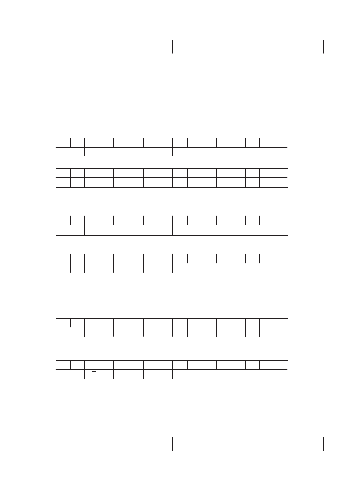
2–20
2.19.2.2 DS13 (R/W Bit)
Reset and power-up procedures set this bit to a 0, placing the device in the write mode. When this bit is set
to 1, however, the previous data content of the register being addressed is read out to the host from DOUT
as the least significant 8 bits of the 16-bit secondary word. The first 8 bits remain set to 0. Reading the data
out is nondestructive, and the contents of the register remain unchanged.
A. Write Mode (DS13 = 0)
Data In. The data word to DIN has the following general format in the write mode.
DS15 DS14 DS13 DS12 DS11 DS10 DS09 DS08 DS07 DS06 DS05 DS04 DS03 DS02 DS01 DS00
0 Register Address Register Data
Control Bits
Data Out. The shift clock shifts out all 0s as the pattern to the host from DOUT.
DS15 DS14 DS13 DS12 DS11 DS10 DS09 DS08 DS07 DS06 DS05 DS04 DS03 DS02 DS01 DS00
0000000000000000
B. Read Mode (DS13 = 1)
Data In. The data word to DIN has the following format to allow a register read. Phase shifts can
also be done in the read mode.
DS15 DS14 DS13 DS12 DS11 DS10 DS09 DS08 DS07 DS06 DS05 DS04 DS03 DS02 DS01 DS00
1 Register Address Ignored
Control Bits
Data Out. The shift clock clocks out the data of the register addressed from DOUT in the read mode in
the 8 LSBs.
DS15 DS14 DS13 DS12 DS11 DS10 DS09 DS08 DS07 DS06 DS05 DS04 DS03 DS02 DS01 DS00
00000000 Register Data
2.20 Internal Register Format
2.20.1 Pseudo-Register 0 (No-Op Address)
This address represents a no-operation command. No register I/O operation takes place, so the device can
receive secondary commands for phase adjustment without reprogramming any register. A read of the
no-op is 0. The format of the command word is as follows:
DS15 DS14 DS13 DS12 DS11 DS10 DS09 DS08 DS07 DS06 DS05 DS04 DS03 DS02 DS01 DS00
X0 0000XXXXXXXXControl Bits
2.20.2 Register 1 (A Register)
The following command loads DS07 (MSB) – DS00 into the A register.
DS15 DS14 DS13 DS12 DS11 DS10 DS09 DS08 DS07 DS06 DS05 DS04 DS03 DS02 DS01 DS00
R/W
00010 Register DataControl Bits
The data in DS07 – DS00 determines the division of the master clock to produce the internal FCLK.
FCLK frequency = MCLK/(A register contents
× 2)
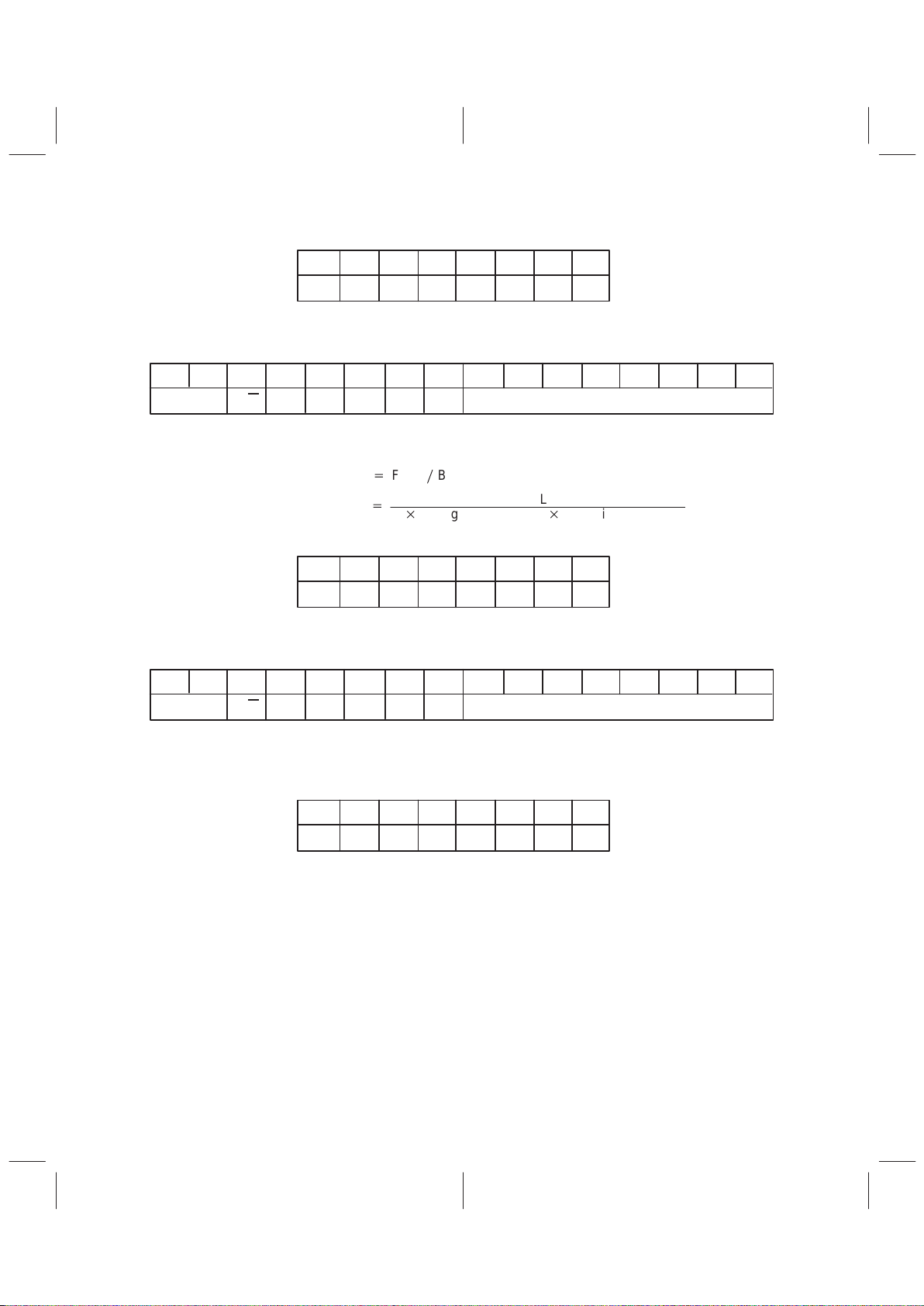
2–21
The default value of the A-register data is decimal 18 as shown below.
DS07 DS06 DS05 DS04 DS03 DS02 DS01 DS00
00101000
2.20.3 Register 2 (B Register)
The following command loads DS07 (MSB) – DS00 into the B register.
DS15 DS14 DS13 DS12 DS11 DS10 DS09 DS08 DS07 DS06 DS05 DS04 DS03 DS02 DS01 DS00
R/W
01000 Register DataControl Bits
The data in DS07 – DS00 controls the division of FCLK to generate the conversion clock as given in
equation 20:
Conversion frequency
+
FCLKń(B register contents)
+
MCLK
2 Are
g
ister contents Bregister contents
(20)
The default value of the B-register data is decimal 18 as shown below.
DS07 DS06 DS05 DS04 DS03 DS02 DS01 DS00
00101000
2.20.4 Register 3 (A′ Register)
The following command contains the A′-register address and loads DS07(MSB) – DS00 into the A′ register.
DS15 DS14 DS13 DS12 DS11 DS10 DS09 DS08 DS07 DS06 DS05 DS04 DS03 DS02 DS01 DS00
R/W
01010 Register DataControl Bits
The data in DS07 – DS00 is in 2s-complement format and controls the number of master-clock periods that
the sampling time is shifted.
The default value of the A
′-register data is 0 as shown below.
DS07 DS06 DS05 DS04 DS03 DS02 DS01 DS00
00000000

2–22
2.20.5 Register 4 (Amplifier Gain-Select Register)
The following command contains the amplifier gain-select register address with selection code for the
monitor output (DS05–DS04), analog input (DS03–DS02), and analog output (DS01–DS00)
programmable gains.
DS15 DS14 DS13 DS12 DS11 DS10 DS09 DS08 DS07 DS06 DS05 DS04 DS03 DS02 DS01 DS00
R/W
00001Control Bits XX
**** **
Monitor output gain = squelch
Monitor output gain = 0 dB
Monitor output gain = –8 dB
Monitor output gain = –18 dB
0
0
1
1
0
1
0
1
0
0
1
1
0
1
0
1
0
0
1
1
0
1
0
1
Analog input gain = squelch
Analog input gain = 0 dB
Analog input gain = 6 dB
Analog input gain = 12 dB
Analog output gain = squelch
Analog output gain = 0 dB
Analog output gain = –6 dB
Analog output gain = –12 dB
The default value of the monitor output gain is squelch, which corresponds to data bits DS05 and DS04 equal
to 00 (binary).
The default value of the analog input gain is 0 dB, which corresponds to data bits DS03 and DS02 equal
to 01 (binary).
The default value of the analog output gain is 0 dB, which corresponds to data bits DS01 and DS00 equal
to 01 (binary).
The default data value is shown below.
DS07 DS06 DS05 DS04 DS03 DS02 DS01 DS00
00000011
2.20.6 Register 5 (Analog Configuration Register)
The following command loads the analog configuration register with the individual bit functions described
below.
DS15 DS14 DS13 DS12 DS11 DS10 DS09 DS08 DS07 DS06 DS05 DS04 DS03 DS02 DS01 DS00
R/W
00011Control Bits XX
X
** **
Must be set to 0 0
High-pass filter disabled
High-pass filter enabled
Enable analog input summing
X
1
Analog loopback enabled 00
Enables IN+ and IN– (disables AUXIN+ and AUXIN–) 0 1
Enables AUXIN+ and AUXIN– (disables IN+ and IN–)
10
11
0
The default value of the high-pass-filter enable bit is 0, which places the high-pass filter in the signal path.
The default values of DS01 and DS00 are 0 and 1 which enables IN+ and IN–.

2–23
The power-up and reset conditions are as shown below.
DS03 DS02 DS01 DS00
0010
In the read mode, eight bits are read but the 4 LSBs are repeated as the 4 MSBs.
2.20.7 Register 6 (Digital Configuration Register)
The following command loads the digital configuration register with the individual bit functions described
below.
DS15 DS14 DS13 DS12 DS11 DS10 DS09 DS08 DS07 DS06 DS05 DS04 DS03 DS02 DS01 DS00
R/W
01001Control Bits XX
** **
ADC and DAC conversion free run
Inactive
1
0
FSD output disable
Enable
1
0
16-Bit mode, ignore primary LSBs
Normal operation
1
0
Software reset
(upon reset, this bit is automatically reset to 0)
Inactive reset
1
Software power-down active (automatically reset to 0
after PWR
DWN is cycled high to low and back to high)
1
0
**
Force secondary communications
Normal operation
1
0
0
Power-down function external
(uses PWR DWN)
The default value of DS07–DS00 is 0 as shown below.
DS07 DS06 DS05 DS04 DS03 DS02 DS01 DS00
00000000
2.20.8 Register 7 (Frame-Sync Delay Register)
The following command contains the frame-sync delay (FSD) register address and loads DS07
(MSB) –DS00 into the FSD register. The data byte (DS01 –DS00) determines the number of SCLKs
between FS
and the delayed frame-sync signal, FSD. The minimum data value for this register is
decimal 18.
DS15 DS14 DS13 DS12 DS11 DS10 DS09 DS08 DS07 DS06 DS05 DS04 DS03 DS02 DS01 DS00
R/W
01011 Register DataControl Bits
The default value of DS07 – DS00 is 0 as shown below.
DS07 DS06 DS05 DS04 DS03 DS02 DS01 DS00
00000000
When using a slave device, register 7 must be the last register programmed.

2–24
2.20.9 Register 8 (Frame-Sync Number Register)
The following command contains the frame-sync number (FSN) register address and loads DS07
(MSB)–DS00 into the FSN register. The data byte determines the number of frame-sync signals generated
by the TLC320AC01. This number is equal to the number of slaves plus one.
DS15 DS14 DS13 DS12 DS11 DS10 DS09 DS08 DS07 DS06 DS05 DS04 DS03 DS02 DS01 DS00
R/W
00100 Register DataControl Bits
The default value of DS07–DS00 is 1 as shown below.
DS07 DS06 DS05 DS04 DS03 DS02 DS01 DS00
00000010

3–1
3 Specifications
3.1 Absolute Maximum Ratings Over Operating Free-Air Temperature Range
(Unless Otherwise Noted)
†
Supply voltage range, DGTL V
DD
(see Notes 1 and 2) –0.3 V to 6.5 V. . . . . . . . . . . . . . .
Supply voltage range, DAC V
DD
(see Notes 1 and 2) –0.3 V to 6.5 V. . . . . . . . . . . . . . . .
Supply voltage range, ADC V
DD
(see Notes 1 and 2) –0.3 V to 6.5 V. . . . . . . . . . . . . . . .
Differential supply voltage range, DGTL V
DD
to DAC VDD –0.3 V to 6.5 V. . . . . . . . . . . .
Differential supply voltage range, all positive supply voltages to
ADC GND, DAC GND, DGTL GND, SUBS –0.3 V to 6.5 V. . . . . . . . . . . . . . . . . . . .
Output voltage range, DOUT –0.3 V to DGTL V
DD
+ 0.3 V. . . . . . . . . . . . . . . . . . . . . . . . .
Input voltage range, DIN –0.3 V to DGTL V
DD
+ 0.3 V. . . . . . . . . . . . . . . . . . . . . . . . . . . . .
Ground voltage range, ADC GND, DAC GND,
DGTL GND, SUBS –0.3 V to DGTL V
DD
+ 0.3 V. . . . . . . . . . . . . . . . . . . . . . . . . . . .
Operating free-air temperature range, T
A
0°C to 70°C. . . . . . . . . . . . . . . . . . . . . . . . . . . .
Storage temperature range, T
stg
–40°C to 125°C. . . . . . . . . . . . . . . . . . . . . . . . . . . . . . . . .
Lead temperature 1,6 mm (1/16 inch) from case for 10 seconds 260°C. . . . . . . . . . . . . .
†
Stresses beyond those listed under “absolute maximum ratings” may cause permanent damage to the device. These
are stress ratings only, and functional operation of the device at these or any other conditions beyond those indicated
under “recommended operating conditions” is not implied. Exposure to absolute-maximum-rated conditions for
extended periods may affect device reliability.
3.2 Recommended Operating Conditions (see Note 2)
MIN NOM MAX UNIT
V
DD
Positive supply voltage 4.5 5 5.5 V
Steady-state differential voltage between any two supplies 0.1 V
V
IH
High-level digital input voltage 2.2 V
V
IL
Low-level digital input voltage 0.8 V
I
O
Load output current from ADC V
MID
and DAC 100 µA
Conversion time for the ADC and DAC channels 10 FCLK periods
f
MCLK
Master-clock frequency 10.368 15 MHz
V
ID(PP)
Analog input voltage (differential, peak to peak) 6 V
Differential output load resistance 600
R
L
Single-ended to buffered DAC V
MID
voltage load resistance 300
Ω
T
A
Operating free-air temperature 0 70 °C
NOTES: 1. Voltage values for DGTL VDD are with respect to DGTL GND, voltage values for DAC VDD are with respect
to DAC GND, and voltage values for ADC VDD are with respect to ADC GND. For the subsequent electrical,
operating, and timing specifications, the symbol VDD denotes all positive supplies. DAC GND, ADC GND,
DGTL GND, and SUBS are at 0 V unless otherwise specified.
2. To avoid possible damage to these CMOS devices and associated operating parameters, the sequence
below should be followed when applying power:
(1) Connect SUBS, DGTL GND, ADC GND, and DAC GND to ground.
(2) Connect voltages ADC VDD,and DAC VDD.
(3) Connect voltage DGTL VDD.
(4) Connect the input signals.
When removing power, follow the steps above in reverse order.
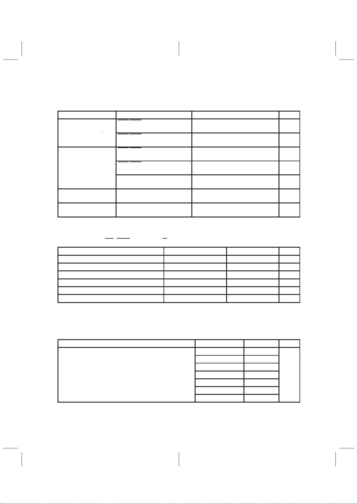
3–2
3.3 Electrical Characteristics Over Recommended Range of Operating
Free-Air Temperature, MCLK = 5.184 MHz, V
DD
= 5 V, Outputs
Unloaded, Total Device
PARAMETER TEST CONDITIONS MIN TYP
†
MAX UNIT
Supply
PWR DWN = 1 and clock signals
present
20 25 mA
I
DD
y
current
PWR
DWN = 0 after 500 µs and
clock signals present
1 2 mA
PWR DWN = 1 and clock signals
present
100 mW
P
D
Power
dissipation
PWR
DWN = 0 after 500 µs and
clock signals present
5 mW
Software power down, (bit D00,
register 6 set to 1)
15 20 mW
ADC V
MID
Midpoint
voltage
No load
ADC VDD/2
–0.1
ADC VDD/2
+0.1
V
DAC V
MID
Midpoint
voltage
No load
DAC VDD/2
–0.1
DAC VDD/2
+0.1
V
3.4 Electrical Characteristics Over Recommended Range of Operating
Free-Air Temperature, V
DD
= 5 V, Digital I/O Terminals (DIN, DOUT, EOC,
FC0, FC1, FS
, FSD, MCLK, M/S, SCLK)
PARAMETER TEST CONDITIONS MIN TYP†MAX UNIT
V
OH
High-level output voltage IOH = –1.6 mA 2.4 V
V
OL
Low-level output voltage IOL = 1.6 mA 0.4 V
I
IH
High-level input current, any digital input VI = 2.2 V to DGTL V
DD
10 µA
I
IL
Low-level input current, any digital input VI = 0 V to 0.8 V 10 µA
C
i
Input capacitance 5 pF
C
o
Output capacitance 5 pF
†
All typical values are at VDD = 5 V and TA = 25°C.
3.5 Electrical Characteristics Over Recommended Range of Operating
Free-Air Temperature, V
DD
= 5 V, ADC and DAC Channels
3.5.1 ADC Channel Filter Transfer Function, FCLK = 144 kHz, fs = 8 kHz
PARAMETER TEST CONDITIONS MIN MAX UNIT
fi = 50 Hz –2
fi = 200 Hz –1.8 –0.15
fi = 300 Hz to 3 kHz –0.15 0.15
Gain relative to gain at fi = 1020 Hz (see Note 3)
fi = 3.3 kHz –0.35 0.03
dB
fi = 3.4 kHz –1 –0.1
fi = 4 kHz –14
fi ≥ 4.6 kHz –32
NOTE 3: The differential analog input signals are sine waves at 6 V peak to peak. The reference gain is at 1020 Hz.

3–3
3.5.2 ADC Channel Input, VDD = 5 V, Input Amplifier Gain = 0 dB (Unless Otherwise
Noted)
PARAMETER TEST CONDITIONS MIN TYP†MAX UNIT
p
p
Single-ended 3 V
V
I(PP)
Peak-to-peak input voltage (see Note 4)
Differential 6 V
ADC converter offset error Band-pass filter selected 10 30 mV
CMRR
Common-mode rejection ratio at IN+, IN–,
AUX IN+, AUX IN– (see Note 5)
55 dB
r
i
Input resistance at IN+, IN–, AUX IN+,
AUX IN–
100 kΩ
Squelch
DS03, DS02 = 0 in
register 4
60 dB
†
All typical values are at VDD = 5 V and TA = 25°C.
NOTES: 4. The differential range corresponds to the full-scale digital output.
5. Common-mode rejection ratio is the ratio of the ADC converter offset error with no signal and the ADC
converter offset error with a common-mode nonzero signal applied to either IN + and IN – together or
AUX IN+ and AUX IN– together.
3.5.3 ADC Channel Signal-to-Distortion Ratio, VDD = 5 V, fs = 8 kHz (Unless
Otherwise Noted)
AV = 0 dB AV = 6 dB AV = 12 dB
PARAMETER
TEST CONDITIONS
MIN MAX MIN MAX MIN MAX
UNIT
VI = –6 dB to –1 dB 68 — —
VI = –12 dB to –6 dB 63 68 —
VI = –18 dB to –12 dB 56 63 68
ADC channel signal-to-
VI = –24 dB to –18 dB 51 57 63
distortion ratio
(
see Note 6
)
VI = –30 dB to –24 dB 43 51 57
dB
(see Note 6)
VI = –36 dB to –30 dB 39 45 51
VI = –42 dB to –36 dB 33 39 45
VI = –48 dB to –42 dB 27 32 39
NOTE 6: The analog-input test signal is a 1020-Hz sine wave with 0 dB = 6 V peak to peak as the reference level for
the analog-input signal.
3.5.4 DAC Channel Filter Transfer Function, FCLK = 144 kHz, fs = 9.6 kHz, VDD = 5 V
PARAMETER TEST CONDITIONS MIN MAX UNIT
fi < 200 Hz 0.15
fi = 200 Hz –0.5 0.15
fi = 300 Hz to 3 kHz –0.15 0.15
Gain relative to gain at fi = 1020 Hz (see Note 7)
fi = 3.3 kHz –0.35 0.03
dB
fi = 3.4 kHz –1 –0.1
fi = 4 kHz –14
fi ≥ 4.6 kHz –32
NOTE 7: The input signal is the digital equivalent of a 1020-Hz sine wave (digital full scale = 0 dB). The nominal
differential DAC channel output with this input condition is 6 V peak to peak.
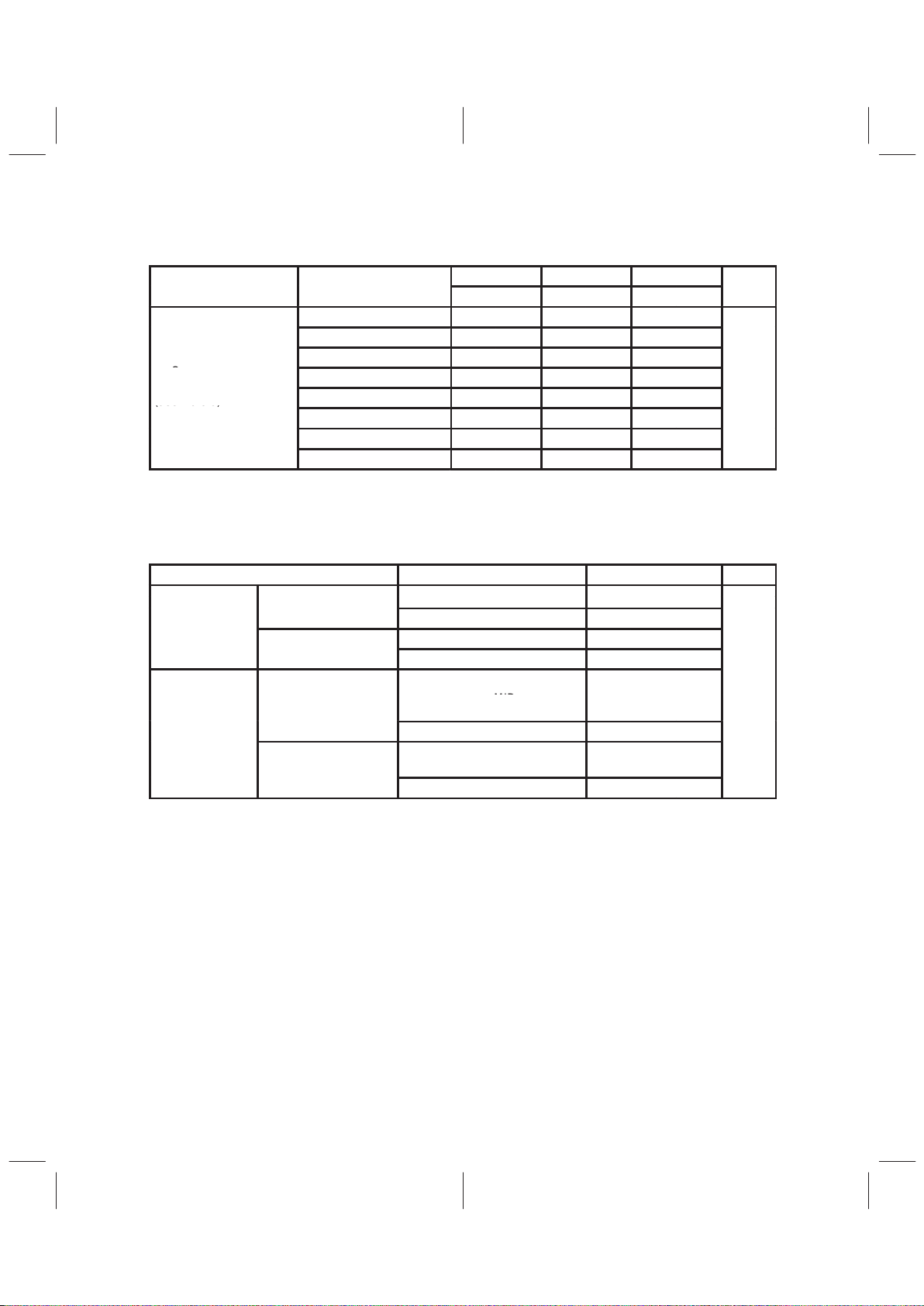
3–4
3.5.5 DAC Channel Signal-to-Distortion Ratio, VDD = 5 V, fs = 8 kHz (Unless
Otherwise Noted)
AV = 0 dB AV = –6 dB AV = –12 dB
PARAMETER
TEST CONDITIONS
MIN MAX MIN MAX MIN MAX
UNIT
VO = –6 dB to 0 dB 68 — —
VO = –12 dB to –6 dB 63 68 —
VO = –18 dB to –12 dB 57 63 68
DAC channel signal-to-
VO = –24 dB to –18 dB 51 57 63
distortion ratio
(
see Note 8
)
VO = –30 dB to –24 dB 45 51 57
dB
(see Note 8)
VO = –36 dB to –30 dB 39 45 51
VO = –42 dB to –36 dB 33 39 48
VO = –48 dB to –42 dB 27 33 39
NOTE 8: The input signal, VI, is the digital equivalent of a 1020-Hz sine wave (full-scale analog output at full-scale digital
input = 0 dB). The nominal differential DAC channel output with this input condition is 6 V peak to peak. The
load impedance for the DAC output buffer is 600 Ω from OUT+ to OUT –.
3.5.6 System Distortion, VDD = 5 V, fs = 8 kHz, FCLK = 144 kHz (Unless Otherwise
Noted)
PARAMETER TEST CONDITIONS MIN TYP†MAX UNIT
p
Single-ended input (see Note 9)
82
ADC channel
Second harmonic
Differential input (see Note 9) 70 82
attenuation
Third harmonic and
Single-ended input (see Note 9) 77
higher harmonics
Differential input (see Note 9) 70 77
Single-ended output
Second harmonic
(buff
ered
DAC V
MID
)
(see Note 10)
82
dB
DAC channel
Differential output (see Note 10) 70 82
attenuation
Third harmonic and
Single-ended output
(see Note 10)
77
higher harmonics
Differential output (see Note 10) 70 77
†
All typical values are at VDD = 5 V and TA = 25°C.
NOTES: 9. The input signal is a 1020-Hz sine wave for the ADC channel. Harmonic distortion is defined for an input
level of –1 dB.
10. The input signal is the digital equivalent of a 1020-Hz sine wave (digital full scale = 0 dB). The nominal
differential DAC channel output with this input condition is 6 V peak to peak. The load impedance for the
DAC output buffer is 600 Ω from OUT+ to OUT–. Harmonic distortion is specified for a signal input level
of 0 dB.

3–5
3.5.7 Noise, Low-Pass and Band-Pass Switched-Capacitor Filters Included,
V
DD
= 5 V (Unless Otherwise Noted)
PARAMETER TEST CONDITIONS MIN TYP†MAX UNIT
Inputs tied to ADC V
MID
,
ADC idle-channel noise
f
s
=
8 kH
z,
FCLK
=
144 kH
z,
(see Note 11)
180
300
Broad-band noise
DIN INPUT = 00000000000000
,
180 300
µVrms
DAC idl
e-channe
l
Noise (0 to 7.2 kHz)
DIN INPUT 00000000000000,
fs = 8 kHz, FCLK = 144 kHz,
180 300
noise
Noise (0 to 3.6 kHz)
(see Note 12)
180 300
†
All typical values are at VDD = 5 V and TA = 25°C.
NOTES: 11. The ADC channel noise is calculated by taking the RMS value of the digital output codes of the ADC
channel and converting to microvolts.
12. The DAC channel noise is measured differentially from OUT+ to OUT– across 600 Ω.
3.5.8 Absolute Gain Error, VDD = 5 V, fs = 8 kHz (Unless Otherwise Noted)
PARAMETER TEST CONDITIONS MIN MAX UNIT
p
TA = 25°C ±0.5
ADC channel absolute gain error (see Note 13)
–1-dB
input signal
TA = 0 – 70°C ±1
0-dB input signal,
TA = 25°C ±0.5
dB
DAC channel absolute gain error (see Note 14)
g
RL = 600 Ω
TA = 0 – 70°C ±1
NOTES: 13. ADC absolute gain error is the variation in gain from the ideal gain over the specified input signal levels.
The gain is measured with a –1-dB, 1020-Hz sine wave. The –1-dB input signal allows for any positive gain
or offset error that may affect gain measurements at or close to 0-dB input signal levels.
14. The DAC input signal is the digital equivalent of a 1020-Hz sine wave (full-scale analog output at digital fullscale input = 0 dB). The nominal differential DAC channel output voltage with this input condition is 6 V peak
to peak. The load impedance for the DAC output buffer is 600 Ω from OUT+ to OUT–.
3.5.9 Relative Gain and Dynamic Range, VDD = 5 V, fs = 8 kHz (Unless Otherwise
Noted)
PARAMETER TEST CONDITIONS MIN MAX UNIT
ADC channel relative gain tracking error
(see Note 15)
–48-dB to –1-dB input signal range ±0.15
DAC channel relative gain tracking error
(see Note 16)
–48-dB to 0-dB input signal range
R
L(diff)
= 600 Ω
±0.15
dB
NOTES: 15. ADC gain tracking is the ratio of the measured gain at one ADC channel input level to the gain measured
at any other input level. The ADC channel input is a –1-dB 1020-Hz sine wave input signal. A –1-dB input
signal allows for any positive gain or offset error that may affect gain measurements at or close to 0-dB ADC
input signal levels.
16. DAC gain tracking is the ratio of the measured gain at one DAC channel digital input level to the gain
measured at any other input level. The DAC-channel input signal is the digital equivalent of a 1020-Hz sine
wave (digital full scale = 0 dB). The nominal differential DAC channel output voltage with this input condition
is 6 V peak to peak. The load impedance for the DAC output buffer is 600 Ω from OUT+ to OUT–.

3–6
3.5.10 Power-Supply Rejection, VDD = 5 V (Unless Otherwise Noted) (see Note 17)
PARAMETER TEST CONDITIONS MIN TYP†MAX UNIT
pp
fi = 0 to 30 kHz 50
ADC V
DD
Suppl
y-v
oltage rejection ratio, ADC channel
fi = 30 to 50 kHz 55
pp
fi = 0 to 30 kHz 40
DAC V
DD
Suppl
y-v
oltage rejection ratio, DAC channel
fi = 30 to 50 kHz 45
pp
fi = 0 to 30 kHz 50
DGTL VDDSuppl
y-v
oltage rejection ratio, ADC channel
fi = 30 to 50 kHz 55
Single ended,
fi = 0 to 30 kHz
40
dB
pp
fi = 30 to 50 kHz 45
DGTL VDDSuppl
y-v
oltage rejection ratio, DAC channel
Differential,
fi = 0 to 30 kHz
40
fi = 30 to 50 kHz 45
†
All typical values are at VDD = 5 V and TA = 25°C.
NOTE 17: Power supply rejection measurements are made with both the ADC and the DAC channels idle and a 200-mV
peak-to-peak signal applied to the appropriate supply .
3.5.11 Crosstalk Attenuation, VDD = 5 V (Unless Otherwise Noted)
PARAMETER TEST CONDITIONS MIN TYP†MAX UNIT
ADC channel crosstalk attenuation
DAC channel idle with
DIN = 00000000000000,
ADC input = 0 dB,
1020-Hz sine wave,
Gain = 0 dB (see Note 18)
80 dB
ADC channel idle with INP, INM,
AUX IN+, and AUX IN– at ADC V
MID
80
DAC channel crosstalk attenuation
DAC channel input = digital equivalent
of a 1020-Hz sine wave (see Note 19)
80
dB
†
All typical values are at VDD = 5 V and TA = 25°C.
NOTES: 18. The test signal is a 1020-Hz sine wave with a 0 dB = 6-V peak-to-peak reference level for the analog input
signal.
19. The input signal is the digital equivalent of a 1020-Hz sine wave (digital full scale = 0 dB). The nominal
differential DAC channel output with this input condition is 6 V peak to peak. The load impedance for the
DAC output buffer is 600 Ω from OUT+ to OUT–.
3–7
3.5.12 Monitor Output Characteristics, VDD = 5 V (Unless Otherwise Noted)
(see Note 20)
PARAMETER TEST CONDITIONS MIN TYP
†
MAX UNIT
V
O(PP)
Peak-to-peak ac output
voltage
Quiescent level = ADC V
MID
ZL = 10 kΩ and 60 pF
1.3 1.5 V
V
OO
Output offset voltage
No load, single ended
relative to ADC V
MID
5 10 mV
V
OC
Output common-mode voltage No load
0.4 ADC
V
DD
0.5 ADC
V
DD
0.6 ADC
V
DD
V
r
o
DC output resistance 50 Ω
Gain = 0 dB –0.2 0 0.2
Gain 2 = –8 dB –8.2 –8 –7.8
AVVoltage gain (see Note 21)
Gain 3 = –18 dB –18.4 –18 –17.6
dB
Squelch (see Note 22) –60
†
All typical values are at VDD = 5 V and TA = 25°C.
NOTES: 20. All monitor output tests are performed with a 10-kΩ load resistance.
21. Monitor gains are measured with a 1020-Hz, 6-V peak-to-peak sine wave applied differentially between
IN+ and IN–.The monitor output gains are nominally 0 dB, –8 dB, and –18 dB relative to its input; however,
the output gains are –6 dB relative to IN+ and IN– or AUX IN+ and AUX IN–.
22. Squelch is measured differentially with respect to ADC V
MID
.
3–8
3.6 Timing Requirements and Specifications in Master Mode
3.6.1 Recommended Input Timing Requirements for Master Mode, VDD = 5 V
MIN NOM MAX UNIT
t
r(MCLK)
Master clock rise time 5 ns
t
f(MCLK)
Master clock fall time 5 ns
Master clock duty cycle 40% 60%
t
w(RESET)
RESET pulse duration 1 MCLK
t
su(DIN)
DIN setup time before SCLK low (see Figure 4–2) 25 ns
t
h(DIN)
DIN hold time after SCLK low (see Figure 4–2) 20 ns
3.6.2 Operating Characteristics Over Recommended Range of Operating Free-Air
T emperature, V
DD
= 5 V (Unless Otherwise Noted) (see Note 23)
PARAMETER MIN TYP†MAX UNIT
t
f(SCLK)
Shift clock fall time (see Figure 4–2) 13 18 ns
t
r(SCLK)
Shift clock rise time (see Figure 4–2) 13 18 ns
Shift clock duty cycle 45% 55%
t
d(CH-FL)
Delay time from SCLK high to FSD low
(see Figures 4–2 and 4–4 and Note 24)
5 15 ns
t
d(CH-FH)
Delay time from SCLK high to FS high (see Figure 4–2) 5 20 ns
t
d(CH-DOUT)
Delay time from SCLK high to DOUT valid
(see Figures 4–2 and 4–7)
20 ns
t
d(CH-DOUTZ)
Delay time from SCLK↑ to DOUT in high-impedance state
(see Figure 4–8)
20 ns
t
d(ML-EL)
Delay time from MCLK low to EOC low (see Figure 4–9) 40 ns
t
d(ML-EH)
Delay time from MCLK low to EOC high (see Figure 4–9) 40 ns
t
f(EL)
EOC fall time (see Figure 4–9) 13 ns
t
r(EH)
EOC rise time (see Figure 4–9) 13 ns
t
d(MH-CH)
Delay time from MCLK high to SCLK high 50 ns
t
d(MH-CL)
Delay time from MCLK high to SCLK low 50 ns
†
All typical values are at VDD = 5 V and TA = 25°C.
NOTES: 23. All timing specifications are valid with CL = 20 pF.
24. FSD
occurs 1/2 shift-clock cycle ahead of FS when the device is operating in the master mode.
3–9
3.7 Timing Requirements and Specifications in Slave Mode and Codec
Emulation Mode
3.7.1 Recommended Input Timing Requirements for Slave Mode, VDD = 5 V
MIN NOM MAX UNIT
t
r(MCLK)
Master clock rise time 5 ns
t
f(MCLK)
Master clock fall time 5 ns
Master clock duty cycle 40% 60%
t
w(RESET)
RESET pulse duration 1 MCLK
t
su(DIN)
DIN setup time before SCLK low (see Figure 4–3) 20 ns
t
h(DIN)
DIN hold time after SCLK high (see Figure 4–3) 20 ns
t
su(FL-CH)
Setup time from FS low to SCLK high ±SCLK/4 ns
3.7.2 Operating Characteristics Over Recommended Range of Operating Free-Air
T emperature, V
DD
= 5 V (Unless Otherwise Noted) (see Note 23)
PARAMETER MIN TYP†MAX UNIT
t
c(SCLK)
Shift clock cycle time (see Figure 4–3) 125 ns
t
f(SCLK)
Shift clock fall time (see Figure 4–3) 18 ns
t
r(SCLK)
Shift clock rise time (see Figure 4–3) 18 ns
Shift clock duty cycle 45% 55%
t
d(CH-FDL)
Delay time from SCLK high to FSD low (see Figure 4–6) 50 ns
t
d(CH-FDH)
Delay time from SCLK high to FSD high 40 ns
t
d(FL-FDL)
Delay time from FS low to FSD low (slave to slave)
(see Figure 4–5)
40 ns
t
d(CH-DOUT)
Delay time from SCLK high to DOUT valid
(see Figures 4–3 and 4–7)
40 ns
t
d(CH-DOUTZ)
Delay time from SCLK↑ to DOUT in high-impedance state
(see Figure 4–8)
20 ns
t
d(ML-EL)
Delay time from MCLK low to EOC low (see Figure 4–9) 40 ns
t
d(ML-EH)
Delay time from MCLK low to EOC high (see Figure 4–9) 40 ns
t
f(EL)
EOC fall time (see Figure 4–9) 13 ns
t
r(EH)
EOC rise time (see Figure 4–9) 13 ns
t
d(MH-CH)
Delay time from MCLK high to SCLK high 50 ns
t
d(MH-CL)
Delay time from MCLK high to SCLK low 50 ns
†
All typical values are at VDD = 5 V and TA = 25°C.
NOTE 23: All timing specifications are valid with CL = 20 pF.

3–10

4–1
4 Parameter Measurement Information
_
+
IN+ or AUX IN+
IN– or AUX IN–
To Multiplexer
R
fb
R
fb
_
+
Rfb = R for DS03 = 0 and DS02 = 1
Rfb = 2R for DS03 = 1 and DS02 = 0
Rfb = 4R for DS03 = 1 and DS02 = 1
R = 100 kΩ nominal
R
R
Figure 4–1. IN+ and IN– Gain-Control Circuitry
Table 4–1. Gain Control (Analog Input Signal Required for
Full-Scale Bipolar A/D-Conversion 2s Complement)
†
CONTROL REGISTER 4
A/D CONVERSION
INPUT CONFIGURATION
DS03 DS02
ANALOG INPUT
‡
RESULT
0 0 All Squelch
Differential configuration
p
0 1 VID = ±3 V ±Full scale
Analog input= IN
+ – IN–
= AUX IN+ – AUX IN–
1 0 VID = ±1.5 V ±Full scale
AUX IN+ AUX IN
1 1 VID = ±0.75 V ±Full scale
0 0 All Squelch
Single-ended configuration
§
0 1 VI = ±1.5 V ±Half scale
Anal
og input= IN+ –
V
MID
= AUX IN+ – V
1 0 VI = ±1.5 V ±Full scale
= AUX IN+ V
MID
1 1 VI = ±0.75 V ±Full scale
†
VDD = 5 V
‡
VID = differential input voltage, VI = input voltage referenced to ADC V
MID
with IN – or AUX IN – connected to
ADC V
MID
. In order to minimize distortion, it is recommended that the analog input not exceed 0.1 dB below full scale.
§
For single-ended inputs, the analog input voltage should not exceed the supply rails. All single-ended inputs should be
referenced to the internal reference voltage, ADC V
MID
, for best common-mode performance.
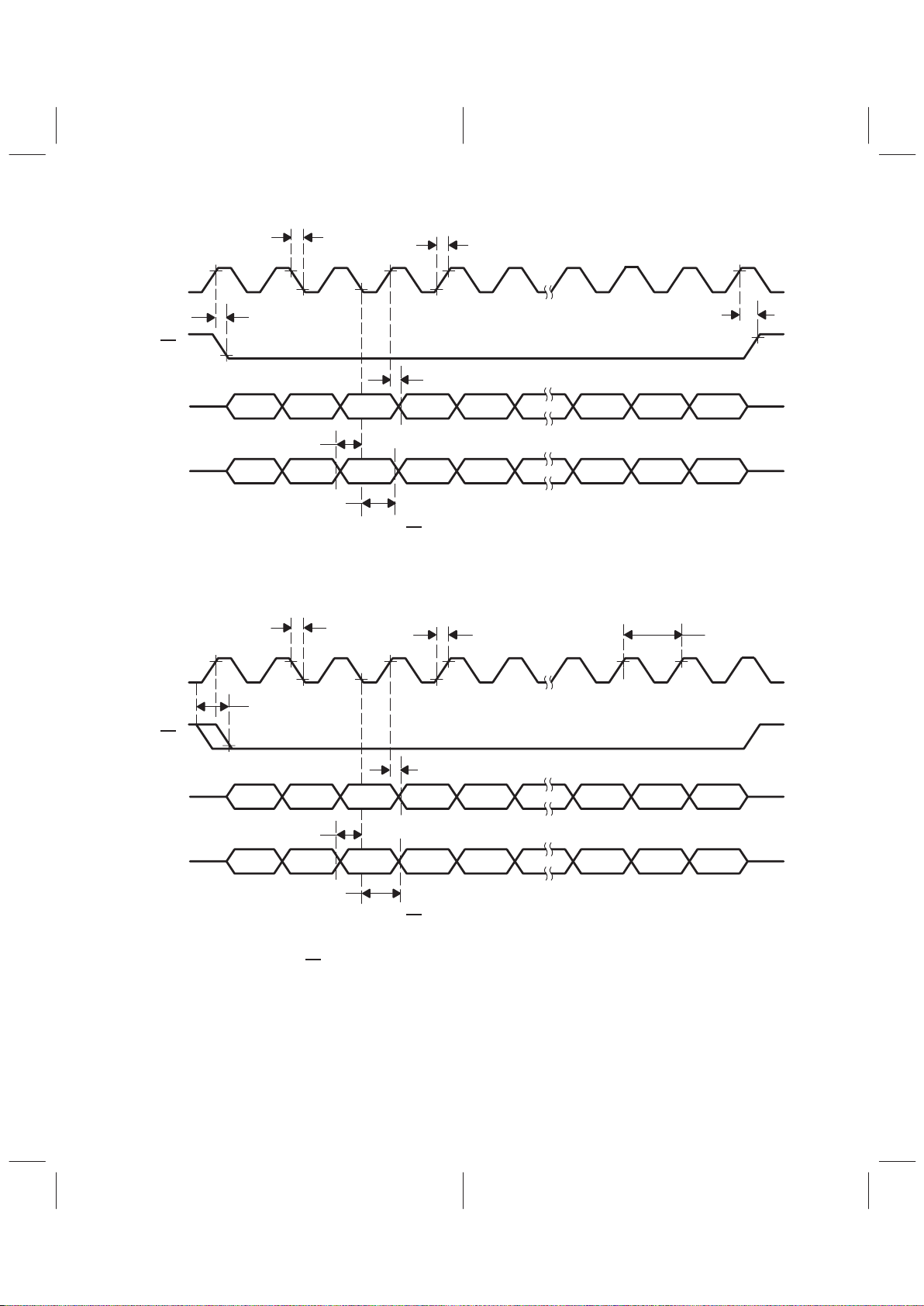
4–2
D15 D14 D13 D12 D11 D2 D1 D0
t
f(SCLK)
0.8 V
SCLK
FS
†
t
r(SCLK)
t
d(CH-FH)
t
d(CH-FL)
0.8 V
2 V 2 V
t
d(CH-DOUT)
D15 D14 D13 D12 D11 D2 D1 D0
t
su(DIN)
t
h(DIN)
DOUT
‡
DIN
2 V
2 V
†
The time between falling edges of two primary FS signals is the conversion period.
‡
The data on DOUT are shifted out on the rising edge of the shift clock, and the data on DIN are shifted in on the falling
edge of the shift clock.
Figure 4–2. AIC Stand-Alone and Master-Mode Timing
D15 D14 D13 D12 D1 1 D2 D1 D0
2 V 2 V
t
f(SCLK)
0.8 V
SCLK
FS
†
t
r(SCLK)
t
c(SCLK)
§
2 V 2 V
t
d(CH-DOUT)
D15 D14 D13 D12 D1 1 D2 D1 D0
t
su(DIN)
t
h(DIN)
DOUT
‡
DIN
†
The time between falling edges of two primary FS signals is the conversion period.
‡
The data on DOUT are shifted out on the rising edge of the shift clock, and the data on DIN are shifted in on the falling
edge of the shift clock.
§
The high-to-low transition of FS
must must occur within ±1/4 of a shift-clock period around the 2-V level of the shift clock
for the codec mode.
Figure 4–3. AIC Slave and Codec Emulation Mode

4–3
t
d(CH-FL)
2.4 V
0.8 V
SCLK
0.8 V
FS
FSD
SCLK Period/2
NOTE A: Timing shown is for the TLC320AC01 operating as the master or as a stand-alone device.
Figure 4–4. Master or Stand-Alone FS and FSD Timing
t
d(FL-FDL)
0.8 V
0.8 V
FSD
FS
NOTE A: Timing shown is for the TLC320AC01 operating in the slave mode (FS and SCLK signals are generated
externally). The programmed data value in the FSD register is 0.
Figure 4–5. Slave FS to FSD Timing
t
d(CH-FDL)
0.8 V
2.4 V
0.8 V
SCLK
FSD
NOTE A: Timing shown is for the TLC320AC01 operating in the slave mode (FS and SCLK signals are generated
externally). There is a data value in the FSD register greater than 18 (decimal).
Figure 4 – 6. Slave SCLK to FSD Timing
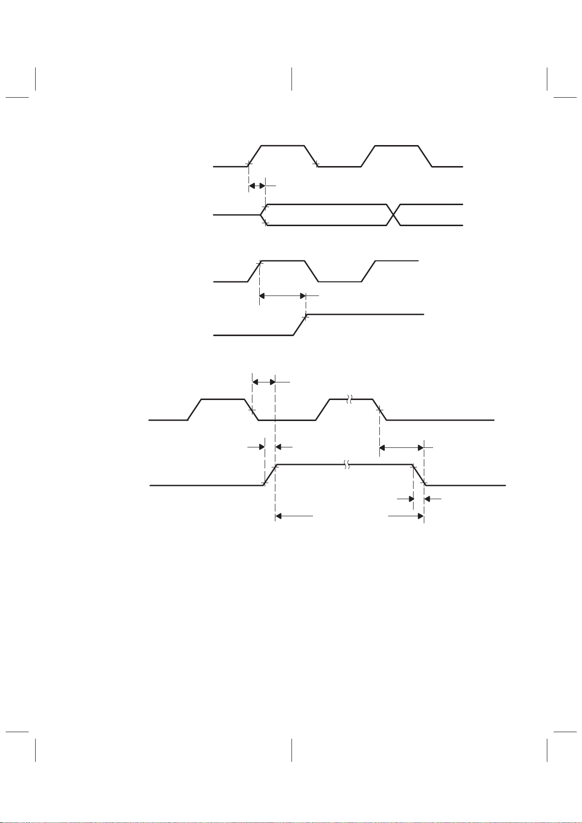
4–4
0.8 V
2 V
SCLK
0.4 V
DOUT
2.4 V
0.4 V
2.4 VHi-Z
t
d(CH-DOUT)
Figure 4–7. DOUT Enable Timing From Hi-Z
0.8 V
2 V
0.8 V
SCLK
t
d(CH-DOUTZ)
Hi-Z
DOUT
Figure 4–8. DOUT Delay Timing to Hi-Z
2 V
2.4 V
MCLK
t
r(EH)
EOC
t
d(ML-EH)
Internal ADC
Conversion Time
t
f(EL)
t
d(ML-EL)
0.8 V
0.4 V 0.4 V
2.4 V
2 V
0.8 V
Figure 4–9. EOC Frame Timing

4–5
Delay Is m Shift Clocks
†
Delay Is m Shift Clocks
†
Delay Is m Shift Clocks
†
Master
FS
Master FSD,
Slave Device 1 FS
Slave Device 1 FSD,
Slave Device 2 FS
Slave Device 2 FSD,
Slave Device 3 FS
Slave Device
(n – 1) FSD
,
Slave Device n FS
†
The delay time from any FS signals to the corresponding FSD signals is m shift clocks with the value of m being the
numerical value of the data programmed into the FSD register. In the master mode with slaves, the same data word
programs the master and all slave devices; therefore, master to slave 1, slave 1 to slave 2, slave 2 to slave 3, etc., have
the same delay time.
Figure 4–10. Master-Slave Frame-Sync Timing After a Delay Has Been
Programmed Into the FSD Registers
1/2 Period
Sampling
Period
FSD
Value
MP MP MP
MP MP MPMS MS
MP MP MPSP SP
MP MP MPMS SP SPSP SS MS SS MS SS
t = 0 t = 1 t = 2
Master AIC
Only Primary
Frame Sync
FS
Master AIC
Only Primary
and Secondary
Frame Sync
FS
Master and Slave
AIC Primary
Frame Sync
FS
Master and Slave
AIC Primary and
Secondary
Frame Sync
FS
MP = Master Primary
MS = Master Secondary
SP = Slave Primary
SS = Slave Secondary
SP
Figure 4–11. Master and Slave Frame-Sync Sequence with One Slave

4–6

5–1
5 Typical Characteristics
01 2 3 4 5 6
Attenuation – dB
78910
–10
–20
–30
–40
–50
–60
0
TA = 25°C
FCLK = 144 kHz
fi – Input Frequency – kHz
ADC LOW-PASS RESPONSE
NOTE A : Absolute Frequency (kHz)
+
Normalized Frequency FCLK (kHz)
144
Figure 5–1

5–2
0
0 0.5 1 1.5 2 2.5 3
Attenuation – dB
0.2
0.4
0.5
3.5 4
0.3
0.1
–0.1
–0.2
–0.3
–0.4
–0.5
TA = 25°C
FCLK = 144 kHz
ADC LOW-PASS RESPONSE
fi – Input Frequency – kHz
NOTE A : Absolute Frequency (kHz
)
+
Normalized Frequency FCLK (kHz)
144
Figure 5–2

5–3
0.5
0.4
0.2
0.1
0
0.9
0.3
0123456
Time – ms
0.7
0.6
0.8
1
78910
TA = 25°C
FCLK = 144 kHz
fi – Input Frequency – kHz
ADC GROUP DELAY
NOTE A : Absolute Frequency (kHz)
+
Normalized Frequenc y FCLK (kHz)
144
Figure 5–3

5–4
012 34 5 6
Attenuation – dB
78
–10
0
–20
–30
–40
–50
–60
TA = 25°C
fs = 8 kHz
FCLK = 144 kHz
fi – Input Frequency – kHz
ADC BAND-PASS RESPONSE
NOTE A : Absolute Frequency (kHz)
+
Normalized Frequency FCLK (kHz)
144
Figure 5–4
5–5
0 0.5 1 1.5 2 2.5 3 3.5 4
–0.1
–0.2
–0.3
–0.4
–0.5
0
0.1
0.2
0.3
0.4
0.5
Attenuation – dB
TA = 25°C
fs = 8 kHz
FCLK = 144 kHz
fi – Input Frequency – kHz
ADC BAND-PASS RESPONSE
NOTE A : Absolute Frequency (kHz)
+
Normalized Frequency FCLK (kHz
)
144
Figure 5–5
5–6
0 50 100 150 200 250
–30
–25
–20
–15
–10
–5
–0
Attenuation – dB
TA = 25°C
fs = 8 kHz
FCLK = 144 kHz
fi – Input Frequency – kHz
ADC HIGH-PASS RESPONSE
NOTE A : Absolute Frequency (kHz)
+
Normalized Frequenc y FCLK (kHz)
144
Figure 5–6
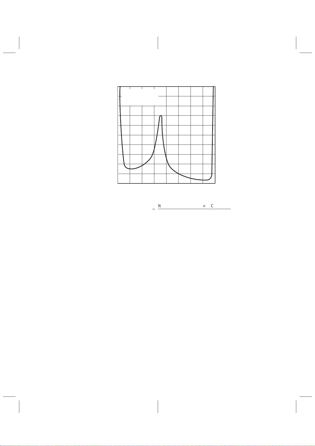
5–7
0.5
0.4
0.2
0.1
0
0.9
0.3
01 2 34 5 6
Time – ms
0.7
0.6
0.8
1
7
8
TA = 25°C
fs = 8 kHz
FCLK = 144 kHz
ADC BAND-PASS GROUP DELAY
fi – Input Frequency – kHz
NOTE A : Absolute Frequency (kHz)
+
Normalized Frequency FCLK (kHz)
144
Figure 5–7

5–8
012345 6
DAC LOW-PASS RESPONSE
78910
–10
–20
–30
–40
–50
–60
0
Attenuation – dB
TA = 25°C
fs = 9.6 kHz
FCLK = 144 kHz
fi – Input Frequency – kHz
NOTE A : Absolute Frequency (kHz)
+
Normalized Frequency FCLK (kHz)
144
Figure 5–8

5–9
0
0 0.5 1 1.5 2 2.5 3
0.2
0.4
0.5
3.5 4
0.3
0.1
–0.1
–0.2
–0.3
–0.4
–0.5
Attenuation – dB
TA = 25°C
fs = 9.6 kHz
FCLK = 144 kHz
fi – Input Frequency – kHz
DAC LOW-PASS RESPONSE
NOTE A : Absolute Frequency (kHz)
+
Normalized Frequency FCLK (kHz)
144
Figure 5–9

5–10
0.5
0.4
0.2
0.1
0
0.9
0.3
0123456
Time – ms
0.7
0.6
0.8
1
78910
TA = 25°C
fs = 9.6 kHz
FCLK = 144 kHz
DAC LOW-PASS GROUP DELAY
fi – Input Frequency – kHz
NOTE A : Absolute Frequency (kHz)
+
Normalized Frequency FCLK (kHz)
144
Figure 5–10

5–11
Normalized Frequency
– 2
– 4
– 6
0 2 4 6 8 10 12
Magnitude – dB
0
2
4
14 16 18 20
TA = 25°C
Input = ± 3-V Sine Wave
DAC (sin x)/x CORRECTION FILTER RESPONSE
NOTE A : Absolute Frequency (kHz)
+
Normalized Frequency FCLK (kHz
)
288
Figure 5–11

5–12
Normalized Frequency
200
100
0
0 2 4 6 8 10 12
Group Delay –
300
400
500
14 16 18 20
sµ
TA = 25°C
Input = ± 3-V Sine Wave
DAC (sin x)/x CORRECTION FILTER RESPONSE
NOTE A : Absolute Frequency (kHz)
+
Normalized Frequency FCLK (kHz)
288
Figure 5–12
5–13
0
– 0.4
–1.2
–1.6
– 2
1.6
– 0.8
0123456
Magnitude – dB
0.8
0.4
1.2
2
78910
(sin x) /x Correction
Error
TA = 25°C
Input = ± 3-V Sine Wave
Normalized Frequency
19.2-kHz (sin x) /x
Distortion
DAC (sin x)/x CORRECTION ERROR
NOTE A : Absolute Frequency (kHz)
+
Normalized Frequency FCLK (kHz)
288
Figure 5–13

5–14

6–1
6 Application Information
TMS320C2x/3x
CLKOUT
DX
DR
FSX
FSR
CLKX
CLKR
TLC320AC01
MCLK
DIN
DOUT
FS
SCLK
5 V
0.1 µF
5 V
5 V
D
GND
A
GND
DAC V
DD
DAC V
MID
DAC GND
ADC V
DD
ADC V
MID
ADC GND
DGTL V
DD
DGTL GND
0.1 µF
0.1 µF
0.1 µF
0.1 µF
14
10
11
12
13
5
6
7
9
24
23
22
20
NOTE A: Terminal numbers shown are for the FN package.
Figure 6–1. Stand-Alone Mode (to DSP Interface)
TMS320C2x/3x
CLKOUT
DX
DR
FSX
FSR
CLKX
CLKR
TLC320AC01
MCLK
DIN
DOUT
FS
SCLK
14
10
11
12
13
NOTE A: Terminal numbers shown are for the FN package.
Figure 6–2. Codec Mode (to DSP Interface)
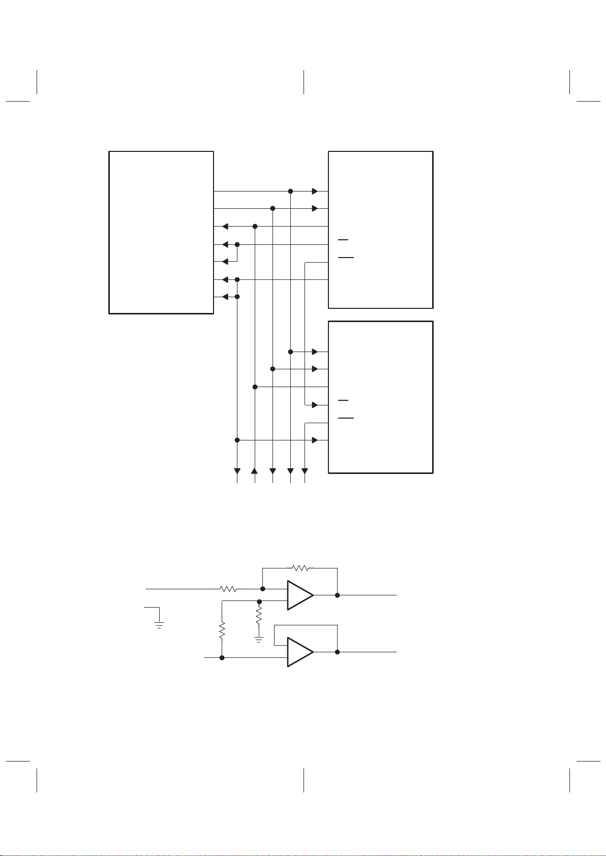
6–2
TMS320C2x/3x
CLKOUT
DX
DR
FSX
FSR
CLKX
CLKR
TLC320AC01
MCLK
DIN
DOUT
FS
SCLK
FSD
TLC320AC01
MCLK
DIN
DOUT
FS
SCLK
FSD
Master Mode
Slave Mode
14
10
11
12
13
14
10
11
12
13
NOTE A: Terminal numbers shown are for the FN package.
Figure 6–3. Master With Slave (to DSP Interface)
+
–
+
–
10 kΩ
10 kΩ
TLE2022
TLE2022
ADC V
MID
IN+
IN–
10 kΩ
10 kΩ
+
V
I
†
–
†
The VI source must be capable of sinking a current equal to [ADC V
MID
+ |VI|(max)]/10 kΩ.
Figure 6–4. Single-Ended Input (Ground Referenced)

6–3
+
–
+
–
10 kΩ
TLE2064
4
IN–
IN+
ADC V
MID
10 kΩ
10 kΩ
10 kΩ
10 kΩ
10 kΩ
+
–
TLE2064
4
TLE2064
4
V
I
†
†
The VI source must be capable of sinking a current equal to [(ADC V
MID
/2) + |VI|(max)]/10 kΩ.
Figure 6–5. Single-Ended to Differential Input (Ground Referenced)
OUT–
OUT+
600-Ω
Load
Figure 6–6. Differential Load
+
–
10 kΩ
TLE2062
OUT–
OUT+
600-Ω
Load
10 kΩ
10 kΩ
10 kΩ
5 V
– 5 V
NOTE A: When a signal changes from a single supply with a nonzero reference system to a
grounded load, the operational amplifier must be powered from plus and minus supplies
or the load must be capacitively coupled.
Figure 6–7. Differential Output Drive (Ground Referenced)

6–4
+
–
TLE2062
OUT+
OUT–
600-Ω
Load
+
–
TLE2062
Figure 6–8. Low-Impedance Output Drive
+
–
100 kΩ
TLE2062
OUT+
DAC V
MID
Load
100 kΩ
100 kΩ
100 kΩ
NOTE A: When a signal changes from a single supply with a nonzero reference system to a
grounded load, the operational amplifier must be powered from plus and minus supplies
or the load must be capacitively coupled.
600-Ω
5 V
– 5 V
Figure 6–9. Single-Ended Output Drive (Ground Referenced)
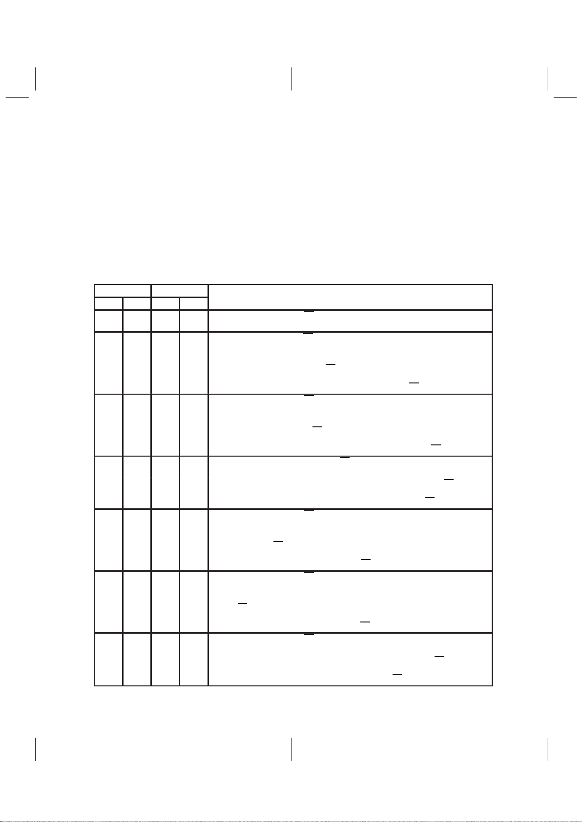
A–1
Appendix A
Primary Control Bits
The function of the primary-word control bits D01 and D00 and the hardware terminals FC0 and FC1 are
shown below. Any combinational state of D01, D00, FC1, and FC0 not shown is ignored.
CONTROL FUNCTION OF CONTROL BITS
BITS TERMINALS
D01 D00 FC1 FC0
0 0 0 0 On the next falling edge of FS, the AIC receives DAC data D15–D02 to DIN and
transmits the ADC data D15–D00 from DOUT.
0 0 0 1
On the next falling edge of FS, the AIC receives DAC data D15–D02 to DIN and
transmits the ADC data D15–D00 from DOUT.
The phase adjustment is determined by the state of FC1 and FC0 such that on the
next rising edge of the next internal FS
, the next ADC/DAC sampling time occurs later
by the number of MCLK periods equal to the value contained in the A′ register. When
the A′ register value is negative, the internal falling edge of FS
occurs earlier.
0 0 1 0
On the next falling edge of FS, the AIC receives DAC data D15 –D02 at DIN and
transmits the ADC data D15–D00 from DOUT.
The phase adjustment is determined by the state of FC1 and FC0 such that on the
rising edge of the next internal FS
, the next ADC/DAC sample time occurs earlier by
the number of MCLK periods determined by the value contained in the A′ register.
When the A′ register value is negative, the internal falling edge of FS
occurs later.
0 0 1 1
On the next falling edge of the primary FS, the AIC receives DAC data D15–D02 at
DIN and transmits the ADC data D15–D00 from DOUT.
When FC0 and FC1 are both taken high, the AIC initiates a secondary FS to receive
a secondary control word at DIN. The secondary frame sync occurs at 1/2 the
sampling time as measured from the falling edge of the primary FS
.
0 1 0 0
On the next falling edge of FS, the AIC receives DAC data D15 –D02 to DIN and
transmits the ADC data D15–D00 from DOUT.
The phase adjustment is determined by the state of D01 and D00 such that on the
next rising edge of FS
, the next ADC/DAC sampling time occurs later by the number
of MCLK periods determined by the value contained in the A′ register. When the A′
register value is negative, the falling edge of FS
occurs earlier.
1 0 0 0
On the next falling edge of FS, the AIC receives DAC data D15 –D02 at DIN and
transmits the ADC data D15–D00 from DOUT.
The phase adjustment is determined by the state of D01 and D00. On the next rising
edge of FS
, the next ADC/DAC sampling time occurs earlier by the number of MCLK
periods determined by the value contained in the A′ register. When the A′ register
value is negative, the internal falling edge of FS
occurs later.
1 1 0 0
On the next falling edge of FS, the AIC receives DAC data D15 –D02 to DIN and
transmits the ADC data D15–D00 from DOUT.
When D00 and D01 are both high, the AIC initiates a secondary FS to receive a
secondary control word at DIN. The secondary frame sync occurs at 1/2 the sampling
time as measured from the falling edge of the primary FS
.

A–2
CONTROL FUNCTION OF CONTROL BITS (Continued)
BITS TERMINALS
D01 D00 FC1 FC0
0 1 1 1
On the next falling edge of FS, the AIC receives DAC data D15–D02 to DIN and
transmits the ADC data D15–D00 from DOUT.
The phase adjustment is determined by the state of D01 and D00 such that on the
next rising edge of FS
, the next ADC/DAC sampling time occurs later by the number
of MCLK periods determined by the value contained in the A′ register. When the A′
register value is negative, FS
occurs earlier.
When FC0 and FC1 are both taken high, the AIC initiates a secondary FS to receive
a secondary control word at DIN. The secondary frame sync occurs at 1/2 the
sampling time as measured from the falling edge of the primary FS
.
1 0 1 1
On the next falling edge of FS, the AIC receives DAC data D15 –D02 at DIN and
transmits the ADC data D15–D00 from DOUT.
The phase adjustment is determined by the state of D01 and D00. On the next rising
edge of FS
, the next ADC/DAC sample time occurs earlier by the number of MCLK
periods determined by the value contained in the A′ register. When the A′ register
value is negative, FS
occurs later.
When FC0 and FC1 are both taken high, the AIC initiates a secondary FS to receive
a secondary control word at DIN. The secondary frame sync occurs at 1/2 the
sampling time as measured from the falling edge of the primary FS
.
1 1 1 1
On the next falling edge of the primary FS, the AIC receives DAC data D15–D02 at
DIN and transmits the ADC data D15–D00 from DOUT.
When FC1 and FC0 are both high or D01 and D00 are both high, the AIC initiates a
secondary FS
to receive a secondary control word at DIN. The secondary FS occurs
at 1/2 the sampling time measured from the falling edge of the primary FS
.
1 1 0 1
On the next falling edge of FS, the AIC receives DAC data D15 –D02 to DIN and
transmits the ADC data D15–D00 from DOUT.
When D00 and D01 are high, the AIC initiates a secondary FS to receive a secondary
control word at DIN. The secondary frame sync occurs at 1/2 the sampling time as
measured from the falling edge of the primary FS
.
The phase adjustment is determined by the state of FC1 and FC0 such that on the
next rising edge of FS
, the next ADC/DAC sampling time occurs later by the number
of MCLK periods determined by the value contained in the A′ register. When the A′
register value is negative, FS
occurs earlier.
1 1 1 0
On the next falling edge of FS, the AIC receives DAC data D15–D02 to DIN and
transmits the ADC data D15–D00 from DOUT.
When D00 and D01 are high, the AIC initiates a secondary FS to receive a secondary
control word at DIN. The secondary frame sync occurs at 1/2 the sampling time as
measured from the falling edge of the primary FS
.
The phase adjustment is determined by the state of FC1 and FC0 such that on the
next rising edge of FS
, the next ADC/DAC sampling time occurs later by the number
of MCLK periods determined by the value contained in the A′ register. When the A′
register value is negative, FS
occurs earlier.
1 1 1 1
On the next falling edge of FS, the AIC receives DAC data D15 –D02 at DIN and
transmits the ADC data D15–D00 from DOUT.
When FC1 and FC0 are both high or D01 and D00 are both high, the AIC initiates a
secondary FS
to receive a secondary control word at DIN. The secondary FS occurs
at 1/2 the sampling time measured from the falling edge of the primary FS
.

B–1
Appendix B
Secondary Communications
The function of the control bits DS15 and DS14 and the hardware terminals FC0 and FC1 are shown below.
Any combinational state of DS15, DS14, FC1, and FC0 not shown is ignored.
CONTROL FUNCTION OF SECONDARY COMMUNICATION
BITS TERMINALS
DS15 DS14 FC1 FC0
0 0 Ignored On the next falling edge of FS, the AIC receives DAC data D15–D02 at DIN and
transmits the ADC data D15–D00 from DOUT.
0 1 Ignored
On the next falling edge of the FS, the AIC receives DAC data D15–D02 at DIN and
transmits the ADC data D15–D00 from DOUT.
The phase adjustment is determined by the state of DS15 and DS14 such that on the
next rising edge of FS
, the next ADC/DAC sampling time occurs later by the number
of MCLK periods determined by the value contained in the A′ register. When the A′
register value is negative, FS
occurs earlier.
1 0 Ignored
On the next falling edge of FS, the AIC receives DAC data D15 –D02 at DIN and
transmits the ADC data D15–D00 from DOUT.
The phase adjustment is determined by the state of D01 and D00. On the next rising
edge of FS
, the next ADC/DAC sampling time occurs earlier by the number of MCLK
periods determined by the value contained in the A′ register. When the A′ register
value is negative, FS
occurs later.
1 1 0 0 On the next falling edge of FS, the AIC receives DAC data D15–D02 at DIN and
transmits the ADC data D15–D00 from DOUT.
1 1 0 1
On the next falling edge of the FS, the AIC receives DAC data D15–D02 at DIN and
transmits the ADC data D15–D00 from DOUT.
The phase adjustment is determined by the state of FC1 and FC0 such that on the
next rising edge of FS
, the next ADC/DAC sampling time occurs later by the number
of MCLK periods determined by the value contained in the A′ register. When the A′
register value is negative, FS
occurs earlier.
1 1 1 0
On the next falling edge of FS, the AIC receives DAC data D15 –D02 at DIN and
transmits the ADC data D15–D00 from DOUT.
The phase adjustment is determined by the state of FC1 and FC0 such that on the
next rising edge of FS
, the next ADC/DAC sampling time occurs earlier by the number
of MCLK periods determined by the value contained in the A′ register. When the A′
register value is negative, FS
occurs later.
1 1 1 1 On the next falling edge of FS, the AIC receives DAC data D15–D02 at DIN and
transmits the ADC data D15–D00 from DOUT.

B–2

C–1
Appendix C
TLC320AC01C/TLC320AC02C Specification Comparisons
T exas Instruments manufactures the TLC320AC01C and the TLC320AC02C specified for the 0°C to 70°C
commercial temperature range and the TLC320AC02I specified for the –40°C to 85°C temperature range.
The TLC320AC02C and TLC320AC02I operate at a relaxed TLC320AC01C specification. The differences
are listed in the following tables.
ADC Channel Signal-to-Distortion Ratio, VDD = 5 V, fs = 8 kHz (Unless
Otherwise Noted) (see Note 1)
AV = 0 dB AV = 6 dB AV = 12 dB
PARAMETER
TEST CONDITIONS
MIN MAX MIN MAX MIN MAX
UNIT
TLC320AC01
68 — —
TLC320AC02
V
I
= –6 dB to –1
dB
64 — —
TLC320AC01
63 68 —
TLC320AC02
V
I
= –
12 dB to –6 dB
59 64 —
TLC320AC01
57 63 68
TLC320AC02
V
I
= –18 dB to –12
dB
56 59 64
TLC320AC01
51 57 63
TLC320AC02
V
I
= –24 dB to –18
dB
50 56 59
TLC320AC01
45 51 57
dB
TLC320AC02
V
I
= –
30 dB to –24 dB
44 50 56
TLC320AC01
39 45 51
TLC320AC02
V
I
= –36 dB to –30
dB
38 44 50
TLC320AC01
33 39 45
TLC320AC02
V
I
= –42 dB to –36
dB
32 38 44
TLC320AC01
27 33 39
TLC320AC02
V
I
= –48 dB to –42
dB
26 32 38
NOTE 1: The analog-input test signal is a 1020-Hz sine wave with 0 dB = 6 V peak to peak as the reference level for
the analog input signal.

C–2
DAC Channel Signal-to-Distortion Ratio, VDD = 5 V, fs = 8 kHz (Unless
Otherwise Noted) (see Note 2)
AV = 0 dB AV = –6 dB AV = –12 dB
PARAMETER
TEST CONDITIONS
MIN MAX MIN MAX MIN MAX
UNIT
TLC320AC01
68 — —
TLC320AC02
V
O
= –
6 dB to 0 dB
64 — —
TLC320AC01
63 68 —
TLC320AC02
V
O
= –12 dB to –6
dB
59 64 —
TLC320AC01
57 63 68
TLC320AC02
V
O
= –18 dB to –12
dB
56 59 64
TLC320AC01
51 57 63
TLC320AC02
V
O
= –
24 dB to –18 dB
50 56 59
TLC320AC01
45 51 57
dB
TLC320AC02
V
O
= –30 dB to –24
dB
44 50 56
TLC320AC01
39 45 51
TLC320AC02
V
O
= –36 dB to –30
dB
38 44 50
TLC320AC01
33 39 45
TLC320AC02
V
O
= –
42 dB to –36 dB
32 38 44
TLC320AC01
27 33 39
TLC320AC02
V
O
= –48 dB to –42
dB
26 32 38
NOTE 2: The input signal, VI, is the digital equivalent of a 1020-Hz sine wave (full-scale analog output at full-scale digital
input = 0 dB). The nominal differential DAC channel output with this input condition is 6 V peak to peak. The
load impedance for the DAC output buffer is 600 Ω from OUT+ to OUT –.

C–3
System Distortion, ADC Channel Attenuation, VDD = 5 V, fs = 8 kHz,
FCLK = 144 kHz (Unless Otherwise Noted)
PARAMETER TEST CONDITIONS MIN MAX UNIT
TLC320AC01
70 dB
TLC320AC02
Second harmonic
Differential input
64 dB
TLC320AC01
(see Note 3)
70 dB
TLC320AC02
Third harmonic and higher harmonics
64 dB
NOTE 3: The input signal is a 1020 Hz-sine wave for the ADC channel. Harmonic distortion is defined for an input level
of –1 dB.
System Distortion, DAC Channel Attenuation, VDD = 5 V, fs = 8 kHz,
FCLK = 144 kHz (Unless Otherwise Noted)
PARAMETER TEST CONDITIONS MIN MAX UNIT
TLC320AC01
70 dB
TLC320AC02
Second harmonic
Differential output
64 dB
TLC320AC01
(see Note 4)
70 dB
TLC320AC02
Third harmonic and higher harmonics
64 dB
NOTE 4: The input signal is the digital equivalent of a 1020-Hz sine wave (digital full scale = 0 dB). The nominal
differential DAC channel output with this input condition is 6 V peak to peak. The load impedance for the DAC
output buffer is 600 Ω from OUT+ to OUT–. Harmonic distortion is specified for a signal input level of 0 dB.

C–4

D–1
Appendix D
Multiple TLC320AC01/02 Analog Interface Circuits on One
TMS320C5X DSP Serial Port
In many applications, digital signal processors (DSP) must obtain information from multiple analog-to-digital
(A/D) channels and transmit digital data to multiple digital-to-analog (D/A) conversion channels. The
problem is how to do it easily and efficiently.
This application report addresses the issue of connecting two channels of an analog interface circuit (AIC)
to one TMS320C5X DSP serial port. In this application report, the AIC is the TLC320AC01.
The TLC320AC01 (and TLC320AC02) analog interface circuit contains both A/D and D/A converters and
using the master/slave mode, it is possible to connect two of them to one TMS320C5X DSP serial port with
no additional logic. The hardware schematic is shown in Figure D–1.

D–2
TMS320C5x
CLKOUT
DX
DR
FSX
FSR
CLKX
CLKR
TLC320AC01
MCLK
DIN
DOUT
FS
SCLK
FSD
TLC320AC01
MCLK
DIN
DOUT
FS
SCLK
FSD
Master Mode
Slave Mode
14
10
11
12
13
14
10
11
12
13
NOTE A: Terminal numbers shown are for the FN package.
Figure D–1. Master With Slave (to DSP Interface)
HARDWARE AND SOFTWARE SOLUTION
Once the hardware connections are completed, the issue becomes distinguishing one channel from
another. Fortunately, this is very easy to do in software and adds very little overhead. The mode that the
AC01s run in is called master/slave mode. One AC01 is the master and all of the rest of the AC01s are
slaves. The master can be distinguished from all of the slaves by examining the least significant bit (LSB)
in the receive word coming from the AC01. The master has a 0 in the LSB and all of the slaves have a 1
in the LSB.
The AC01s in master/slave mode take turns communicating with the DSP serial port. They do this is a round
robin or circular fashion. Synchronizing the system involves looking for the master AC01 and then starting
the software associated with the first AC01. All other AC01s follow in order. It is possible to have different
software for each AC01.
A reference design was constructed using a TMS320C5X DSP starter kit (DSK). The AC01s were
connected to the TDM serial port which is available at the headers on the edge of the DSK.
A listing of the DSK assembly code for a simple stereo input/output program is included in the following
section.

D–3
SOFTWARE MODULE
MODULE NAME: INOUTB.ASM
In-out routine for C5X DSK with two TLC320AC01s on the
TDM serial port of the C5X in master/slave mode.
This version performs the in/out task for both the master
and slave TLC320AC01 in the receive interrupt service
routine.
*****************************************************************************
*******************
*****************************************************************************
*******************
* .mmregs
.ds 01000h
PR1 .word 0104h ;A register
PR2 .word 0219h ;B register
PR3 .word 0300h ;A prime register
PR4 .word 0405h ;amplifier gain register
PR5 .word 0501h ;analog configuration register
PR6 .word 0600h ;digital configuration register
PR7 .word 0730h ;frame synch delay register
PR8 .word 0802h ;frame synch number register
value .word 0800h
value2 .word 0800h
val_add .word 0200h
val_add2 .word 0400h
****************************************************************************
******
****************************************************************************
Set up the ISR vector
.ps 080ah
rint: B RECEIVE ; 0A; Serial port receive interrupt RINT.
xint: B TRANSMIT ; 0C; Serial port transmit interrupt XINT.
trint: B TDMREC
txint: B TDMTX
;
*
*****************************************************************************
******
*****************************************************************************
TMS320C5X INITIALIZATION
.ps 0a00h
.entry
START: SETC INTM ; Disable interrupts
LDP #0 ; Set data page pointer
OPL #0834h,PMST
LACC #0
SAMM CWSR
SAMM PDWSR

D–4
splk #00c8h
SPLK 082h,IMR
call AC01INIT
CLRC OVM ; OVM = 0
SPM 0 ; PM = 0
SPLK #042h,IMR ; TDMA ser port rec interrupt
SPLK #0C8h,TSPC ;
CLRC INTM ; enable interrupts
loop ; main program here does nothing.
nop ; a user program can be inserted.
b loop ;
;
end of main program ;
;
; TDM serial port receiver interrupt service routine
;
TDMREC:
; This loop insures that the master AC01
ldp #trcv ; is the first one that is written to in the
bit trcv,15 ; loop. the slave AC01(s) will follow in
bcnd xxx,tc ; sequential order. The master AC01 has a
; 0 in the 1sb. the slave AC01(s) have a 1
; in the 1sb of the receive word.
ldp #trcv
lacc trcv
and #0fffch
;
; user code would go here for master AC01
;
sacl tdxr
b yyy
xxx
ldp #trcv
lacc trcv
and #0fffch
;
; user code would go here for slave AC01
;
sacl tdxr
yyy
rete

D–5
;
; TDM serial port transmit interrupt service routine
;
TDMTX:
rete
;
; RECEIVER INTERRUPT SERVICE ROUTINE
;
RECEIVE:
rete
TRANSMIT:
RETE

D–6
AC01INIT
SPLK #020h,TCR
SPLK #01h,PRD
MAR *,AR0
LACC #0008h
SACL TSPC
LACC #00c8h
SACL TSPC
SETC SXM
;
LDP #PR1
LACC PR1
CALL AC01_2ND
;
LDP #PR2
LACC PR2
CALL AC01_2ND
;
LDP #PR8
LACC PR8
CALL AC01_2ND
;
LDP #PR7
LACC PR7
CALL AC01_2ND
ret
AC01_2ND:
LDP #0
SACH TDXR ;
CLRC INTM
IDLE
ADD #6h, 15 ; 0000 0000 0000 0011 XXXX XXXX XXXX XXXX b
SACH TDXR ;
IDLE
SACL TDXR ;
IDLE
LACL #0 ;
SACL TDXR ; make sure the word got sent
IDLE
SETC INTM ;
RET

D–7

E–1
Appendix E
Mechanical Data
PLASTIC J-LEADED CHIP CARRIER
FN/S-PQCC-J**
4040005/A–07/93
20-PIN SHOWN
0.048 (1,22)
0.042 (1,07)
× 45°
1319
4
8
913
14
18
D3/E
3
D2/E
2
0.020 (0,51) MIN
0.120 (3,05) MAX
0.180 (4,57) MAX
0.050 (1,27) TYP
D
D
1
E
1
E
JEDEC
OUTLINE PINS**
NO. OF
D/E
MIN MAX
MO-047AA
20
0.385
(9,78)
0.395
(10,03)
0.350
(8,89)
0.356
(9,04)
0.456
(11,58)
0.450
(11,43)
0.495
(12,57)
0.485
(12,32)
28
MO-047AB
44
MO-047AC
52
MO-047AD
0.390
(9,91)
0.430
(10,92)
0.300
(7,62)
0.200
(5,08)
0.330
(8,38)
0.290
(7,34)
0.890
(22,61)
0.930
(23,62)
0.800
(20,32)
1.000
(25,40)
1.130
(28,70)
1.090
(27,69)
MO-047AF 84
1.185
(30,10)
1.195
(30,35)
1.150
(29,21)
1.158
(29,41)
0.956
(24,28)
0.950
(24,13)
0.995
(25,27)
0.985
(25,02)
68MO-047AE
0.500
(12,70)
0.630
(16,00)
0.590
(14,99)
0.685
(17,40)
0.695
(17,65)
0.650
(16,51)
0.656
(16,66)
0.600
(15,24)
0.730
(18,54)
0.690
(17,53)
0.785
(19,94)
0.795
(20,19)
0.750
(19,05)
0.756
(19,20)
D2/E
2
D3/E
3
D1/E
1
MIN MAX MIN MAX TYP
NOTES: A. All linear dimensions are in inches (millimeters).
B. This drawing is subject to change without notice.
C. Dimensions D1 and E1 do not include mold flash or protrusion. Protrusion shall not exceed 0.010 (0,25)
on any side.
D. All dimensions conform to JEDEC Specification MO-047.
E. Maximum deviation from coplanarity is 0.004 (0,10).
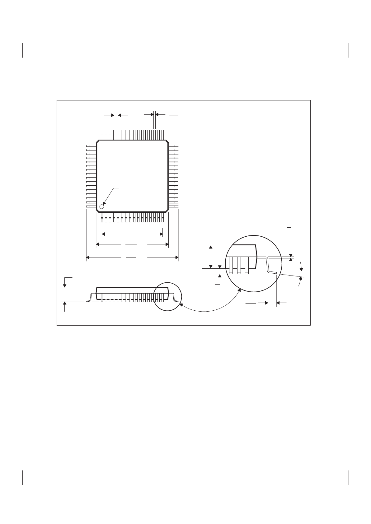
E–2
4040152/A–07/93
0,70
0,30
11,80
12,20
48 33
49
64
116
32
17
Pin # 1
Indicator
10,10
9,90
0,50 TYP
0,00 MIN
PLASTIC QUAD FLAT PACKAGEPM/S-PQFP-G64
SQ
SQ
7,50 SQ TYP
0,147
0,177
0,14
0,26
1,70 MAX
0°–10°
Seating Plane
1,30
1,50
NOTES: A. All linear dimensions are in millimeters.
B. This drawing is subject to change without notice.
C. Maximum deviation from coplanarity is 0,08 mm.
D. Body dimensions do not include mold flash or protrusion.

IMPORTANT NOTICE
T exas Instruments and its subsidiaries (TI) reserve the right to make changes to their products or to discontinue
any product or service without notice, and advise customers to obtain the latest version of relevant information
to verify, before placing orders, that information being relied on is current and complete. All products are sold
subject to the terms and conditions of sale supplied at the time of order acknowledgement, including those
pertaining to warranty, patent infringement, and limitation of liability.
TI warrants performance of its semiconductor products to the specifications applicable at the time of sale in
accordance with TI’s standard warranty. T esting and other quality control techniques are utilized to the extent
TI deems necessary to support this warranty. Specific testing of all parameters of each device is not necessarily
performed, except those mandated by government requirements.
CERT AIN APPLICATIONS USING SEMICONDUCTOR PRODUCTS MAY INVOLVE POTENTIAL RISKS OF
DEATH, PERSONAL INJURY, OR SEVERE PROPERTY OR ENVIRONMENTAL DAMAGE (“CRITICAL
APPLICATIONS”). TI SEMICONDUCTOR PRODUCTS ARE NOT DESIGNED, AUTHORIZED, OR
WARRANTED TO BE SUITABLE FOR USE IN LIFE-SUPPORT DEVICES OR SYSTEMS OR OTHER
CRITICAL APPLICATIONS. INCLUSION OF TI PRODUCTS IN SUCH APPLICA TIONS IS UNDERST OOD TO
BE FULLY AT THE CUSTOMER’S RISK.
In order to minimize risks associated with the customer’s applications, adequate design and operating
safeguards must be provided by the customer to minimize inherent or procedural hazards.
TI assumes no liability for applications assistance or customer product design. TI does not warrant or represent
that any license, either express or implied, is granted under any patent right, copyright, mask work right, or other
intellectual property right of TI covering or relating to any combination, machine, or process in which such
semiconductor products or services might be or are used. TI’s publication of information regarding any third
party’s products or services does not constitute TI’s approval, warranty or endorsement thereof.
Copyright 1998, Texas Instruments Incorporated
 Loading...