

查询TLC2652供应商
TLC2652, TLC2652A, TLC2652Y
Advanced LinCMOS PRECISION CHOPPER-STABILIZED
OPERATIONAL AMPLIFIERS
SLOS019C – SEPTEMBER 1988 – REVISED FEBRUARY 1999
D
Extremely Low Offset Voltage ...1 µV Max
D
Extremely Low Change on Offset Voltage
With Temperature . . . 0.003 µV/°C Typ
D
Low Input Offset Current
500 pA Max at T
D
AVD. . . 135 dB Min
D
CMRR and k
D
Single-Supply Operation
D
Common-Mode Input Voltage Range
SVR
= – 55°C to 125°C
A
. . . 120 dB Min
Includes the Negative Rail
D
No Noise Degradation With External
Capacitors Connected to V
DD–
description
The TLC2652 and TLC2652A are high-precision
chopper-stabilized operational amplifiers using
Texas Instruments Advanced LinCMOS
process. This process in conjunction with unique
chopper-stabilization circuitry produces opera
tional amplifiers whose performance matches or
exceeds that of similar devices available today.
Chopper-stabilization techniques make possible
extremely high dc precision by continuously
nulling input offset voltage even during variation in
temperature, time, common-mode voltage, and
power supply voltage. In addition, low-frequency
noise voltage is significantly reduced. This high
precision, coupled with the extremely high input
impedance of the CMOS input stage, makes the
TLC2652 and TLC2652A an ideal choice for
low-level signal processing applications such as
strain gauges, thermocouples, and other
transducer amplifiers. For applications that
require extremely low noise and higher usable
bandwidth, use the TLC2654 or TLC2654A
device, which has a chopping frequency of
10 kHz.
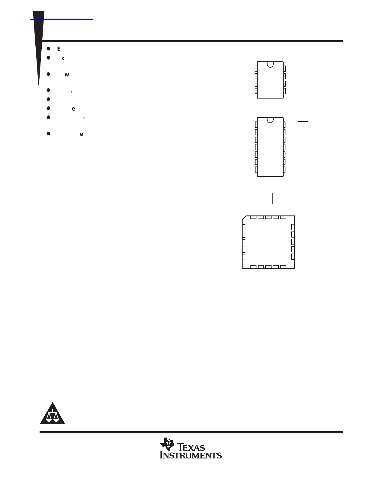
D008, JG, OR P PACKAGE
(TOP VIEW)
C
V
DD–
D014, J, OR N PACKAGE
V
NC
NC
IN–
NC
IN+
NC – No internal connection
1
XA
IN–
2
IN+
3
4
(TOP VIEW)
C
1
XB
C
2
XA
NC
3
IN–
4
IN+
5
NC
6
7
DD–
FK PACKAGE
(TOP VIEW)
XA
XB
V
V
3212019
4
5
6
7
8
910111213
NC
DD–
V
8
7
6
5
14
13
12
11
10
9
8
INT/EXT
NC
NC
C RETURN
C
XB
V
DD+
OUT
CLAMP
INT/EXT
CLK IN
CLK OUT
V
DD+
OUT
CLAMP
C RETURN
CLK IN
CLK OUT
18
NC
17
V
16
DD+
NC
15
OUT
14
CLAMP
The TLC2652 and TLC2652A input common-mode range includes the negative rail, thereby providing superior
performance in either single-supply or split-supply applications, even at power supply voltage levels as low as
±1.9 V.
Two external capacitors are required for operation of the device; however , the on-chip chopper-control circuitry
is transparent to the user. On devices in the 14-pin and 20-pin packages, the control circuitry is made accessible
to allow the user the option of controlling the clock frequency with an external frequency source. In addition, the
clock threshold level of the TLC2652 and TLC2652A requires no level shifting when used in the single-supply
configuration with a normal CMOS or TTL clock input.
Please be aware that an important notice concerning availability, standard warranty, and use in critical applications of
Texas Instruments semiconductor products and disclaimers thereto appears at the end of this data sheet.
Advanced LinCMOS is a trademark of Texas Instruments Incorporated.
PRODUCTION DATA information is current as of publication date.
Products conform to specifications per the terms of Texas Instruments
standard warranty. Production processing does not necessarily include
testing of all parameters.
POST OFFICE BOX 655303 • DALLAS, TEXAS 75265
Copyright 1999, Texas Instruments Incorporated
On products compliant to MIL-PRF-38535, all parameters are tested
unless otherwise noted. On all other products, production
processing does not necessarily include testing of all parameters.
1
TLC2652, TLC2652A, TLC2652Y
VIOmax
1 µV
TLC2652AC-8D
TLC2652ACP
TLC2652AC-14D
TLC2652ACN
3 µV
TLC2652C-8D
TLC2652CP
TLC2652C-14D
TLC2652CN
1 µV
TLC2652AI-8D
TLC2652AIP
TLC2652AI-14D
TLC2652AIN
3 µV
TLC2652A-8D
TLC2652IP
TLC2652I-14D
TLC2652IN
µ
to
µ
Advanced LinCMOS PRECISION CHOPPER-STABILIZED
OPERATIONAL AMPLIFIERS
SLOS019C – SEPTEMBER 1988 – REVISED FEBRUARY 1999
description (continued)
Innovative circuit techniques are used on the TLC2652 and TLC2652A to allow exceptionally fast overload
recovery time. If desired, an output clamp pin is available to reduce the recovery time even further.
The device inputs and output are designed to withstand –100-mA surge currents without sustaining latch-up.
Additionally the TLC2652 and TLC2652A incorporate internal ESD-protection circuits that prevent functional
failures at voltages up to 2000 V as tested under MIL-STD-883C, Method 3015.2; however, care should be
exercised in handling these devices as exposure to ESD may result in degradation of the device parametric
performance.
The C-suffix devices are characterized for operation from 0°C to 70°C. The I-suffix devices are characterized
for operation from –40°C to 85°C. The Q-suffix devices are characterized for operation from –40°C to125°C.
The M-suffix devices are characterized for operation over the full military temperature range of –55°C to125°C.
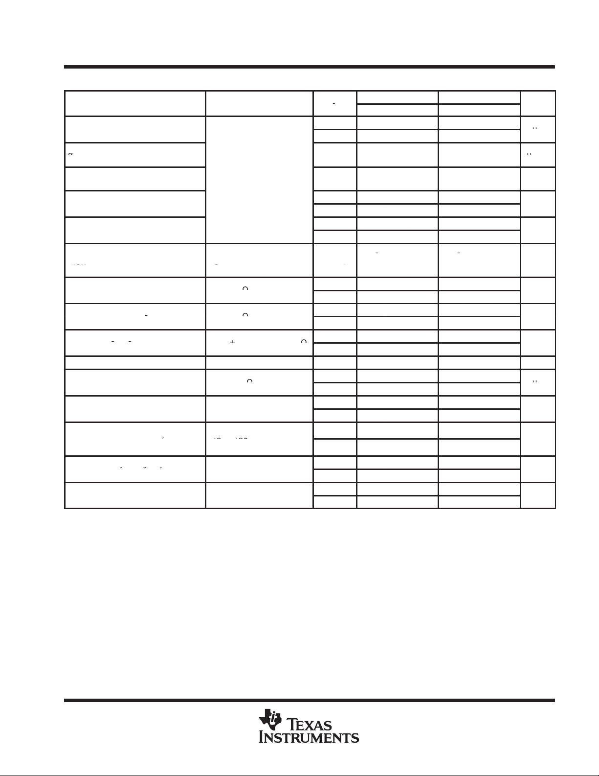
AVAILABLE OPTIONS
PACKAGED DEVICES
T
A
0°C
to
70°C
–40°C
to
85°C
–40°C
to
125°C
–55°C
125°C
AT 25°C
3.5 µV TLC2652Q-8D — — — — — — —
3 µV TLC2652AM-8D TLC2652AMJG TLC2652AMP TLC2652AM-14D TLC2652AMJ TLC2652AMN TLC2652AMFK
3.5 µV TLC2652M-8D TLC2652MJG TLC2652MP TLC2652M-14D TLC2652MJ TLC2652MN TLC2652MFK
SMALL
OUTLINE
(D008)
8 PIN 14 PIN 20 PIN
CERAMIC
DIP
(JG)
—
—
—
—
—
—
PLASTIC
DIP
(P)
SMALL
OUTLINE
(D014)
CERAMIC
DIP
(J)
—
—
—
—
—
—
PLASTIC
DIP
(N)
CHIP
CARRIER
(FK)
—
—
—
—
—
—
The D008 and D014 packages are available taped and reeled. Add R suffix to the device type (e.g., TLC2652AC-8DR). Chips are tested at 25°C.
CHIP
FORM
(Y)
TLC2652Y
—
—
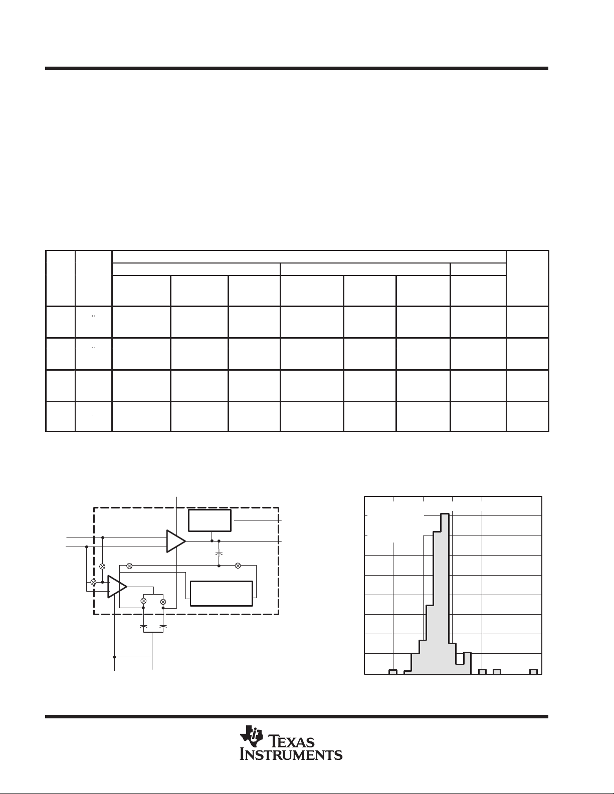
functional block diagram
V
DD+
7
Clamp
3
IN+
IN–
2
B
Main
B
A
+
–
Null
AB
C
XA
4
V
DD–
8
C RETURN
Pin numbers shown are for the D (14 pin), JG, and N packages.
+
–
C
XB
Circuit
C
IC
A
Compensation-
Biasing
Circuit
External Components
5
6
CLAMP
OUT
DISTRIBUTION OF TLC2652
INPUT OFFSET VOLTAGE
36
150 Units Tested From 1 Wafer Lot
32
V
= ±5 V
DD±
TA = 25°C
28
N Package
24
20
16
12
8
Percentage of Units – %
4
0
–3 –2 –1 0 1 2 3
VIO – Input Offset Voltage – µV
2
POST OFFICE BOX 655303 • DALLAS, TEXAS 75265
TLC2652, TLC2652A, TLC2652Y
Advanced LinCMOS PRECISION CHOPPER-STABILIZED
OPERATIONAL AMPLIFIERS
SLOS019C – SEPTEMBER 1988 – REVISED FEBRUARY 1999
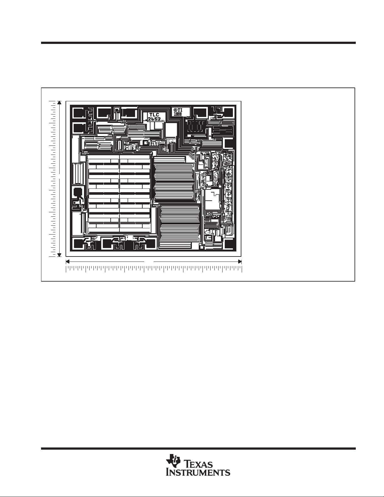
TLC2652Y chip information
This chip, when properly assembled, displays characteristics similar to the TLC2652C. Thermal compression
or ultrasonic bonding may be used on the doped-aluminum bonding pads. Chips may be mounted with
conductive epoxy or a gold-silicon preform.
BONDING PAD ASSIGNMENTS
80
(13)
(14)
(1)
(2)
(12) (11) (10) (9)
90
(8)
(7)(5)(4)
CHIP THICKNESS: 15 TYPICAL
BONDING PADS: 4 × 4 MINIMUM
TJmax = 150°C
TOLERANCES ARE ±10%.
ALL DIMENSIONS ARE IN MILS.
PIN (7) IS INTERNALLY CONNECTED
TO BACKSIDE OF CHIP.
FOR THE PINOUT, SEE THE FUNCTIONAL
BLOCK DIAGRAM.
POST OFFICE BOX 655303 • DALLAS, TEXAS 75265
3
TLC2652, TLC2652A, TLC2652Y
PACKAGE
A
UNIT
Advanced LinCMOS PRECISION CHOPPER-STABILIZED
OPERATIONAL AMPLIFIERS
SLOS019C – SEPTEMBER 1988 – REVISED FEBRUARY 1999
absolute maximum ratings over operating free-air temperature range (unless otherwise noted)
Supply voltage V
Supply voltage V
Differential input voltage, V
Input voltage, V
Voltage range on CLK IN and INT/EXT
Input current, I
Output current, I
Duration of short-circuit current at (or below) 25°C (see Note 3) unlimited. . . . . . . . . . . . . . . . . . . . . . . . . . . . .
Current into CLK IN and INT/EXT
Continuous total dissipation See Dissipation Rating Table. . . . . . . . . . . . . . . . . . . . . . . . . . . . . . . . . . . . . . . . . . .
Operating free-air temperature range, T
Storage temperature range –65°C to 150°C. . . . . . . . . . . . . . . . . . . . . . . . . . . . . . . . . . . . . . . . . . . . . . . . . . . . . . .
Case temperature for 60 seconds: FK package 260°C. . . . . . . . . . . . . . . . . . . . . . . . . . . . . . . . . . . . . . . . . . . . . .
Lead temperature 1,6 mm (1/16 inch) from case for 10 seconds: D, N, or P package 260°C. . . . . . . . . . . . .
Lead temperature 1,6 mm (1/16 inch) from case for 60 seconds: J or JG package 300°C. . . . . . . . . . . . . . . .
†
Stresses beyond those listed under “absolute maximum ratings” may cause permanent damage to the device. These are stress ratings only, and
functional operation of the device at these or any other conditions beyond those indicated under “recommended operating conditions” is not
implied. Exposure to absolute-maximum-rated conditions for extended periods may affect device reliability.
NOTES: 1. All voltage values, except differential voltages, are with respect to the midpoint between V
2. Differential voltages are at IN+ with respect to IN–.
3. The output may be shorted to either supply. Temperature and/or supply voltages must be limited to ensure that the maximum
dissipation rating is not exceeded.
(see Note 1) 8 V. . . . . . . . . . . . . . . . . . . . . . . . . . . . . . . . . . . . . . . . . . . . . . . . . . . . . . . . . . . .
DD+
(see Note 1) –8 V. . . . . . . . . . . . . . . . . . . . . . . . . . . . . . . . . . . . . . . . . . . . . . . . . . . . . . . . . . .
DD–
(any input, see Note 1) ±8 V. . . . . . . . . . . . . . . . . . . . . . . . . . . . . . . . . . . . . . . . . . . . . . . . . . . . . .
I
(each input) ±5 mA. . . . . . . . . . . . . . . . . . . . . . . . . . . . . . . . . . . . . . . . . . . . . . . . . . . . . . . . . . . . . .
I
±50 mA. . . . . . . . . . . . . . . . . . . . . . . . . . . . . . . . . . . . . . . . . . . . . . . . . . . . . . . . . . . . . . . . . . . . . . .
O
(see Note 2) ±16 V. . . . . . . . . . . . . . . . . . . . . . . . . . . . . . . . . . . . . . . . . . . . . . . . . . .
ID
V
DD
– to V
DD–
±5 mA. . . . . . . . . . . . . . . . . . . . . . . . . . . . . . . . . . . . . . . . . . . . . . . . . . . . . . . . . .
: C suffix 0°C to 70°C. . . . . . . . . . . . . . . . . . . . . . . . . . . . . . . . . . . . . . .
A
I suffix –40°C to 85°C. . . . . . . . . . . . . . . . . . . . . . . . . . . . . . . . . . . . . .
Q suffix –40°C to 125°C. . . . . . . . . . . . . . . . . . . . . . . . . . . . . . . . . . . .
M suffix –55°C to 125°C. . . . . . . . . . . . . . . . . . . . . . . . . . . . . . . . . . . .
DD+
and V
DD–
.
+ 5.2 V. . . . . . . . . . . . . . . . . . . . . . . . . . . . . . . . . . . . . .
‡
T
≤ 25°C DERATING FACTOR T
POWER RATING ABOVE TA = 25°CAPOWER RATINGAPOWER RATINGAPOWER RATING
D008 725 mV 5.8 mW/°C 464 mW 377 mW 145 mW
D014 950 mV 7.6 mW/°C 608 mW 494 mW 190 mW
FK 1375 mV 1 1.0 mW/°C 880 mW 715 mW 275 mW
J 1375 mV 11.0 mW/°C 880 mW 715 mW 275 mW
JG 1050 mV 8.4 mW/°C 672 mW 546 mW 210 mW
N 1575 mV 12.6 mW/°C 1008 mW 819 mW 315 mW
P 1000 mV 8.0 mW/°C 640 mW 520 mW 200 mW
recommended operating conditions
C SUFFIX I SUFFIX Q SUFFIX M SUFFIX
MIN MAX MIN MAX MIN MAX MIN MAX
Supply voltage, V
Common-mode input voltage, V
Clock input voltage V
Operating free-air temperature, T
DD±
IC
A
±1.9 ±8 ±1.9 ±8 ±1.9 ±8 ±1.9 ±8 V
V
DD–VDD+
DD–VDD–
0 70 –40 85 –40 125 –55 125 °C
DISSIPATION RATING TABLE
= 70°C T
–1.9 V
+5 V
DD–VDD+
DD–
V
DD–
–1.9 V
+5 V
= 85°C T
DD–VDD+
DD–VDD–
–1.9 V
+5 V
= 125°C
DD–VDD+
DD–VDD–
–1.9 V
+5 V
4
POST OFFICE BOX 655303 • DALLAS, TEXAS 75265
PARAMETER
TEST CONDITIONS
T
†
UNIT
VIOInput offset voltage
V
Full range
0.003
0.03
0.003
0.03µV/°C
IIOInput offset current
pA
IIBInput bias current
pA
C
5to5
ICR
range
S
g
V
R
10 kΩ
See Note 5
V
V
g
R
See Note 5
V
A
gg
V
R
kΩ
dB
Clamp on-state current
R
100 kΩ
A
Clamp off-state current
V
V
pA
CMRR
j
V
V
dB
k
ygj
dB
IDDSupply current
mA
TLC2652, TLC2652A, TLC2652Y
Advanced LinCMOS PRECISION CHOPPER-STABILIZED
OPERATIONAL AMPLIFIERS
SLOS019C – SEPTEMBER 1988 – REVISED FEBRUARY 1999
electrical characteristics at specified free-air temperature, VDD± = ±5 V (unless otherwise noted)
A
p
α
V
f
ch
†
Full range is 0° to 70°C.
NOTES: 4. Typical values are based on the input offset voltage shift observed through 168 hours of operating life test at TA = 150°C extrapolated
Temperature coefficient of
VIO
input offset voltage
Input offset voltage long-term
drift (see Note 4)
p
p
ICR
OM+
OM–
VD
SVR
ommon-mode input voltage
Maximum positive peak
output voltage swing
Maximum negative peak
output voltage swing
Large-signal differential
voltage amplification
Internal chopping frequency 25°C 450 450 Hz
p
p
Common-mode rejection
ratio
Supply-voltage rejection ratio
(∆V
/∆VIO)
DD±
pp
at TA = 25° using the Arrhenius equation and assuming an activation energy of 0.96 eV.
5. Output clamp is not connected.
VIC = 0, RS = 50 Ω
RS = 50 Ω Full range
=
L
= 10 kΩ,
L
O
=
L
O
VO = 0,
IC
RS = 50 Ω
V
DD±
VO = 0,
,
= ±4 V,
= –4 V to 4
=
ICR
= ±1.9 V to ±8 V, 25°C 120 135 120 135
min,
= 10
L
RS = 50 Ω
25°C 0.6 3 0.5 1
Full range 4.35 2.35
25°C
25°C 2 2
Full range 100 100
25°C 4 4
Full range 100 100
25°C 4.7 4.8 4.7 4.8
Full range 4.7 4.7
25°C –4.7 –4.9 –4.7 –4.9
Full range –4.7 –4.7
25°C 120 150 135 150
Full range 120 130
25°C 25 25
Full range 25 25
25°C 100 100
Full range 100 100
25°C 120 140 120 140
Full range 120 120
Full range 120 120
25°C 1.5 2.4 1.5 2.4
Full range 2.5 2.5
TLC2652C TLC2652AC
MIN TYP MAX MIN TYP MAX
0.003 0.06 0.003 0.02 µV/mo
–5 –5
to
3.1 3.1
µ
°
p
p
V
µ
p
POST OFFICE BOX 655303 • DALLAS, TEXAS 75265
5
TLC2652, TLC2652A, TLC2652Y
PARAMETER
T
†
UNIT
SR+Positive slew rate at unity gain
V/µs
R
10 kΩ
C
SR–Negative slew rate at unity gain
C
L
100 F
V/µs
V
qg
V/√H
V
q
V
,
f 10 kHz,
L
Advanced LinCMOS PRECISION CHOPPER-STABILIZED
OPERATIONAL AMPLIFIERS
SLOS019C – SEPTEMBER 1988 – REVISED FEBRUARY 1999
operating characteristics specified free-air temperature, V
TEST
CONDITIONS
VO = ±2.3 V ,
L
n
N(PP)
I
n
φm
†
Full range is 0° to 70°C.
NOTE 6: This parameter is tested on a sample basis for the TLC2652A. For other test requirements, please contact the factory . This statement
Equivalent input noise voltage
(see Note 6)
Peak-to-peak equivalent input
noise voltage
Equivalent input noise current f = 10 kHz 25°C 0.004 0.004 fA/√Hz
Gain-bandwidth product
Phase margin at unity gain
has no bearing on testing or nontesting of other parameters.
f = 10 Hz 25°C 94 94 140
f = 1 kHz
f = 0 to 1 Hz 25°C 0.8 0.8
f = 0 to 10 Hz
f = 10 kHz
RL = 10 kΩ,
CL = 100 pF
RL = 10 kΩ,
CL = 100 pF
=
= 100 pF
=
,
A
25°C 2 2.8 2 2.8
Full range 1.5 1.5
25°C 2.3 3.1 2.3 3.1
Full range 1.8 1.8
25°C 23 23 35
25°C 2.8 2.8
25°C 1.9 1.9 MHz
25°C 48° 48 °
= ±5 V
DD±
TLC2652C TLC2652AC
MIN TYP MAX MIN TYP MAX
n
z
µ
6
POST OFFICE BOX 655303 • DALLAS, TEXAS 75265
PARAMETER
TEST CONDITIONS
T
†
UNIT
VIOInput offset voltage
V
Full range
0.003
0.03
0.003
0.03µV/°C
IIOInput offset current
pA
IIBInput bias current
pA
C
t
5to5
ICR
voltage range
S
g
V
R
10 kΩ
See Note 5
V
V
g
R
See Note 5
V
A
gg
V
R
kΩ
dB
Clamp on-state current
R
100 kΩ
A
Clamp off-state current
V
V
pA
CMRR
j
V
V
dB
k
ygj
dB
IDDSupply current
V
0
No load
mA
TLC2652, TLC2652A, TLC2652Y
Advanced LinCMOS PRECISION CHOPPER-STABILIZED
OPERATIONAL AMPLIFIERS
SLOS019C – SEPTEMBER 1988 – REVISED FEBRUARY 1999
electrical characteristics at specified free-air temperature, VDD± = ±5 V (unless otherwise noted)
A
p
α
V
†
Full range is –40° to 85°C.
NOTES: 4. Typical values are based on the input offset voltage shift observed through 168 hours of operating life test at TA = 150°C extrapolated
Temperature coefficient of
VIO
input offset voltage
Input offset voltage
long-term drift (see Note 4)
p
p
ICR
OM+
OM–
VD
SVR
ommon-mode inpu
Maximum positive peak
output voltage swing
Maximum negative peak
output voltage swing
Large-signal differential
voltage amplification
Internal chopping frequency 25°C 450 450 Hz
p
p
Common-mode rejection
ratio
Supply-voltage rejection
ratio (∆V
pp
at TA = 25° using the Arrhenius equation and assuming an activation energy of 0.96 eV.
5. Output clamp is not connected.
DD±
/∆VIO)
VIC = 0, RS = 50 Ω
RS = 50 Ω Full range
=
L
= 10 kΩ,
L
O
=
L
O
VO = 0,
IC
RS = 50 Ω
V
DD±
VO = 0,
O
,
= ±4 V,
= –4 V to 4
=
ICR
= ±1.9 V to ±8 V, 25°C 120 135 120 135
,
=
= 10
L
min,
RS = 50 Ω Full range 120 120
25°C 0.6 3 0.5 1
Full range 4.95 2.95
25°C
25°C 2 2
Full range 150 150
25°C 4 4
Full range 150 150
25°C 4.7 4.8 4.7 4.8
Full range 4.7 4.7
25°C –4.7 –4.9 –4.7 –4.9
Full range –4.7 –4.7
25°C 120 150 135 150
Full range 120 125
25°C 25 25
Full range 25 25
25°C 100 100
Full range 100 100
25°C 120 140 120 140
Full range 120 120
25°C 1.5 2.4 1.5 2.4
Full range 2.5 2.5
TLC2652I TLC2652AI
MIN TYP MAX MIN TYP MAX
0.003 0.06 0.003 0.02 µV/mo
–5 –5
to
3.1 3.1
µ
°
p
p
V
µ
p
POST OFFICE BOX 655303 • DALLAS, TEXAS 75265
7

TLC2652, TLC2652A, TLC2652Y
PARAMETER
T
†
UNIT
SR+Positive slew rate at unity gain
V/µs
R
10 kΩ
C
SR–Negative slew rate at unity gain
C
L
100 F
V/µs
V
qg
V/√H
V
q
V
,
f 10 kHz,
L
Advanced LinCMOS PRECISION CHOPPER-STABILIZED
OPERATIONAL AMPLIFIERS
SLOS019C – SEPTEMBER 1988 – REVISED FEBRUARY 1999
operating characteristics at specified free-air temperature, V
TEST
CONDITIONS
VO = ±2.3 V ,
L
n
N(PP)
I
n
φm
†
Full range is –40° to 85°C.
NOTE 6: This parameter is tested on a sample basis for the TLC2652A. For other test requirements, please contact the factory . This statement
Equivalent input noise voltage
(see Note 6)
Peak-to-peak equivalent input
noise voltage
Equivalent input noise current f = 1 kHz 25°C 0.004 0.004 pA/√Hz
Gain-bandwidth product
Phase margin at unity gain
has no bearing on testing or nontesting of other parameters.
f = 10 Hz 25°C 94 94 140
f = 1 kHz
f = 0 to 1 Hz 25°C 0.8 0.8
f = 0 to 10 Hz
f = 10 kHz
RL = 10 kΩ,
CL = 100 pF
RL = 10 kΩ,
CL = 100 pF
=
= 100 pF
=
,
A
25°C 2 2.8 2 2.8
Full range 1.4 1.4
25°C 2.3 3.1 2.3 3.1
Full range 1.7 1.7
25°C 23 23 35
25°C 2.8 2.8
25°C 1.9 1.9 MHz
25°C 48° 48 °
MIN TYP MAX MIN TYP MAX
= ±5 V
DD±
TLC2652I TLC2652AI
n
z
µ
8
POST OFFICE BOX 655303 • DALLAS, TEXAS 75265
A
V
g
V
Full range
0.003
0.03∗0.003
0.03
∗
V/°C
IIOInput offset current
pA
IIBInput bias current
pA
C
t
5to5
ICR
voltage range
S
g
V
R
See Note 5
V
V
g
R
10 kΩ
See Note 5
V
A
gg
V
R
kΩ
dB
Clamp on-state current
V
V
A
Clamp off-state current
R
100 kΩ
pA
CMRR
j
V
V
dB
k
ygj
dB
IDDSupply current
V
0
No load
mA
TLC2652, TLC2652A, TLC2652Y
Advanced LinCMOS PRECISION CHOPPER-STABILIZED
OPERATIONAL AMPLIFIERS
SLOS019C – SEPTEMBER 1988 – REVISED FEBRUARY 1999
electrical characteristics at specified free-air temperature, VDD± = ±5 V (unless otherwise noted)
PARAMETER TEST CONDITIONS
Input offset voltage
IO
(see Note 7)
α
V
f
ch
∗
On products compliant to MIL-PRF-38535, this parameter is not production tested.
†
Full range is –40° to 125°C for Q suffix, –55° to 125°C for M suffix.
NOTES: 4. Typical values are based on the input offset voltage shift observed through 168 hours of operating life test at TA = 150°C extrapolated
Temperature coefficient of
VIO
input offset voltage
Input offset voltage
long-term drift (see Note 4)
p
p
ICR
OM+
OM–
VD
SVR
ommon-mode inpu
Maximum positive peak
output voltage swing
Maximum negative peak
output voltage swing
Large-signal differential
voltage amplification
Internal chopping frequency 25°C 450 450 Hz
p
p
Common-mode rejection
ratio
Supply-voltage rejection
ratio (∆V
pp
at TA = 25° using the Arrhenius equation and assuming an activation energy of 0.96 eV.
5. Output clamp is not connected.
7. This parameter is not production tested. Thermocouple effects preclude measurement of the actual VIO of these devices in high
speed automated testing. VIO is measured to a limit determined by the test equipment capability at the temperature extremes. The
test ensures that the stabilization circuitry is performing properly.
DD±
/∆VIO)
VIC = 0, RS = 50 Ω
RS = 50 Ω Full range
= 10 kΩ,
L
=
L
O
O
=
L
VO = 0,
IC
RS = 50 Ω
V
DD±
VO = 0,
O
,
= ±4 V,
= –5 V to 5
=
ICR
= ±1.9 V to ±8 V, 25°C 120 135 120 135
,
=
= 10
L
min,
RS = 50 Ω Full range 120 120
†
T
A
25°C 0.6 3.5 0.5 3
Full range 10 8
25°C
25°C 2 2
Full range 500 500
25°C 4 4
Full range 500 500
25°C 4.7 4.8 4.7 4.8
Full range 4.7 4.7
25°C –4.7 –4.9 –4.7 –4.9
Full range –4.7 –4.7
25°C 120 150 135 150
Full range 120 120
25°C 25 25
Full range 25 25
25°C 100 100
Full range 500 500
25°C 120 140 120 140
Full range 120 120
25°C 1.5 2.4 1.5 2.4
Full range 2.5 2.5
TLC2652Q
TLC2652M
MIN TYP MAX MIN TYP MAX
0.003 0.06
–5 –5
3.1 3.1
∗
∗
TLC2652AM
0.003 0.02∗µV/mo
to
UNIT
µ
∗
°
µ
p
p
V
µ
p
POST OFFICE BOX 655303 • DALLAS, TEXAS 75265
9
TLC2652, TLC2652A, TLC2652Y
SR+Positive slew rate at unity gain
V/µs
R
10 kΩ
C
SR–Negative slew rate at unity gain
C
L
100 F
V/µs
VnEquivalent input noise voltage
V/√H
V
Peak-to-peak equivalent input noise voltage
V
Advanced LinCMOS PRECISION CHOPPER-STABILIZED
OPERATIONAL AMPLIFIERS
SLOS019C – SEPTEMBER 1988 – REVISED FEBRUARY 1999
operating characteristics specified free-air temperature, V
PARAMETER TEST CONDITIONS
VO = ±2.3 V ,
p
N(PP)
I
n
φ
m
†
Full range is –40° to 125°C for the Q suffix, –55° to 125°C for the M suffix.
Equivalent input noise current f = 1 kHz 25°C 0.004 pA/√Hz
Gain-bandwidth product
Phase margin at unity gain
p
p
f = 10 Hz 25°C 94
f = 1 kHz 25°C 23
f = 0 to 1 Hz 25°C 0.8
f = 0 to 10 Hz 25°C 2.8
f = 10 kHz,
RL = 10 kΩ,
CL = 100 pF
RL = 10 kΩ,
CL = 100 pF
=
L
= 100 pF
=
,
= ±5 V
DD±
Full range 1.3
Full range 1.6
TLC2652Q
†
T
A
25°C 2 2.8
25°C 2.3 3.1
25°C 1.9 MHz
25°C 48°
TLC2652M
TLC2652AM
MIN TYP MAX
UNIT
n
µ
z
10
POST OFFICE BOX 655303 • DALLAS, TEXAS 75265
PARAMETER
TEST CONDITIONS
UNIT
V
0
R
50 Ω
5
ICR
gg
S
k
Suppl
oltage rejection ratio (∆V
/∆VIO)
120
135
dB
PARAMETER
TEST CONDITIONS
UNIT
O
,
L
,
VnEquivalent input noise voltage
V/√H
V
Peak-to-peak equivalent input noise voltage
V
TLC2652, TLC2652A, TLC2652Y
Advanced LinCMOS PRECISION CHOPPER-STABILIZED
OPERATIONAL AMPLIFIERS
SLOS019C – SEPTEMBER 1988 – REVISED FEBRUARY 1999
electrical characteristics at V
V
I
IO
I
IB
V
V
V
A
f
ch
CMRR Common-mode rejection ratio
I
DD
NOTES: 4. Typical values are based on the input offset voltage shift observed through 168 hours of operating life test at TA = 150°C extrapolated
Input offset voltage 0.6 3 µV
IO
Input offset voltage long-term drift (see Note 4)
Input offset current
Input bias current 4 pA
Common-mode input voltage range RS = 50 Ω
ICR
Maximum positive peak output voltage swing RL = 10 kΩ, See Note 5 4.7 4.8 V
OM+
Maximum negative peak output voltage swing RL = 10 kΩ, See Note 5 –4.7 –4.9 V
OM–
Large-signal differential voltage amplification VO = ±4 V, RL = 10 kΩ 120 150 dB
VD
Internal chopping frequency 450 Hz
Clamp on-state current RL = 100 kΩ 25 µA
Clamp off-state current VO = –4 V to 4 V 100 pA
pp
SVR
y-v
Supply current VO = 0, No load 1.5 2.4 mA
at TA = 25° using the Arrhenius equation and assuming an activation energy of 0.96 eV.
5. Output clamp is not connected.
= ±5 V, TA = 25°C (unless otherwise noted)
DD±
,
DD±
=
IC
VO = 0,
RS = 50 Ω
V
= ±1.9 V to ±8 V,
DD±
RS = 50 Ω VO = 0,
=
S
VIC = V
ICR
min,
TLC2652Y
MIN TYP MAX
0.003 0.006 µV/mo
2 pA
–5
to
3.1
120 140 dB
V
operating characteristics at V
SR+ Positive slew rate at unity gain
SR– Negative slew rate at unity gain
p
N(PP)
I
n
φ
m
p
Equivalent input noise current f = 1 kHz pA/√Hz
Gain-bandwidth product
Phase margin at unity gain RL = 10 kΩ, CL = 100 pF 48°
p
= ±5 V, TA = 25°C
DD±
TLC2652Y
MIN TYP MAX
V
= ±2.3 V , R
CL = 100 pF
f = 10 Hz 94
f = 1 kHz 23
f = 0 to 1 Hz 0.8
f = 0 to 10 Hz 2.8
f = 10 kHz,
CL = 100 pF
= 10 kΩ,
RL = 10 kΩ,
2 2.8 V/µs
2.3 3.1 V/µs
1.9 MHz
n
z
µ
POST OFFICE BOX 655303 • DALLAS, TEXAS 75265
11

TLC2652, TLC2652A, TLC2652Y
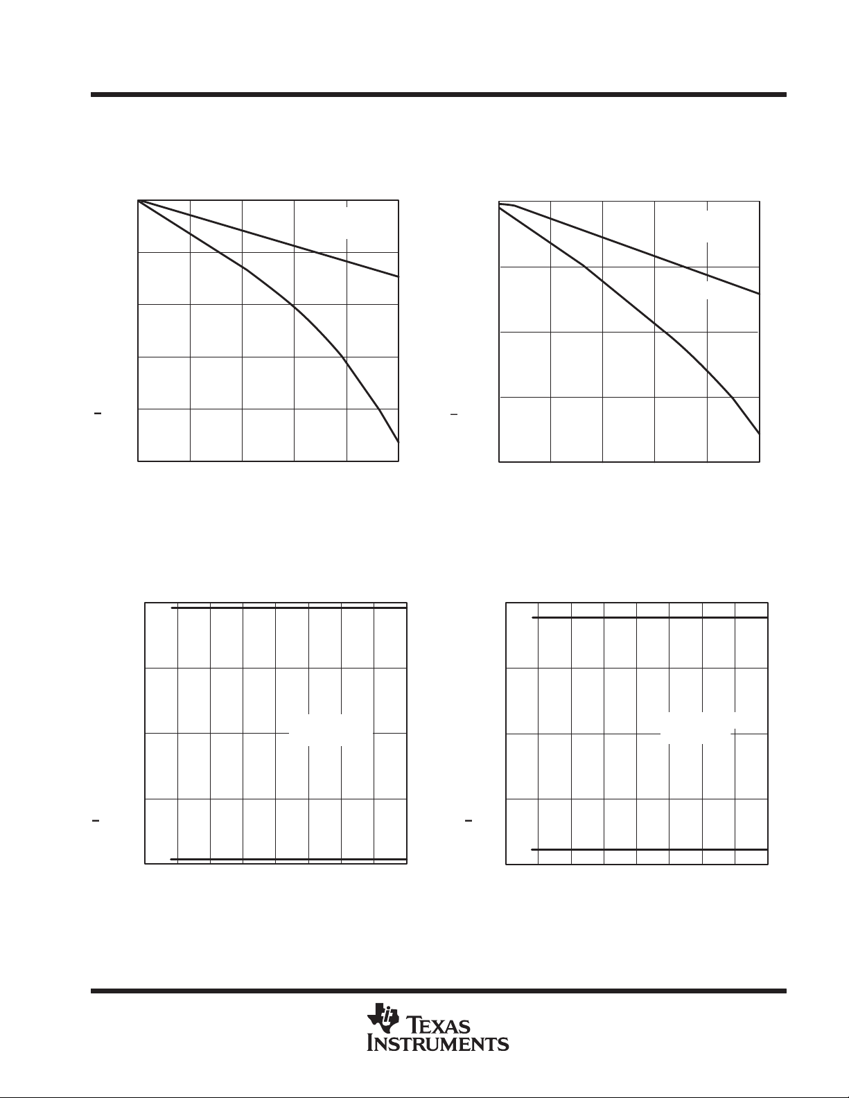
vs Common mode in ut voltage
2
IB
gq y
IIOInput offset current
gq y
VOMMaximum peak output voltage
,
AVDLarge-signal differential voltage amplification
qy
Chopping frequenc
yg
IDDSupply current
yg
IOSShort-circuit output current
yg
SR
Slew rate
yg
Pulse response
g
Gain-bandwidth product
yg
vs Su ly voltage
30
φ
m
g
Advanced LinCMOS PRECISION CHOPPER-STABILIZED
OPERATIONAL AMPLIFIERS
SLOS019C – SEPTEMBER 1988 – REVISED FEBRUARY 1999
TYPICAL CHARACTERISTICS
Table of Graphs
V
IO
I
IB
V
(OPP)
V
N(PP)
V
n
φ
m
Normalized input offset voltage vs Chopping frequency 1
Input bias current
p
Clamp current vs Output voltage 7
Maximum peak-to-peak output voltage vs Frequency 8
p
pp
pp
p
Peak-to-peak equivalent input noise voltage vs Chopping frequency 25, 26
Equivalent input noise voltage vs Frequency 27
Phase margin
Phase shift vs Frequency 13
p
p
y
p
p
vs Common-mode input voltage 2
vs Chopping frequency
vs Free-air temperature 4
vs Chopping frequency 5
vs Free-air temperature 6
vs Output current 9, 10
vs Free-air temperature
vs Frequency 13
vs Free-air temperature 14
vs Supply voltage 15
vs Free-air temperature 16
vs Supply voltage 17
vs Free-air temperature 18
vs Supply voltage 19
vs Free-air temperature 20
vs Supply voltage 21
vs Free-air temperature 22
Small-signal 23
Large-signal 24
vs Supply voltage 28
vs Free-air temperature 29
vs Supply voltage 30
vs Free-air temperature
vs Load capacitance 32
FIGURE
3
11, 12
31
12
POST OFFICE BOX 655303 • DALLAS, TEXAS 75265

TLC2652, TLC2652A, TLC2652Y
Advanced LinCMOS PRECISION CHOPPER-STABILIZED
OPERATIONAL AMPLIFIERS
SLOS019C – SEPTEMBER 1988 – REVISED FEBRUARY 1999
TYPICAL CHARACTERISTICS
NORMALIZED INPUT OFFSET VOLTAGE
vs
CHOPPING FREQUENCY
70
V
= ±5 V
DD±
VIC = 0
60
Vµ
IO
V
VIO – Normalized Input Offset – uV
TA = 25°C
50
40
30
20
10
0
–10
100 1 k 10 k 100 k
Chopping Frequency – Hz
†
INPUT BIAS CURRENT
COMMON-MODE INPUT VOLTAGE
25
V
= ±5 V
DD±
TA = 25°C
20
15
10
IB
I
IIB – Input Bias Current – pA
5
0
–5
–4 –3 –2 –1
VIC – Common-Mode Input Voltage – V
vs
01
2345
Figure 1
INPUT BIAS CURRENT
vs
CHOPPING FREQUENCY
70
V
= ±5 V
DD±
VIC = 0
60
TA = 25°C
50
40
30
20
IB
I
IIB – Input Bias Current – pA
10
0
100 1 k 10 k 100 k
Chopping Frequency – Hz
Figure 2
INPUT BIAS CURRENT
vs
FREE-AIR TEMPERATURE
100
V
= ±5 V
DD±
VO = 0
VIC = 0
10
IB
I
IIB – Input Bias Current – pA
1
25 45 65 105 125
TA – Free-Air Temperature – ° C
85
Figure 3
†
Data at high and low temperatures are applicable only within the rated operating free-air temperature ranges of the various devices.
POST OFFICE BOX 655303 • DALLAS, TEXAS 75265
Figure 4
13

TLC2652, TLC2652A, TLC2652Y
Advanced LinCMOS PRECISION CHOPPER-STABILIZED
OPERATIONAL AMPLIFIERS
SLOS019C – SEPTEMBER 1988 – REVISED FEBRUARY 1999
TYPICAL CHARACTERISTICS
INPUT OFFSET CURRENT
vs
CHOPPING FREQUENCY
25
V
= ±5 V
DD±
VIC = 0
TA = 25°C
20
15
10
IO
IIO – Input Offset Current – pA
I
5
0
100 1 k 10 k 100 k
Chopping Frequency – Hz
†
INPUT OFFSET CURRENT
FREE-AIR TEMPERATURE
10
V
= ±5 V
DD±
VIC = 0
8
6
4
IO
IIO – Input Offset Current – pA
I
2
0
25 45 65 85
TA – Free-Air Temperature – ° C
vs
105 125
100 µA
V
DD±
10 µA
1 µA
100 nA
10 nA
|Clamp Current|
100 pA
10 pA
TA = 25°C
Positive Clamp Current
1 nA
1 pA
4 4.2 4.4 4.6
Figure 5 Figure 6
MAXIMUM PEAK-TO-PEAK OUTPUT
CLAMP CURRENT
vs
OUTPUT VOLTAGE
10
= ±5 V
8
6
4
Negative Clamp Current
4.8 5
|VO| – Output Voltage – V
2
V
DD±
RL = 10 kΩ
O(PP)
0
V
VO(PP) – Maximum Peak-to-Peak Output Voltage – V
100 1 k 10 k 1 M
VOLTAGE
vs
FREQUENCY
TA = –55°C
TA = 125°C
= ±5 V
f – Frequency – Hz
Figure 7
†
Data at high and low temperatures are applicable only within the rated operating free-air temperature ranges of the various devices.
14
POST OFFICE BOX 655303 • DALLAS, TEXAS 75265
Figure 8
TLC2652, TLC2652A, TLC2652Y
Advanced LinCMOS PRECISION CHOPPER-STABILIZED
OPERATIONAL AMPLIFIERS
SLOS019C – SEPTEMBER 1988 – REVISED FEBRUARY 1999
MAXIMUM PEAK OUTPUT VOLTAGE
OUTPUT CURRENT
5
4.8
V
OM+
4.6
4.4
4.2
OM
|V
|VOM| – Maximum Peak Output Voltage – V
4
0 0.4 0.8 1.2
|IO| – Output Current – mA
vs
TYPICAL CHARACTERISTICS
V
= ±5 V
DD±
TA = 25°C
V
1.6 2
OM–
7.5
7.3
7.1
6.9
OM
|V
|VOM| – Maximum Peak Output Voltage – V
6.7
0 0.4 0.8 1.2
†
MAXIMUM PEAK OUTPUT VOLTAGE
vs
OUTPUT CURRENT
V
= ±7.5 V
DD±
TA = 25°C
V
OM+
|IO| – Output Current – mA
V
OM–
1.6 2
MAXIMUM PEAK OUTPUT VOLTAGE
FREE-AIR TEMPERATURE
5
2.5
0
–2.5
OM
V
VOM – Maximum Peak Output Voltage – V
–5
–50 –25
–75 0 25 50
TA – Free-Air Temperature – ° C
Figure 9
vs
V
= ±5 V
DD±
RL = 10 kΩ
75 100 125
Figure 10
MAXIMUM PEAK OUTPUT VOLTAGE
vs
FREE-AIR TEMPERATURE
8
4
V
= ±7.5 V
DD±
0
–4
OM
V
VOM – Maximum Peak Output Voltage – V
–8
–50 –25
–75 0 25 50 75 100 125
TA – Free-Air Temperature – ° C
RL = 10 kΩ
Figure 11
†
Data at high and low temperatures are applicable only within the rated operating free-air temperature ranges of the various devices.
POST OFFICE BOX 655303 • DALLAS, TEXAS 75265
Figure 12
15

TLC2652, TLC2652A, TLC2652Y
Advanced LinCMOS PRECISION CHOPPER-STABILIZED
OPERATIONAL AMPLIFIERS
SLOS019C – SEPTEMBER 1988 – REVISED FEBRUARY 1999
TYPICAL CHARACTERISTICS
LARGE-SIGNAL DIFFERENTIAL VOLTAGE
AMPLIFICATION AND PHASE SHIFT
FREQUENCY
120
100
80
60
40
20
Voltage Amplification – dB
0
VD
A
AVD – Large-Signal Differential
V
RL = 10 kΩ
–20
CL = 100 pF
TA = 25°C
–40
10 100 1 k 10 k 100 k
DD±
Phase Shift
A
= ±5 V
f – Frequency – Hz
VD
vs
†
1 M 10 M
60°
80°
100°
120°
140°
160°
180°
200°
220°
Phase Shift
Figure 13
LARGE-SIGNAL DIFFERENTIAL VOLTAGE
AMPLIFICATION
FREE-AIR TEMPERATURE
155
150
145
Voltage Amplification – dB
VD
140
A
AVD – Large-Signal Differential
135
–50 –25
–75 0 25 50
TA – Free-Air Temperature – ° C
vs
V
= ±7.5 V
DD±
RL = 10 kΩ
VO = ±4 V
75 100 125
Figure 14
†
Data at high and low temperatures are applicable only within the rated operating free-air temperature ranges of the various devices.
16
POST OFFICE BOX 655303 • DALLAS, TEXAS 75265

TLC2652, TLC2652A, TLC2652Y
Advanced LinCMOS PRECISION CHOPPER-STABILIZED
OPERATIONAL AMPLIFIERS
SLOS019C – SEPTEMBER 1988 – REVISED FEBRUARY 1999
CHOPPING FREQUENCY
SUPPLY VOLTAGE
540
520
500
480
460
Chopping Frequency – kHz
440
420
012345
|V
| – Supply Voltage – V
DD±
Figure 15
vs
TYPICAL CHARACTERISTICS
460
T
= 25°C
A
450
440
430
420
Chopping Frequency – kHz
410
400
–75 0 25 50
678
–50 –25
†
CHOPPING FREQUENCY
vs
FREE-AIR TEMPERATURE
V
TA – Free-Air Temperature – ° C
Figure 16
= ±5 V
DD±
75 100 125
SUPPLY CURRENT
vs
SUPPLY VOLTAGE
2
VO = 0
No Load
1.6
1.2
0.8
DD
IDD – Supply Current – mA
I
0.4
0
0235
146
|VDD ±| – Supply Voltage – V
Figure 17
T
= 25°C
A
TA = –55°C
TA = 125°C
78
SUPPLY CURRENT
FREE-AIR TEMPERATURE
2
V
= ±7.5 V
DD±
1.6
1.2
0.8
DD
IDD – Supply Current – mA
I
0.4
0
–75 0 50
V
= ±5 V
DD±
V
= ±2.5 V
DD±
–50 –25
TA – Free-Air Temperature – ° C
Figure 18
vs
25 75
VO = 0
No Load
100 125
†
Data at high and low temperatures are applicable only within the rated operating free-air temperature ranges of the various devices.
POST OFFICE BOX 655303 • DALLAS, TEXAS 75265
17

TLC2652, TLC2652A, TLC2652Y
Advanced LinCMOS PRECISION CHOPPER-STABILIZED
OPERATIONAL AMPLIFIERS
SLOS019C – SEPTEMBER 1988 – REVISED FEBRUARY 1999
SHORT-CIRCUIT OUTPUT CURRENT
vs
SUPPLY VOLTAGE
12
8
4
0
–4
–8
OS
I
IOS – Short-Circuit Output Current – mA
–12
012345
|VDD ±| – Supply Voltage – V
VID = –100 mV
VID = 100 mV
TYPICAL CHARACTERISTICS
SHORT-CIRCUIT OUTPUT CURRENT
VO = 0
TA = 25°C
678
15
V
DD±
VO = 0
10
5
0
–5
–10
OS
I
IOS – Short-Circuit Output Current – mA
–15
–50 –25
–75 0 25 50
†
vs
FREE-AIR TEMPERATURE
= ±5 V
VID = –100 mV
VID = 100 mV
75 100 125
TA – Free-Air Temperature – ° C
4
3
sµ
V/
2
SR – Slew Rate – V?us
1
0
0123 45
Figure 19
SLEW RATE
vs
SUPPLY VOLTAGE
SR–
SR+
|V
| – Supply Voltage – V
DD±
Figure 21
RL = 10 kΩ
CL = 100 pF
TA = 25°C
678
Figure 20
SLEW RATE
FREE-AIR TEMPERATURE
4
SR–
3
sµ
V/
2
SR – Slew Rate – V?us
1
0
–75 0 25 50
–50 –25
SR+
TA – Free-Air Temperature – ° C
Figure 22
vs
V
= ±5 V
DD±
RL = 10 kΩ
CL = 100 pF
75 100 125
†
Data at high and low temperatures are applicable only within the rated operating free-air temperature ranges of the various devices.
18
POST OFFICE BOX 655303 • DALLAS, TEXAS 75265

TLC2652, TLC2652A, TLC2652Y
Advanced LinCMOS PRECISION CHOPPER-STABILIZED
OPERATIONAL AMPLIFIERS
SLOS019C – SEPTEMBER 1988 – REVISED FEBRUARY 1999
TYPICAL CHARACTERISTICS
O
V
VO – Output Voltage – mV
µV
100
75
50
25
–25
–50
–75
–100
1.8
1.6
1.4
VOLTAGE-FOLLOWER
SMALL-SIGNAL
PULSE RESPONSE
V
= ±5 V
DD±
RL = 10 kΩ
0
CL = 100 pF
TA = 25°C
0123
t – Time – µs
4567
Figure 23
PEAK-TO-PEAK INPUT NOISE VOLTAGE
vs
CHOPPING FREQUENCY
V
DD±
RS = 20 Ω
f = 0 to 1 Hz
TA = 25°C
= ±5 V
4
3
2
1
0
–1
O
V
VO – Output Voltage – V
–2
–3
–4
5
µV
4
VOLTAGE-FOLLOWER
LARGE-SIGNAL
PULSE RESPONSE
V
= ±5 V
DD±
RL = 10 kΩ
CL = 100 pF
TA = 25°C
0 5 10 15 20
t – Time – µs
25 30 35 40
Figure 24
PEAK-TO-PEAK INPUT NOISE VOLTAGE
vs
CHOPPING FREQUENCY
V
= ±5 V
DD±
RS = 20 Ω
f = 0 to 1 Hz
TA = 25°C
N(PP)
V
VN(PP) – Peak-to-Peak Input Noise Voltage –uV
1.2
1
0.8
0.6
0.4
0.2
0
0246810
fch – Chopping Frequency – kHz
Figure 25
POST OFFICE BOX 655303 • DALLAS, TEXAS 75265
3
2
1
N(PP)
V
VN(PP) – Peak-to-Peak Input Noise Voltage – uV
0
0246
fch – Chopping Frequency – kHz
Figure 26
810
19

TLC2652, TLC2652A, TLC2652Y
Advanced LinCMOS PRECISION CHOPPER-STABILIZED
OPERATIONAL AMPLIFIERS
SLOS019C – SEPTEMBER 1988 – REVISED FEBRUARY 1999
EQUIVALENT INPUT NOISE VOLTAGE
vs
FREQUENCY
100
nV/ Hz
80
60
40
20
V
= ±5 V
DD±
n
Vn – Equivalent Input Noise Voltage – nV/Hz
V
RS = 20 Ω
TA = 25°C
0
1 10 100 1 k
f – Frequency – Hz
Figure 27 Figure 28
TYPICAL CHARACTERISTICS
2.1
R
= 10 kΩ
L
CL = 100 pF
TA = 25°C
2
1.9
Gain-Bandwidth Product – MHz
1.8
012345
†
GAIN-BANDWIDTH PRODUCT
vs
SUPPLY VOLTAGE
678
|V
| – Supply Voltage – V
CC±
GAIN-BANDWIDTH PRODUCT
FREE-AIR TEMPERATURE
2.6
2.4
2.2
2
1.8
Gain-Bandwidth Product – MHz
1.4
1.2
–75 0 25 50
–25
–50
TA – Free-Air Temperature – ° C
Figure 29
vs
V
= ±5 V
DD±
RL = 10 kΩ
CL = 100 pF
75 100 125
PHASE MARGIN
vs
SUPPLY VOLTAGE
50°
R
= 10 kΩ
L
CL = 100 pF
TA = 25°C
48°
46°
44°
m
φ
om – Phase Margin
42°
40°
0235
|V
| – Supply Voltage – V
CC±
Figure 30
78146
†
Data at high and low temperatures are applicable only within the rated operating free-air temperature ranges of the various devices.
20
POST OFFICE BOX 655303 • DALLAS, TEXAS 75265

TLC2652, TLC2652A, TLC2652Y
Advanced LinCMOS PRECISION CHOPPER-STABILIZED
OPERATIONAL AMPLIFIERS
SLOS019C – SEPTEMBER 1988 – REVISED FEBRUARY 1999
TYPICAL CHARACTERISTICS
PHASE MARGIN
vs
FREE-AIR TEMPERATURE
50°
48°
46°
44°
m
φ
om – Phase Margin
42°
V
= ±5 V
DD±
RL = 10 kΩ
CL = 100 pF
40°
–75 0 50
–50 –25
TA – Free-Air Temperature – ° C
100 12525 75
Figure 31
†
Data at high and low temperatures are applicable only within the rated operating free-air temperature ranges of the various devices.
60°
50°
40°
30°
m
20°
φ
om – Phase Margin
10°
0°
0 200 400 600
†
PHASE MARGIN
vs
LOAD CAPACITANCE
CL – Load Capacitance – pF
Figure 32
V
= ±5 V
DD±
RL = 10 kΩ
TA = 25°C
800 1000
APPLICATION INFORMATION
capacitor selection and placement
The two important factors to consider when selecting external capacitors CXA and CXB are leakage and
dielectric absorption. Both factors can cause system degradation, negating the performance advantages
realized by using the TLC2652.
Degradation from capacitor leakage becomes more apparent with the increasing temperatures. Low-leakage
capacitors and standoffs are recommended for operation at T
recommended around the capacitor connections on both sides of the printed circuit board to alleviate problems
caused by surface leakage on circuit boards.
Capacitors with high dielectric absorption tend to take several seconds to settle upon application of power, which
directly affects input offset voltage. In applications where fast settling of input offset voltage is needed, it is
recommended that high-quality film capacitors, such as mylar, polystyrene, or polypropylene, be used. In other
applications, however, a ceramic or other low-grade capacitor can suffice.
Unlike many choppers available today , the TLC2652 is designed to function with values of C
range of 0.1 µF to 1 µF without degradation to input offset voltage or input noise voltage. These capacitors
should be located as close as possible to the C
many choppers, connecting these capacitors to V
XA
and C
DD–
pins and returned to either V
XB
causes degradation in noise performance. This problem
is eliminated on the TLC2652.
= 125°C. In addition, guard bands are
A
and CXB in the
XA
or C RETURN. On
DD–
POST OFFICE BOX 655303 • DALLAS, TEXAS 75265
21

TLC2652, TLC2652A, TLC2652Y
Advanced LinCMOS PRECISION CHOPPER-STABILIZED
OPERATIONAL AMPLIFIERS
SLOS019C – SEPTEMBER 1988 – REVISED FEBRUARY 1999
APPLICATION INFORMATION
internal/external clock
The TLC2652 has an internal clock that sets the chopping frequency to a nominal value of 450 Hz. On 8-pin
packages, the chopping frequency can only be controlled by the internal clock; however, on all 14-pin packages
and the 20-pin FK package, the device chopping frequency can be set by the internal clock or controlled
externally by use of the INT/EXT
If external clocking is desired, connect INT/EXT
trip point is 2.5 V above the negative rail; however, CLK IN can be driven from the negative rail to 5 V above
the negative rail. If this level is exceeded, damage could occur to the device unless the current into CLK IN is
limited to ±5 mA. When operating in the single-supply configuration, this feature allows the TLC2652 to be driven
directly by 5-V TTL and CMOS logic. A
divide-by-two frequency divider interfaces with
CLK IN and sets the clock chopping frequency.
The duty cycle of the external is not critical but
should be kept between 30% and 60%.
overload recovery/output clamp
When large differential input voltage conditions
are applied to the TLC2652, the nulling loop
attempts to prevent the output from saturating by
driving C
levels. Once the overdrive condition is removed,
a period of time is required to allow the built-up
charge to dissipate. This time period is defined as
overload recovery time (see Figure 33). Typical
overload recovery time for the TLC2652 is
significantly faster than competitive products;
however, if required, this time can be reduced
further by use of internal clamp circuitry
accessible through CLAMP if required.
and CXB to internally-clamped voltage
XA
and CLK IN pins. T o use the internal 450-Hz clock, no connection is necessary .
to V
and the external clock to CLK IN. The external clock
DD–
0
V
= ±5 V
DD±
TA = 25°C
–5
O
V
0
I
–50
VI – Input Voltage – mV VO – Output Voltage – V
V
0 10203040
t – Time – ms
50 60 70 80
Figure 33. Overload Recovery
The clamp is a switch that is automatically activated when the output is approximately 1 V from either supply
rail. When connected to the inverting input (in parallel with the closed-loop feedback resistor), the closed-loop
gain is reduced, and the TLC2652 output is prevented from going into saturation. Since the output must source
sink current through the switch (see Figure 7), the maximum output voltage swing is slightly reduced.
thermoelectric effects
To take advantage of the extremely low offset voltage drift of the TLC2652, care must be taken to compensate
for the thermoelectric effects present when two dissimilar metals are brought into contact with each other (such
as device leads being soldered to a printed circuit board). Dissimilar metal junctions can produce thermoelectric
voltages in the range of several microvolts per degree Celsius (orders of magnitude greater than the 0.01-µV/°C
typical of the TLC2652).
To help minimize thermoelectric effects, careful attention should be paid to component selection and
circuit-board layout. Avoid the use of nonsoldered connections (such as sockets, relays, switches, etc.) in the
input signal path. Cancel thermoelectric effects by duplicating the number of components and junctions in each
device input. The use of low-thermoelectric-coefficient components, such as wire-wound resistors, is also
beneficial.
22
POST OFFICE BOX 655303 • DALLAS, TEXAS 75265

TLC2652, TLC2652A, TLC2652Y
Advanced LinCMOS PRECISION CHOPPER-STABILIZED
OPERATIONAL AMPLIFIERS
SLOS019C – SEPTEMBER 1988 – REVISED FEBRUARY 1999
APPLICATION INFORMATION
latch-up avoidance
Because CMOS devices are susceptible to latch-up due to their inherent parasitic thyristors, the TLC2652 inputs
and output are designed to withstand –100-mA surge currents without sustaining latch-up; however, techniques
to reduce the chance of latch-up should be used whenever possible. Internal protection diodes should not, by
design, be forward biased. Applied input and output voltages should not exceed the supply voltage by more than
300 mV. Care should be exercised when using capacitive coupling on pulse generators. Supply transients
should be shunted by the use of decoupling capacitors (0.1 µF typical) located across the supply rails as close
to the device as possible.
The current path established if latch-up occurs is usually between the supply rails and is limited only by the
impedance of the power supply and the forward resistance of the parasitic thyristor. The chance of latch-up
occurring increases with increasing temperature and supply voltage.
electrostatic discharge protection
The TLC2652 incorporates internal ESD-protection circuits that prevent functional failures at voltages at or
below 2000 V. Care should be exercised in handling these devices, as exposure to ESD may result in
degradation of the device parametric performance.
theory of operation
Chopper-stabilized operational amplifiers offer the best dc performance of any monolithic operational amplifier .
This superior performance is the result of using two operational amplifiers, a main amplifier and a nulling
amplifier, plus oscillator-controlled logic and two external capacitors to create a system that behaves as a single
amplifier. With this approach, the TLC2652 achieves submicrovolt input offset voltage, submicrovolt noise
voltage, and offset voltage variations with temperature in the nV/°C range.
The TLC2652 on-chip control logic produces two dominant clock phases: a nulling phase and an amplifying
phase. The term chopper-stabilized derives from the process of switching between these two clock phases.
Figure 34 shows a simplified block diagram of the TLC2652. Switches A and B are make-before-break types.
During the nulling phase, switch A is closed shorting the nulling amplifier inputs together and allowing the nulling
amplifier to reduce its own input offset voltage by feeding its output signal back to an inverting input node.
Simultaneously , external capacitor C
remain nulled during the amplifying phase.
IN+
IN–
stores the nulling potential to allow the offset voltage of the amplifier to
XA
Main Amplifier
B
A
Null
Amplifier
+
–
C
B
+
–
A
XB
C
XA
V
O
V
DD–
Figure 34. TLC2652 Simplified Block Diagram
POST OFFICE BOX 655303 • DALLAS, TEXAS 75265
23

TLC2652, TLC2652A, TLC2652Y
Advanced LinCMOS PRECISION CHOPPER-STABILIZED
OPERATIONAL AMPLIFIERS
SLOS019C – SEPTEMBER 1988 – REVISED FEBRUARY 1999
APPLICATION INFORMATION
theory of operation (continued)
During the amplifying phase, switch B is closed connecting the output of the nulling amplifier to a noninverting
input of the main amplifier. In this configuration, the input offset voltage of the main amplifier is nulled. Also,
external capacitor C
nulled during the next nulling phase.
This continuous chopping process allows offset voltage nulling during variations in time and temperature over
the common-mode input voltage range and power supply range. In addition, because the low-frequency signal
path is through both the null and main amplifiers, extremely high gain is achieved.
The low-frequency noise of a chopper amplifier depends on the magnitude of the component noise prior to
chopping and the capability of the circuit to reduce this noise while chopping. The use of the Advanced LinCMOS
process, with its low-noise analog MOS transistors and patent-pending input stage design, significantly reduces
the input noise voltage.
The primary source of nonideal operation in chopper-stabilized amplifiers is error charge from the switches. As
charge imbalance accumulates on critical nodes, input offset voltage can increase, especially with increasing
chopping frequency. This problem has been significantly reduced in the TLC2652 by use of a patent-pending
compensation circuit and the Advanced LinCMOS process.
stores the nulling potential to allow the offset voltage of the main amplifier to remain
XB
The TLC2652 incorporates a feed-forward design that ensures continuous frequency response. Essentially , the
gain magnitude of the nulling amplifier and compensation network crosses unity at the break frequency of the
main amplifier. As a result, the high-frequency response of the system is the same as the frequency response
of the main amplifier. This approach also ensures that the slewing characteristics remain the same during both
the nulling and amplifying phases.
24
POST OFFICE BOX 655303 • DALLAS, TEXAS 75265

TLC2652, TLC2652A, TLC2652Y
Advanced LinCMOS PRECISION CHOPPER-STABILIZED
OPERATIONAL AMPLIFIERS
SLOS019C – SEPTEMBER 1988 – REVISED FEBRUARY 1999
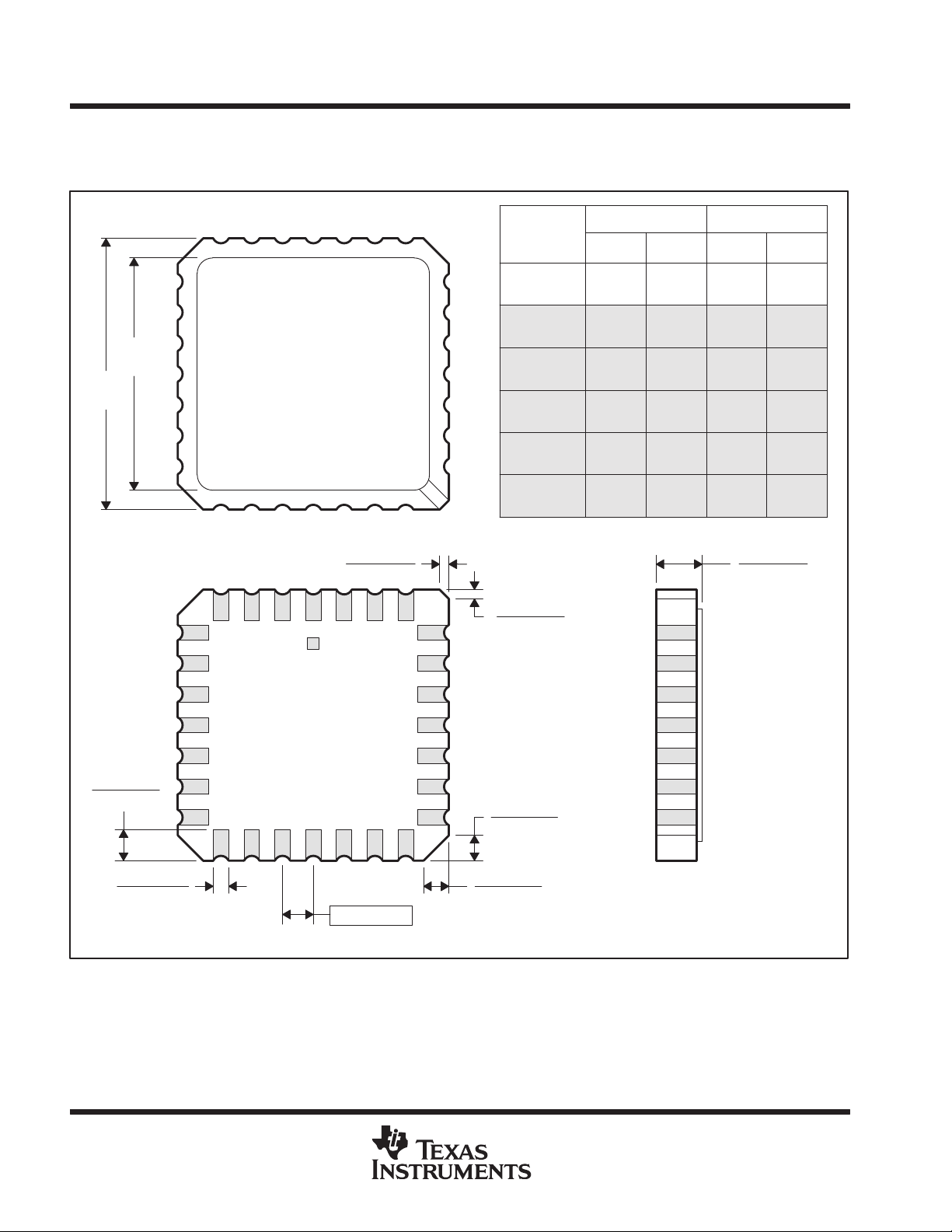
MECHANICAL DATA
D (R-PDSO-G**) PLASTIC SMALL-OUTLINE PACKAGE
14 PIN SHOWN
0.050 (1,27)
14
1
0.069 (1,75) MAX
A
0.020 (0,51)
0.014 (0,35)
0.010 (0,25)
0.004 (0,10)
DIM
8
7
PINS **
0.010 (0,25)
0.157 (4,00)
0.150 (3,81)
M
0.244 (6,20)
0.228 (5,80)
Seating Plane
0.004 (0,10)
8
14
0.008 (0,20) NOM
0°–8°
16
Gage Plane
0.010 (0,25)
0.044 (1,12)
0.016 (0,40)
A MAX
A MIN
NOTES: A. All linear dimensions are in inches (millimeters).
B. This drawing is subject to change without notice.
C. Body dimensions do not include mold flash or protrusion, not to exceed 0.006 (0,15).
D. Falls within JEDEC MS-012
POST OFFICE BOX 655303 • DALLAS, TEXAS 75265
0.197
(5,00)
0.189
(4,80)
0.344
(8,75)
0.337
(8,55)
0.394
(10,00)
0.386
(9,80)
4040047/D 10/96
25
TLC2652, TLC2652A, TLC2652Y
Advanced LinCMOS PRECISION CHOPPER-STABILIZED
OPERATIONAL AMPLIFIERS
SLOS019C – SEPTEMBER 1988 – REVISED FEBRUARY 1999
MECHANICAL DATA
FK (S-CQCC-N**) LEADLESS CERAMIC CHIP CARRIER
28 TERMINAL SHOWN
A SQ
B SQ
24
19
20
21
22
23
25
12826 27
121314151618 17
0.020 (0,51)
0.010 (0,25)
MIN
0.342
(8,69)
0.442
0.640
0.739
0.938
1.141
A
0.358
(9,09)
0.458
(11,63)
0.660
(16,76)
0.761
(19,32)(18,78)
0.962
(24,43)
1.165
(29,59)
NO. OF
TERMINALS
**
11
10
9
8
7
6
5
432
20
28
44
52
68
84
0.020 (0,51)
0.010 (0,25)
(11,23)
(16,26)
(23,83)
(28,99)
MINMAX
0.307
(7,80)
0.406
(10,31)
0.495
(12,58)
0.495
(12,58)
0.850
(21,6)
1.047
(26,6)
0.080 (2,03)
0.064 (1,63)
B
MAX
0.358
(9,09)
0.458
(11,63)
0.560
(14,22)
0.560
(14,22)
0.858
(21,8)
1.063
(27,0)
0.055 (1,40)
0.045 (1,14)
0.028 (0,71)
0.022 (0,54)
0.050 (1,27)
NOTES: A. All linear dimensions are in inches (millimeters).
26
B. This drawing is subject to change without notice.
C. This package can be hermetically sealed with a metal lid.
D. The terminals are gold plated.
E. Falls within JEDEC MS-004
POST OFFICE BOX 655303 • DALLAS, TEXAS 75265
0.045 (1,14)
0.035 (0,89)
0.045 (1,14)
0.035 (0,89)
4040140/D 10/96
TLC2652, TLC2652A, TLC2652Y
Advanced LinCMOS PRECISION CHOPPER-STABILIZED
OPERATIONAL AMPLIFIERS
SLOS019C – SEPTEMBER 1988 – REVISED FEBRUARY 1999
MECHANICAL DATA
J (R-GDIP-T**) CERAMIC DUAL-IN-LINE PACKAGE
14 PIN SHOWN
14
1
0.065 (1,65)
0.045 (1,14)
0.100 (2,54)
0.070 (1,78)
PINS **
DIM
A MAX
B
8
C
7
0.020 (0,51) MIN
0.200 (5,08) MAX
A MIN
B MAX
B MIN
C MAX
C MIN
Seating Plane
0.310
(7,87)
0.290
(7,37)
0.785
(19,94)
0.755
(19,18)
0.300A0.300
(7,62)
0.245
(6,22)
0.310
(7,87)
0.290
(7,37)
0.785
(19,94)
0.755
(19,18)
(7,62)
0.245
(6,22)
181614
0.310
(7,87)
0.290
(7,37)
0.910
(23,10)
0.300
(7,62)
0.245
(6,22)
20
0.310
(7,87)
0.290
(7,37)
0.975
(24,77)
0.930
(23,62)
0.300
(7,62)
0.245
(6,22)
0.100 (2,54)
0.023 (0,58)
0.015 (0,38)
NOTES: A. All linear dimensions are in inches (millimeters).
B. This drawing is subject to change without notice.
C. This package can be hermetically sealed with a ceramic lid using glass frit.
D. Index point is provided on cap for terminal identification only on press ceramic glass frit seal only.
E. Falls within MIL STD 1835 GDIP1-T14, GDIP1-T16, GDIP1-T18, GDIP1-T20, and GDIP1-T22.
0.130 (3,30) MIN
0°–15°
0.014 (0,36)
0.008 (0,20)
4040083/D 08/98
POST OFFICE BOX 655303 • DALLAS, TEXAS 75265
27

TLC2652, TLC2652A, TLC2652Y
Advanced LinCMOS PRECISION CHOPPER-STABILIZED
OPERATIONAL AMPLIFIERS
SLOS019C – SEPTEMBER 1988 – REVISED FEBRUARY 1999
MECHANICAL DATA
JG (R-GDIP-T8) CERAMIC DUAL-IN-LINE PACKAGE
0.400 (10,20)
0.355 (9,00)
0.063 (1,60)
0.015 (0,38)
0.100 (2,54)
8
1
5
4
0.065 (1,65)
0.045 (1,14)
0.020 (0,51) MIN
0.280 (7,11)
0.245 (6,22)
0.200 (5,08) MAX
0.130 (3,30) MIN
0.023 (0,58)
0.015 (0,38)
0.310 (7,87)
0.290 (7,37)
Seating Plane
0°–15°
0.014 (0,36)
0.008 (0,20)
NOTES: A. All linear dimensions are in inches (millimeters).
28
B. This drawing is subject to change without notice.
C. This package can be hermetically sealed with a ceramic lid using glass frit.
D. Index point is provided on cap for terminal identification only on press ceramic glass frit seal only.
E. Falls within MIL-STD-1835 GDIP1-T8
POST OFFICE BOX 655303 • DALLAS, TEXAS 75265
4040107/C 08/96
TLC2652, TLC2652A, TLC2652Y
Advanced LinCMOS PRECISION CHOPPER-STABILIZED
OPERATIONAL AMPLIFIERS
SLOS019C – SEPTEMBER 1988 – REVISED FEBRUARY 1999
MECHANICAL DATA
N (R-PDIP-T**) PLASTIC DUAL-IN-LINE PACKAGE
16 PIN SHOWN
16
1
0.035 (0,89) MAX
PINS **
DIM
A
9
0.260 (6,60)
0.240 (6,10)
8
0.070 (1,78) MAX
0.020 (0,51) MIN
0.200 (5,08) MAX
A MAX
A MIN
Seating Plane
14
0.775
(19,69)
0.745
(18,92)
16
0.775
(19,69)
0.745
(18,92)
18
0.920
(23.37)
0.850
(21.59)
20
0.975
(24,77)
0.940
(23,88)
0.310 (7,87)
0.290 (7,37)
0.100 (2,54)
0.021 (0,53)
0.015 (0,38)
NOTES: A. All linear dimensions are in inches (millimeters).
B. This drawing is subject to change without notice.
C. Falls within JEDEC MS-001 (20 pin package is shorter then MS-001.)
0.010 (0,25)
M
0.125 (3,18) MIN
0°–15°
0.010 (0,25) NOM
14/18 PIN ONL Y
4040049/C 08/95
POST OFFICE BOX 655303 • DALLAS, TEXAS 75265
29
TLC2652, TLC2652A, TLC2652Y
Advanced LinCMOS PRECISION CHOPPER-STABILIZED
OPERATIONAL AMPLIFIERS
SLOS019C – SEPTEMBER 1988 – REVISED FEBRUARY 1999
MECHANICAL DATA
P (R-PDIP-T8) PLASTIC DUAL-IN-LINE PACKAGE
0.400 (10,60)
0.355 (9,02)
58
0.260 (6,60)
0.240 (6,10)
41
0.070 (1,78) MAX
0.020 (0,51) MIN
0.200 (5,08) MAX
0.125 (3,18) MIN
0.100 (2,54)
0.021 (0,53)
0.015 (0,38)
NOTES: A. All linear dimensions are in inches (millimeters).
B. This drawing is subject to change without notice.
C. Falls within JEDEC MS-001
0.010 (0,25)
M
0.310 (7,87)
0.290 (7,37)
Seating Plane
0°–15°
0.010 (0,25) NOM
4040082/B 03/95
30
POST OFFICE BOX 655303 • DALLAS, TEXAS 75265

IMPORTANT NOTICE
T exas Instruments and its subsidiaries (TI) reserve the right to make changes to their products or to discontinue
any product or service without notice, and advise customers to obtain the latest version of relevant information
to verify, before placing orders, that information being relied on is current and complete. All products are sold
subject to the terms and conditions of sale supplied at the time of order acknowledgement, including those
pertaining to warranty, patent infringement, and limitation of liability.
TI warrants performance of its semiconductor products to the specifications applicable at the time of sale in
accordance with TI’s standard warranty. Testing and other quality control techniques are utilized to the extent
TI deems necessary to support this warranty . Specific testing of all parameters of each device is not necessarily
performed, except those mandated by government requirements.
CERT AIN APPLICATIONS USING SEMICONDUCTOR PRODUCTS MAY INVOLVE POTENTIAL RISKS OF
DEATH, PERSONAL INJURY, OR SEVERE PROPERTY OR ENVIRONMENTAL DAMAGE (“CRITICAL
APPLICATIONS”). TI SEMICONDUCTOR PRODUCTS ARE NOT DESIGNED, AUTHORIZED, OR
WARRANTED TO BE SUITABLE FOR USE IN LIFE-SUPPORT DEVICES OR SYSTEMS OR OTHER
CRITICAL APPLICA TIONS. INCLUSION OF TI PRODUCTS IN SUCH APPLICATIONS IS UNDERST OOD TO
BE FULLY AT THE CUSTOMER’S RISK.
In order to minimize risks associated with the customer’s applications, adequate design and operating
safeguards must be provided by the customer to minimize inherent or procedural hazards.
TI assumes no liability for applications assistance or customer product design. TI does not warrant or represent
that any license, either express or implied, is granted under any patent right, copyright, mask work right, or other
intellectual property right of TI covering or relating to any combination, machine, or process in which such
semiconductor products or services might be or are used. TI’s publication of information regarding any third
party’s products or services does not constitute TI’s approval, warranty or endorsement thereof.
Copyright 1999, Texas Instruments Incorporated
 Loading...