

Texas Instruments TLC2555IDR, TLC2552IDR, TLC2552IDGKR, TLC2552IDGK, TLC2552ID Datasheet
...
TLC2551, TLC2552, TLC2555
5 V, LOW POWER, 12-BIT, 400 KSPS,
SERIAL ANALOG-TO-DIGITAL CONVERTERS WITH AUTOPOWER DOWN
SLAS276 –MARCH 2000
1
POST OFFICE BOX 655303 • DALLAS, TEXAS 75265
D
Maximum Throughput . . . 400 KSPS
D
INL/DNL: ±1 LSB Max, SINAD: 72 dB,
fi = 20 kHz, SFDR: 85 dB, fi = 20 kHz
D
SPI/DSP-Compatible Serial Interfaces With
SCLK up to 20 MHz
D
Single 5 V Supply
D
Rail-to-Rail Analog Input With 500 kHz BW
D
Three Options Available:
– TLC2551 – Single Channel Input
– TLC2552 – Dual Channels With
Autosweep
– TLC2555 – Single Channel With
Pseudo-Differential Input
D
Optimized DSP Mode – Requires FS Only
D
Low Power With Autopower Down
– Operating Current : 3.5 mA
Autopower Down: 8 µA
D
Small 8-Pin MSOP and SOIC Packages
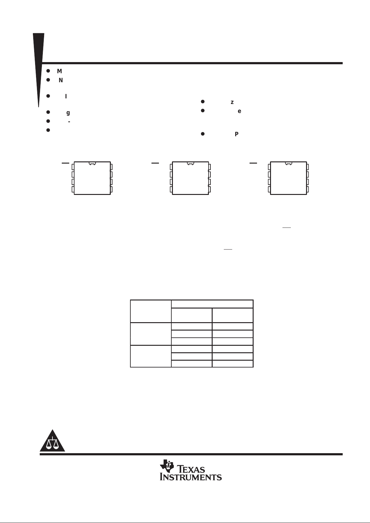
PACKAGE TOP VIEW
TLC2551
1
2
3
4
8
7
6
5
CS
V
REF
GND
AIN
SDO
FS
V
DD
SCLK
1
2
3
4
8
7
6
5
CS/FS
V
REF
GND
AIN0
SDO
SCLK
V
DD
AIN1
TLC2552
1
2
3
4
8
7
6
5
CS/FS
V
REF
GND
AIN(+)
SDO
SCLK
V
DD
AIN(–)
TLC2555
description
The TLC2551/2552/2555 are a family of high performance, 12-bit, low power, miniature 1.5 µs, CMOS
analog-to-digital converters (ADC). The TLC255x family uses a 5 V supply . Devices are available with single,
dual, or single pseudo-differential inputs. The TLC2551 has a 3-state output chip select (CS), serial output clock
(SCLK), and serial data output (SDO) that provides a direct 3-wire interface to the serial port of most popular
host microprocessors (SPI interface). When interfaced with a DSP, a frame sync signal (FS) is used to indicate
the start of a serial data frame. The TLV2552/55 have a shared CS
/FS terminal.
TLC2551/2/5 are designed to operate with very low power consumption. The power saving feature is further
enhanced with an autopower-down mode. This product family features a high-speed serial link to modern host
processors with SCLK up to 20 MHz. TLC255x family uses the SCLK as the conversion clock, thus providing
synchronous operation allowing a minimum conversion time of 1.5 µs using 20 MHz SCLK.
AVAILABLE OPTIONS
PACKAGED DEVICES
T
A
8-MSOP
(DGK)
8-SOIC
(D)
TLC2551CDGK
0°C to 70°C
TLC2552CDGK
TLC2555CDGK
TLC2551IDGK TLC2551ID
–40°C to 85°C
TLC2552IDGK TLC2552ID
TLC2555IDGK TLC2555ID
Copyright 2000, Texas Instruments Incorporated
PRODUCTION DATA information is current as of publication date.
Products conform to specifications per the terms of Texas Instruments
standard warranty. Production processing does not necessarily include
testing of all parameters.
Please be aware that an important notice concerning availability, standard warranty, and use in critical applications of
Texas Instruments semiconductor products and disclaimers thereto appears at the end of this data sheet.
TLC2551, TLC2552, TLC2555
5 V, LOW POWER, 12-BIT, 400 KSPS,
SERIAL ANALOG-TO-DIGITAL CONVERTERS WITH AUTOPOWER DOWN
SLAS276 –MARCH 2000
2
POST OFFICE BOX 655303 • DALLAS, TEXAS 75265
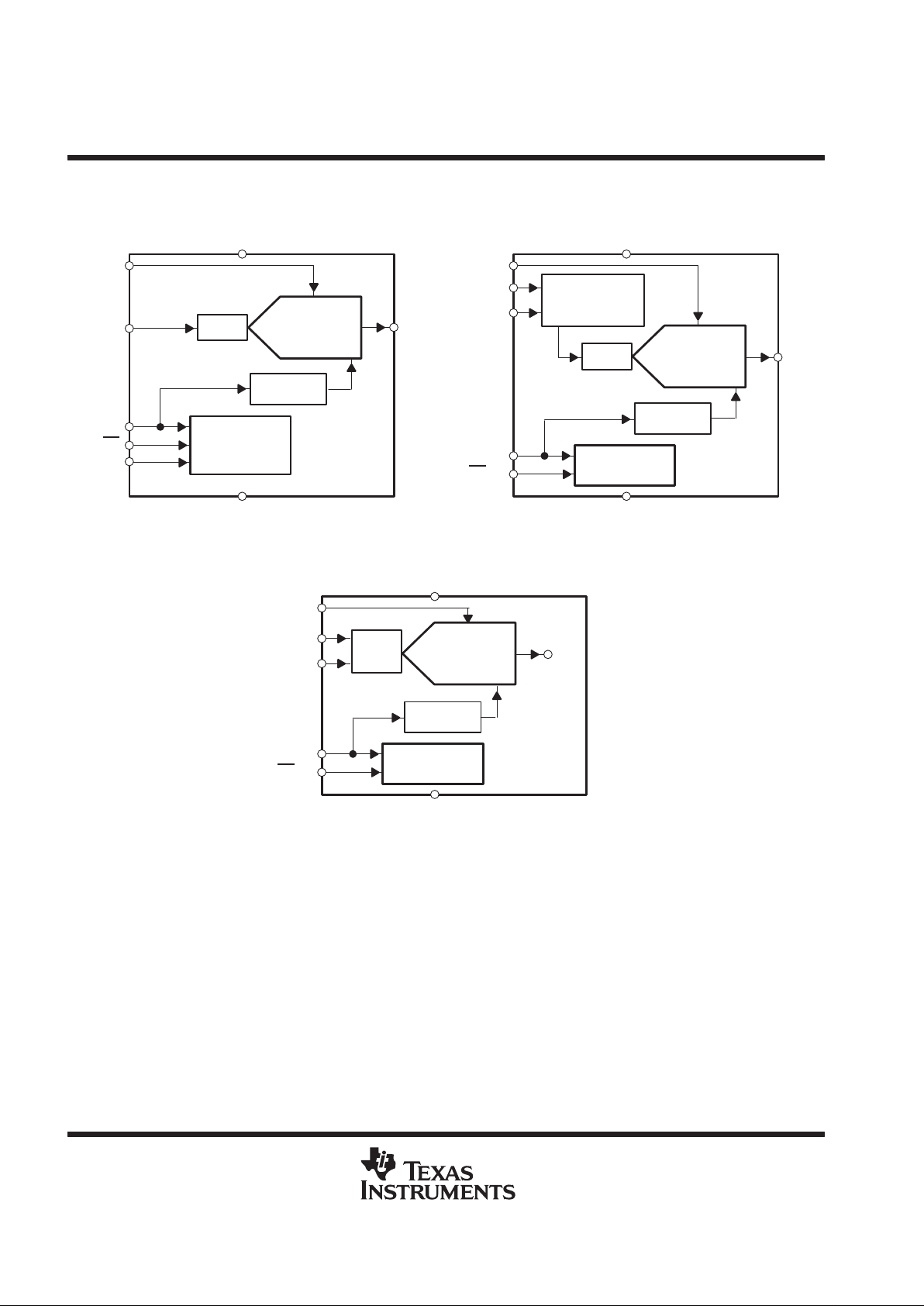
functional block diagram
S/H
SDO
REF
LOW POWER
SAR ADC
V
DD
Conversion
Clock
CONTROL
LOGIC
Mux
S/H
LOW POWER
12-BIT
SAR ADC
Conversion
Clock
CONTROL
LOGIC
AIN
SCLK
CS
FS
REF
AIN0
AIN1
SCLK
CS
/FS
SDO
V
DD
GNDGND
TLC2551 TLC2552
S/H
LOW POWER
12-BIT
SAR ADC
Conversion
Clock
CONTROL
LOGIC
REF
AIN (+)
AIN (–)
SCLK
CS
/FS
SDO
V
DD
GND
TLC2555
TLC2551, TLC2552, TLC2555
5 V, LOW POWER, 12-BIT, 400 KSPS,
SERIAL ANALOG-TO-DIGITAL CONVERTERS WITH AUTOPOWER DOWN
SLAS276 –MARCH 2000
3
POST OFFICE BOX 655303 • DALLAS, TEXAS 75265
Terminal Functions
TLC2551
TERMINAL
NAME NO.
I/O
DESCRIPTION
AIN 4 I Analog input channel
CS 1 I Chip select. A high-to-low transition on the CS input removes SDO from 3-state within a maximum setup time.
CS
can be used as the FS pin when a dedicated serial port is used. If TLC2551 is attached to a dedicated DSP serial
port, this terminal can be grounded.
FS 7 I DSP frame sync input. Indication of the start of a serial data frame. Tie this terminal to VDD if not used.
GND 3 I Ground return for the internal circuitry . Unless otherwise noted, all voltage measurements are with respect to GND.
SCLK 5 I Output serial clock. This terminal receives the serial SCLK from the host processor .
SDO 8 O The 3-state serial output for the A/D conversion result. SDO is kept in the high-impedance state until CS falling edge.
The output format is MSB first.
When FS is not used (FS = 1 at the falling edge of CS): The MSB is presented to the SDO pin after CS falling edge
and output data is valid on the falling edge of SCLK.
When FS is used (FS = 0 at the falling edge of CS
): The MSB is presented to the SDO pin after the falling edge of
FS or the falling edge of CS
(whichever happens first). Output data is valid on the falling edge of SCLK. (This is
typically used with an active FS from a DSP).
V
DD
6 I Positive supply voltage
V
REF
2 I External reference input
TLC2552/55
TERMINAL
NAME NO.
I/O
DESCRIPTION
AIN0 /AIN(+) 4 I Analog input channel 0. (positive input for TL V2555)
AIN1/AIN (–) 5 I Analog input channel 1 (inverted input for TLV2555)
CS/FS 1 I Chip select/frame sync. A high-to-low transition on the CS/FS removes SDO from 3-state within a maximum delay
time.
GND 3 I Ground return for the internal circuitry . Unless otherwise noted, all voltage measurements are with respect to GND.
SCLK 7 I Output serial clock. This terminal receives the serial SCLK from the host processor .
SDO 8 O The 3-state serial output for the A/D conversion result. SDO is kept in the high-impedance state when CS/FS is
high and presents output data after the CS
/FS falling edge until the LSB is presented. The output format is MSB
first. SDO returns to the Hi-Z state after the 16th SCLK. Output data is valid on the falling SCLK edge.
V
DD
6 I Positive supply voltage
V
REF
2 I External reference input
detailed description
The TLC2551/2/5 are successive approximation (SAR) ADCs utilizing a charge redistribution DAC. Figure 1
shows a simplified version of the ADC.
The sampling capacitor acquires the signal on AIN during the sampling period. When the conversion process
starts, the SAR control logic and charge redistribution DAC are used to add and subtract fixed amounts of charge
from the sampling capacitor to bring the comparator into a balanced condition. When the comparator is
balanced, the conversion is complete and the ADC output code is generated.

TLC2551, TLC2552, TLC2555
5 V, LOW POWER, 12-BIT, 400 KSPS,
SERIAL ANALOG-TO-DIGITAL CONVERTERS WITH AUTOPOWER DOWN
SLAS276 –MARCH 2000
4
POST OFFICE BOX 655303 • DALLAS, TEXAS 75265
detailed description (continued)
GND/AIN(–)
ADC Code
AIN
Charge
Redistribution
DAC
Control
Logic
_
+
Figure 1. Simplified SAR Circuit
serial interface
OUTPUT DATA FORMAT
MSB LSB
D15–D4 D3–D0
Conversion result (OD11–OD0) Don’t care
The output data format is binary (unipolar straight binary).
binary
Zero scale code = 000h, Vcode = GND
Full scale code = FFFh, Vcode = VREFP – 1 LSB
pseudo-differential inputs
The TLC2555 operates in pseudo-differential mode. The inverted input is available on terminal 5. It can have
a maximum input ripple of ±0.2 V. This is normally used for ground noise rejection.
control and timing
start of the cycle
TLC2551
D
When FS is not used ( FS = 1 at the falling edge of CS), the falling edge of CS is the start of the cycle. Output
data changes on the rising edge of SCLK. This is typically used for a microcontroller with SPI interface,
although it can also be used for a DSP. The microcontroller SPI interface should be programmed for
CPOL=0 (serial clock reference to ground) and CPHA=1 (data is valid on the falling edge of serial clock).
D
When FS is used ( FS is an active signal from a DSP), the falling edge of FS is the start of the cycle. Output
data changes on the rising edge of SCLK. This is typically used for a TMS320 DSP. If the TLC2551 is
attached to a dedicated DSP serial port. CS terminal can be grounded.
TLC2552/5
The CS
and FS inputs are accessed via the same pin (pin 1) on the TLC2552 and TLC2555. The cycle is started
by the falling edge transition provided by either a CS (interfacing with a SPI interface microcontroller) signal or
FS (interfacing with a TMS320 DSP) signal. Timing for the TLC2555 is much like the TLC2551, with the
exception of the CS
/FS line.

TLC2551, TLC2552, TLC2555
5 V, LOW POWER, 12-BIT, 400 KSPS,
SERIAL ANALOG-TO-DIGITAL CONVERTERS WITH AUTOPOWER DOWN
SLAS276 –MARCH 2000
5
POST OFFICE BOX 655303 • DALLAS, TEXAS 75265
detailed description (continued)
TLC2552 channel MUX reset cycle
The TLC2552 uses CS/FS to reset the AIN multiplexer. A short active CS/FS cycle (4–7 SCLKs) resets the MUX
to AIN0. If the CS
/FS cycle is sufficient to complete the conversion (16 SCLKs plus maximum conversion time),
the MUX toggles to the next channel (see Figure 4 for timing).
sampling
The converter sample time is 12 SCLKs beginning on the 5th SCLK received after the converter has received
an active CS or FS signal (CS/FS for the TLC2552/5).
conversion
The TLC2551 completes conversion in the following manner. The conversion is started after the 16th SCLK
edge. The conversion takes 1.4 µs using 20 MHz SCLK plus 0.1 µs overhead. Enough time (for conversion)
should be allowed before a rising CS/FS edge so that no conversion is terminated prematurely.
TLC2552 input channel selection is toggled on each rising CS /FS edge. The MUX channel can be reset to AIN0
via CS /FS as described in the earlier section and in Figure 5. The input is sampled for 12 SCLKs, converted,
and the result is presented on SDO during the next cycle. Care should also be taken to allow enough time
between samples to avoid prematurely terminating the conversion, which occurs on a rising CS
/FS transition
if the conversion is not complete.
TLC2551, TLC2552, TLC2555
5 V, LOW POWER, 12-BIT, 400 KSPS,
SERIAL ANALOG-TO-DIGITAL CONVERTERS WITH AUTOPOWER DOWN
SLAS276 –MARCH 2000
6
POST OFFICE BOX 655303 • DALLAS, TEXAS 75265
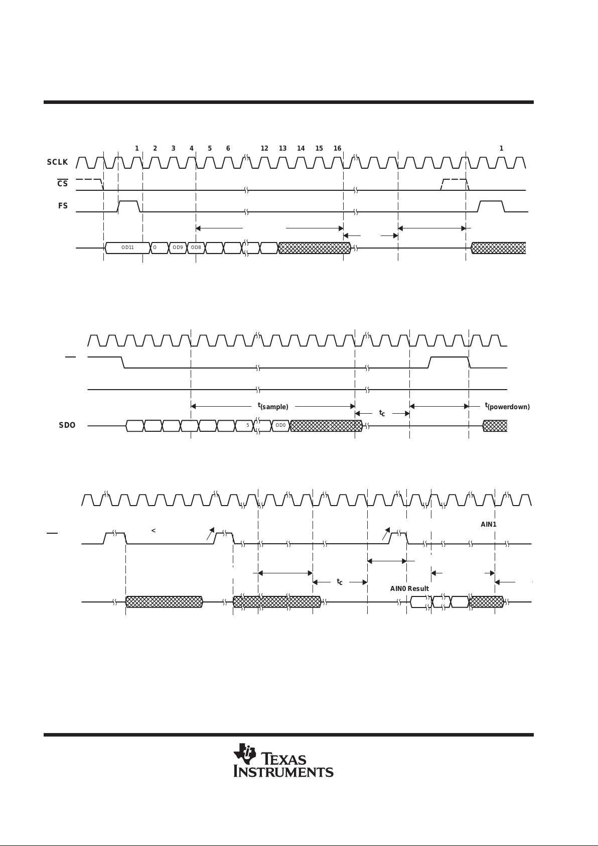
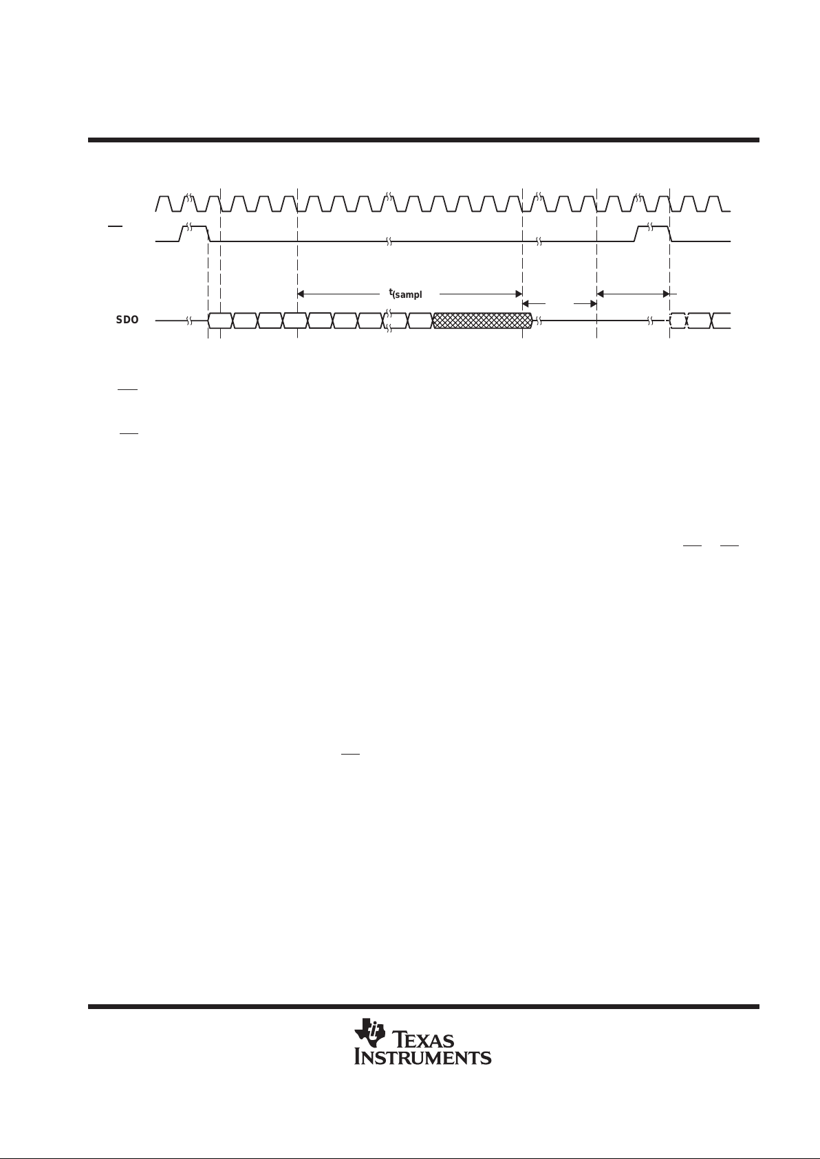
timing diagrams/conversion cycles
DSP Interface
SCLK
1 2 3 4 5 6 12 13 14 15 16 1
CS
FS
OD9 OD8OD11 OD10 OD7 OD6 OD0
SDO
t
(sample)
t
c
t
(powerdown)
Figure 2. TLC2551 DSP Mode/FS Active
µP Interface
SCLK
1 2 3 4 5 6 12 13 14 15 16 1
CS
FS
OD8 OD7 OD6 OD5 OD0
SDO
t
(sample)
t
c
t
(powerdown)
7
OD10OD11 OD9
Figure 3. TLC2551 Microcontroller Mode/(SPI, CPOL = 0, CPHA = 1)
SCLK
2 3 4 5 1 12 16
CS/FS
SDO
t
(powerdown)
t
c
1 4 161241
OD11 OD0
t
(sample)
>8 SCLKs, MUX Toggles to AIN1
AIN0 Result
t
c
<8 SCLKs, MUX
Resets to AIN0
t
(sample)
Figure 4. TLC2552 Timing
TLC2551, TLC2552, TLC2555
5 V, LOW POWER, 12-BIT, 400 KSPS,
SERIAL ANALOG-TO-DIGITAL CONVERTERS WITH AUTOPOWER DOWN
SLAS276 –MARCH 2000
7
POST OFFICE BOX 655303 • DALLAS, TEXAS 75265
timing diagrams/conversion cycles (continued)
OD8
SCLK
1 2 3 4 5 6 12 13 14 15 16
CS/FS
OD7 OD6 OD5 OD0
ООООО
SDO
t
(sample)
t
c
t
(powerdown)
7
OD9
1
OD10 OD9OD11 OD10
OD11
Figure 5. TLC2555 Timing
use CS as FS input
When interfacing the TLC2551 with the TMS320 DSP, the FSR signal from the DSP may be connected to the
CS input if this is the only device on the serial port. This will save one output terminal from the DSP . (Output data
changes on the falling edge of SCLK. Default for TLC2552 and TLC2555).
SCLK and conversion speed
It takes 14 conversion clocks to complete the conversion. The conversion clock for the TLC2551/2/5 is equal
to SCLK/2. This yields a minimum conversion time of 1.4 µs plus 0.1 µs overhead. These devices can operate
with an SCLK up to 20 MHz for the supply voltage range specified. The total conversion time is 14× (1/10M)
+16× (1/20M)+ 0.1 µs} = 2.3 µs for a 20 MHz SCLK. This is the minimum cycle time for an active CS or CS/FS
signal. If violated, the conversion will terminate, invalidating the next data output cycle.
reference voltage
An external reference is applied via VREF. The voltage level applied to this pin establishes the upper limit of
the analog inputs to produce a full-scale reading. The value of V
REF
and the analog input should not exceed
the positive supply or be less than GND, consistent with the specified absolute maximum ratings. The digital
output is at full scale when the input signal is equal to or higher than V
REF
and at zero when the input signal
is equal to or lower than GND.
powerdown and powerup initialization
Autopower down is built in to the devices in order to reduce power consumption. The wake-up time is fast
enough to provide power down between each cycle. The power-down state is initiated at the end of conversion
and wakes up upon a falling edge on CS or FS.

TLC2551, TLC2552, TLC2555
5 V, LOW POWER, 12-BIT, 400 KSPS,
SERIAL ANALOG-TO-DIGITAL CONVERTERS WITH AUTOPOWER DOWN
SLAS276 –MARCH 2000
8
POST OFFICE BOX 655303 • DALLAS, TEXAS 75265
absolute maximum ratings over operating free-air temperature (unless otherwise noted)
†
Supply voltage range, GND to VDD –0.3 V to 6.5 V. . . . . . . . . . . . . . . . . . . . . . . . . . . . . . . . . . . . . . . . . . . . . . . . .
Analog input voltage range –0.3 V to V
DD
+ 0.3 V. . . . . . . . . . . . . . . . . . . . . . . . . . . . . . . . . . . . . . . . . . . . . . . . . . .
Reference input voltage V
DD
+ 0.3 V. . . . . . . . . . . . . . . . . . . . . . . . . . . . . . . . . . . . . . . . . . . . . . . . . . . . . . . . . . . . .
Digital input voltage range –0.3 V to V
DD
+ 0.3 V. . . . . . . . . . . . . . . . . . . . . . . . . . . . . . . . . . . . . . . . . . . . . . . . . . .
Operating virtual junction temperature range, TJ –40°C to 150°C. . . . . . . . . . . . . . . . . . . . . . . . . . . . . . . . . . . . .
Operating free-air temperature range, TA:C 0°C to 70°C. . . . . . . . . . . . . . . . . . . . . . . . . . . . . . . . . . . . . . . . . . .
I –40°C to 85°C. . . . . . . . . . . . . . . . . . . . . . . . . . . . . . . . . . . . . . . . . .
Storage temperature range, T
stg
–65°C to 150°C. . . . . . . . . . . . . . . . . . . . . . . . . . . . . . . . . . . . . . . . . . . . . . . . . . .
Lead temperature 1,6 mm (1/16 inch) from case for 10 seconds 260°C. . . . . . . . . . . . . . . . . . . . . . . . . . . . . . .
†
Stresses beyond those listed under “absolute maximum ratings” may cause permanent damage to the device. These are stress ratings only, and
functional operation of the device at these or any other conditions beyond those indicated under “recommended operating conditions” is not
implied. Exposure to absolute-maximum-rated conditions for extended periods may affect device reliability.
recommended operating conditions
MIN NOM MAX UNIT
Supply voltage, V
DD
2.7 3.3 5.5 V
Positive external reference voltage input, V
REFP
(see Note 1) 2 V
DD
V
Analog input voltage (see Note 1) 0 V
DD
V
High level control input voltage, V
IH
2.1 V
Low-level control input voltage, V
IL
0.6 V
Setup time, CS falling edge (for 2551) or CS/FS falling edge (for
2552/55) before first SCLK falling edge, t
su(CSL-SCLKL)
VDD = REF = 5.5 V 40 ns
Hold time, CS rising edge after SCLK falling edge, t
h(SCLKL-CSH)
5 ns
Delay time, delay from CS falling edge to FS rising edge (t
d(CSL-FSH)
0.5 7 SCLKs
Setup time, FS rising edge before SCLK falling edge, t
su(FSH-SCLKL)
0.35 SCLKs
Hold time, FS hold high after SCLK falling edge, t
h(SCLKL-FSL)
0.65 SCLKs
Pulse width CS high time, t
wH(CS)
100 ns
Pulse width FS high time, t
wH(FS)
0.75 SCLKs
SCLK cycle time, VDD = 5.5–4.5 V , t
c(SCLK)
50 10000 ns
Pulse width low time, t
wL(SCLK)
0.4 0.6 SCLKs
Pulse width high time, t
wH(SCLK)
0.4 0.6 SCLKs
Hold time, hold from end of conversion to CS high, t
h(EOC-CSH)
(EOC is internal, indicates end of
conversion time, tc)
0.1 µs
Active CS/FS cycle time to reset internal MUX to AIN0, reset cycle TLC2552 only 4 7 SCLKs
p
p
TLC2551/2/5C 0 70
°
O erating free-air tem erature, T
A
TLC2551/2/5I –40 85
°C
NOTES: 1. Analog input voltages greater than that applied to VREF convert as all ones (111111111111), while input voltages less than that
applied to GND convert as all zeros(000000000000).
2. This is the time required for the clock input signal to fall from VIH max or to rise from VILmax to VIHmin. In the vicinity of normal room
temperature, the devices function with input clock transition time as slow as 1 µs for remote data-acquisition applications where the
sensor and A/D converter are placed several feet away from the controlling microprocessor.

TLC2551, TLC2552, TLC2555
5 V, LOW POWER, 12-BIT, 400 KSPS,
SERIAL ANALOG-TO-DIGITAL CONVERTERS WITH AUTOPOWER DOWN
SLAS276 –MARCH 2000
9
POST OFFICE BOX 655303 • DALLAS, TEXAS 75265
electrical characteristics over recommended operating free-air temperature range,
VDD = V
REF
= 4.5 V to 5.5 V, SCLK frequency = 20 MHz (unless otherwise noted)
PARAMETER TEST CONDITIONS MIN TYP MAX UNIT
V
OH
High-level output voltage VDD = 5.5 V, IOH = –0.2 mA at 30 pF load 2.4 V
V
OL
Low-level output voltage VDD = 5.5 V, IOL = 0.8 mA at 30 pF load 0.4 V
Off-state output current
VO = V
DD
1 2.5
I
OZ
(high-impedance-state)
VO = 0
CS
=
V
DD
–1 –2.5
µ
A
I
IH
High-level input current VI = V
DD
0.005 2.5 µA
I
IL
Low-level input current VI = 0 V –0.005 2.5 µA
I
CC
Operating supply current CS at 0 V, VDD = 4.5 V ~ 5.5 V 3 3.5 mA
Autopower-down current (0.5 µs inactive)
For all digital inputs,
8
I
CC(AUTOPWDN)
Autopower-down current (5 µs inactive)
0≤ V
I
≤ 0.3 V
or
V
I
≥ V
DD
–
0.3 V
,
SCLK = 0, VDD = 4.5 V to 5.5 V, Ext ref
1
µ
A
Selected analog input channel leakage
Selected channel at V
DD
1
gg
current
Selected channel at 0 V
–1
µ
A
Analog inputs 20 45 50
CiI
nput capacitance
Control Inputs
5 25
p
F
Input on resistance VDD = 5.5 V 500 Ω
Delay time, delay from CS falling edge to
SDO valid, t
d(CSL-SDOV)
VDD = REF = 5.5 V, 30 pF 40 ns
Delay time, delay from FS falling edge to
SDO valid, t
d(FSL-SDOV)
VDD = REF = 5.5 V, 30 pF 1 ns
Delay time, delay from SCLK rising edge
to SDO valid, t
d(SCLKH-SDOV)
VDD = REF = 5.5 V, 30 pF 11 ns
Delay time, delay from 17th SCLK rising
edge to SDO 3-state, t
d(SCLK17H-SDOZ)
VDD = REF = 5.5 V, 30 pF 30 ns
t
c
Conversion time Conversion clock = internal oscillator 28 SCLK
t
(sample)
Sampling time See Note 3 300 ns
Action time ICC start to decrease 0.5 SCLK
Aut
opower down
Wakeup time ICC down to MIN [ICC(AUTOPWDN)] 1 2 ms
Autopower down 0.5 SCLK
†
All typical values are at VDD = 5 V, TA = 25°C.
NOTE 3: Minimal t
(sample)
is given by 0.9 × 50 pF × (RS + 0.5 kΩ), where RS is the source output impedance.

TLC2551, TLC2552, TLC2555
5 V, LOW POWER, 12-BIT, 400 KSPS,
SERIAL ANALOG-TO-DIGITAL CONVERTERS WITH AUTOPOWER DOWN
SLAS276 –MARCH 2000
10
POST OFFICE BOX 655303 • DALLAS, TEXAS 75265
ac specifications (fi = 20 kHz)
PARAMETER TEST CONDITIONS MIN TYP MAX UNIT
SINAD Signal-to-noise ratio + distortion 400 KSPS, VDD = V
REF
= 5 V 70 72 dB
THD T otal harmonic distortion 400 KSPS, VDD = V
REF
= 5 V –84 –80 dB
ENOB Effective number of bits 400 KSPS, VDD = V
REF
= 5 V 11.8 Bits
SFDR Spurious free dynamic range 400 KSPS, VDD = V
REF
= 5 V –84 –80 dB
Analog Input
Full power bandwidth, –3 dB 1 MHz
Full-power bandwidth, –1 dB 500 kHz
external reference specifications
PARAMETER TEST CONDITIONS MIN TYP MAX UNIT
Reference input voltage VDD = =4.5 V ~ 5.5 V V
DD
V
p
p
CS = 1, SCLK = 0 100 MΩ
Reference input impedance
V
DD
= 5.5
V
CS = 0, SCLK = 20 MHz 20 25 kΩ
Reference current VDD = V
REF
= 5.5 V 100 400 µA
p
p
CS = 1, SCLK = 0 5 15
p
Reference input capacitance
V
DD
=
V
REF
= 5.5
V
CS = 0, SCLK = 20 MHz 20 45 50
pF
V
REF
Reference voltage VDD = =4.5 V – 5.5 V V
DD
V
dc specification, V
DD
= V
REF
= 4.5 V to 5.5 V, SCLK frequency = 20 MHz (unless otherwise noted)
PARAMETER TEST CONDITIONS MIN NOM MAX UNIT
INL Integral linearity error (see Note 5) ±0.6 ±1 LSB
DNL Differential linearity error See Note 4 ±0.5 ±1 LSB
TLC2551/52 ±1.5
EOOffset error (see Note 6)
See Note 4
TLC2555 ±2.5
LSB
TLC2551/52 ±2
EGGain error (see Note 6)
See Note 4
TLC2555 ±5
LSB
TLC2551/52 ±2
EtTotal unadjusted error (see Note 7)
See Note 4
TLC2555 ±5
LSB
NOTES: 4. Analog input voltages greater than that applied to REFP convert as all ones (111111111111), while input voltages less than that
applied to REFM convert as all zeros (0000000000).
5. Linear error is the maximum deviation from the best straight line through the A/D transfer characteristics.
6. Zero error is the difference between 000000000000 and the converted output for zero input voltage: full-scale error is the difference
between 111111111111 and the converted output for full-scale input voltage.
7. Total unadjusted error comprises linearity, zero, and full-scale errors.

TLC2551, TLC2552, TLC2555
5 V, LOW POWER, 12-BIT, 400 KSPS,
SERIAL ANALOG-TO-DIGITAL CONVERTERS WITH AUTOPOWER DOWN
SLAS276 –MARCH 2000
11
POST OFFICE BOX 655303 • DALLAS, TEXAS 75265
PARAMETER MEASUREMENT INFORMATION
16
OD0
SCLK
V
IH
CS
OD11
SDO
t
(sample)
t
c
4 12
t
wL(SCLK)
OD8
12
V
IL
t
su(CSL-SCLKL)
t
wH(SCLK)
t
h(EOC-CSH)
t
WH(CS)
t
(powerdown)
FS
t
h(SCLKL-FSL)
t
su(FSH-SCLKL)
t
wh(FS)
t
d(CSL-FSH)
t
d(CSL-SDOV)
t
d(SCLKH-SDOV)
t
d(SCLK17H-SDOZ)
Figure 6. Critical Timing TLC2551 (FS is active)
OD10 OD0
SCLK
1
SDO
t
(sample)
t
c
4 1612
OD9
2
CS
t
d(SCLKH-SDOV)
t
d(CSL-SDOV)
t
d(SCLK17H-SDOZ)
OD11
t
(powerdown)
t
su(CSL–SCLKL)
t
h(EOC–CSH)
Figure 7. Critical Timing TLC2551 (FS = 1)

TLC2551, TLC2552, TLC2555
5 V, LOW POWER, 12-BIT, 400 KSPS,
SERIAL ANALOG-TO-DIGITAL CONVERTERS WITH AUTOPOWER DOWN
SLAS276 –MARCH 2000
12
POST OFFICE BOX 655303 • DALLAS, TEXAS 75265
PARAMETER MEASUREMENT INFORMATION
SCLK
1
CS/FS
SDO
t
(sample)
t
c
t
d(SCLK17H-SDOZ)
1 1 12 164
t
(Reset Cycle)
MUX = AIN0
OD11 OD0
OD11
t
d(CSL-SDOV)
t
h(EOC-CSH)
t
d(CSLKH-SDOV)
t
d(CSL-SDOV)
Figure 8. Critical Timing TLC2552 Reset Cycle
OD11 OD0
SCLK
V
IH
SDO
t
(sample)
t
c
4 1612
t
wL(SCLK)
12
V
IL
t
wH(SCLK)
t
h(EOC-CSH)
t
(powerdown)
CS/FS
t
h(SCLKL-FSL)
t
su(FSH-SCLKL)
t
d(CSL-SDOV)
t
d(SCLKH-SDOV)
t
d(SCLK17H-SDOZ)
OD8
t
wh(FS)
Figure 9. Critical Timing TLC2555 Power-Down Cycle

TLC2551, TLC2552, TLC2555
5 V, LOW POWER, 12-BIT, 400 KSPS,
SERIAL ANALOG-TO-DIGITAL CONVERTERS WITH AUTOPOWER DOWN
SLAS276 –MARCH 2000
13
POST OFFICE BOX 655303 • DALLAS, TEXAS 75265
TYPICAL CHARACTERISTICS
Figure 10
0.6
–40 25
INL – Integral Nonlinearity – LSB
t – Temperature – C
INTEGRAL NONLINEARITY
vs
TEMPERATURE
0.7
90
0.65
°
VDD = REF = 5.5 V
400 KSPS
Figure 11
0.35
0.3
–40 25
DNL – Differential Nonlinearity – LSB
0.4
t – Temperature – C
DIFFERENTIAL NONLINEARITY
vs
TEMPERATURE
90
°
VDD = REF = 5.5 V
400 KSPS
Figure 12
0.45
0.4
–40 25
Offset Error – LSB
0.5
t – Temperature – C
OFFSET ERROR
vs
TEMPERATURE
90
°
VDD = REF = 5.5 V
400 KSPS
Figure 13
0.85
0.7
–40 25
Gain Error – LSB
0.9
t – Temperature – C
GAIN ERROR
vs
TEMPERATURE
90
°
VDD = REF = 5.5 V
400 KSPS
0.8
0.75

TLC2551, TLC2552, TLC2555
5 V, LOW POWER, 12-BIT, 400 KSPS,
SERIAL ANALOG-TO-DIGITAL CONVERTERS WITH AUTOPOWER DOWN
SLAS276 –MARCH 2000
14
POST OFFICE BOX 655303 • DALLAS, TEXAS 75265
TYPICAL CHARACTERISTICS
Figure 14
3
–40 25
Supply Current – mA
3.1
t – Temperature – C
SUPPLY CURRENT
vs
TEMPERATURE
90
°
VDD = REF = 5.5 V
400 KSPS
3.05
–0.5
–1
1
DNL – Differential Nonlinearity –LSB
0
0.5
Digital Output Codes
DIFFERENTIAL NONLINEARITY
vs
DIGITAL OUTPUT CODES
1
4094
VDD = REF = 5 V
400 KSPS
Figure 15

TLC2551, TLC2552, TLC2555
5 V, LOW POWER, 12-BIT, 400 KSPS,
SERIAL ANALOG-TO-DIGITAL CONVERTERS WITH AUTOPOWER DOWN
SLAS276 –MARCH 2000
15
POST OFFICE BOX 655303 • DALLAS, TEXAS 75265
TYPICAL CHARACTERISTICS
–0.5
–1
1
INL – Integral Nonlinearity – LSB
0
0.5
Digital Output Codes
INTEGRAL NONLINEARITY
vs
DIGITAL OUTPUT CODES
1
4094
VDD = REF = 5 V
400 KSPS
Figure 16
–60
–80
0 20 40 60 80 100
Magnitude – dB
–40
–20
f – Input Frequency – KHz
2048 POINTS FAST FOURIER TRANSFORM (FFT)
0
–120
–140
–100
–160
120 140 160 180 200
VDD = REF = 5.5 V
400 KSPS
fi = 20 kHz
Figure 17

TLC2551, TLC2552, TLC2555
5 V, LOW POWER, 12-BIT, 400 KSPS,
SERIAL ANALOG-TO-DIGITAL CONVERTERS WITH AUTOPOWER DOWN
SLAS276 –MARCH 2000
16
POST OFFICE BOX 655303 • DALLAS, TEXAS 75265
TYPICAL CHARACTERISTICS
Figure 18
71
69
65
080
SINAD – dB
73
75
f – Input Frequency – KHz
SINAD
vs
FREQUENCY
120
67
20 40 60 100 140 160
VDD = REF = 5.5 V
400 KSPS
180 200
Figure 19
11.5
11
10
ENOB – Bits
12
ENOB
vs
FREQUENCY
10.5
VDD = REF = 5.5 V
400 KSPS
080
f – Input Frequency – KHz
12020 40 60 100 140 160 180 200
Figure 20
–70
–90
0
THD – dB
f – Input Frequency – KHz
THD
vs
FREQUENCY
–80
VDD = REF = 5.5 V
400 KSPS
–65
–75
–85
80 12020 40 60 100 140 160 180 200

TLC2551, TLC2552, TLC2555
5 V, LOW POWER, 12-BIT, 400 KSPS,
SERIAL ANALOG-TO-DIGITAL CONVERTERS WITH AUTOPOWER DOWN
SLAS276 –MARCH 2000
17
POST OFFICE BOX 655303 • DALLAS, TEXAS 75265
TYPICAL CHARACTERISTICS
100000000000
011111111111
000000000010
000000000001
000000000000
111111111110
0 0.0024 2.4564 2.4576 2.4588
Digital Output Code
100000000001
111111111101
111111111111
4.9128 4.9140 4.9152
2048
2047
2
1
0
4094
Step
2049
4093
4095
0.0006
VI – Analog Input Voltage – V
VZT =VZS + 1/2 LSB
V
ZS
See Notes A and B
4.9134
0.0012
VFT = VFS – 1/2 LSB
V
FS
VFS
Nom
NOTES: A. This curve is based on the assumption that V
ref+
and V
ref–
have been adjusted so that the voltage at the transition from digital 0 to
1 (VZT) is 0.0006 V , and the transition to full scale (VFT) is 4.9134 V , 1 LSB = 1.2 mV.
B. The full scale value (VFS) is the step whose nominal midstep value has the highest absolute value. The zero-scale value (VZS) is
the step whose nominal midstep value equals zero.
Figure 21. Ideal 12-Bit ADC Conversion Characteristics

TLC2551, TLC2552, TLC2555
5 V, LOW POWER, 12-BIT, 400 KSPS,
SERIAL ANALOG-TO-DIGITAL CONVERTERS WITH AUTOPOWER DOWN
SLAS276 –MARCH 2000
18
POST OFFICE BOX 655303 • DALLAS, TEXAS 75265
APPLICATION INFORMATION
FS
TLC2551
TMS320 DSP
XF
RXD
SCLK
Ain
10 kΩ
V
DD
SDO
SCLK
V
DD
GND
10 kΩ
CS
EXT
Reference
V
REF
CS/FSD
TLC2552/55
TMS320 DSP
XF
RXD
SCLK
AIN 0/AIN (+)
†
10 kΩ
V
DD
SDO
SCLK
V
DD
GND
10 kΩ
EXT
Reference
V
REF
AIN 1/AIN (–)
†
†
For TLC2555 only
Figure 22. Typical Interface to a TMS320 DSP
simplified analog input analysis
Using the equivalent circuit in Figure 23, the time required to charge the analog input capacitance from 0 to Vs
within 1/2 LSB can be derived as follows.
The capacitance charging voltage is given by:
Vc+Vs
ǒ
1
–EXP
ǒ
–tch
Rt
Ci
Ǔ
Ǔ
Where:
Rt = Rs + Zi
tch = Charge time
(1)
The input impedance Zi is 0.5 kΩ at 5 V , and is higher (~ 0.6 kΩ) at 2.7 V. The final voltage to 1/2 LSB is given
by:
Vc
(1ń2
LSB
)
+
Vs–
ǒ
Vs
8192
Ǔ
(2)

TLC2551, TLC2552, TLC2555
5 V, LOW POWER, 12-BIT, 400 KSPS,
SERIAL ANALOG-TO-DIGITAL CONVERTERS WITH AUTOPOWER DOWN
SLAS276 –MARCH 2000
19
POST OFFICE BOX 655303 • DALLAS, TEXAS 75265
APPLICATION INFORMATION
simplified analog input analysis (continued)
Equating equation 1 to equation 2 and solving for cycle time tc gives:
Vs–
ǒ
VS
8192
Ǔ
+
Vs
ǒ
1
–EXP
ǒ
–tch
Rt
Ci
Ǔ
Ǔ
(3)
and time to change to 1/2 LSB (equal to minimum sampling time) is:
tch
(1ń2
LSB
)
+Rt Ci In(8192)
+
Min[t(sample
)
]
Where:
In(8192) = 9.011
Therefore, with the values given, the time for the analog input signal to settle is:
tch
(1ń2
LSB
)
+
(
Rs
)
0.5kW) Ci In(8192)
(4)
This time must be less than the converter sample time shown in the timing diagrams. This is 12× SCLKs.
t
(
sample
)
+12
1
f(SCLK
)
w
Minƪt
(
sample
)
ƫ
+
tch
ǒ
1
2
LSB
Ǔ
(5)
Therefore the maximum SCLK frequency is:
maxƪf
ǒ
SCLK
Ǔ
ƫ
+
12
tch
ǒ
1ń2
LSB
Ǔ
+
12
[In(
8192) Rt
Ci
]
(6)
maximum conversion throughput
For a supply voltage of 5 V, if the source impedance is less than 1 kΩ, and the ADC analog input capacitance
Ci is less than 50 pF, this equates to a minimum sampling time tch
ǒ
1
2
LSB
Ǔ
of 0.676 µs (t1 µs). Since the
sampling time requires 12 SCLKs, the fastest SCLK frequency is 12 tch
ǒ
1
2
LSB
Ǔ
= 12 MHz for Rs ≤ 1 kΩ.
The minimal total cycle time, t
(cycle)
, is given as:
t
(
cycle
)
+
t
(
sample
)
)
t
c
)
t
(
overhead
)
+
16
Maxƪf(SCLK
)
ƫ
)
14
f[(SCLK
)] 0.5
)
0.1
ms+
3.77
m
s
This is equivalent to a maximum throughput, max[fs] of 265 KSPS.
The throughput can be even higher with a smaller source impedance. When source impedance is 100 Ω, the
minimum sampling time becomes:
tch
(1ń2
LSB
)
+Rt Ci In(8192)+0.27
m
s

TLC2551, TLC2552, TLC2555
5 V, LOW POWER, 12-BIT, 400 KSPS,
SERIAL ANALOG-TO-DIGITAL CONVERTERS WITH AUTOPOWER DOWN
SLAS276 –MARCH 2000
20
POST OFFICE BOX 655303 • DALLAS, TEXAS 75265
APPLICATION INFORMATION
maximum conversion throughput (continued)
The maximum SCLK frequency possible is 12/tch
ǒ
1
2
LSB
Ǔ
= 44 MHz. Then a 20 MHz clock (maximum SCLK
frequency allowed for the internal comparator can be used. The minimal total cycle time is then reduced to:
t
(
cycle
)
+
t
(
sample
)
)tc)
t
overhead
+
16
maxƪf(SCLK
)
ƫ
)
16
maxƪf(SCLK
)
ƫ
ń
2
)
0.1
ms+
2.3
m
s
The maximum throughput, MAX[fs], is 1/2.3 µs = 134 KSPS for this case.
C
i
VI = Input Voltage at AIN
VS= External Driving Source Voltage
RS= Source Resistance
ri = Input Resistance (Mux On Resistance)
Ci = Input Capacitance
VC = Capacitance Charging Voltage
_
+
Driving Source Requirements:
Data Converter
V
S
R
S
Driving Source
r
i
V
i
V
C
ts
AMP
NOTE: Noise and distortion must for the source be equivalent to the resolution of the converter.
Rs must be real at the input frequency.
Figure 23. Equivalent Input Circuit Including the Driving Source
power down calculations
Total power consumption at different conversion rate fs, (fs ≤ MAX [fs]) can be calculated by:
V
DD
× i(AVERAGE) = VDD [(fS/MAX [fs]) × i(ON) + (1–fs/MAX [fs]) × i(OFF)]
If VDD = 5 V for TLC2551, and the sampling rate fs = 10 kHz, the maximum sampling rate f
SMAX
= 200 kHz
then i(ON) = ~3.5 mA operating current
and i(OFF) = ~8 µA auto-powerdown current
so VDD × i(A VERAGE) = 5 × (0.05 × 3500 µA + 0.95 × 8 µA)
= (5 × 182.6) µW
= 0.9 mW

TLC2551, TLC2552, TLC2555
5 V, LOW POWER, 12-BIT, 400 KSPS,
SERIAL ANALOG-TO-DIGITAL CONVERTERS WITH AUTOPOWER DOWN
SLAS276 –MARCH 2000
21
POST OFFICE BOX 655303 • DALLAS, TEXAS 75265
MECHANICAL DATA
DGK (R-PDSO-G8) PLASTIC SMALL-OUTLINE PACKAGE
0,69
0,41
0,25
0,15 NOM
Gage Plane
4073329/B 04/98
4,98
0,25
5
3,05
4,78
2,95
8
4
3,05
2,95
1
0,38
1,07 MAX
Seating Plane
0,65
M
0,25
0°–6°
0,10
0,15
0,05
NOTES: A. All linear dimensions are in millimeters.
B. This drawing is subject to change without notice.
C. Body dimensions do not include mold flash or protrusion.
D. Falls within JEDEC MO-187

TLC2551, TLC2552, TLC2555
5 V, LOW POWER, 12-BIT, 400 KSPS,
SERIAL ANALOG-TO-DIGITAL CONVERTERS WITH AUTOPOWER DOWN
SLAS276 –MARCH 2000
22
POST OFFICE BOX 655303 • DALLAS, TEXAS 75265
MECHANICAL DATA
D (R-PDSO-G**) PLASTIC SMALL-OUTLINE PACKAGE
14 PINS SHOWN
4040047/D 10/96
0.228 (5,80)
0.244 (6,20)
0.069 (1,75) MAX
0.010 (0,25)
0.004 (0,10)
1
14
0.014 (0,35)
0.020 (0,51)
A
0.157 (4,00)
0.150 (3,81)
7
8
0.044 (1,12)
0.016 (0,40)
Seating Plane
0.010 (0,25)
PINS **
0.008 (0,20) NOM
A MIN
A MAX
DIM
Gage Plane
0.189
(4,80)
(5,00)
0.197
8
(8,55)
(8,75)
0.337
14
0.344
(9,80)
16
0.394
(10,00)
0.386
0.004 (0,10)
M
0.010 (0,25)
0.050 (1,27)
0°–8°
NOTES: A. All linear dimensions are in inches (millimeters).
B. This drawing is subject to change without notice.
C. Body dimensions do not include mold flash or protrusion, not to exceed 0.006 (0,15).
D. Falls within JEDEC MS-012

IMPORTANT NOTICE
T exas Instruments and its subsidiaries (TI) reserve the right to make changes to their products or to discontinue
any product or service without notice, and advise customers to obtain the latest version of relevant information
to verify, before placing orders, that information being relied on is current and complete. All products are sold
subject to the terms and conditions of sale supplied at the time of order acknowledgment, including those
pertaining to warranty, patent infringement, and limitation of liability.
TI warrants performance of its semiconductor products to the specifications applicable at the time of sale in
accordance with TI’s standard warranty. Testing and other quality control techniques are utilized to the extent
TI deems necessary to support this warranty. Specific testing of all parameters of each device is not necessarily
performed, except those mandated by government requirements.
Customers are responsible for their applications using TI components.
In order to minimize risks associated with the customer’s applications, adequate design and operating
safeguards must be provided by the customer to minimize inherent or procedural hazards.
TI assumes no liability for applications assistance or customer product design. TI does not warrant or represent
that any license, either express or implied, is granted under any patent right, copyright, mask work right, or other
intellectual property right of TI covering or relating to any combination, machine, or process in which such
semiconductor products or services might be or are used. TI’s publication of information regarding any third
party’s products or services does not constitute TI’s approval, warranty or endorsement thereof.
Copyright 2000, Texas Instruments Incorporated
 Loading...