

Texas Instruments TLC1551IFN, TLC1550MJ, TLC1550MFKB, TLC1550IFNR, TLC1550INW Datasheet
...
D
Power Dissipation...40 mW Max
D
Advanced LinEPIC Single-Poly Process
Provides Close Capacitor Matching for
Better Accuracy
D
Fast Parallel Processing for DSP and µP
Interface
D
Either External or Internal Clock Can Be
Used
D
Conversion Time ...6 µs
D
Total Unadjusted Error... ±1 LSB Max
D
CMOS Technology
description
The TLC1550x and TLC1551 are data acquisition
analog-to-digital converters (ADCs) using a 10-bit,
switched-capacitor, successive-approximation
network. A high-speed, 3-state parallel port directly
interfaces to a digital signal processor (DSP) or
microprocessor (µP) system data bus. D0 through
D9 are the digital output terminals with D0 being the
least significant bit (LSB). Separate power
terminals for the analog and digital portions
minimize noise pickup in the supply leads.
Additionally, the digital power is divided into two
parts to separate the lower current logic from the
higher current bus drivers. An external clock can be
applied to CLKIN to override the internal system
clock if desired.
The TLC1550I and TLC1551I are characterized for
operation from –40°C to 85°C. The TLC1550M is
characterized over the full military range of –55°C
to 125°C.
TLC1550I, TLC1550M, TLC1551I
10-BIT ANALOG-TO-DIGITAL CONVERTERS
WITH PARALLEL OUTPUTS
SLAS043C – MAY 1991 – REVISED MARCH 1995
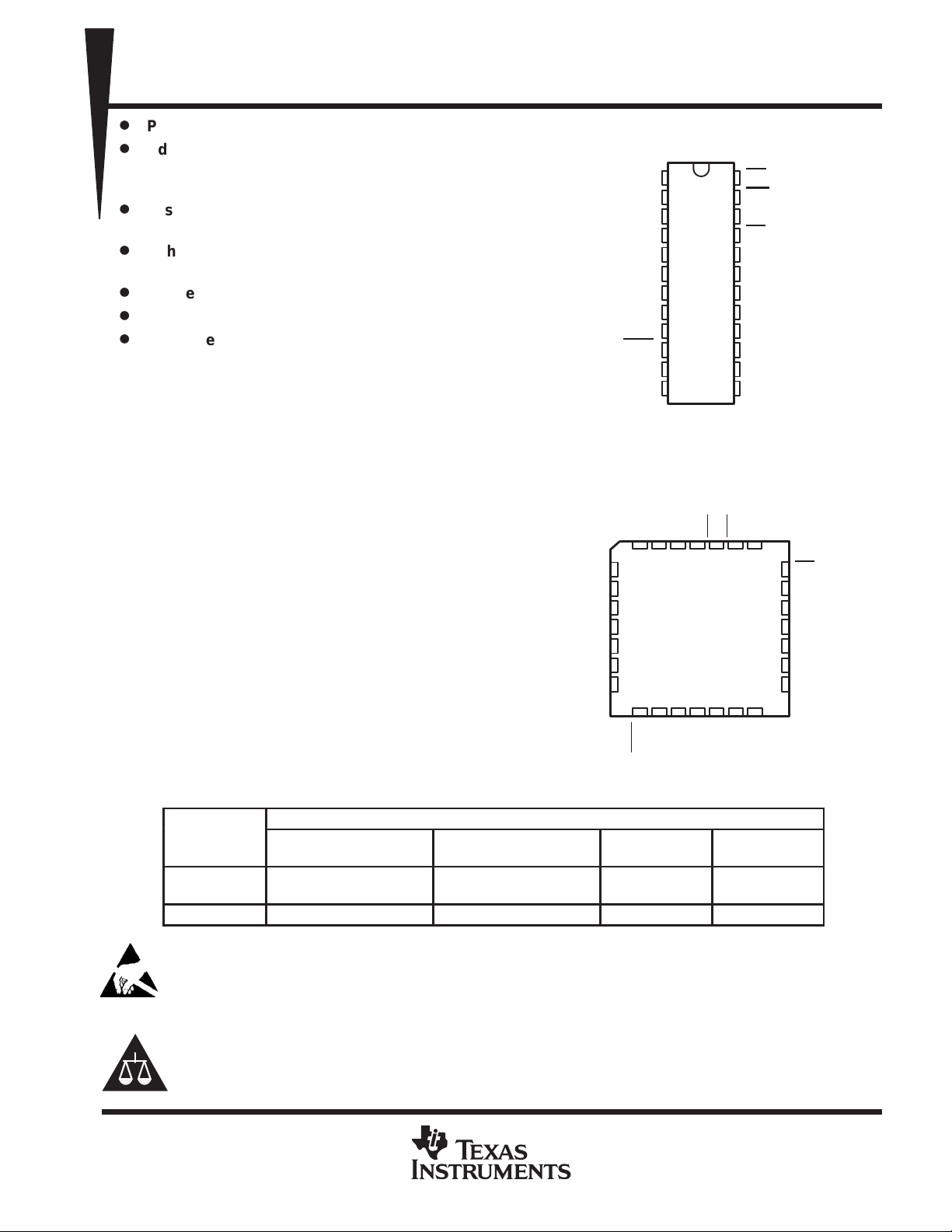
J† OR NW PACKAGE
(TOP VIEW)
REF+
REF–
ANLG GND
AIN
ANLG V
DD
DGTL GND1
DGTL GND2
DGTL V
DGTL V
DD1
DD2
EOC
D0
D1
†
Refer to the mechanical data for the JW
package.
FK OR FN PACKAGE
ANLG GND
4
321
5
AIN
ANLG V
DGTL GND1
DGTL GND2
DGTL V
DGTL V
DD
NC
DD1
DD2
6
7
8
9
10
11
12
13 14
EOC
NC – No internal connection
1
2
3
4
5
6
7
8
9
10
11
12
(TOP VIEW)
REF–
REF+
15 16 17
D0
D1NCD2D3D4
RD
24
WR
23
CLKIN
22
CS
21
D9
20
D8
19
D7
18
D6
17
D5
16
D4
15
D3
14
D2
13
RDWRCLKIN
NC
28 27 26
18
25
24
23
22
21
20
19
CS
D9
D8
NC
D7
D6
D5
AVAILABLE OPTIONS
T
A
–40°C to 85°C –
–55°C to 125°C TLC1550MFK – TLC1550MJ –
This device contains circuits to protect its inputs and outputs against damage due to high static voltages or electrostatic fields. These
circuits have been qualified to protect this device against electrostatic discharges (ESD) of up to 2 kV according to MIL-STD-883C,
Method 3015; however, it is advised that precautions be taken to avoid application of any voltage higher than maximum-rated
voltages to these high-impedance circuits. During storage or handling, the device leads should be shorted together or the device
should be placed in conductive foam. In a circuit, unused inputs should always be connected to an appropriated logic voltage level,
preferably either VCC or ground.
Please be aware that an important notice concerning availability, standard warranty, and use in critical applications of
Texas Instruments semiconductor products and disclaimers thereto appears at the end of this data sheet.
Advanced LinEPIC is a trademark of Texas Instruments Incorporated.
PRODUCTION DATA information is current as of publication date.
Products conform to specifications per the terms of Texas Instruments
standard warranty. Production processing does not necessarily include
testing of all parameters.
CERAMIC CHIP CARRIER
(FK)
POST OFFICE BOX 655303 • DALLAS, TEXAS 75265
PLASTIC CHIP CARRIER
PACKAGE
(FN)
TLC1550IFN
TLC1551IFN
CERAMIC DIP
(J)
–
Copyright 1995, Texas Instruments Incorporated
On products compliant to MIL-PRF-38535, all parameters are tested
unless otherwise noted. On all other products, production
processing does not necessarily include testing of all parameters.
PLASTIC DIP
(NW)
TLC1550INW
–
2–1
TLC1550I, TLC1550M, TLC1551I
10-BIT ANALOG-TO-DIGITAL CONVERTERS
WITH PARALLEL OUTPUTS
SLAS043C – MAY 1991 – REVISED MARCH 1995
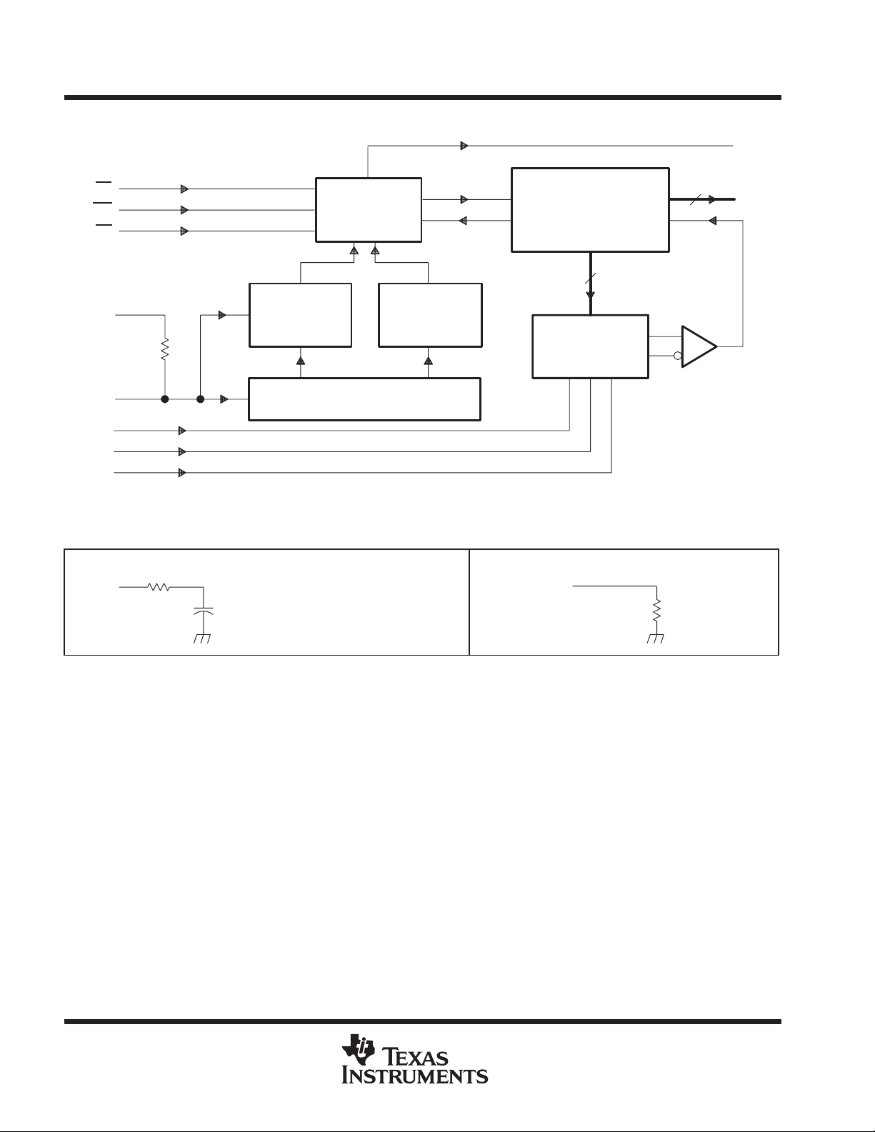
functional block diagram
EOC
CS
WR
RD
DGTL
V
DD1
100 kΩ
NOM
CLKIN
REF+
REF–
AIN
typical equivalent inputs
INPUT CIRCUIT IMPEDANCE DURING SAMPLING MODE INPUT CIRCUIT IMPEDANCE DURING HOLD MODE
1 kΩ TYP
AIN
Ci = 60 pF TYP
(equivalent input
capacitance)
Frequency
Divided by 2
Control
Logic
Clock Detector
Internal
Clock
Successive-
Approximation
Register
10
10-Bit
Capacitor
DAC and S/H
AIN
10
D0–D9
Comp
5 MΩ TYP
2–2
POST OFFICE BOX 655303 • DALLAS, TEXAS 75265
DESCRIPTION
TLC1550I, TLC1550M, TLC1551I
10-BIT ANALOG-TO-DIGITAL CONVERTERS
WITH PARALLEL OUTPUTS
SLAS043C – MAY 1991 – REVISED MARCH 1995
Terminal Functions
TERMINAL
NAME NO.†NO.
ANLG GND 4 3 Analog ground. The reference point for the voltage applied on terminals ANLG VDD, AIN, REF+, and REF–.
AIN 5 4 Analog voltage input. The voltage applied to AIN is converted to the equivalent digital output.
ANLG V
DD
CLKIN 26 22 Clock input. CLKIN is used for external clocking instead of using the internal system clock. It usually takes a
CS 25 21 Chip-select. CS must be low for RD or WR to be recognized by the A/D converter.
D0 13 11 Data bus output. D0 is bit 1 (LSB).
D1 14 12 Data bus output. D1 is bit 2.
D2 16 13 Data bus output. D2 is bit 3.
D3 17 14 Data bus output. D3 is bit 4.
D4 18 15 Data bus output. D4 is bit 5.
D5 19 16 Data bus output. D5 is bit 6.
D6 20 17 Data bus output. D6 is bit 7.
D7 21 18 Data bus output. D7 is bit 8.
D8 23 19 Data bus output. D8 is bit 9.
D9 24 20 Data bus output. D9 is bit 10 (MSB).
DGTL GND1 7 6 Digital ground 1. The ground for power supply DGTL V
DGTL GND2 9 7 Digital ground 2. The ground for power supply DGTL V
DGTL V
DD1
DGTL V
DD2
EOC 12 10 End-of-conversion. EOC goes low indicating that conversion is complete and the results have been transferred
RD 28 24 Read input. When CS is low and RD is taken low , the data is placed on the data bus from the output latch. The
REF+ 2 1 Positive voltage-reference input. Any analog input that is greater than or equal to the voltage on REF+ converts
REF– 3 2 Negative voltage reference input. Any analog input that is less than or equal to the voltage on REF– converts
WR 27 23 Write input. When CS is low , conversion is started on the rising edge of WR. On this rising edge, the ADC holds
†
Terminal numbers for FK and FN packages.
‡
Terminal numbers for J and NW packages.
6 5 Analog positive power supply voltage. The voltage applied to this terminal is designated V
10 8 Digital positive power-supply voltage 1. DGTL V
11 9 Digital positive power-supply voltage 2. DGTL V
‡
.
DD3
few microseconds before the internal clock is disabled. To use the internal clock, CLKIN should be tied high
or left unconnected.
and is the substrate connection.
DD1
.
DD2
supplies the logic. The voltage applied to DGTL V
designated V
applied to DGTL V
to the output latch. EOC
output latch stores the conversion results at the most recent negative edge of EOC
resets EOC to a high within the t
to 1111111111. Analog input voltages between REF+ and REF– convert to the appropriate result in a ratiometric
manner.
to 0000000000.
the analog input until conversion is completed. Before and after the conversion period, which is given by t
the ADC remains in the sampling mode.
DD1
.
is designated V
DD2
can be connected to the µP- or DSP-interrupt terminal or can be continuously polled.
d(EOC)
DD1
supplies only the higher-current output buffers. The voltage
DD2
.
DD2
specifications.
. The falling edge of RD
DD1
conv
is
,
POST OFFICE BOX 655303 • DALLAS, TEXAS 75265
2–3

TLC1550I, TLC1550M, TLC1551I
Operating free-air temperature, T
°C
10-BIT ANALOG-TO-DIGITAL CONVERTERS
WITH PARALLEL OUTPUTS
SLAS043C – MAY 1991 – REVISED MARCH 1995
absolute maximum ratings over operating free-air temperature range (unless otherwise noted)
Supply voltage, V
Input voltage range, V
Output voltage range, V
DD1
, V
, and V
DD2
(any input) –0.3 V to VDD + 0.3 V. . . . . . . . . . . . . . . . . . . . . . . . . . . . . . . . . . . . . . . . . . . .
I
–0.3 V to VDD + 0.3 V. . . . . . . . . . . . . . . . . . . . . . . . . . . . . . . . . . . . . . . . . . . . . . . . . . .
O
(see Note 1) 6.5 V. . . . . . . . . . . . . . . . . . . . . . . . . . . . . . . . . . . . . . . . . .
DD3
†
Peak input current (any digital input) ±10 mA. . . . . . . . . . . . . . . . . . . . . . . . . . . . . . . . . . . . . . . . . . . . . . . . . . . . . . .
Peak total input current (all inputs) ±30 mA. . . . . . . . . . . . . . . . . . . . . . . . . . . . . . . . . . . . . . . . . . . . . . . . . . . . . . . .
Operating free-air temperature range, T
: TLC1550I, TLC1551I –40°C to 85°C. . . . . . . . . . . . . . . . . . . . . . . .
A
TLC1550M –55°C to 125°C. . . . . . . . . . . . . . . . . . . . . . . . . . . . . . .
Storage temperature range, T
–65°C to 150°C. . . . . . . . . . . . . . . . . . . . . . . . . . . . . . . . . . . . . . . . . . . . . . . . . . .
stg
Case temperature for 10 seconds: FK or FN package 260°C. . . . . . . . . . . . . . . . . . . . . . . . . . . . . . . . . . . . . . . . .
Lead temperature 1,6 mm (1/16 inch) from the case for 10 seconds: J or NW package 260°C. . . . . . . . . . . .
†
Stresses beyond those listed under “absolute maximum ratings” may cause permanent damage to the device. These are stress ratings only, and
functional operation of the device at these or any other conditions beyond those indicated under “recommended operating conditions” is not
implied. Exposure to absolute-maximum-rated conditions for extended periods may affect device reliability.
NOTE 1: V
is the voltage measured at DGTL V
DD1
DGND2. V
together (and represent 0 V). When V
is the voltage measured at ANLG VDD with respect to AGND. For these specifications, all ground terminals are tied
DD3
with respect to DGND1. V
DD1
, V
DD2
, and V
DD1
is the voltage measured at DGTL V
DD2
are equal, they are referred to simply as VDD.
DD3
with respect to the
DD2
recommended operating conditions
MIN NOM MAX UNIT
Supply voltage, V
Positive reference voltage, V
Negative reference voltage, V
Differential reference voltage, V
Analog input voltage range 0 V
High-level control input voltage, V
Low-level control input voltage, V
Input clock frequency, f
Setup time, CS low before WR or RD goes low, t
Hold time, CS low after WR or RD goes high, t
WR or RD pulse duration, t
Input clock low pulse duration, t
p
NOTE 2: Analog input voltages greater than that applied to REF+ convert to all 1s (1111111111), while input voltages less than that applied to
REF– convert to all 0s (0000000000). The total unadjusted error may increase as this differential voltage falls below 4.75 V.
DD1
, V
DD2
(CLKIN)
w(WR)
p
, V
DD3
(see Note 2) V
ref+
(see Note 2) 0 V
ref–
– V
ref+
IH
IL
wL(CLKIN)
A
(see Note 2) 0.3 0.3 V
ref–
su(CS)
h(CS)
TLC155xI
TLC1550M –55 125
4.75 5 5.5 V
DD3
DD3
2 V
0.5 7.8 MHz
0 ns
0 ns
50 ns
40% of
period
–40 85
80% of
period
V
V
0.8 V
°
2–4
POST OFFICE BOX 655303 • DALLAS, TEXAS 75265

VOLLow-level output voltage
DD
,
V
IOZOff-state (high-impedance-state) output current
A
IOSShort-circuit output current
mA
CiInput capacitance
See typical equivalent inputs TLC1550/1I
pF
TLC1550I, TLC1550M, TLC1551I
10-BIT ANALOG-TO-DIGITAL CONVERTERS
WITH PARALLEL OUTPUTS
SLAS043C – MAY 1991 – REVISED MARCH 1995
electrical characteristics over recommended operating free-air temperature range,
V
DD=Vref+
V
High-level output voltage VDD = 4.75 V, IOH = –360 µA 2.4 V
OH
I
High-level input current VI = V
IH
I
Low-level input current (except CLKIN) VI = 0 –2.5 –0.005 µA
IL
I
Low-level input current (CLKIN) –150 –50 µA
IL
I
Operating supply current CS low and RD high 2 8 mA
DD
* On products compliant to MIL-STD-883, Class B, this parameter is not production tested.
†
All typical values are at VDD = 5 V, TA = 25°C.
= 4.75 to 5.5 V and V
PARAMETER TEST CONDITIONS MIN TYP†MAX UNIT
p
p
p
p
p
ref–
p
Analog inputs
Digital inputs
= 0 (unless otherwise noted)
V
= 4.75 V,
IOL = 2.4 mA
VO = VDD, CS and RD at V
VO = 0, CS and RD at V
DD
VO = 5 V, TA = 25°C 7 14
VO = 0, TA = 25°C –12 –6
p
TA = 25°C 0.4
TA = –55°C to 125°C 0.5
p
DD
DD
0.005 2.5 µA
10
–10
60 90*
5 15*
µ
p
POST OFFICE BOX 655303 • DALLAS, TEXAS 75265
2–5

TLC1550I, TLC1550M, TLC1551I
ELLinearity error
See Note 3
LSB
TLC1550M
EZSZero-scale error
See Notes 2 and 4
LSB
TLC1550M
EFSFull-scale error
See Notes 2 and 4
LSB
TLC1550M
10-BIT ANALOG-TO-DIGITAL CONVERTERS
WITH PARALLEL OUTPUTS
SLAS043C – MAY 1991 – REVISED MARCH 1995
operating characteristics over recommended operating free-air temperature range with internal
clock and minimum sampling time of 4
PARAMETER TEST CONDITIONS T
TLC1550I Full range ±0.5
TLC1551I
TLC1550I Full range ±0.5
TLC1551I
TLC1550I Full range ±0.5
TLC1551I
TLC1550I Full range ±0.5
Total unadjusted error
t
conv
t
a(D)
t
v(D)
t
dis(D)
t
d(EOC)
†
Full range is –40°C to 85°C for the TL155xI devices and –55°C to 125°C for the TLC1550M.
‡
All typical values are at VDD = 5 V, TA = 25°C.
NOTES: 2. Analog input voltages greater than that applied to REF+ convert to all 1s (1111111111), while input voltages less than that applied
Conversion time
Data access time after RD goes low 35 ns
Data valid time after RD goes high 5 ns
Disable time, delay time from RD high to high
impedance
Delay time, RD low to EOC high 0 15 ns
to REF– convert to all 0s (0000000000). The total unadjusted error may increase as this differential voltage falls below 4.75 V.
3. Linearity error is the difference between the actual analog value at the transition between any two adjacent steps and its ideal value
after zero-scale error and full-scale error have been removed.
4. Zero-scale error is the difference between the actual mid-step value and the nominal mid-step value at specified zero scale.
Full-scale error is the difference between the actual mid-step value and the nominal mid-step value at specified full scale.
5. Total unadjusted error is the difference between the actual analog value at the transition between any two adjacent steps and its
ideal value. It includes contributions from zero-scale error, full-scale error, and linearity error.
TLC1551I
TLC1550M 25°C ±1
µs, V
DD=Vref+
See Note 5
f
clock(external)
internal clock
See Figure 3
= 5 V and V
= 4.2 MHz or
= 0 (unless otherwise noted)
ref–
†
A
Full range ±1
25°C ±0.5
Full range ±1
Full range ±1
25°C ±0.5
Full range ±1
Full range ±1
25°C ±0.5
Full range ±1
Full range ±1
MIN TYP‡MAX UNIT
30 ns
LSB
6 µs
2–6
PARAMETER MEASUREMENT INFORMATION
Source Current = 6 mA
Test Point
Output
Under Test
CL = 62 pF
Vcp = voltage commutation point for switching between source and sink currents
NOTE A: Equivalent load circuit of the Teradyne A500 tester for timing parameter measurement
Figure 1. Test Load Circuit
POST OFFICE BOX 655303 • DALLAS, TEXAS 75265
See Note A
Vcp = 1 V
Sink Current = 6 mA
TLC1550I, TLC1550M, TLC1551I
10-BIT ANALOG-TO-DIGITAL CONVERTERS
WITH PARALLEL OUTPUTS
SLAS043C – MAY 1991 – REVISED MARCH 1995
APPLICATION INFORMATION
simplified analog input analysis
Using the circuit in Figure 2, the time required to charge the analog input capacitance from 0 to VS within 1/2
LSB can be derived as follows:
The capacitance charging voltage is given by
–tcń
RtC
VC+
ǒ
V
1–e
S
where
= Rs + r
R
t
i
The final voltage to 1/2 LSB is given by
i
Ǔ
(1)
(1/2 LSB) = VS – (VS/1024)
C
Equating equation 1 to equation 2 and solving for time t
–tcń
VS*
ǒ
VSń
512Ǔ+
ǒ
V
1–e
S
RtC
i
Ǔ
gives
c
and
(1/2 LSB) = Rt × Ci × ln(1024) (4)
t
c
Therefore, with the values given, the time for the analog input signal to settle is
(1/2 LSB) = (Rs + 1 kΩ) × 60 pF × ln(1024)
t
c
This time must be less than the converter sample time shown in the timing diagrams.
Driving Source
†
R
s
V
S
VI= Input voltage at AIN
VS= External driving source voltage
Rs= Source resistance
ri= Input resistance
Ci= Input capacitance
V
I
1 kΩ MAX
r
i
TLC1550/1
V
C
C
i
50 pF MAX
(2)V
(3)
(5)
†
Driving source requirements:
• Noise and distortion for the source must be equivalent to the
resolution of the converter.
• Rs must be real at the input frequency.
Figure 2. Input Circuit Including the Driving Source
POST OFFICE BOX 655303 • DALLAS, TEXAS 75265
2–7

TLC1550I, TLC1550M, TLC1551I
10-BIT ANALOG-TO-DIGITAL CONVERTERS
WITH PARALLEL OUTPUTS
SLAS043C – MAY 1991 – REVISED MARCH 1995
PRINCIPLES OF OPERATION
The operating sequence for complete data acquisition is shown in Figure 3. Processors can address the TLC1550
and TLC1551 as an external memory device by simply connecting the address lines to a decoder and the decoder
output to CS
Once CS
converted data to be presented to the data bus with a simple read command. The device remains in a sampling (track)
mode from the rising edge of EOC
After the hold mode begins, the clock controls the conversion automatically. When the conversion is complete, the
end-of-conversion (EOC
Lowering CS
. Like other peripheral devices, the write (WR) and read (RD) input signals are valid only when CS is low.
is low, the on-board system clock permits the conversion to begin with a simple write command and the
until conversion begins with the rising edge of WR, which initiates the hold mode.
) signal goes low indicating that the digital data has been transferred to the output latch.
and RD then resets EOC and transfers the data to the data bus for the processor read cycle.
CS
WR
RD
D0–D9
EOC
0.8 V
1.4 V
0.8 V
t
su(CS)
t
w(WR)
2 V
1.4 V
t
h(CS)
0.8 V
t
conv
0.8 V
0.8 V
t
a(D)
0.8 V
Figure 3. TLC1550 or TLC1551 Operating Sequence
t
su(CS)
2 V
0.8 V
t
d(EOC)
t
v(D)
Data Valid
2 V
2 V
2 V
0.8 V
0.8 V
t
h(CS)
t
dis(D)
2–8
POST OFFICE BOX 655303 • DALLAS, TEXAS 75265

IMPORTANT NOTICE
T exas Instruments and its subsidiaries (TI) reserve the right to make changes to their products or to discontinue
any product or service without notice, and advise customers to obtain the latest version of relevant information
to verify, before placing orders, that information being relied on is current and complete. All products are sold
subject to the terms and conditions of sale supplied at the time of order acknowledgement, including those
pertaining to warranty, patent infringement, and limitation of liability.
TI warrants performance of its semiconductor products to the specifications applicable at the time of sale in
accordance with TI’s standard warranty. Testing and other quality control techniques are utilized to the extent
TI deems necessary to support this warranty . Specific testing of all parameters of each device is not necessarily
performed, except those mandated by government requirements.
CERT AIN APPLICATIONS USING SEMICONDUCTOR PRODUCTS MAY INVOL VE POTENTIAL RISKS OF
DEATH, PERSONAL INJURY, OR SEVERE PROPERTY OR ENVIRONMENTAL DAMAGE (“CRITICAL
APPLICATIONS”). TI SEMICONDUCTOR PRODUCTS ARE NOT DESIGNED, AUTHORIZED, OR
WARRANTED TO BE SUITABLE FOR USE IN LIFE-SUPPORT DEVICES OR SYSTEMS OR OTHER
CRITICAL APPLICA TIONS. INCLUSION OF TI PRODUCTS IN SUCH APPLICATIONS IS UNDERST OOD TO
BE FULLY AT THE CUSTOMER’S RISK.
In order to minimize risks associated with the customer’s applications, adequate design and operating
safeguards must be provided by the customer to minimize inherent or procedural hazards.
TI assumes no liability for applications assistance or customer product design. TI does not warrant or represent
that any license, either express or implied, is granted under any patent right, copyright, mask work right, or other
intellectual property right of TI covering or relating to any combination, machine, or process in which such
semiconductor products or services might be or are used. TI’s publication of information regarding any third
party’s products or services does not constitute TI’s approval, warranty or endorsement thereof.
Copyright 1998, Texas Instruments Incorporated
 Loading...