

TL2217-285
FIXED-VOLTAGE REGULATORS
FOR SCSI ACTIVE TERMINATION
SLVS066F – NOVEMBER 1991 – REVISED JULY 1999
1
POST OFFICE BOX 655303 • DALLAS, TEXAS 75265
D
Fully Matches Parameters for SCSI
Alternative 2 Active Termination
D
Fixed 2.85-V Output
D
±1.5% Maximum Output Tolerance
at TJ = 25°C
D
1-V Maximum Dropout Voltage
D
500-mA Output Current
D
±3% Absolute Output Variation
D
Internal Overcurrent-Limiting Circuitry
D
Internal Thermal-Overload Protection
D
Internal Overvoltage Protection
description
The TL2217-285 is a low-dropout (1 V) fixedvoltage regulator specifically designed for small
computer systems interface (SCSI) alternative 2
active signal termination. The TL2217-285 1-V
maximum dropout ensures compatibility with
existing SCSI systems, while providing a wide
TERMPWR voltage range. At the same time, the
±1.5% initial tolerance on its 2.85-V output voltage
ensures a tighter line-driver current tolerance,
thereby increasing system noise margin.
The fixed 2.85-V output voltage of TL2217-285
supports the SCSI alternative 2 termination
standard, while reducing system power
consumption. The 1-V maximum dropout voltage
brings increased TERMPWR isolation, making
the device ideal for battery-powered systems. The
TL2217-285, with internal current limiting,
overvoltage protection, ESD protection, and
thermal protection, offers designers enhanced
system protection and reliability.
When configured as a SCSI active terminator, the TL2217-285 low-dropout regulator eliminates the 220-Ω and
330-Ω resistors required for each transmission line with a passive termination scheme, reducing significantly
the continuous system-power drain. When placed in series with 110-Ω resistors, the device matches the
impedance level of the transmission cable and eliminates reflections.
The TL2217-285 is characterized for operation over the virtual junction temperature range of 0°C to 125°C.
Copyright 1999, Texas Instruments Incorporated
PRODUCTION DATA information is current as of publication date.
Products conform to specifications per the terms of Texas Instruments
standard warranty. Production processing does not necessarily include
testing of all parameters.
Please be aware that an important notice concerning availability, standard warranty, and use in critical applications of
Texas Instruments semiconductor products and disclaimers thereto appears at the end of this data sheet.
1
2
3
4
5
6
7
8
9
10
20
19
18
17
16
15
14
13
12
11
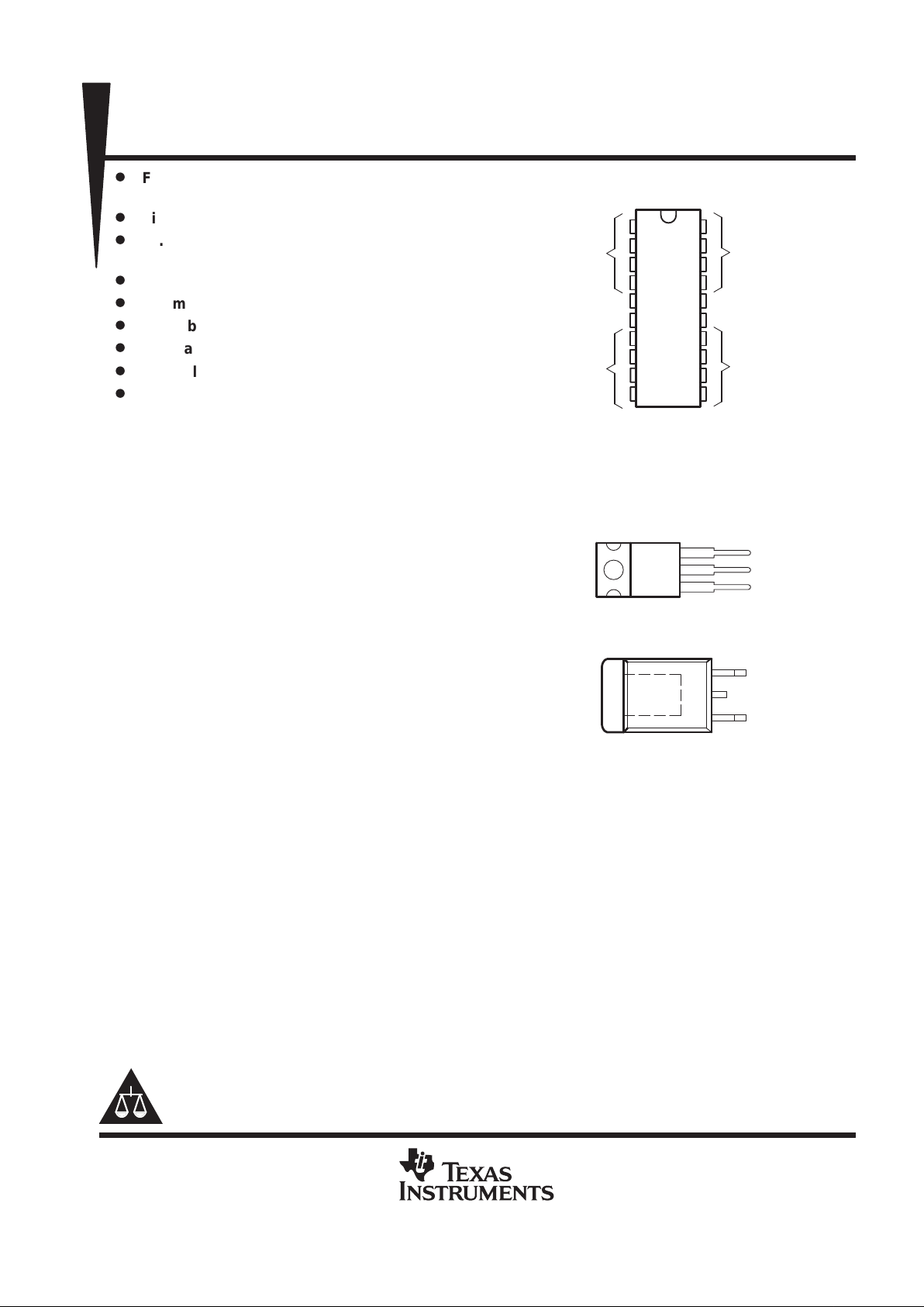
GND
OUTPUT
HEAT
SINK
HEAT
SINK
HEAT SINK – These pins have an internal
resistive connection to ground and should
be grounded or electrically isolated.
OUTPUT
GND
INPUT
GND
KTP PACKAGE
†
(TOP VIEW)
GND
†
The GND terminal is in electrical contact with
the mounting base.
GND
INPUT
HEAT
SINK
HEAT
SINK
OUTPUT
GND
INPUT
PW PACKAGE
(TOP VIEW)
KC PACKAGE
†
(TOP VIEW)
TL2217-285
FIXED-VOLTAGE REGULATORS
FOR SCSI ACTIVE TERMINATION
SLVS066F – NOVEMBER 1991 – REVISED JULY 1999
2
POST OFFICE BOX 655303 • DALLAS, TEXAS 75265
AVAILABLE OPTIONS
PACKAGED DEVICES
T
J
PLASTIC
POWER
(KC)
PLASTIC FLANGE
MOUNT
(KTP)
SURFACE
MOUNT
(PW)
CHIP
FORM
(Y)
0°C to 125°C TL2217-285KC TL22I7-285KTP TL22I7-285PWR TL2217-285Y
The KTP and PW packages are only available taped and reeled. Add the suffix R to the device type
(e.g., TL2217–285KTPR). Chip forms are tested at 25°C.
absolute maximum ratings over operating virtual junction temperature range (unless otherwise
noted)
†
Continuous input voltage, VI 7.5 V. . . . . . . . . . . . . . . . . . . . . . . . . . . . . . . . . . . . . . . . . . . . . . . . . . . . . . . . . . . . . . . .
Operating virtual junction temperature range, TJ –55°C to 150°C. . . . . . . . . . . . . . . . . . . . . . . . . . . . . . . . . . . . .
Package thermal impedance, θJA (see Notes 1 and 2): KC package 22°C/W. . . . . . . . . . . . . . . . . . . . . . . . . . .
KTP package 28°C/W. . . . . . . . . . . . . . . . . . . . . . . . . .
PW package 83°C/W. . . . . . . . . . . . . . . . . . . . . . . . . . .
Lead temperature 1,6 mm (1/16 inch) from case for 60 seconds 260°C. . . . . . . . . . . . . . . . . . . . . . . . . . . . . . .
Storage temperature range, T
stg
–65°C to 150°C. . . . . . . . . . . . . . . . . . . . . . . . . . . . . . . . . . . . . . . . . . . . . . . . . . .
†
Stresses beyond those listed under “absolute maximum ratings” may cause permanent damage to the device. These are stress ratings only, and
functional operation of the device at these or any other conditions beyond those indicated under “recommended operating conditions” is not
implied. Exposure to absolute-maximum-rated conditions for extended periods may affect device reliability.
NOTES: 1. Maximum power dissipation is a function of TJ(max),
θ
JA
, and TA. The maximum allowable power dissipation at any allowable
ambient temperature is PD = (TJ(max) – TA)/
θ
JA
. Operating at the absolute maximum TJ of 150°C can impact reliability. Due to
variations in individual device electrical characteristics and thermal resistance, the built-in thermal overload protection may be
activated at power levels slightly above or below the rated dissipation.
2. The package thermal impedance is calculated in accordance with JESD 51, except for through-hole packages, which use a trace
length of zero.
recommended operating conditions
MIN MAX UNIT
Input voltage, V
I
3.85 5.5 V
Output current, I
O
0 500 mA
Operating virtual junction temperature range, T
J
TL2217–285 0 125 °C

TL2217-285
FIXED-VOLTAGE REGULATORS
FOR SCSI ACTIVE TERMINATION
SLVS066F – NOVEMBER 1991 – REVISED JULY 1999
3
POST OFFICE BOX 655303 • DALLAS, TEXAS 75265
electrical characteristics over recommended operating conditions, V
I
= 4.5 V , IO = 500 mA, TJ = 25°C
(unless otherwise noted)
TL2217-285
PARAMETER
TEST CONDITIONS
†
MIN TYP MAX
UNIT
p
TJ = 25°C 2.81 2.85 2.89
Output voltage
I
O
= 20 mA to
500 mA
,
V
I
= 3.85 V to 5.5
V
TJ = 0°C to 125°C 2.765 2.935
V
Input voltage regulation VI = 3.85 V to 5.5 V 5 15 mV
Ripple rejection f = 120Hz, V
ripple
= 1 V
PP
–62 dB
Output voltage regulation IO = 20 mA to 500 mA 5 30 mV
Output noise voltage f = 10 Hz to 100 kHz 500 µV
Dropout voltage 1 V
IO = 0 2 5
Bias current
IO = 27 mA, equivalent 1 line asserted 3 6
mA
IO = 500 mA, equivalent 18 lines asserted (8 bit) 26 49
†
Pulse-testing techniques are used to maintain the virtual junction temperature as close to the ambient temperature as possible. Thermal effects
must be taken into account separately. All characteristics are measured with a 0.1-µF capacitor across the input and a 22-µF tantalum capacitor
with equivalent series resistance of 1.5 Ω on the output.
electrical characteristics over recommended operating conditions, V
I
= 4.5 V , I
O
= 500 mA, TJ = 25°C
(unless otherwise noted)
TL2217-285Y
PARAMETER
TEST CONDITIONS
†
MIN TYP MAX
UNIT
Output voltage IO = 20 mA to 500 mA, VI = 3.85 V to 5.5 V 2.81 2.85 2.89 V
Input voltage regulation VI = 3.85 V to 5.5 V 5 15 mV
Ripple rejection f = 120 Hz, V
ripple
= 1 V
PP
–62 dB
Output voltage regulation IO = 20 mA to 500 mA 5 30 mV
Output noise voltage f = 10 Hz to 100 kHz 500 µV
Dropout voltage IO = 500 mA 1 V
IO = 0 2 5
Bias current
IO = 27 mA, equivalent 1 line asserted 3 6
mA
IO = 500 mA, equivalent 18 lines asserted (8 bit) 26 49
†
Pulse-testing techniques are used to maintain the virtual junction temperature as close to the ambient temperature as possible. Thermal effects
must be taken into account separately. All characteristics are measured with a 0.1-µF capacitor across the input and a 22-µF tantalum capacitor
with equivalent series resistance of 1.5 Ω on the output.

TL2217-285
FIXED-VOLTAGE REGULATORS
FOR SCSI ACTIVE TERMINATION
SLVS066F – NOVEMBER 1991 – REVISED JULY 1999
4
POST OFFICE BOX 655303 • DALLAS, TEXAS 75265
COMPENSATION-CAPACITOR SELECTION INFORMATION
The TL2217-285 is a low-dropout regulator. This means that the capacitance loading is important to the performance
of the regulator because it is a vital part of the control loop. The capacitor value and the equivalent series resistance
(ESR) both affect the control loop and must be defined for the load range and the temperature range. Figure 3 and
Figure 4 can be used to establish the capacitance value and ESR range for best regulator performance.
Figure 1
2.4
2.2
2
1.8
0 0.1 0.2 0.3
ESR – Equivalent Series Resistance –
2.6
2.8
3
0.4 0.5
Not Recommended
Potential Instability
1.2
1
0.8
0.6
1.4
1.6
0.4
0.2
0
ESR (OUTPUT CAPACITOR)
vs
LOAD CURRENT
Ω
IL – Load Current – A
Applied Load
Current
Load
Voltage
∆ I
L
∆ V
L
Max ESR Boundary
Min ESR
Boundary
CL = 22 µF
CI = 0.1 µF
TJ = 25°C
Figure 2
0.02
0.015
0.005
0
0 0.5 1 1.5 2 2.5 3
0.025
0.035
3.5 4 4.5 5
0.01
0.03
0.04
STABILITY
vs
ESR
Not Recommended
Potential Instability
Recommended Min ESR
22 µF
100 µF
200 µF
400 µF
1000 µF
Region of
Best Stability
1/ESR
L
C
10 µF

TL2217-285
FIXED-VOLTAGE REGULATORS
FOR SCSI ACTIVE TERMINATION
SLVS066F – NOVEMBER 1991 – REVISED JULY 1999
5
POST OFFICE BOX 655303 • DALLAS, TEXAS 75265
APPLICATION INFORMATION
TERMPWR
Connector
1N5817
5-V
Logic
Supply
TL2217-285
OUTPUTINPUT
GND
110 Ω (each resistor)
1%
0.1 µF
+
22 µF
Tantalum
0.1 µF
Ceramic
VO = 2.85 V
DB(0)
DB(1)
ATN
BSY
RST
MSG
ACK
SEL
C/D
I/O
REQ
Figure 3. Typical Application Schematic

IMPORTANT NOTICE
T exas Instruments and its subsidiaries (TI) reserve the right to make changes to their products or to discontinue
any product or service without notice, and advise customers to obtain the latest version of relevant information
to verify, before placing orders, that information being relied on is current and complete. All products are sold
subject to the terms and conditions of sale supplied at the time of order acknowledgement, including those
pertaining to warranty, patent infringement, and limitation of liability.
TI warrants performance of its semiconductor products to the specifications applicable at the time of sale in
accordance with TI’s standard warranty. Testing and other quality control techniques are utilized to the extent
TI deems necessary to support this warranty. Specific testing of all parameters of each device is not necessarily
performed, except those mandated by government requirements.
CERT AIN APPLICATIONS USING SEMICONDUCTOR PRODUCTS MAY INVOLVE POTENTIAL RISKS OF
DEATH, PERSONAL INJURY, OR SEVERE PROPERTY OR ENVIRONMENTAL DAMAGE (“CRITICAL
APPLICATIONS”). TI SEMICONDUCTOR PRODUCTS ARE NOT DESIGNED, AUTHORIZED, OR
WARRANTED TO BE SUITABLE FOR USE IN LIFE-SUPPORT DEVICES OR SYSTEMS OR OTHER
CRITICAL APPLICATIONS. INCLUSION OF TI PRODUCTS IN SUCH APPLICA TIONS IS UNDERSTOOD T O
BE FULLY AT THE CUSTOMER’S RISK.
In order to minimize risks associated with the customer’s applications, adequate design and operating
safeguards must be provided by the customer to minimize inherent or procedural hazards.
TI assumes no liability for applications assistance or customer product design. TI does not warrant or represent
that any license, either express or implied, is granted under any patent right, copyright, mask work right, or other
intellectual property right of TI covering or relating to any combination, machine, or process in which such
semiconductor products or services might be or are used. TI’s publication of information regarding any third
party’s products or services does not constitute TI’s approval, warranty or endorsement thereof.
Copyright 1999, Texas Instruments Incorporated
 Loading...