


TL16PNP550A
ASYNCHRONOUS COMMUNICATIONS ELEMENT
WITH PLUG-AND-PLAY (PnP) AND AUTOFLOW CONTROL
SLLS190B – MARCH 1995 – REVISED MARCH 1996
1
POST OFFICE BOX 655303 • DALLAS, TEXAS 75265
D
PnP Card Autoconfiguration Sequence
Compliant
D
External Terminal-to-Bypass PnP
Autoconfiguration Sequence
D
In UART Bypass Mode, the Stand-Alone
PnP Controller is Configured With One
Logical Device
D
Provides 10-Interrupts IRQ3–IRQ7,
IRQ9–IRQ12, IRQ15
D
Simple 3-Pin Interface to SGS-Thomson
EEPROM 2K/4K ST93C56/66
D
High Output Current Drive. No External
Buffer Needed for Data and Interrupt
Signals
D
Programmable Auto-RTS and Auto-CTS
D
In Auto-CTS Mode, CTS Controls
Transmitter
D
In Auto-RTS Mode, Receiver FIFO Contents
and Threshold Control RTS
D
The Serial and Modem Control Outputs
Drive a 1-Meter RJ11 Cable Directly if
Equipment Is on the Same Power Drop
D
Capable of Running With All Existing
TL16C450 Software
D
After Reset, All Registers Are Identical to
the TL16C450 Register Set
D
Clock Prescalar Allows 22-MHz Oscillator
Clock to be Divided by 12, 6, 3, or 1
D
In the TL16C450 Mode, Hold and Shift
Registers Eliminate the Need for Precise
Synchronization Between the CPU and
Serial Data
D
Programmable Baud Rate Generator Allows
Division of Any Input Reference Clock by 1
to (2
16
–1) and Generates an Internal 16×
Clock
D
On-Chip I/O Port Address Decoding
D
In PnP Bypass Mode, 6 External Terminals
Configure the I/O Base Address and
Interrupt Mapping
D
Adds or Deletes Standard Asynchronous
Communication Bits (Start, Stop, and
Parity) to or From the Serial Data Stream
D
Independent Control of Transmit, Receive,
Line Status, and Data Set Interrupts on
Each Channel
D
Programmable Serial Interface
Characteristics:
– 5-, 6-, 7-, or 8-Bit Characters
– Even-, Odd-, or No-Parity-Bit Generation
and Detection
– 1-, 1 1/2-, or 2-Stop Bit Generation
– Baud Generation (DC to 1 Mbit Per
Second)
D
False Start Bit Detection
D
Complete Status Reporting Capabilities
D
3-State Outputs Provide TTL Drive for
Bidirectional Data Bus and Interrupt Lines
D
Line Break Generation and Detection
D
Internal Diagnostic Capabilities:
– Loopback Controls for Communications
Link Fault Isolation
– Break, Parity, Overrun, and Framing
Error Simulation
D
Fully Prioritized Interrupt System Controls
D
Modem Control Functions (CTS, RTS, DSR,
DTR, RI, and DCD)
D
Transmitter and Receiver Run at the Same
Speed
D
Up to 16-MHz Clock Rate for Up to 1-Mbaud
Operation for the Internal ACE
D
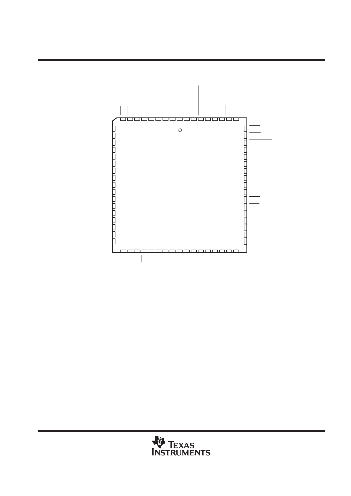
Available in 68-Pin PLCC
description
The TL16PNP550A is a functional upgrade of the TL16C550C asynchronous communications element (ACE),
which in turn is a functional upgrade of the TL16C450. Functionally equivalent to the TL16C450 on power up
(character or TL16C450 mode), the TL16PNP550A, like the TL16C550C, can be placed in an alternate mode
(FIFO mode). This relieves the CPU of excessive software overhead by buffering received and transmitted
characters. The receiver and transmitter FIFOs store up to 16 bytes including three additional bits of error status
Please be aware that an important notice concerning availability, standard warranty, and use in critical applications of
Texas Instruments semiconductor products and disclaimers thereto appears at the end of this data sheet.
PRODUCTION DATA information is current as of publication date.
Products conform to specifications per the terms of Texas Instruments
standard warranty. Production processing does not necessarily include
testing of all parameters.
Copyright 1996, Texas Instruments Incorporated
SGS-Thomson is a trademark of SGS-Thomson Incorporated.

TL16PNP550A
ASYNCHRONOUS COMMUNICATIONS ELEMENT
WITH PLUG-AND-PLAY (PnP) AND AUTOFLOW CONTROL
SLLS190B – MARCH 1995 – REVISED MARCH 1996
2
POST OFFICE BOX 655303 • DALLAS, TEXAS 75265
description (continued)
per byte for the receiver FIFO. In the FIFO mode, there is a selectable autoflow control feature that can
significantly reduce software overload and increase system efficiency by automatically controlling serial data
flow using RTS
output and CTS input signals.
The TL16PNP550A responds to the plug-and-play (PnP) autoconfiguration process. The autoconfiguration
process puts all PnP cards in a configuration mode, isolates one PnP card at a time, assigns a card select
number (CSN), and reads the card resource data structure from the EEPROM. After the resource requirements
and capabilities are determined for all cards, the autoconfiguration process uses the CSN to configure the card
by writing to the configuration registers. The TL16PNP550A only implements configuration registers for I/O
applications with one logical device and no direct memory access (DMA) support. Finally , the process activates
the TL16PNP550A card and removes it from configuration mode. After the configuration process, the ACE starts
responding to industry standard architecture (ISA) bus cycles. This device can also be configured to bypass
the PnP autoconfiguration sequence. In this mode the TL16PNP500A can be configured to select the COM port
address and IRQ level. In the UART bypass mode, the UART is disabled and this device is configured to be a
stand-alone PnP controller that supports one logical device and no DMA support.
The TL16PNP550A performs serial-to-parallel conversion on data received from a peripheral device or modem
and parallel-to-serial conversion on data received from its CPU. The CPU can read and report on the status of
the ACE operation. Reported status information includes the type of transfer operation in progress, the status
of the operation, and any error conditions encountered.
The TL16PNP550A includes a clock prescalar that divides the 22-MHz input clock by 12, 6, 3, or 1. The prescalar
output clock is fed to the programmable baud rate generator, which is capable of dividing this clock by divisors
from 1 to (2
16
– 1).
TL16PNP550A
ASYNCHRONOUS COMMUNICATIONS ELEMENT
WITH PLUG-AND-PLAY (PnP) AND AUTOFLOW CONTROL
SLLS190B – MARCH 1995 – REVISED MARCH 1996
3
POST OFFICE BOX 655303 • DALLAS, TEXAS 75265
28 29
CTS
DCD
EEPROM
SIO
V
CC
SCLK
CS
PNPS0
PNPS1
SOUT
DTR
RTS
GND
EXINTR
AEN
RESETDRV
A11
60
59
58
57
56
55
54
53
52
51
50
49
48
47
46
45
44
30
10
11
12
13
14
15
16
17
18
19
20
21
22
23
24
25
26
D0
D1
D2
D3
GND
D4
D5
D6
D7
IRQ15
IRQ3
IRQ4
V
CC
IRQ5
IRQ6
IRQ7
IRQ9
31 32 33 34
FN PACKAGE
(TOP VIEW)
ACONFIG1
ACONFIG0
87 65493
UARTBYPASS
SIN
ICONFIG3
ICONFIG2
ICONFIG1
ICONFIG0
A4A5A6
IRQ12
CS
GND
A0A1A2
A3
168672
35 36 37 38 39
66 65
27
IRQ10
IRQ11
PNPBYPASS
GND
64 63 62 61
40 41 42 43
A7A8A9
A10
XOUT
XIN
DSR
RI
IOW
IOR
V
CC
V
CC
TL16PNP550A
ASYNCHRONOUS COMMUNICATIONS ELEMENT
WITH PLUG-AND-PLAY (PnP) AND AUTOFLOW CONTROL
SLLS190B – MARCH 1995 – REVISED MARCH 1996
4
POST OFFICE BOX 655303 • DALLAS, TEXAS 75265
functional block diagram
PnP
Controller
ACE
Divide by
12, 6, 3, 1
66 67,681–4
PNPBYPASS
ACONFIG (0–1)
ICONFIG (0–4)
Oscillator
32–38, 40–44
10–13, 15–18
45
46
9
8
19–21, 23–29
55
57
54
58
SCLK
SIO
CS
EEPROM
To
EEPROM
EXINTR
UARTBYPASS
To External
Logical Device
UARTBYPASS
CS
To External
Logical Device
A0–A11
D0–D7
RESETDRV
AEN
IOW
IOR
IRQ 3–7, 9–12, 15
To ISA
Bus
SIN
SOUT
RTS
CTS
DTR
DCD
RI
6
51
49
60
50
59
61
10–13, 15–18
32–34
9
8
A0–A2
IOW
IOR
D0–D7
To RS–232
Transceivers
To ISA Bus
CLK From Prescalar
CS
_IN MR
63
64
XIN
XOUT
CLK
(to the ACE)
(prescalar)
22 MHz
INTRPT
PNPS1
PNPS0
47
7
52
53
7
30
8
3
8
8
8
2
4
DSR
62
TL16PNP550A
ASYNCHRONOUS COMMUNICATIONS ELEMENT
WITH PLUG-AND-PLAY (PnP) AND AUTOFLOW CONTROL
SLLS190B – MARCH 1995 – REVISED MARCH 1996
5
POST OFFICE BOX 655303 • DALLAS, TEXAS 75265
ACE functional block diagram
Receiver
Buffer
Register
Divisor
Latch (LS)
Divisor
Latch (MS)
Baud
Generator
Receiver
FIFO
Line
Status
Register
Transmitter
Holding
Register
Modem
Control
Register
Modem
Status
Register
Line
Control
Register
Transmitter
FIFO
Interrupt
Enable
Register
Interrupt
Identification
Register
FIFO
Control
Register
Select
and
Control
Logic
Interrupt
Control
Logic
S
e
l
e
c
t
Data
Bus
Buffer
SIN
SOUT
CTS
DTR
DSR
DCD
RI
INTRPT
60
50
62
59
61
51
6
A0
32
D(7–0)
18–15, 13 –10
Internal
Data Bus
A1
A2
CS
MR
IOR
IOW
S
e
l
e
c
t
Receiver
Shift
Register
Receiver
Timing and
Control
Transmitter
Timing and
Control
Transmitter
Shift
Register
Modem
Control
Logic
8
V
CC
V
SS
Power
Supply
RTS
49
Autoflow
Control
(AFE)
8
8
8
8
8
8
8
33
34
(from PnP)
(from PnP)
8
9
CLK
(from
Prescalar)

TL16PNP550A
ASYNCHRONOUS COMMUNICATIONS ELEMENT
WITH PLUG-AND-PLAY (PnP) AND AUTOFLOW CONTROL
SLLS190B – MARCH 1995 – REVISED MARCH 1996
6
POST OFFICE BOX 655303 • DALLAS, TEXAS 75265
Terminal Functions
TERMINAL
NAME
NO.
FN
I/O
DESCRIPTION
A0–A6
A7–A11
32–38
40–44
I 12-bit ISA address terminals. All 12 bits are used during PnP autoconfiguration sequence. After
autoconfiguration, bits A0–A2 select the ACE registers and bits A3 –A9 are used in the address decoding
to generate chip select for the device.
ACONFIG0,
ACONFIG1
67, 68 I Address configure. In PnP bypass mode, both ACONFIG0 and ACONFIG1 configure the COM port base
address.
AEN 46 I Address enable. AEN disables the ACE and PnP controller during DMA.
CS 54 O Chip select. CS is a 3-state output. It controls the activity of the EEPROM. A 100 µA pulldown circuit is
connected to this terminal.
CS 30 O Chip select. CS is the I/O chip select for the logical device.
CTS 60 I Clear to send. CTS is a modem status signal. Its condition can be checked by reading bit 4 (CTS) of the
modem status register (MSR). Bit 0 (∆CTS) of the modem status register indicates that this signal has
changed states since the last read from the MSR. When the modem status interrupt is enabled when CTS
changes states and the auto-CTS mode is not enabled, an interrupt is generated. CTS is also used in the
auto-CTS mode to control the transmitter.
D0–D3
D4–D7
10–13
15–18
I/O Data bus. D0 – D7 are eight data lines with 3-state outputs that provide a bidirectional path for data, control,
and status information between the ACE and the CPU. The output drive sinks 24 mA at 0.4 V and sources
12 mA at 2.4 V.
DCD 59 I Data carrier detect. DCD is a modem status signal. Its condition can be checked by reading bit 7 (DCD) of
the MSR. Bit 3 (∆DCD) of the MSR indicates that this signal has changed levels since the last read from the
MSR. When the modem status interrupt is enabled when DCD
changes states, an interrupt is generated.
DSR 62 I Data set ready. DSR is a modem status signal. Its condition can be checked by reading bit 5 (DSR) of the
MSR. Bit 1 (∆DSR) of the MSR indicates this signal has changed states since the last read from the MSR.
If the modem status interrupt is enabled when the DSR
changes states, an interrupt is generated.
DTR 50 O Data terminal ready . When active (low), DTR informs a modem or data set that the ACE is ready to establish
communication. DTR
is placed in its active level by setting the DTR bit of the MCR. DTR is placed in its
inactive level either as a result of a master reset, during loop mode operation, or clearing the DTR bit.
EEPROM 58 I/O EEPROM access. EEPROM is a 3-state bidirectional signal. When it is pulled low, either the TL16PNP550A
or controller is accessing the EEPROM. A 100 µA pullup circuit is connected to this terminal.
EXINTR 47 I External interrupt. During UARTBYPASS mode, the external logical device interrupt (EXINTR) is mapped
to the configured IRQs.
GND 14, 31,
48, 65
Ground (0 V). These four GND terminals must be tied to ground for proper operation.
ICONFIG0–
ICONFIG3
1–4 I IRQ configure. In PnP bypass mode, ICONFIG0, ICONFIG2, and ICONFIG3 configure the required IRQ.
IOR 8 I Read input. When IOR is active while the ACE is selected, the CPU is allowed to read from the ACE.
IOW 9 I Write input. When IOW is active while the ACE is selected, the CPU is allowed to write to the ACE.
IRQ3–IRQ4
IRQ5–IRQ7
IRQ9–IRQ12
IRQ15
20–21
23–25
26–29
19
O 3-state interrupt requests. When active (high), IRQx informs the CPU that the ACE has an interrupt to be
serviced. Four conditions that cause an interrupt to be issued are: a receiver error, received data is available
or timed out (FIFO mode only), an empty transmitter holding register, or an enabled modem status interrupt.
IRQx is generated when one or all of the above conditions occur and the value of bits 0–3 in the interrupt
request level (0×70) is equal to x (of IRQx). The output drive sinks 24 mA at 0.4 V and sources 12 mA at
2.4 V.
PNPBYPASS 66 I Bypass PnP configuration sequence. When PNPBYPASS is tied to GND, the PnP autoconfiguration
sequence is bypassed.
PNPS1–
PNPS0
52–53 O PnP internal states. See the PNPS1 and PNPS0 truth table in the PnP states section of this document.
RESETDRV 45 I Reset. When active (high), RESETDRV clears most ACE registers and puts the ACE in wait for key state.
The CSN is reset to 0×00. All configuration registers are set to their power-up values.
TL16PNP550A
ASYNCHRONOUS COMMUNICATIONS ELEMENT
WITH PLUG-AND-PLAY (PnP) AND AUTOFLOW CONTROL
SLLS190B – MARCH 1995 – REVISED MARCH 1996
7
POST OFFICE BOX 655303 • DALLAS, TEXAS 75265
Terminal Functions (Continued)
TERMINAL
NAME
NO.
FN
I/O
DESCRIPTION
RI 61 I Ring indicator. RI is modem status signal. Its condition can be checked by reading bit 6 (RI) of the MSR. BIt
2 (TERI) of the MSR indicates that RI
has transitioned from a low to a high level since the last read from the
MSR. If the modem status interrupt is enabled when this transition occurs, an interrupt is generated.
RTS 49 O Request to send. When active, RTS informs the modem or data set that the ACE is ready to receive data.
RTS
is set to its active level low by setting the RTS modem control register bit and is set to its inactive (high)
level either as a result of a master reset or during loop mode operations or by clearing bit 1 (RTS) of the MCR.
In auto-RTS mode, RTS
is set to its inactive level by the receiver threshold control logic.
SCLK 55 O 3-state EEPROM clock. SCLK is a 3-state EEPROM clock output that controls address and data transfer.
A 100 µA pulldown circuit is connected to this terminal.
SIN 6 I Serial data. SIN is input from a connected communications device.
SIO 57 I/O 3-State bidirectional EEPROM serial data bus. During output mode, SIO provides only read opcode and
address which are sourced at the falling edge of SCLK. During input mode it provides the data which is
captured at the rising edge of SCLK. A 100 µA pulldown circuit is connected to this terminal.
SOUT 51 O Composite serial data output to a connected communication device. SOUT is set to the marking (high) level
as a result of master reset.
UARTBYPASS 7 I UART bypass. When it is active, UARTBYPASS disables the UART and the TL16PNP550A acts as a PnP
stand-alone controller.
V
CC
5, 22,
39, 56
5-V supply voltage.
XIN, XOUT 63, 64 I/O External clock. XIN and XOUT connect the TL16PNP550A to the main timing reference, a 22-MHz clock or
crystal.
detailed description
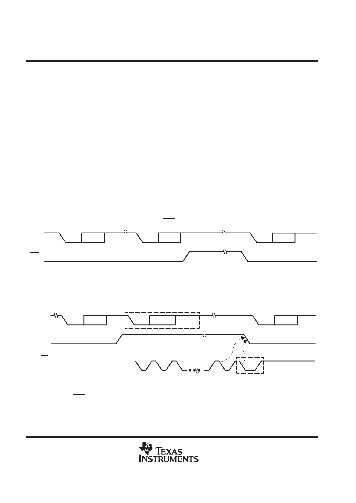
autoflow control
Autoflow control is comprised of auto-CTS and auto-RTS. With auto-CTS, the input must be active before the
transmitter FIFO can emit data (see Figure 1). Auto-RTS becomes active when the receiver needs more data
and notifies the sending serial device (see Figure 1). When RTS
is connected to CTS, data transmission does
not occur unless the receiver FIFO has space for the data; thus, overrun errors are eliminated if ACE1 and ACE2
are TL16PNP550As with enabled autoflow control. If autoflow control is not enabled, overrun errors occur when
the transmit data rate exceeds the receiver FIFO read latency.
RCV
FIFO
Serial to
Parallel
Flow
Control
XMT
FIFO
Parallel
to Serial
Flow
Control
Parallel
to Serial
Flow
Control
Serial to
Parallel
Flow
Control
XMT
FIFO
RCV
FIFO
ACE1 ACE2
D7–D0
SIN SOUT
RTS
CTS
SOUT SIN
CTS
RTS
D7–D0
Figure 1. Autoflow Control Example (Auto-RTS and Auto-CTS)
TL16PNP550A
ASYNCHRONOUS COMMUNICATIONS ELEMENT
WITH PLUG-AND-PLAY (PnP) AND AUTOFLOW CONTROL
SLLS190B – MARCH 1995 – REVISED MARCH 1996
8
POST OFFICE BOX 655303 • DALLAS, TEXAS 75265
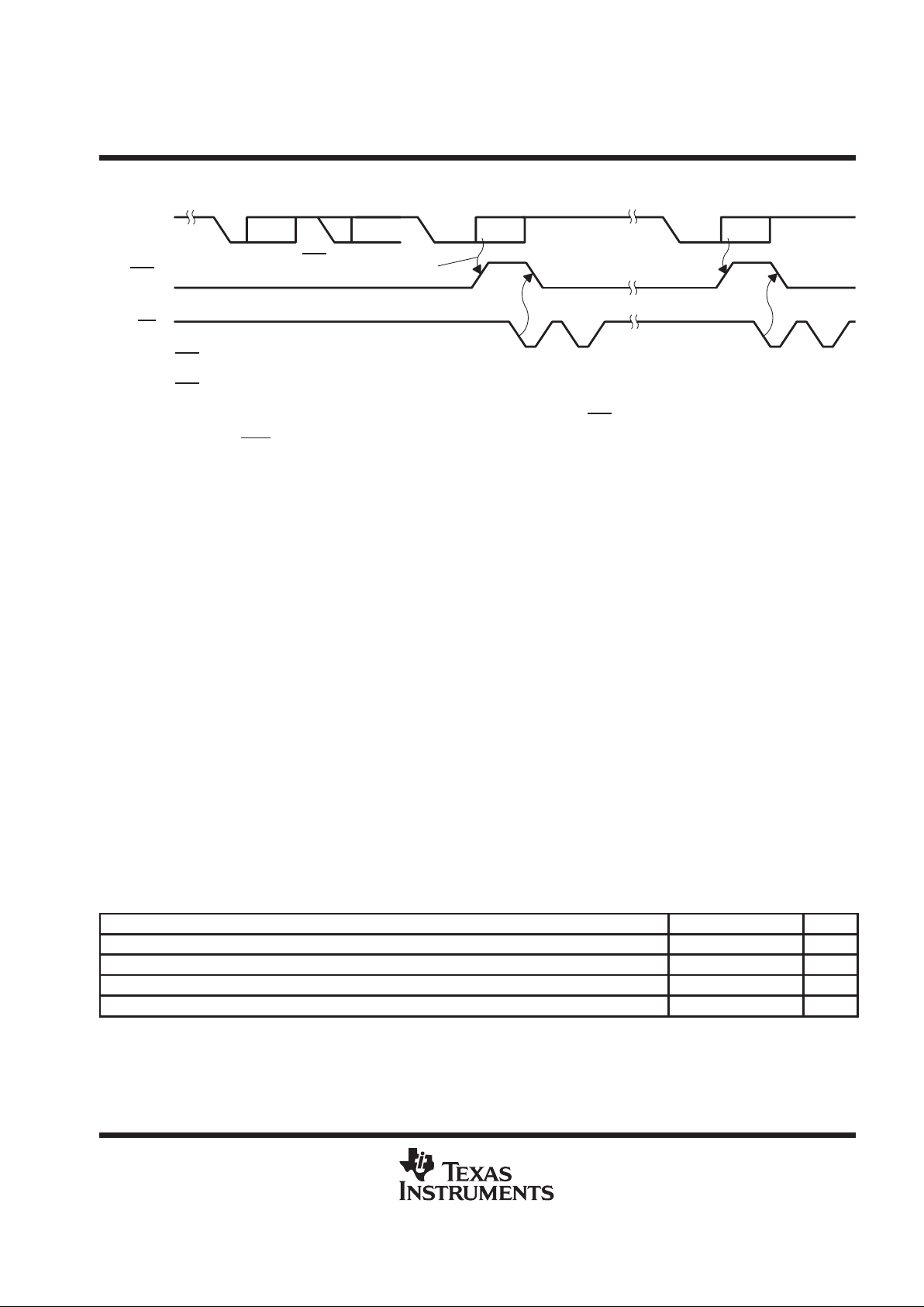
auto-RTS (see Figure 1)
Auto-RTS data flow control originates in the receiver timing and control block (see functional block diagram)
and is linked to the programmed receiver FIFO trigger level. When the receiver FIFO level reaches a trigger level
of 1, 4, or 8, (see Figure 3), RTS
is deasserted. With trigger levels of 1, 4, and 8, the sending ACE may send
an additional byte after the trigger level is reached (assuming the sending ACE has another byte to send)
because it may not recognize the deassertion of RTS
until after it has begun sending the additional byte. RTS
is automatically reasserted once the receiver FIFO is emptied by reading the receiver buffer register.
When the trigger level is 14 (see Figure 4), RTS
is deasserted after the first data bit of the sixteenth character
is present on the SIN line. RTS
is reasserted when the receiver FIFO has at least one available byte space.
auto-CTS (see Figure 1)
The transmitter circuitry checks CTS
before sending the next data byte. When CTS is active, it sends the next
byte. To stop the transmitter from sending the following byte, CTS
must be released before the middle of the
last stop bit that is currently being sent (see Figure 2). The auto-CTS function reduces interrupts to the host
system. When flow control is enabled, changes of CTS
level do not trigger host interrupts because the device
automatically controls its own transmitter. Without auto-CTS, the transmitter sends any data present in the
transmit FIFO and a receiver overrun error may result.
enabling autoflow control and auto-CTS
Autoflow control is enabled by setting modem control register bits 5 (autoflow enable or AFE) and 1 (RTS) to
1. Autoflow incorporates both auto-RTS and auto-CTS. If only auto-CTS is desired, bit 1 in the MCR should be
cleared (this assumes a control signal is driving CTS
).
Start Bits 0–7 Start Bits 0–7 Start Bits 0–7
Stop Stop Stop
SOUT
CTS
NOTE A: When CTS is low, the transmitter keeps sending serial data out. If CTS goes high before the middle of the last stop bit of the current
byte, the transmitter finishes sending the current byte but it does not send the next byte. When CTS
goes from high to low, the transmitter
begins sending data again.
Figure 2. CTS Functional Timing Waveforms
The receiver FIFO trigger level can be set to 1, 4, 8, or 14 bytes. These are described in Figures 3 and 4.
Start Byte N Start Byte N+1 Start Byte
Stop Stop Stop
SIN
RTS
RD
(RD RBR)
12
N N+1
NOTES: A. N = receiver FIFO trigger level (1, 4, or 8 bytes)
B. The two blocks in dashed lines cover the case where an additional byte is sent as described in the preceding auto-RTS section.
Figure 3. RTS Functional Timing Waveforms, Receiver FIFO Trigger Level = 1, 4, or 8 Bytes
TL16PNP550A
ASYNCHRONOUS COMMUNICATIONS ELEMENT
WITH PLUG-AND-PLAY (PnP) AND AUTOFLOW CONTROL
SLLS190B – MARCH 1995 – REVISED MARCH 1996
9
POST OFFICE BOX 655303 • DALLAS, TEXAS 75265
enabling autoflow control and auto-CTS (continued)
Byte 14 Byte 15
SIN
RTS
RD
(RD RBR)
Start Byte 18 StopStart Byte 16 Stop
RTS Released After the
First Data Bit of Byte 16
NOTES: A. RTS is deasserted when the receiver receives the first data bit of the sixteenth byte. The receiver FIFO is full after finishing the
sixteenth byte.
B. RTS
is asserted again when there is at least one byte of space available and no incoming byte is in processing or there is more than
one byte of space available.
C. When the receiver FIFO is full, the first receiver buffer register read reasserts RTS
.
Figure 4. RTS Functional Timing Waveforms, Receiver FIFO Trigger Level = 14 Bytes
flow control and interrupt
When flow control is enabled, bit 0 (∆CTS) of the modem status register does not cause a modem status
interrupt. The ACE accommodates a 1-Mbaud serial rate (16-MHz input clock) so that a bit time is 1 µs, and
a typical character time is 10 µs (start bit, 8 data bits, and a stop bit).
The TL16PNP550A ACE includes a programmable, on-board, baud rate generator that divides a reference
clock input by 1 to (2
16
– 1) for producing a 16 × clock to drive the internal transmitter logic. Provisions are
included to use this 16 × clock to drive the receiver logic. The ACE includes complete modem control capability
and a processor interrupt system that may be software tailored to minimize the system overhead for handling
the communications link.
absolute maximum ratings over operating free-air temperature range (unless otherwise noted)
†
Supply voltage range, V
CC
(see Note 1) –0.5 V to 7 V. . . . . . . . . . . . . . . . . . . . . . . . . . . . . . . . . . . . . . . . . . . . . .
Input voltage range at any input, V
I
–0.5 V to 7 V. . . . . . . . . . . . . . . . . . . . . . . . . . . . . . . . . . . . . . . . . . . . . . . . . . .
Output voltage range, V
O
–0.5 V to 7 V. . . . . . . . . . . . . . . . . . . . . . . . . . . . . . . . . . . . . . . . . . . . . . . . . . . . . . . . . . .
Operating free-air temperature range, T
A
0°C to 70°C. . . . . . . . . . . . . . . . . . . . . . . . . . . . . . . . . . . . . . . . . . . . . .
Storage temperature range, T
stg
–65°C to 150°C. . . . . . . . . . . . . . . . . . . . . . . . . . . . . . . . . . . . . . . . . . . . . . . . . .
Case temperature for 10 seconds, T
C
: FN package 260°C. . . . . . . . . . . . . . . . . . . . . . . . . . . . . . . . . . . . . . . . . .
†
Stresses beyond those listed under “absolute maximum ratings” may cause permanent damage to the device. These are stress ratings only, and
functional operation of the device at these or any other conditions beyond those indicated under “recommended operating conditions” is not
implied. Exposure to absolute-maximum-rated conditions for extended periods may affect device reliability.
NOTE 1: All voltage values are with respect to VSS.
recommended operating conditions
MIN NOM MAX UNIT
Supply voltage, V
CC
4.75 5 5.25 V
High-level input voltage, V
IH
2 V
CC
V
Low-level input voltage, V
IL
–0.5 0.8 V
Operating free-air temperature, T
A
0 70 °C
TL16PNP550A
ASYNCHRONOUS COMMUNICATIONS ELEMENT
WITH PLUG-AND-PLAY (PnP) AND AUTOFLOW CONTROL
SLLS190B – MARCH 1995 – REVISED MARCH 1996
10
POST OFFICE BOX 655303 • DALLAS, TEXAS 75265
electrical characteristics over recommended ranges of supply voltage and operating free-air
temperature (unless otherwise noted)
PARAMETER TEST CONDITIONS MIN TYP†MAX UNIT
V
OH
‡
High-level output voltage IOH = –12 mA VCC–0.8 V
V
OL
‡
Low-level output voltage IOL = 24 mA 0.5 V
V
OH
High-level output voltage
IOH = –4 mA (see Note 2),
VCC = 0.8 V
VCC–0.8 V
V
OL
Low-level output voltage IOL = 4 mA (see Note 2) 0.5 V
p
V
= 5.25 V , V
= 0,
IlInput current
CC
,
VI = 0 to 5.25 V,
SS
,
All other terminals floating
±1µA
V
= 5.25 V,V
= 0
,
I
OZ
High-i
mpedance-state output cur-
V
CC
5.25 V, V
SS
0,
VO = 0 to 5.25 V,
±10 µA
OZ
rent
O
Pullup and pulldown circuits are off
µ
VCC = 5.25 V , TA = 25°C,
CC A
SIN, DSR, DCD, CTS, and RI at 2 V ,
I
CC
Supply current
All other inputs at 0.8 V ,
5mA
CC
y
Clock at 4 MHz (no crystal used)
,
No load on outputs
,
No load on out uts,
Baud rate = 50 kbit/s
C
i(CLK)
Clock input capacitance 15 20 pF
C
o(CLK)
Clock output capacitance
VCC = 0, VSS = 0,
20 30 pF
C
i
Input capacitance
f
= 1 MHz,
T
A
=
25°C
,
All oth
e
r terminals groun
ded
6 10 pF
C
o
Output capacitance
All other terminals grounded
10 20 pF
f
(XIN–XOUT)
Oscillator speed (XIN and XOUT) 16 22 MHz
†
All typical values are at VCC = 5 V and TA = 25°C.
‡
These parameters apply only for IRQx and D7–D0.
NOTE 2: These parameters apply for all outputs except XOUT, IRQx, and D7–D0.
clock timing requirements over recommended ranges of supply voltage and operating free-air
temperature
PARAMETER
ALTERNATE
SYMBOLS
TEST
CONDITIONS
MIN MAX UNIT
t
d1
Delay time, chip select (CS) high to clock (SCLK) high t
SHCH
50 ns
t
d2
Input valid to clock (SCLK) high t
DVCH
100 ns
t
pd1
Propagation delay time, clock (SCLK) high to input transition
(SIO)
t
CHDX
100 ns
t
pd2
Propagation delay time, clock (SCLK) high to output valid
(SIO)
t
CHQV
500 ns
t
pd3
Propagation delay time, clock (SCLK) low to chip select
transition (CS)
t
CLSL
See Figure 18
and Figure 19
2
clock
periods
t
d3
Delay time, chip select (CS) low to output Hi-Z (SIO) t
SLQZ
100 ns
t
w(SCLKH)
Pulse duration, clock (SCLK) high to clock (SCLK) low
(see Note 3)
t
CHCL
250 ns
t
w(SCLKL)
Pulse duration, clock (SCLK) low to clock (SCLK) high
(see Note 3)
t
CLCH
250 ns
f
clock
Clock frequency (SCLK) (see Note 4) F
CLK
0.5 0.68 MHz
NOTES: 3. The ST93C56 chip select, S, must be brought low for a minimum of 250 ns (t
SLSH
) between consecutive instruction cycles according
to the ST93C56 specification.
4. The SCLK signal is attained by internally frequency dividing the XIN signal by 32.
TL16PNP550A
ASYNCHRONOUS COMMUNICATIONS ELEMENT
WITH PLUG-AND-PLAY (PnP) AND AUTOFLOW CONTROL
SLLS190B – MARCH 1995 – REVISED MARCH 1996
11
POST OFFICE BOX 655303 • DALLAS, TEXAS 75265
system timing requirements over recommended ranges of supply voltage and operating free-air
temperature
PARAMETER
ALTERNATE
SYMBOL
FIGURE TEST CONDITIONS MIN MAX UNIT
t
cR
Cycle time, read (tw7 + td8 + td9) RC 87 ns
t
cW
Cycle time, write (tw6 + td5 + td6) WC 87 ns
t
w1
†
Pulse duration, XIN high t
XH
Figure 5 f = 16 MHz maximum 25 ns
t
w2
†
Pulse duration, XIN low t
XL
Figure 5 f = 16 MHz maximum 25 ns
t
w6
Pulse duration, write strobe (IOW) t
WR
Figure 6 75 ns
t
w7
Pulse duration, read strobe (IOR) t
RD
Figure 7 75 ns
t
w8
Pulse duration, master reset t
MR
1 µs
t
su3
Setup time, data valid before
IOW
↑ t
DS
Figure 6 15 ns
t
h1
Hold time, chip select (CS) valid after address (A0
– A2) becomes invalid
t
CH
Figure 6,
Figure 7
From the first rising
edge of XIN after
address invalid
20 ns
t
h2
Hold time, data valid after IOW↑ t
DH
Figure 6 5 ns
t
d4
Delay time, chip select (CS) valid after address
valid (A0 – A2)
t
CSRW
Figure 6,
Figure 7
From the first rising
edge of XIN after
address valid
30 ns
t
d5
Delay time, address valid (A0 – A2) before
IOW
↓ t
AW
Figure 6 7 ns
t
d6
Delay time, address valid (A0 – A2) before
IOR
↓ t
AR
Figure 7 7 ns
t
d7
Delay time, chip select (CS) valid to data valid
(D7 – D0)
t
CSVD
Figure 7 CL = 75 pF 30 ns
t
d8
Delay time,
IOR
↑ to floating data (D7 – D0) t
HZ
Figure 7 CL = 75 pF 20 ns
t
d9
Delay time, EXINTR↑
or EXINTR
↓ to IRQx↑
or
IRQx
↓
Figure 8 15 ns
†
This only applies when PNPBYPASS is low.
oscillator cell maximum switching characteristics, VCC = 4.75 V, TJ = 115°C
FROM TO
INTRINSIC
DELTA
DELAY (ns)
PARAMETER
(INPUT) (OUTPUT)
DELAY
(ns)
DELAY
(ns/pF)
CL = 15 pF CL = 50 pF CL = 85 pF CL = 100 pF
t
PLH
–0.25 0.300 4.26 14.76 25.26 29.77
t
PHL
XIN
XOUT
–0.24 0.206 2.85 10.06 17.27 20.36
t
r
Output rise time, XOUT 5.83 21.15 36.47 43.04
t
f
Output fall time, XOUT 3.76 13.50 23.24 27.41
baud generator switching characteristics over recommended ranges of supply voltage and
operating free-air temperature, C
L
= 75 pF (see Figure 5)
PARAMETER
ALTERNATE
SYMBOL
TEST CONDITIONS MIN MAX UNIT
t
w3
†
Pulse duration, PNPS1 low t
LW
f = 16 MHz, CLK ÷ 2 50 ns
t
w4
†
Pulse duration, PNPS1 high t
HW
f = 16 MHz, CLK ÷ 2 50 ns
t
d1
†
Delay time, XIN↑ to PNPS1↑ t
BLD
45 ns
t
d2
†
Delay time, XIN↑↓ to PNPS1↓ t
BHD
45 ns
†
This only applies when PNPBYPASS
is low.
TL16PNP550A
ASYNCHRONOUS COMMUNICATIONS ELEMENT
WITH PLUG-AND-PLAY (PnP) AND AUTOFLOW CONTROL
SLLS190B – MARCH 1995 – REVISED MARCH 1996
12
POST OFFICE BOX 655303 • DALLAS, TEXAS 75265
receiver switching characteristics over recommended ranges of supply voltage and operating
free-air temperature (see Note 5)
PARAMETER
ALTERNATE
SYMBOL
FIGURE TEST CONDITIONS MIN MAX UNIT
t
d10
Delay time, stop (SIN) to set INTRPT or read
RBR to LSI interrupt (IRQx)
t
SINT
Figure 9,
Figure 10,
Figure 11
1
RCLK
cycle
t
d11
Delay time, read RBR/LSR (IOR) to reset
INTRPT (IRQx)
t
RINT
Figure 9,
Figure 10,
Figure 11
CL = 75 pF 70 ns
NOTE 5: In the FIFO mode, the read cycle (RC) = 425 ns (min) between reads of the receiver FIFO and the status registers (interrupt identification
register or line status register).
transmitter switching characteristics over recommended ranges of supply voltage and operating
free-air temperature (see Figure 12)
PARAMETER
ALTERNATE
SYMBOL
TEST CONDITIONS MIN MAX UNIT
t
d12
Delay time, initial write (IRQx) to transmit start (SOUT) t
IRS
8 26
baudout
cycles
t
d13
Delay time, start (SOUT) to INTRPT (IRQx) t
STI
8 10
baudout
cycles
t
d14
Delay time, IOW (WR THR) to reset INTRPT (IRQx) t
HR
CL = 75 pF 50 ns
t
d15
Delay time, initial write (IOW) to INTRPT (THRE†) (IRQx) t
SI
16 34
baudout
cycles
t
d16
Delay time, read IIR† (IOR) to reset INTRPT (THRE†)
(IRQx)
t
IR
CL = 75 pF 35 ns
†
THRE = transmitter holding register empty; IIR = interrupt identification register.
modem control switching characteristics over recommended ranges of supply voltage and
operating free-air temperature, C
L
= 75 pF
PARAMETER
ALTERNATE
SYMBOL
FIGURE MIN MAX UNIT
t
d17
Delay time, WR MCR (IOW) to output (RTS, DTS) t
MDO
Figure 13 50 ns
t
d18
Delay time, modem interrupt (CTS, DSR, DCD/RI) to set INTRPT
(IRQx)
t
SIM
Figure 13 35 ns
t
d19
Delay time, RD MSR (IOR) to reset INTRPT (IRQx) t
RIM
Figure 13 40 ns
t
d20
Delay time, CTS low to SOUT↓ Figure 14 24
baudout
cycles
t
d21
Delay time, receiver threshold byte (SIN) to RTS↑ Figure 15 3
baudout
cycles
t
d22
Delay time, read of last byte in receiver FIFO (IOR) to RTS↓ Figure 15 3
baudout
cycles
t
d23
Delay time, first data bit of 16th character (SIN) to RTS↑ Figure 16 3
baudout
cycles
t
d24
Delay time, RD RBR (IOR) ↓ to RTS↓ Figure 16 3
baudout
cycles

TL16PNP550A
ASYNCHRONOUS COMMUNICATIONS ELEMENT
WITH PLUG-AND-PLAY (PnP) AND AUTOFLOW CONTROL
SLLS190B – MARCH 1995 – REVISED MARCH 1996
13
POST OFFICE BOX 655303 • DALLAS, TEXAS 75265
PARAMETER MEASUREMENT INFORMATION
PNPS1
(1/1)
XIN
PNPS1
(1/2)
PNPS1
(1/3)
PNPS1
(1/N)
(N > 3)
2 XIN Cycles
(N–2) XIN Cycles
t
w3
t
w4
t
d1
t
d2
t
d1
t
d2
N
t
w1
t
w2
NOTE A: When PNPBYPASS
= 0, the PNPS1 terminal is acting as the BAUDOUT . The above timing assumes
that the prescalar value is one.
Figure 5. Baud Generator Timing Waveforms
t
su3
t
h2
t
d4
t
h1
Valid Data
Valid Address
Valid
A0–A2
CS
D7–D0
50% 50%
50% 50%
Active50% 50%
t
w6
t
d5
XIN
IOW
NOTE A: The above timing assumes that AEN = 0.
Figure 6. Write Cycle Timing Waveforms

TL16PNP550A
ASYNCHRONOUS COMMUNICATIONS ELEMENT
WITH PLUG-AND-PLAY (PnP) AND AUTOFLOW CONTROL
SLLS190B – MARCH 1995 – REVISED MARCH 1996
14
POST OFFICE BOX 655303 • DALLAS, TEXAS 75265
PARAMETER MEASUREMENT INFORMATION
t
d7
t
d8
t
d4
t
h1
Valid Data
Valid Address
Valid
A0–A2
CS
D7–D0
50% 50%
50% 50%
Active50% 50%
t
d6
XIN
IOR
t
w7
Figure 7. Read Cycle Timing Waveforms
t
d9
EXINTR
IRQx
UARTBYPASS
t
d9
Figure 8. External Interrupt (EXINTR) Timing Waveforms

TL16PNP550A
ASYNCHRONOUS COMMUNICATIONS ELEMENT
WITH PLUG-AND-PLAY (PnP) AND AUTOFLOW CONTROL
SLLS190B – MARCH 1995 – REVISED MARCH 1996
15
POST OFFICE BOX 655303 • DALLAS, TEXAS 75265
PARAMETER MEASUREMENT INFORMATION
t
d10
Active
Active
IOR
(RD RBR)
RCLK
(see Note A)
t
d11
8 CLKs
Parity StopStart Data Bits 5–8
Sample Clock
TL16C450 Mode:
Sample Clock
SIN
IRQx
(data ready)
(see Note B)
IRQx
(RCV error)
(see Note B)
IOR
(RD LSR)
50%50%
50%
50%
50%
50%
t
d11
NOTES: A. RCLK is the internal receiver clock.
B. X = 3–5, 7–12, 15
Figure 9. Receiver Timing Waveforms

TL16PNP550A
ASYNCHRONOUS COMMUNICATIONS ELEMENT
WITH PLUG-AND-PLAY (PnP) AND AUTOFLOW CONTROL
SLLS190B – MARCH 1995 – REVISED MARCH 1996
16
POST OFFICE BOX 655303 • DALLAS, TEXAS 75265
PARAMETER MEASUREMENT INFORMATION
t
d10
(see Note A)
t
d11
Stop
Data Bits 5–8
Sample Clock
SIN
Trigger Level
IRQx
(FCR6, 7 = 0, 0)
IRQx
Line Status
Interrupt (LSI)
t
d11
IOR
(RD LSR)
IOR
(RD RBR)
Active
Active
(FIFO at or above
trigger level)
(FIFO below
trigger level)
50%50%
50%
50%
50%
50%
NOTE A: For a time-out interrupt, t
d10
= 9 RCLKs.
Figure 10. Receive FIFO First Byte (Sets DR Bit) Waveforms
t
d10
(see Note A)
t
d11
Stop
Top Byte of FIFO
Sample Clock
SIN
Time-Out or IRQx
Trigger Level
Interrupt
IRQx
Line Status
Interrupt (LSI)
t
d10
(FIFO at or above
trigger level)
(FIFO below
trigger level)
IOR
(RD LSR)
IOR
(RD RBR)
Active Active
t
d11
Previous Byte
Read From FIFO
50%
50%
50%50%
50%
50% 50%
NOTE A: For a time-out interrupt, t
d10
= 9 RCLKs.
Figure 11. Receive FIFO Bytes Other Than the First Byte (DR Internal Bit Already Set) Waveforms

TL16PNP550A
ASYNCHRONOUS COMMUNICATIONS ELEMENT
WITH PLUG-AND-PLAY (PnP) AND AUTOFLOW CONTROL
SLLS190B – MARCH 1995 – REVISED MARCH 1996
17
POST OFFICE BOX 655303 • DALLAS, TEXAS 75265
PARAMETER MEASUREMENT INFORMATION
t
d13
Parity Stop
Start
Data Bits
SOUT
Start
t
d12
t
d14
t
d14
t
d15
t
d16
IRQx
(THRE)
IOW
(WR THR)
IOR
(RD IIR)
50% 50% 50% 50% 50%
50%
50%
50%
50%
50%
50%
Figure 12. Transmitter Timing Waveforms
t
d17
t
d17
IOW
(WR MCR)
RTS, DTR
CTS, DSR, DCD
t
d18
t
d19
t
d18
IRQx
(modem)
IOR
(RD MSR)
RI
50% 50%
50% 50%
50%
50%
50%
50%
50%
50%
Figure 13. Modem Control Timing Waveforms

TL16PNP550A
ASYNCHRONOUS COMMUNICATIONS ELEMENT
WITH PLUG-AND-PLAY (PnP) AND AUTOFLOW CONTROL
SLLS190B – MARCH 1995 – REVISED MARCH 1996
18
POST OFFICE BOX 655303 • DALLAS, TEXAS 75265
PARAMETER MEASUREMENT INFORMATION
Midpoint of Stop Bit
t
d20
t
su4
CTS
SOUT
50% 50%
50%
Figure 14. CTS and SOUT Autoflow Control Timing (Start and Stop) Waveforms
t
d22
SIN
50%
t
d21
50%
50%
Midpoint of Stop Bit
RTS
IOR
(RD RBR)
Figure 15. Auto-RTS Timing for Receiver Threshold of 1, 4, or 8 Waveforms
t
d24
SIN
50%
t
d23
50%
50%
Midpoint of Data Bit 0
RTS
15th Character 16th Character
IOR
RD RBR)
Figure 16. Auto-RTS Timing for Receiver Threshold of 14 Waveforms

TL16PNP550A
ASYNCHRONOUS COMMUNICATIONS ELEMENT
WITH PLUG-AND-PLAY (PnP) AND AUTOFLOW CONTROL
SLLS190B – MARCH 1995 – REVISED MARCH 1996
19
POST OFFICE BOX 655303 • DALLAS, TEXAS 75265
PRINCIPLES OF OPERATION
The TL16PNP550A architecture (see functional block diagram) has been designed, so that it can be configured
in various operational modes. These modes are described in the Table 1.
Table 1. TL16PNP550A Operational Modes
†
MODE DESCRIPTION
UARTBYPASS
TERMINAL
PNPBYPASS
TERMINAL
ICONFIG<3:0>
TERMINAL
ACONFIG <1:0>
TERMINAL
PnP controller and logical device (ACE) 0 1 X X
Stand-alone PnP Controller 1 1 X X
ACE TL16C550C only 0 0 Active Active
Manufacturer test mode
‡
1 0 X X
†
X = irrelevant, 0 = low level, 1 = high level
‡
During manufacturer test mode, the oscillator clock is disabled. This mode is used by the manufacturer for test only.
Connecting the PNPBYPASS terminal to VCC enables the PnP autoconfiguration sequence. When PnP is
enabled, the ACONFIG<1:0> and ICONFIG<3:0> are irrelevant and should be tied to GND or V
CC
.
In the stand-alone PnP controller mode, the controller responds to the autoconfiguration sequence and supports
one logical device, one I/O address, one interrupt, and no DMA. The address decoder only decodes eight
contiguous locations. During this mode, the UART is disabled and CS
and EXINTR terminals become active.
The UART input terminals should be tied to either V
CC
or GND to avoid floating input terminals.
When PnP is disabled or bypassed, the PNPBYP ASS
terminal is tied to GND and the configuration in Table 2
applies.
Table 2. PnP Disabled or Bypassed Configuration
ACONFIG<1:0> COM I/O BASE ADDRESS
00 COM1 3F8–3FF
01 COM2 2F8–2FF
10 COM3 3E8–3EF
11 COM4 2E8–2EF
The decimal value X of ICONFIG<3:0> content enables the corresponding IRQx. For example,
ICONFIG<3:0> = 0011 enables IRQ3 (Table 3).
Table 3. ICONFIG to IRQx
ICONFIG IRQx ICONFIG IRQx
0000 N/A 1000 N/A
0001 N/A 1001 IRQ9
0010 N/A 1010 IRQ10
0011 IRQ3 1011 IRQ11
0100 IRQ4 1100 IRQ12
0101 IRQ5 1101 N/A
0110 IRQ6 1110 N/A
0111 IRQ7 1111 IRQ15

TL16PNP550A
ASYNCHRONOUS COMMUNICATIONS ELEMENT
WITH PLUG-AND-PLAY (PnP) AND AUTOFLOW CONTROL
SLLS190B – MARCH 1995 – REVISED MARCH 1996
20
POST OFFICE BOX 655303 • DALLAS, TEXAS 75265
PRINCIPLES OF OPERATION
PnP card configuration sequence
The PnP logic is quiescent on power up and must be enabled by software. The following sequence configures
the PnP card:
1. The initiation key places the PnP logic into configuration mode through a series of predefined writes to
the ADDRESS port (see autoconfiguration ports section).
2. A serial identifier is accessed bit serially and isolates the Industry Standard Architecture (ISA) cards.
Seventy-two READ_DATA port reads are required to isolate each card.
3. Once isolated, a card is assigned a handle [card select number (CSN)] that later selects the card. This
assignment is accomplished by programming the CSN.
4. The PnP software then reads the resource data structure on each card. When all resource capabilities
and demands are known, a process of resource arbitration is invoked to determine resource allocation
for each card.
5. All PnP cards are then activated and removed from the configuration mode. This activation is
accomplished by programming the ACTIVE register.
PnP autoconfiguration ports
Three 8-bit ports (see Table 4) are used by the software to access the configuration space on each PnP ISA
card. These registers are used by the PnP software to issue commands, check status, access the resource data
information, and configure the PnP hardware.
The ports have been chosen so as to avoid conflicts in the installed base of ISA functions, while at the same
time minimizing the number of ports needed in the ISA I/O space.
Table 4. Autoconfiguration Ports
PORT NAME LOCATION TYPE
ADDRESS 0×0279 (printer status port) Write only
WRITE_DATA 0×0A79 (printer status port + 0×0800) Write only
READ_DATA Relocatable in range 0×0203 to 0×03FF Read only
The PnP registers are accessed by first writing the address of the desired register to the ADDRESS port,
followed by a read of data from the READ_DATA port, or a write of data to the WRITE_DATA port. Once
addressed, the desired register may be accessed using the WRITE_DATA or READ_DATA ports.
The ADDRESS port is also the destination of the initiation key writes.
The address of the READ_DA TA port is set by programming the SET RD_DA T A PORT register . If a card cannot
be isolated for a given READ_DAT A port address, the READ_DA TA port address is in conflict. The READ_DA T A
port address must then be relocated and the isolation process begun again. The entire range between 0×0203
and 0 ×3FF is available; however, in practice it is expected that only a few address locations are necessary
before the software determines that no PnP cards are present

TL16PNP550A
ASYNCHRONOUS COMMUNICATIONS ELEMENT
WITH PLUG-AND-PLAY (PnP) AND AUTOFLOW CONTROL
SLLS190B – MARCH 1995 – REVISED MARCH 1996
21
POST OFFICE BOX 655303 • DALLAS, TEXAS 75265
PRINCIPLES OF OPERATION
PnP registers
PnP card standard registers are divided into three parts: card control, logical device control, and logical device
configuration. There is exactly one of each card control register on each ISA card. Card control registers are
used for global functions that control the entire card (see Table 5). Logical device control registers and logical
device configuration registers are repeated for each logical device. Since the TL16PNP550A has one logical
device (ACE) and it is intended only for I/O applications, not all the configuration registers are implemented.
Table 5. PnP Card Control Registers
ADDRESS PORT
VALUE
REGISTER NAME VALUE
READ/WRITE
CAPABILITY
POWER UP
0×00 SET RD_DATA PORT Write only 00 00 00 00
Writing to this location modifies the address port used for reading from the PnP ISA card. Writing to this register is
only allowed when the card is in the isolation state.
Bit<7:0> Become I/O port address bits [9:2].
0×01 SERIAL ISOLATION Read only 00 00 00 00
A read to this register causes a card in the isolation state to compare one bit of the board ID.
0×02 CONFIGURATION CONTROL Write only 0 00
This 3-bit register consists of three independent commands, which are activated by setting their corresponding
register bits. These bits are automatically cleared by the hardware after the commands execute.
Bit<2> Setting this bit causes the card to clear its CSN and RD DATA port.
Bit<1> Setting this bit causes the card to enter the wait for key state, but the card CSN is
preserved and the logical device (ACE) is unaffected.
Bit<0> Setting this bit resets the logical device (ACE) configuration registers to their default
state and the CSN is preserved.
0×03 WAKE[CSN] Write only 00 00 00 00
A write to this register, if the write data [7:0] matches the card CSN, causes the card to go from the sleep state to
either the isolation state, if the write data for this command is zero, or the configuration state if the write data is not
zero. The pointer to the SERIAL IDENTIFIER is reset. This register is write only.
0×04 RESOURCE DATA Read only 00 00 00 00
A read from this address reads the next byte of resource information from the EPROM. The STA TUS register must
be polled until its bit<0> is set, before this register may be read.
0×05 STATUS Read only 0
Bit<0> A 1-bit register that when set, indicates it is okay to read the next data byte from the RESOURCE
DATA register .
0×06 CARD SELECT NUMBER Read/write 00 00 00 00
A write to this address sets a card CSN, which is uniquely assigned to this card after the serial identification process,
so each card may be individually selected during a WAKE [CSN] command.
0×07 LOGICAL DEVICE NUMBER Read 00 00 00 00
This register has a read-only value of 0×00, since the card has only 1 logical device.

TL16PNP550A
ASYNCHRONOUS COMMUNICATIONS ELEMENT
WITH PLUG-AND-PLAY (PnP) AND AUTOFLOW CONTROL
SLLS190B – MARCH 1995 – REVISED MARCH 1996
22
POST OFFICE BOX 655303 • DALLAS, TEXAS 75265
PRINCIPLES OF OPERATION
PnP logical device control registers
The following registers are repeated for each logical device. These registers control device functions, such as
enabling the device onto the ISA bus (see Table 6).
Table 6. PnP Logical Device Control Registers
ADDRESS PORT
VALUE
REGISTER NAME VALUE
READ/WRITE
CAPABILITY
POWER UP
0×30 ACTIVE Read/write 00 00 00 00
This register controls whether the logical device is active on the bus.
Bit<7:1> Reserved and must be cleared.
Bit<0> When set, activates the logical device.
An inactive device does not respond to nor drive any ISA bus signals. Before a logical device is activated, I/O range
check must be disabled.
0×31 I/O RANGE CHECK Read/write 00 00 00 00
This register performs a conflict check on the I/O port range programmed for use by the logical device.
Bit<7:2> Reserved and must be cleared.
Bit<1> When set, I/O range check is enabled. I/O range check is only valid, when the logical device is
inactive.
Bit<0> When set, the logical device (an ACE in this case) responds to I/O reads of the logical device
(ACE) assigned I/O range with a 0×55 when I/O range check is in operation. When clear, the
logical device responds with a 0×AA. This register is read/write.
PnP logical device configuration registers
These registers program the device ISA bus resource use (see Table 7).
Table 7. PnP Logical Device Configuration Registers
ADDRESS PORT
VALUE
REGISTER NAME VALUE
READ/WRITE
CAPABILITY
POWER UP
0×60 I/O PORT BASE ADDRESS [15:8] Read/write 00
This register indicates the selected I/O upper limit address bits [15:8] for I/O descriptor 0. When the device is
activated, if there is an address match to register 0 ×61 and an address match to this register, a chip select is
generated.
Bit<7:2> Bits 15–10 are not supported, since the logical device uses 10-bit address decoding.
Bit<1:0> Indicates address bits 9 and 8.
0×61 I/O PORT BASE ADDRESS [7:0] Read/write 00 00 00 00
This register indicates the selected I/O lower limit address bits [7:0] for I/O descriptor 0. When the device is activated,
if there is an address match to register 0×60 and an address match to this register, a chip select is generated.
Bit<2:0> Are not supported since the logical device has eight registers.
Bit<7:3> Indicates address bits 7–3.
0×70 INTERRUPT REQUEST LEVEL SELECT Read/write 00 00
This register indicates the selected interrupt level.
Bit<3:0> Select the interrupt level. This device uses 10 interrupts from IRQ2 to IRQ7 and IRQ9 to IRQ12.
0×71 INTERRUPT REQUEST TYPE Read 00 00 00 11
This register indicates which type of interrupt is used for the selected interrupt level.
Bit<7:2> Are reserved.
Bit<1> Is set to indicate active high.
Bit<0> Is set to indicate level sensitive.
0×74 DMA CHANNEL SELECT 0 Read only 00 00 01 00
This register has a value of 4 to indicate that DMA is not supported.
0×75 DMA CHANNEL SELECT 1 Read only 00 00 01 00
This register has a value of 4 to indicate that DMA is not supported.

TL16PNP550A
ASYNCHRONOUS COMMUNICATIONS ELEMENT
WITH PLUG-AND-PLAY (PnP) AND AUTOFLOW CONTROL
SLLS190B – MARCH 1995 – REVISED MARCH 1996
23
POST OFFICE BOX 655303 • DALLAS, TEXAS 75265
PRINCIPLES OF OPERATION
PnP terminal states
Terminals PNPS1 and PNPS0 reflect the states of PnP logic when PNPBYPASS is set (see Table 8).
Table 8. PNPx Terminal States
PNPS1 PNPS0 PnP STATE
0
0
1
1
0
1
0
1
WAIT FOR KEY
SLEEP
ISOLATION
CONFIGURATION
If the device leaves the wait-for-key state, it means the device is in configuration mode.
Please note, when PNPBYPASS
= 0, BAUDOUT is monitored using PNPS1 and RXRDY is monitored using
PNPS0.
EEPROM
The TL16PNP550A has been designed to interface with the ST93C56/66 EEPROM (SGS-Thomson) or
equivalent. The EEPROM provides the clock prescalar divisor and PnP resource data.
memory organization
The EEPROM should be organized as 128/255 words times 16 bits, so its ORG terminal should be connected
to V
CC
or left unconnected. The EEPROM memory organization is shown in Table 9.
T able 9. EEPROM Memory Organization
EEPROM
LOCATION
15 14 13 12 11 10 9 8 7 6 5 4 3 2 1 0
BIT LOCATION
X 0 0 0
X 128/255
PnP Resource Data

TL16PNP550A
ASYNCHRONOUS COMMUNICATIONS ELEMENT
WITH PLUG-AND-PLAY (PnP) AND AUTOFLOW CONTROL
SLLS190B – MARCH 1995 – REVISED MARCH 1996
24
POST OFFICE BOX 655303 • DALLAS, TEXAS 75265
PRINCIPLES OF OPERATION
clock prescalar
The TL16PNP550A includes a clock prescalar block. The block takes the 22-MHz input clock and divides it by
a divisor read from the EEPROM at address zero. After reset, the device reads the EEPROM content at address
zero. The 2 most significant data bits of the word (2 bytes) define the divisor value as show in Table 10.
Table 10. Default Deviser Value
EEPROM LOCATION
000 (BITS 15 AND 14)
DIVISOR VALUE
00 12
01 6
10 3
11 1 (default)
The device monitors the EEPROM to check whether the divisor value has been updated or not. Read the
EEPROM interface section for more details in this mode. Note the EEPROM address location zero is reserved
for the divisor value.
EEPROM signal description (see Figure 17)
13 5
246
1. During and after reset, the TL16PNP550A gains access to EEPROM interface by asserting EEPROM (low).
The device reads the prescalar divisor value from address zero. After it receives the WAKE command, the
device starts receiving PnP resource data from address location 00x01H.
2. After the device is configured and leaves the configuration mode (the device is activated and it is in the wait
for key state), the TL16PNP550A releases the EEPROM interface by releasing signals EEPROM
, SCLK,
SIO, and CS.
3. The on-board controller is accessing the EEPROM.
4. The TL16PNP550A assumes the prescalar divisor value has been updated.
5. The TL16PNP550A accesses the EEPROM by asserting EEPROM
signal. It reads location 00 and updates
the prescalar divisor.
6. The TL16PNP550A releases the EEPROM
signal and SCLK, CS and SIO signals.
If the device enters the configuration mode again (leaves the wait for key state), it gains access directly to the
EEPROM after the EEPROM
signal is released.
If the EEPROM
is driven by an on-board controller and the TL16PNP550A enters the configuration mode, it is
highly recommended that the controller release the EEPROM
signal to allow the TL16PNP550A to gain control
of EEPROM
. It is possible to deactivate and reconfigure the TL16PNP550A when it enters the configuration
mode. PNPS0 and PNPS1 terminals inform the controller when the TL16PNP550A enters the configuration
mode.

TL16PNP550A
ASYNCHRONOUS COMMUNICATIONS ELEMENT
WITH PLUG-AND-PLAY (PnP) AND AUTOFLOW CONTROL
SLLS190B – MARCH 1995 – REVISED MARCH 1996
25
POST OFFICE BOX 655303 • DALLAS, TEXAS 75265
PRINCIPLES OF OPERATION
EEPROM
EEPROM
Interface
Control
(optional)
EEPROM
CPU
ISA Bus
SIO
CS
SCLK
D
Q
S
C
TL16PNP550A
NOTE A: It is recommended that a 2-kΩ resistor be connected between D and Q terminals.
Figure 17. TL16PNP550A and EEPROM Interface
EEPROM READ
The TL16PNP550A only supports read transactions. The READ op code instruction (10) must be sent into the
EEPROM. The op code is then followed by an address for the 16-bit word, which is 8-bits long . The READ op
code with accompanying address directs the EEPROM to output serial data on the EEPROM data terminal D/Q
which is connected to the TL16PNP550A bidirectional serial data bus (SIO). Specifically , when a READ op code
and address are received, the instruction and address are decoded and the addressed EEPROM data is
transferred into an output shift register in the EEPROM. Each read transaction consists of a start bit, 2-bit op
code (10), 8-bit address, and 16-bit data. The TL16PNP550A does not accommodate the EEPROM
auto-address next word feature.

TL16PNP550A
ASYNCHRONOUS COMMUNICATIONS ELEMENT
WITH PLUG-AND-PLAY (PnP) AND AUTOFLOW CONTROL
SLLS190B – MARCH 1995 – REVISED MARCH 1996
26
POST OFFICE BOX 655303 • DALLAS, TEXAS 75265
PRINCIPLES OF OPERATION
READ op code transfer (see Figure 18)
Initially , the EEPROM chip select signal, S, which is connected to the TL16PNP550A EEPROM chip select (CS),
is raised. The EEPROM data, D/Q then samples the TL16PNP550A (SIO) line on the following rising edges of
the TL16PNP550A clock (SCLK), until a 1 is sampled and decoded by the EEPROM as a start bit. The
TL16PNP550A (SCLK) signal is connected to the EEPROM clock, C. The READ op code (10) is then sampled
on the next two rising edges of SCLK. TL16PNP550A sources the op code at the falling edges of SCLK.
t
d1
Start Op Code Input
Op Code Input = 1Start Op Code Input = 0
t
d2
t
w(SCLKH)
t
w(SCLKL)
t
pd1
C
(SCLK)
S
(CS)
D/Q
(SIO)
NOTE A: The corresponding TL16PNP550A terminal names are provided in parentheses. D/Q indicates that D and Q terminals in the EEPROMs
are tied together with a 2-kΩ resistor.
Figure 18. READ Op Code Transfer Waveforms
READ address and data transfer (see Figure 19)
After receiving the READ op code, the EEPROM samples the READ address on the next eight rising edges of
(SCLK). The device sources the address at the falling edge of SCLK. The EEPROM then sends out a dummy
0 bit on the D/Q line, which is followed by the 16-bit data word with the MSB first. Output data changes are
triggered by the rising edges of SCLK. The data is also read by the TL16PNP550A on the rising edges of SCLK.
t
d2
t
pd1
t
pd2
t
d3
t
pd3
Address Input Data Output
C
(SCLK)
S
(CS)
D/Q
(SIO)
NOTE A: The corresponding terminal names are provided in parentheses. D/Q indicates that D and Q terminals in the EEPROMs are tied together
with a 2-kΩ resistor.
Figure 19. READ Address and Data Transfer Waveforms

TL16PNP550A
ASYNCHRONOUS COMMUNICATIONS ELEMENT
WITH PLUG-AND-PLAY (PnP) AND AUTOFLOW CONTROL
SLLS190B – MARCH 1995 – REVISED MARCH 1996
27
POST OFFICE BOX 655303 • DALLAS, TEXAS 75265
PRINCIPLES OF OPERATION
Table 11. ACE Register Selection
DLAB
†
A2 A1 A0 REGISTER
0 L L L Receiver buffer (read), transmitter holding register (write)
0 L L H Interrupt enable
X L H L Interrupt identification (read only)
X L H L FIFO control (write)
X L H H Line control
X H L L Modem control
X H L H Line status
X H H L Modem status
X H H H Scratch
1 L L L Divisor latch (LSB)
1 L L H Divisor latch (MSB)
†
The divisor latch access bit (DLAB) is the most significant bit of the line control register . The DLAB signal
is controlled by writing to this bit location (see Table 13).
Table 12. ACE Reset Functions
REGISTER/SIGNAL
RESET
CONTROL
RESET STATE
Interrupt Enable Register Master Reset All bits cleared (0–3 forced and 4–7 permanent)
Interrupt Identification Register Master Reset
Bit 0 is set, bits 1–3, 6, 7 are cleared, and bits 4–5 are
permanently cleared
FIFO Control Register Master Reset All bits cleared
Line Control Register Master Reset All bits cleared
Modem Control Register Master Reset All bits cleared (6–7 permanent)
Line Status Register Master Reset Bits 5 and 6 are set, all other bits are cleared
Modem Status Register Master Reset Bits 0–3 are cleared, bits 4–7 are input signals
SOUT Master Reset High
INTRPT (receiver error flag) Read LSR/MR Low
INTRPT (received data available) Read RBR/MR Low
INTRPT (transmitter holding register empty) Read IR/Write THR/MR Low
INTRPT (modem status changes) Read MSR/MR Low
RTS Master Reset High
DTR Master Reset High
Scratch Register Master Reset No effect
Divisor Latch (LSB and MSB) Registers Master Reset No effect
Receiver Buffer Registers Master Reset No effect
Transmitter Holding Register Master Reset No effect
Receiver FIFO
MR/FCR1–FCR0/
∆FCR0
All bits cleared
XMIT FIFO
MR/FCR2–FCR0/
∆FCR0
All bits cleared

TL16PNP550A
ASYNCHRONOUS COMMUNICATIONS ELEMENT
WITH PLUG-AND-PLAY (PnP) AND AUTOFLOW CONTROL
SLLS190B – MARCH 1995 – REVISED MARCH 1996
28
POST OFFICE BOX 655303 • DALLAS, TEXAS 75265
PRINCIPLES OF OPERATION
accessible registers
The system programmer, using the CPU, has access to and control over any of the ACE registers. These
registers control ACE operations, receive data, and transmit data. Descriptions of these registers follow in
Table 13.
T able 13. Summary of Accessible Registers
REGISTER ADDRESS
0DLAB=0 0DLAB=0 1 DLAB = 0 2 2 3 4 5 6 7 0 DLAB = 1 1 DLAB =1
Bit
No.
Receiver
Buffer
Register
(Read
Only)
Transmitter
Holding
Register
(Write
Only)
Interrupt
Enable
Register
Interrupt
Ident.
Register
(Read
Only)
FIFO
Control
Register
(Write
Only)
Line
Control
Register
Modem
Control
Register
Line
Status
Register
Modem
Status
Register
Scratch
Register
Divisor
Latch
(LSB)
Latch
(MSB)
RBR THR IER IIR FCR LCR MCR LSR MSR SCR DLL DLM
0 Data Bit 0†Data Bit 0
Enable
Received
Data
Available
Interrupt
(ERBI)
0 If
Interrupt
Pending
FIFO
Enable
Word
Length
Select
Bit 0
(WLS0)
Data
Terminal
Ready
(DTR)
Data
Ready
(DR)
Delta
Clear
to Send
(
∆CTS)
Bit 0 Bit 0 Bit 8
1 Data Bit 1 Data Bit 1
Enable
Transmitter
Holding
Register
Empty
Interrupt
(ETBEI)
Interrupt
ID
Bit 1
Receiver
FIFO
Reset
Word
Length
Select
Bit 1
(WLS1)
Request
to Send
(RTS)
Overrun
Error
(OE)
Delta
Data
Set
Ready
(
∆DSR)
Bit 1 Bit 1 Bit 9
2 Data Bit 2 Data Bit 2
Enable
Receiver
Line Status
Interrupt
(ELSI)
Interrupt
ID
Bit 2
Transmitter
FIFO
Reset
Number
of
Stop Bits
(STB)
OUT1
Parity
Error
(PE)
Trailing
Edge of
Ring
Indicator
(TERI)
Bit 2 Bit 2 Bit 10
3 Data Bit 3 Data Bit 3
Enable
Modem
Status
Interrupt
(EDSSI)
Interrupt
ID
Bit 3
‡
Reserved
Parity
Enable
(PEN)
OUT2
UART
Interrupt
Enable
§
Framing
Error
(FE)
Delta
Data
Carrier
Detect
(
∆DCD)
Bit 3 Bit 3 Bit 11
4 Data Bit 4 Data Bit 4 0 0 Reserved
Even
Parity
Select
(EPS)
Loop
Break
Interrupt
(BI)
Clear
to
Send
(CTS)
Bit 4 Bit 4 Bit 12
5 Data Bit 5 Data Bit 5 0 0 Reserved
Stick
Parity
Flow
Control
Enable
(AUTO)
Transmitter
Holding
Register
(THRE)
Data
Set
Ready
(DSR)
Bit 5 Bit 5 Bit 13
6 Data Bit 6 Data Bit 6 0
FIFOs
Enabled
‡
Receiver
Trigger
(LSB)
Break
Control
0
Transmitter
Empty
(TEMT)
Ring
Indicator
(RI)
Bit 6 Bit 6 Bit 14
7 Data Bit 7 Data Bit 7 0
FIFOs
Enabled
‡
Receiver
Trigger
(MSB)
Divisor
Latch
Access
Bit
(DLAB)
0
Error in
Receiver
FIFO
(see
Note 6)
Data
Carrier
Detect
(DCD)
Bit 7 Bit 7 Bit 15
†
Bit 0 is the least significant bit. It is the first bit serially transmitted or received.
‡
These bits are always 0 in the TL16C450 mode.
§
By setting this bit high in PNPBYPASS mode, the selected interrupt (IRQx) is enabled, otherwise, IRQx output is in the high-impedance state.
TL16PNP550A
ASYNCHRONOUS COMMUNICATIONS ELEMENT
WITH PLUG-AND-PLAY (PnP) AND AUTOFLOW CONTROL
SLLS190B – MARCH 1995 – REVISED MARCH 1996
29
POST OFFICE BOX 655303 • DALLAS, TEXAS 75265
PRINCIPLES OF OPERATION
FIFO control register (FCR)
The FCR is a write-only register at the same location as the IIR, which is a read-only register. The FCR enables
the FIFOs, clears the FIFOs, sets the receiver FIFO trigger level, and selects the type of DMA signaling.
D
Bit 0: FCR0, when set, enables the transmit and receive FIFOs. This bit must be set when other FCR bits
are written to or they are not programmed. Changing this bit clears the FIFOs.
D
Bit 1: FCR1, when set, clears all bytes in the receiver FIFO and resets its counter . The shift register is not
cleared. The logic 1 that is written to this bit position is self clearing.
D
Bit 2: FCR2, when set, clears all bytes in the transmit FIFO and resets its counter . The shift register is not
cleared. The logic 1 that is written to this bit position is self clearing.
D
Bits 3, 4, and 5: FCR3, FCR4, and FCR5 are reserved for future use.
D
Bits 6 and 7: FCR6 and FCR7 set the trigger level for the receiver FIFO interrupt (see Table 14).
Table 14. Receiver FIFO Trigger Level
BIT 7 BIT 6
RECEIVER FIFO
TRIGGER LEVEL (BYTES)
0 0 01
0 1 04
1 0 08
1 1 14
FIFO interrupt mode operation
When the receiver FIFO and receiver interrupts are enabled (FCR0 = 1, IER0 = 1, IER2 = 1), receiver interrupt
occur as follows:
1. When the receiver FIFO reaches its programmed trigger level, the received data available interrupt is
issued to the microprocessor and IIR (3–0) are set to the value 6 (to indicate received data available).
The received data available interrupt is cleared and IIR (3–0) are set (no interrupt) when the FIFO drops
below its programmed trigger level.
2. The data ready bit (LSR0) is set as soon as a character is transferred from the shift register to the
receiver FIFO. It is cleared when the FIFO is empty.
3. The receiver line status interrupt (IIR = 0110h) has higher priority than the received data available
(IIR = 0100h) interrupt.

TL16PNP550A
ASYNCHRONOUS COMMUNICATIONS ELEMENT
WITH PLUG-AND-PLAY (PnP) AND AUTOFLOW CONTROL
SLLS190B – MARCH 1995 – REVISED MARCH 1996
30
POST OFFICE BOX 655303 • DALLAS, TEXAS 75265
PRINCIPLES OF OPERATION
FIFO interrupt mode operation (continued)
When the receiver FIFO and receiver interrupts are enabled, receiver FIFO time-out interrupt occurs as follows:
1. FIFO time-out interrupt occurs when the following conditions exist:
a. At least one character is in the FIFO.
b. The most recent serial character received is longer than the four previous continuous character
times (if two stop bits are programmed, the second one is included in this time delay).
c. The most recent microprocessor read of the FIFO is longer than four previous continuous character
times. This causes a maximum character received to interrupt an issued delay of 160 ms at
300 baud with a 12-bit character.
2. Character times are calculated by using the internal receiver clock (RCLK) input for a clock signal (makes
the delay proportional to the baud rate). The RCLK frequency equals the clock frequency generated by the
prescalar block divided by the user-defined internal UART baud rate generator divisor.
3. When a time-out interrupt has occurred, it is cleared and the timer is reset when the microprocessor reads
one character from the receiver FIFO.
4. When a time-out interrupt has not occurred, the time-out timer is reset after a new character is received or
after the microprocessor reads the receiver FIFO.
When the transmit FIFO and transmitter interrupts are enabled (FCR0 = 1, IER1 = 1), transmit interrupts occur
as follows:
1. The transmitter holding register empty interrupt [IIR (3–0) = 2] occurs when the transmit FIFO is empty. It
is cleared [IIR (3–0) = 1] as soon as the THR is written to (1 to 16 characters may be written to the transmit
FIFO while servicing this interrupt) or the IIR is read.
2. The transmitter FIFO empty indicator [LSR5 (THRE) = 1] is delayed one character time minus the last stop
bit time when there have not been at least two bytes in the transmitter FIFO at the same time since the last
time that THRE = 1. The first transmitter interrupt after changing FCR0 is immediate when it is enabled.
Character time-out and receiver FIFO trigger level interrupts have the same priority as the current received data
available interrupt; transmit FIFO empty has the same priority as the current transmitter holding register empty
interrupt.
FIFO polled mode operation
With FCR0 = 1 (transmitter and receiver FIFOs enabled), clearing IER0, IER1, IER2, IER3, or all four puts the
ACE in the FIFO polled mode of operation. Since the receiver and transmitter are controlled separately , either
one or both can be in the polled mode of operation.
In this mode, the user program checks receiver and transmitter status using the LSR.
• LSR0 is set as long as there is one byte in the receiver FIFO.
• LSR1 – LSR4 specify which error(s) have occurred. Character error status is handled the same way as
when in the interrupt mode; the IIR is not affected since IER2 = 0.
• LSR5 indicates when the transmit FIFO is empty.
• LSR6 indicates that both the transmit FIFO and shift registers are empty.
• LSR7 indicates whether there are any errors in the receiver FIFO.
There is no trigger level reached or time-out condition indicated in the FIFO polled mode. However, the receiver
and transmit FIFOs are still fully capable of holding characters.

TL16PNP550A
ASYNCHRONOUS COMMUNICATIONS ELEMENT
WITH PLUG-AND-PLAY (PnP) AND AUTOFLOW CONTROL
SLLS190B – MARCH 1995 – REVISED MARCH 1996
31
POST OFFICE BOX 655303 • DALLAS, TEXAS 75265
PRINCIPLES OF OPERATION
interrupt enable register (IER)
The IER enables each of the five types of interrupts (refer to Table 15) and the internal INTRPT output signal
in response to an interrupt generation. The IER can also disable the interrupt system by clearing bits 0 through
3. The contents of this register are summarized in Table 13 and are described in the following bulleted list.
D
Bit 0: This bit, when set, enables the received data available interrupt.
D
Bit 1: This bit, when set, enables the transmitter holding register empty interrupt.
D
Bit 2: This bit, when set, enables the receiver line status interrupt.
D
Bit 3: This bit, when set, enables the modem status interrupt.
D
Bits 4 – 7: These bits in the IER are not used and are always cleared.
interrupt identification register (IIR)
The ACE has an on-chip interrupt generation and prioritization capability that permits a flexible interface with
most popular microprocessors.
The ACE provides four prioritized levels of interrupts:
D
Priority 1– Receiver line status (highest priority)
D
Priority 2– Receiver data ready or receiver character time out
D
Priority 3–Transmitter holding register empty
D
Priority 4–Modem status (lowest priority)
When an interrupt is generated, the IIR indicates that an interrupt is pending and the type of that interrupt in its
three least significant bits (bits 0, 1, and 2). The contents of this register are summarized in Table 13 and
described in Table 15. Details on each bit are as follows:
D
Bit 0: This bit can be used either in a hardwire prioritized, or polled interrupt system. When this bit is cleared,
an interrupt is pending. When bit 0 is set, no interrupt is pending.
D
Bits 1 and 2: These two bits identify the highest priority interrupt pending, as indicated in Table 15.
D
Bit 3: This bit is always cleared in the TL16C450 mode. In FIFO mode, this bit is set with bit 2 to indicate
that a time-out interrupt is pending.
D
Bits 4 and 5: These two bits are not used and are always cleared.
D
Bits 6 and 7: These two bits are always cleared in the TL16C450 mode. They are set when bit 0 of the FIFO
control register is set.

TL16PNP550A
ASYNCHRONOUS COMMUNICATIONS ELEMENT
WITH PLUG-AND-PLAY (PnP) AND AUTOFLOW CONTROL
SLLS190B – MARCH 1995 – REVISED MARCH 1996
32
POST OFFICE BOX 655303 • DALLAS, TEXAS 75265
PRINCIPLES OF OPERATION
interrupt identification register (IIR) (continued)
Table 15. Interrupt Control Functions
INTERRUPT
IDENTIFICATION
REGISTER
PRIORITY
LEVEL
INTERRUPT TYPE INTERRUPT SOURCE
INTERRUPT RESET
METHOD
BIT 3 BIT 2 BIT 1 BIT 0
0 0 0 1 None None None None
0 1 1 0 1 Receiver line status
Overrun error, parity error,
framing error or break interrupt
Reading the line status register
0 1 0 0 2 Received data available
Receiver data available in the
TL16C450 mode or trigger level
reached in the FIFO mode
Reading the receiver buffer
register
1 1 0 0 2
Character time-out
indication
No characters have been
removed from or input to the
receiver FIFO during the last
four character times, and there
is at least one character in it
during this time
Reading the receiver buffer
register
0 0 1 0 3
Transmitter holding
register empty
Transmitter holding register
empty
Reading the interrupt
identification register (if source
of interrupt) or writing into the
transmitter holding register
0 0 0 0 4 Modem status
Clear to send, data set ready,
ring indicator, or data carrier
detect
Reading the modem status
register
line control register (LCR)
The system programmer controls the format of the asynchronous data communication exchange through the
LCR. In addition, the programmer is able to retrieve, inspect, and modify the contents of the LCR; this eliminates
the need for separate storage of the line characteristics in system memory. The contents of this register are
summarized in Table 13 and described in the following bulleted list.
D
Bits 0 and 1: These two bits specify the number of bits in each transmitted or received serial character.
These bits are encoded as shown in Table 16.
T able 16. Serial Character Word Length
BIT 1 BIT 0 WORD LENGTH
0 0 5 bits
0 1 6 bits
1 0 7 bits
1 1 8 bits
D
Bit 2: This bit specifies either one, one and one-half, or two stop bits in each transmitted character . When
bit 2 is cleared, one stop bit is generated in the data. When bit 2 is set, the number of stop bits generated
is dependent on the word length selected with bits 0 and 1. The receiver clocks only the first stop bit,
regardless of the number of stop bits selected. The number of stop bits generated, in relation to word length
and bit 2, is shown in Table 17.

TL16PNP550A
ASYNCHRONOUS COMMUNICATIONS ELEMENT
WITH PLUG-AND-PLAY (PnP) AND AUTOFLOW CONTROL
SLLS190B – MARCH 1995 – REVISED MARCH 1996
33
POST OFFICE BOX 655303 • DALLAS, TEXAS 75265
PRINCIPLES OF OPERATION
line control register (LCR) (continued)
Table 17. Number of Stop Bits Generated
BIT 2
WORD LENGTH SELECTED
BY BITS 1 AND 2
NUMBER OF STOP
BITS GENERATED
0 Any word length 1
1 5 bits 1 1/2
1 6 bits 2
1 7 bits 2
1 8 bits 2
D
Bit 3: This bit is the parity enable bit. When bit 3 is set, a parity bit is generated in transmitted data between
the last data word bit and the first stop bit. In received data, when bit 3 is set, parity is checked. When bit
3 is cleared, no parity is generated or checked.
D
Bit 4: Bit 4 is the even parity select bit. When parity is enabled (bit 3 is set) and bit 4 is set, even parity (an
even number of logic 1s in the data and parity bits) is selected. When parity is enabled and bit 4 is cleared,
odd parity (an odd number of logic 1s) is selected.
D
Bit 5: This bit is the stick parity bit. When bits 3, 4, and 5 are set, the parity bit is transmitted and checked
as cleared. When bits 3 and 5 are set and bit 4 is cleared, the parity bit is transmitted and checked as set.
When bit 5 is cleared, stick parity is disabled.
D
Bit 6: This bit is the break control bit. Bit 6 is set to force a break condition; i.e., a condition where the serial
output (SOUT) is forced to the spacing (low) state. When bit 6 is cleared, the break condition is disabled
and has no affect on the transmitter logic; it only affects the serial output.
D
Bit 7: This bit is the divisor latch access bit (DLAB). Bit 7 must be set to access the divisor latches of the
baud generator during a read or write. Bit 7 must be cleared during a read or write to access the receiver
buffer, the THR, or the IER.
line status register (LSR)
†
The LSR provides information to the CPU concerning the status of data transfers. The contents of this register
are described in the following bulleted list and summarized in Table 13.
D
Bit 0: Bit 0 is the data ready (DR) indicator for the receiver. This bit is set whenever a complete incoming
character has been received and transferred into the RBR or the FIFO. Bit 0 is cleared by reading all of the
data in the RBR or the FIFO.
D
Bit 1‡: Bit 1 is the overrun error (OE) indicator. When this bit is set, it indicates that before the character
in the RBR is read, it is overwritten by the next character transferred into the register. The OE indicator is
cleared every time the CPU reads the contents of the LSR. If the FIFO mode data continues to fill the FIFO
beyond the trigger level, an overrun error occurs only after the FIFO is full and the next character has been
completely received in the shift register. An OE is indicated to the CPU as soon as it happens. The character
in the shift register is overwritten, but it is not transferred to the FIFO.
D
Bit 2‡: Bit 2 is the parity error (PE) indicator . When this bit is set, it indicates that the parity of the received
data character does not match the parity selected in the LCR (bit 4). The PE bit is cleared every time the
CPU reads the contents of the LSR. In the FIFO mode, this error is associated with the particular character
in the FIFO to which it applies. This error is revealed to the CPU when its associated character is at the top
of the FIFO.
†
The line status register is intended for read operations only; writing to this register is not recommended outside a factory testing environment.
‡
Bits 1 through 4 are the error conditions that produce a receiver line status interrupt.

TL16PNP550A
ASYNCHRONOUS COMMUNICATIONS ELEMENT
WITH PLUG-AND-PLAY (PnP) AND AUTOFLOW CONTROL
SLLS190B – MARCH 1995 – REVISED MARCH 1996
34
POST OFFICE BOX 655303 • DALLAS, TEXAS 75265
PRINCIPLES OF OPERATION
line status register (LSR) (continued)
†
D
Bit 3‡: Bit 3 is the framing error (FE) indicator . When this bit is set, it indicates that the received character
did not have a valid (set) stop bit. The FE bit is cleared every time the CPU reads the contents of the LSR.
In the FIFO mode, this error is associated with the particular character in the FIFO to which it applies. This
error is revealed to the CPU when its associated character is at the top of the FIFO. The ACE tries to
resynchronize after a framing error. To accomplish this, it is assumed that the framing error is due to the
next start bit. The ACE samples this start bit twice and then accepts the input data.
D
Bit 4‡: Bit 4 is the break interrupt (BI) indicator . When this bit is set, it indicates that the received data input
was held in the low state for longer than a full-word transmission time. A full-word transmission time is
defined as the total time of the start, data, parity , and stop bits. The BI bit is cleared every time the CPU reads
the contents of the LSR. In the FIFO mode, this error is associated with the particular character in the FIFO to
which it applies. This error is revealed to the CPU when its associated character is at the top of the FIFO.
When a break occurs, only one 0 character is loaded into the FIFO. The next character transfer is enabled
after SIN goes to the marking state and receives the next valid start bit.
D
Bit 5: Bit 5 is the transmitter holding register empty (THRE) indicator . This bit is set when the THR is empty ,
indicating that the ACE is ready to accept a new character. If the THRE interrupt is enabled when the THRE
bit is set, an interrupt is generated. THRE is set when the contents of the THR are transferred to the TSR.
This bit is cleared concurrent with the loading of the THR by the CPU. In the FIFO mode, this bit is set when
the transmit FIFO is empty; it is cleared when at least one byte is written to the transmit FIFO.
D
Bit 6: Bit 6 is the transmitter empty (TEMT) indicator. This bit is set when the THR and the TSR are both
empty. When either the THR or the TSR contains a data character, the TEMT bit is cleared. In the FIFO
mode, this bit is set when the transmitter FIFO and shift register are both empty.
D
Bit 7: In the TL16C550C mode, this bit is always cleared. In the TL16C450 mode, this bit is always cleared.
In the FIFO mode, LSR7 is set when there is at least one parity error, framing error, or break error in the
FIFO. It is cleared when the microprocessor reads the LSR and there are no subsequent errors in the FIFO.
modem control register (MCR)
The MCR is an 8-bit register that controls an interface with a modem, data set, or peripheral device that is
emulating a modem. The contents of this register are summarized in T able 13 and are described in the following
bulleted list.
D
Bit 0: Bit 0 (DTR) controls the data terminal ready (DTR) output. Setting this bit forces the DTR output to
its low state. When bit 0 is cleared, DTR
goes high.
D
Bit 1: Bit 1 (RTS) controls the request-to-send (RTS ) output in a manner identical to bit 0’s control over the
DTR
output.
D
Bit 2: Bit 2 (OUT1) controls the internal signal OUT1.
D
Bit 3: Bit 3 (OUT2) when set in PNPBYP ASS mode, the selected interrupt line IRQx is enabled; otherwise,
IRQx is 3-state.
†
The line status register is intended for read operations only; writing to this register is not recommended outside a factory testing environment.

TL16PNP550A
ASYNCHRONOUS COMMUNICATIONS ELEMENT
WITH PLUG-AND-PLAY (PnP) AND AUTOFLOW CONTROL
SLLS190B – MARCH 1995 – REVISED MARCH 1996
35
POST OFFICE BOX 655303 • DALLAS, TEXAS 75265
PRINCIPLES OF OPERATION
modem control register (MCR) (continued)
D
Bit 4: Bit 4 provides a local loop back feature for diagnostic testing of the ACE. When this bit is set, the
following occurs:
– The transmitter serial output (SOUT) is asserted high.
– The receiver serial input (SIN) is disconnected.
– The output of the TSR is looped back into the receiver shift register input.
– The four modem control inputs (CTS
, DSR, DCD, and RI) are disconnected.
– The four modem control outputs (DTR
, RTS, OUT1, and OUT2) are internally connected to the four
modem control inputs.
– The four modem control outputs are forced to their inactive (high) states.
NOTE
OUT1 is a user-designated output signal for TL16C550. It is an internal signal and not used in the
TL16PNP550A.
In the diagnostic mode, data that is transmitted is immediately received. This allows the processor to verify the
transmit and receive data paths to the ACE. The receiver and transmitter interrupts are fully operational. The
modem control interrupts are also operational, but the modem control interrupt sources are now the lower four
bits of the MCR instead of the four modem control inputs. All interrupts are still controlled by the IER.
The ACE flow can be configured by programming bits 1 and 5 of the MCR. T able 18 shows that autoflow control
can be enabled by setting MCR bit 5, autoflow enable (AFE) and also setting MCR bit 1, RTS. autoflow
incorporates both auto-RTS and auto-CTS. If only auto-CTS is desired, set bit 5 and clear bit 1. If neither
auto-RTS nor auto-CTS is desired, clear bit 5.
Table 18. ACE Flow Configuration
MCR BIT 5
(AFE)
MCR BIT 1
(RTS)
ACE FLOW CONFIGURATION
1 1 Auto-RTS and auto-CTS enabled (autoflow control enabled)
1 0 Auto-CTS only enabled
0 X Auto-RTS and auto-CTS disabled
modem status register (MSR)
The MSR is an 8-bit register that provides information about the current state of the control lines from the
modem, data set, or peripheral device to the CPU. Additionally, four bits of this register provide change
information; when a control input from the modem changes state, the appropriate bit is set. All four bits are
cleared when the CPU reads the MSR. The contents of this register are summarized in Table 13 and are
described in the following bulleted list.
D
Bit 0: Bit 0 is the change in the clear-to-send (∆CTS) indicator. This bit indicates that the CTS input has
changed state since the last time it was read by the CPU . When this bit is set (autoflow control is not enabled
and the modem status interrupt is enabled), a modem status interrupt is generated. When autoflow control
is enabled, no interrupt is generated.
D
Bit 1: Bit 1 is the change in the data set ready (∆DSR) indicator. This bit indicates that the DSR input has
changed state since the last time it was read by the CPU. When this bit is set and the modem status interrupt
is enabled, a modem status interrupt is generated.

TL16PNP550A
ASYNCHRONOUS COMMUNICATIONS ELEMENT
WITH PLUG-AND-PLAY (PnP) AND AUTOFLOW CONTROL
SLLS190B – MARCH 1995 – REVISED MARCH 1996
36
POST OFFICE BOX 655303 • DALLAS, TEXAS 75265
PRINCIPLES OF OPERATION
modem status register (MSR) (continued)
D
Bit 2: Bit 2 is the trailing edge of ring indicator (TERI) detector . This bit indicates that the RI input to the chip
has changed from a low to a high state. When this bit is set and the modem status interrupt is enabled, a
modem status interrupt is generated.
D
Bit 3: Bit 3 is the change in data carrier detect (∆DCD) indicator. This bit indicates that the DCD input to
the chip has changed state since the last time it was read by the CPU. When this bit is set and the modem
status interrupt is enabled, a modem status interrupt is generated.
D
Bit 4: Bit 4 is the complement of the clear-to-send (CTS) input. When bit 4 (loop) of the MCR is set, this
bit is equivalent to the MCR bit 1 (RTS).
D
Bit 5: Bit 5 is the complement of the data set ready (DSR) input. When bit 4 (loop) of the MCR is set, this
bit is equivalent to the MCR bit 1 (DTR).
D
Bit 6; Bit 6 is the complement of the ring indicator (RI) input. When bit 4 (loop) of the MCR is set, this bit
is equivalent to the MCR bit 2 (OUT1).
D
Bit 7: Bit 7 is the complement of the data carrier detect (DCD) input. When bit 4 (loop) of the MCR is set,
this bit is equivalent to the MCR bit 3 (OUT2).
programmable baud generator
The ACE contains a programmable baud generator that receives a clock input generated by the prescalar block
in the range between 1.833 and 22 MHz and divides it by a divisor in the range between 1 and (2
16
–1). The
output frequency of the baud generator is sixteen times (16×) the baud rate. The formula for the divisor is:
divisor # = clock frequency generated by the prescalar block ÷ (desired baud rate × 16)
Two 8-bit registers, called divisor latches, store the divisor in a 16-bit binary format. These divisor latches must
be loaded during initialization of the ACE in order to ensure correct operation of the baud generator. When either
of the divisor latches is loaded, a 16-bit baud counter is also loaded to prevent long counts on initial load.
Table 19 illustrates the use of the baud generator with a crystal frequency of 22 MHz and a prescalar divisor
of 12. Refer to Figure 20 for an example of a typical clock circuit.

TL16PNP550A
ASYNCHRONOUS COMMUNICATIONS ELEMENT
WITH PLUG-AND-PLAY (PnP) AND AUTOFLOW CONTROL
SLLS190B – MARCH 1995 – REVISED MARCH 1996
37
POST OFFICE BOX 655303 • DALLAS, TEXAS 75265
PRINCIPLES OF OPERATION
programmable baud generator (continued)
Table 19. Baud Rates Using a 22-MHz Crystal
and a Prescalar Divisor of 12
DESIRED
BAUD RATE
DIVISOR USED
TO GENERATE
16× CLOCK
PERCENT ERROR
DIFFERENCE BETWEEN
DESIRED AND ACTUAL
50 2304
75 1536
110 1047 0.026
134.5 857 0.058
150 768
300 384
600 192
1200 96
1800 64
2000 58 0.69
2400 48
3600 32
4800 24
7200 16
9600 12
19200 6
38400 3
56000 2 2.86
Driver
Optional
Driver
External
Clock
Optional
Clock
Output
Oscillator Clock
to Prescalar Logic
XIN
XOUT
V
CC
Crystal
XIN
RX2
V
CC
XOUT
C1
R
P
C2
Oscillator Clock
to Prescalar Logic
TYPICAL CRYSTAL OSCILLATOR NETWORK
CRYSTAL
R
P
RX2 C1 C2
22 MHz 1 MΩ 1.5 kΩ 10–30 pF 40–60 pF
Figure 20. Typical Clock Circuits

TL16PNP550A
ASYNCHRONOUS COMMUNICATIONS ELEMENT
WITH PLUG-AND-PLAY (PnP) AND AUTOFLOW CONTROL
SLLS190B – MARCH 1995 – REVISED MARCH 1996
38
POST OFFICE BOX 655303 • DALLAS, TEXAS 75265
PRINCIPLES OF OPERATION
receiver buffer register (RBR)
The ACE receiver section consists of a receiver shift register (RSR) and a RBR. The RBR is actually a 16-byte
FIFO. Timing is supplied by the 16× receiver clock (RCLK). Receiver section control is a function of the ACE
line control register.
The ACE RSR receives serial data from the serial input (SIN) terminal. The RSR then deserializes the data and
moves it into the RBR FIFO. In the TL16C450 mode, when a character is placed in the RBR and the received
data available interrupt is enabled, an interrupt is generated. This interrupt is cleared when the data is read out
of the RBR. In the FIFO mode, the interrupts are generated based on the control setup in the FIFO control
register.
scratch register
The scratch register is an 8-bit register that is intended for the programmer’s use as a scratchpad in the sense
that it temporarily holds the programmer’s data without affecting any other ACE operation.
transmitter holding register (THR)
The ACE transmitter section consists of a THR and a transmitter shift register (TSR). The THR is actually a
16-byte FIFO. Timing is supplied by the baud out (BAUDOUT
) clock signal. Transmitter section control is a
function of the ACE line control register.
The ACE THR receives data off the internal data bus and when the TSR is idle, moves the data into the TSR.
The TSR serializes the data and outputs it at the serial output (SOUT). In the TL16C450 mode, if the THR is
empty and the transmitter holding register empty (THRE) interrupt is enabled, an interrupt is generated. This
interrupt is cleared when a character is loaded into the register. In the FIFO mode, the interrupts are generated
based on the control setup in the FIFO control register.

TL16PNP550A
ASYNCHRONOUS COMMUNICATIONS ELEMENT
WITH PLUG-AND-PLAY (PnP) AND AUTOFLOW CONTROL
SLLS190B – MARCH 1995 – REVISED MARCH 1996
39
POST OFFICE BOX 655303 • DALLAS, TEXAS 75265
APPLICATION INFORMATION
NOTES: A. No data or IRQ buffer is needed.
ST93C56
V
CC
S
D
Q
C
ORG
TL16PNP550A
D7–D0
A11–A0
IRQ
CS
CS
SIO
SCLK
DTR
RTS
DCD
DSR
CTS
SOUT
SIN
PNPBYPASS
ACONFIG(1–0)
ICONFIG(3–0)
UARTBYPASS
PNPS0–1
B. Check ST93C56 application note: When D and Q terminals are shorted it is recommended that a 2-kΩ resistor be inserted
between terminals D and Q.
RI
D7–D0
IOW
IOR
AEN
RESETDRV
RESETDRV
AEN
IOW
IOR
A11–A0
IRQ3–7
IRQ9–12
IRQ15
CS
22 MHz
XIN
XOUT
EIA
232-D Drivers
and Receivers
C
P
U
B
U
S
Figure 21. Basic TL16PNP550A Configuration

IMPORTANT NOTICE
T exas Instruments (TI) reserves the right to make changes to its products or to discontinue any semiconductor
product or service without notice, and advises its customers to obtain the latest version of relevant information
to verify, before placing orders, that the information being relied on is current and complete.
TI warrants performance of its semiconductor products and related software to the specifications applicable at
the time of sale in accordance with TI’s standard warranty. Testing and other quality control techniques are
utilized to the extent TI deems necessary to support this warranty. Specific testing of all parameters of each
device is not necessarily performed, except those mandated by government requirements.
Certain applications using semiconductor products may involve potential risks of death, personal injury, or
severe property or environmental damage (“Critical Applications”).
TI SEMICONDUCTOR PRODUCTS ARE NOT DESIGNED, INTENDED, AUTHORIZED, OR WARRANTED
TO BE SUITABLE FOR USE IN LIFE-SUPPORT APPLICATIONS, DEVICES OR SYSTEMS OR OTHER
CRITICAL APPLICATIONS.
Inclusion of TI products in such applications is understood to be fully at the risk of the customer. Use of TI
products in such applications requires the written approval of an appropriate TI officer. Questions concerning
potential risk applications should be directed to TI through a local SC sales office.
In order to minimize risks associated with the customer’s applications, adequate design and operating
safeguards should be provided by the customer to minimize inherent or procedural hazards.
TI assumes no liability for applications assistance, customer product design, software performance, or
infringement of patents or services described herein. Nor does TI warrant or represent that any license, either
express or implied, is granted under any patent right, copyright, mask work right, or other intellectual property
right of TI covering or relating to any combination, machine, or process in which such semiconductor products
or services might be or are used.
Copyright 1998, Texas Instruments Incorporated
 Loading...