


D
Dual TL16C550C Universal Asynchronous
Receiver/Transmitters (UARTs)
D
IEEE 1284 Bidirectional Parallel Data (PD)
Port
– Compatible With Standard Centronics
Parallel Interface
– Support for Parallel Protocols: Extended
Capability Port (ECP) and Enhanced
Parallel Port (EPP)
– Data Path 16-Byte FIFO Buffer
– Direct Memory Access (DMA) Transfer
– Decompression of Run Length Encoded
Data in ECP Reverse Mode
– Direct Connection to Printer, No External
Transceiver is Needed
D
Serial Ports Have Infrared Data Association
(IrDA) Inputs and Outputs
– 1200 bps to 115.2 kbps Data Rate
D
16-Byte FIFOs Reduce CPU Interrupts
D
12 mA Drive Current for All 1284 Control
Terminals and Parallel Port Data Terminals
D
Programmable Auto Flow Control on the
UARTs
D
Capable of Running With All Existing
TL16C450 Software
D
After Reset, All Registers Are Identical to
the TL16C450 Register Set
D
Up to 16-MHz Clock Rate for Up to 1-Mbaud
Operation
D
In the TL16C450 Mode, Hold and Shift
Registers Eliminate the Need for Precise
Synchronization Between the CPU and
Serial Data
description
TL16PIR552
DUAL UART WITH DUAL IrDA AND
1284 PARALLEL PORT
SLLS222A – DECEMBER 1995 – REVISED AUGUST 1996
D
Programmable Baud-Rate Generator
Allows Division of Any Input Reference
Clock by 1 to (2
Internal 16× Clock
D
Adds or Deletes Standard Asynchronous
Communication Bits (Start, Stop, and
Parity) to or From the Serial Data Stream
D
On-Board Prescaler With Programmable
Divisor Values From 0 to 33
D
Independent Control of Transmit, Receive,
Line Status, and Data-Set Interrupts on
Each Channel
D
Fully Programmable Serial-Interface
Characteristics:
– 5-, 6-, 7-, or 8-Bit Characters
– Even-, Odd-, or No-Parity Bit Generation
and Detection
– 1-, 1 1/2-, or 2-Stop Bit Generation
– Baud Generation (DC to 1 Mbit Per
Second)
D
False Start-Bit Detection
D
Complete Status Reporting Capabilities
D
3-State Output TTL Drive Capabilities for
Bidirectional Data Bus and Control Bus
D
Line Break Generation and Detection
D
Internal Diagnostic Capabilities:
– Loopback Controls for Communications
Link-Fault Isolation
– Break, Parity, Overrun, and Framing
Error Simulation
D
Fully Prioritized Interrupt System Controls
D
Modem-Control Functions (CTS, RTS, DSR,
DTR
, RI, and DCD)
D
Available in 80-Pin Quad Flatpack (QFP)
Package
16
–1) and Generates an
The TL16PIR552 has a dual-channel universal asynchronous receiver/transmitter (UART). The UART is similar
to the TL16C550C. The device serves two serial input/output ports simultaneously in microcomputer or
microprocessor-based systems. Each channel performs serial-to-parallel conversion on data characters
received from peripheral devices or modems and parallel-to-serial conversion on data characters transmitted
by the CPU. The complete status of each channel of the dual UART can be read by the CPU at any time during
functional operation. The information obtained includes the type and condition of the transfer operation being
performed and the error condition.
Please be aware that an important notice concerning availability, standard warranty, and use in critical applications of
Texas Instruments semiconductor products and disclaimers thereto appears at the end of this data sheet.
PRODUCTION DATA information is current as of publication date.
Products conform to specifications per the terms of Texas Instruments
standard warranty. Production processing does not necessarily include
testing of all parameters.
POST OFFICE BOX 655303 • DALLAS, TEXAS 75265
Copyright 1996, Texas Instruments Incorporated
1
TL16PIR552
DUAL UART WITH DUAL IrDA AND
1284 PARALLEL PORT
SLLS222A – DECEMBER 1995 – REVISED AUGUST 1996
description (continued)
The receiver and transmitter FIFOs in the UARTs store up to 16 bytes including three additional bits of error
status per byte for the receiver FIFO. In the FIFO mode, there is a selectable autoflow control feature that can
significantly reduce software overload and increase system efficiency by automatically controlling serial data
flow through RTS
The TL16PIR552 UART includes a programmable baud-rate generator capable of dividing a reference clock
by divisors from 1 to 65535 and producing a 16× reference clock for the internal transmitter logic. Provisions
are also included to use this 16× clock for the receiver logic. The UART accommodates a 1-Mbaud serial rate
(16-MHz input clock) so that a bit time is 1 µs and a typical character time is 10 µs (start bit, eight data bits, stop
bit).
Each serial channel has a prescaler with programmable divisor values from 0 to 33. The serial ports also have
a dedicated infrared serial data input (IRSIN0/1) and the serial data outputs multiplex between a RS-232-type
serial output or an infrared serial data output. This is selected through an internal register bit and uses the same
SOUT0/1 output terminals. The same UART circuit is used for the data path for the IrDA or the RS-232
operations. Channel 0 is powered up at IR0 and channel 1 is powered up during the RS-232 mode.
In addition to dual communication capabilities, the TL16PIR552 provides the user with an IEEE 1284 host side
compatible, bidirectional, parallel data port. The parallel port operates in a compatible, FIFO, extended
capability port (ECP) with RLE data decompression mode, and in a enhanced parallel port (EPP) mode. The
default mode of operation is compatible with the Centronics printer port. The parallel port and the two serial ports
provide IBM PC/AT-compatible computers with a single device to serve a 3-port system.
output and CTS input signals.
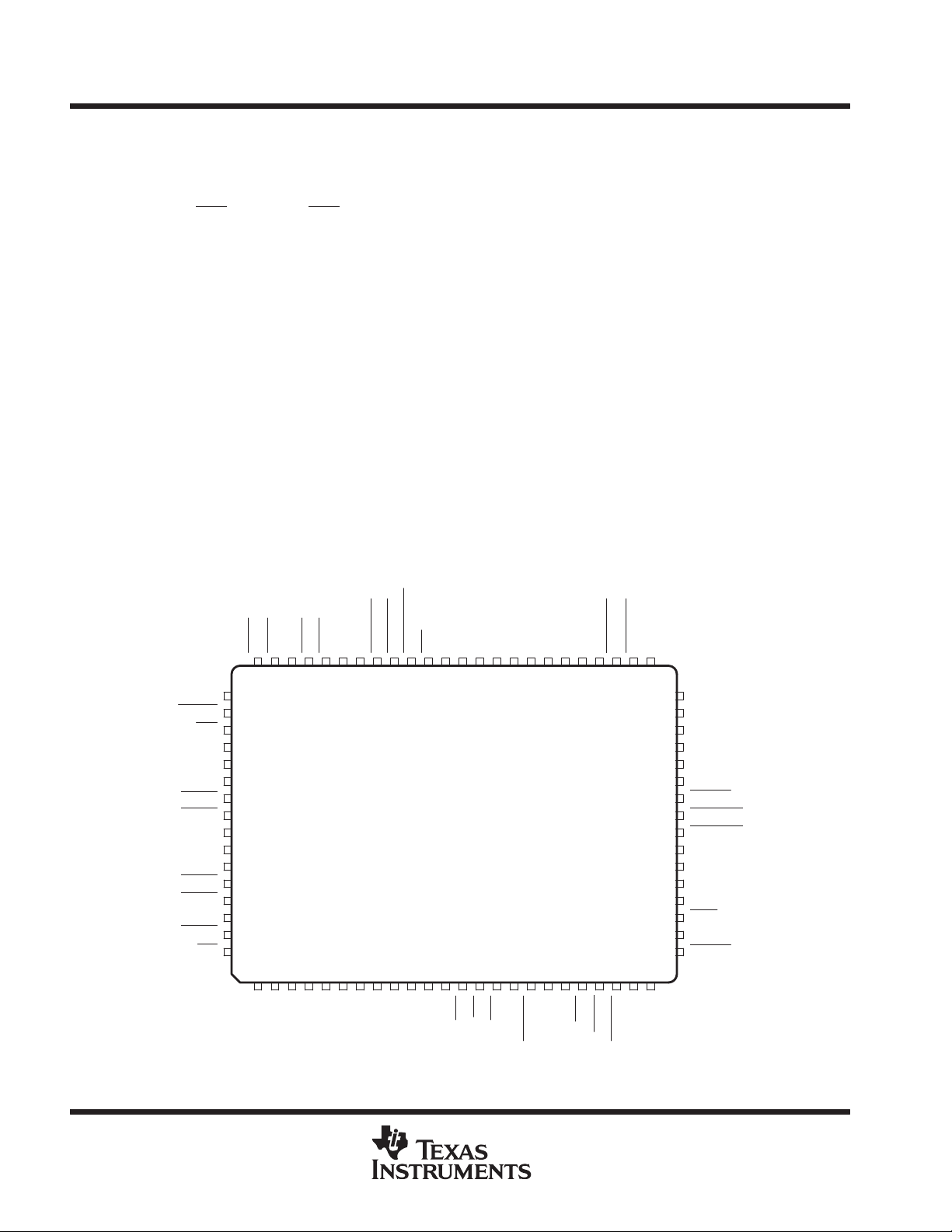
PH PACKAGE
(TOP VIEW)
CC
RTS0
CTS0
DSR0
V
64 63 62 61 6059 58 57 5655 5453 52 51 50 49 48 4746 45 4443 4241
RI0
CC
RI1
65
66
67
68
69
70
71
72
73
74
75
76
77
78
79
80
1 2 3 4 5 6 7 8 9 10 11 12 13 14 15 16 17 1819 20 2122 2324
D7D6D5
D4
IRSIN0
DCD0
SIN0
GND
SOUT1
DTR1
RTS1
CLK_OUT1
V
SIN1
DSR1
DCD1
IRSIN1
CTS1
IBM and PC/AT are trademarks of International Business Machines Corporation.
CC
SOUT0
DTR0
V
D3D2D1
STROBE
AUTOFD
D0
GND
GND
INIT
SELECTIN
A0A1A2
PD0
IOW
PD1
IOR
PD2
CS0
PD3
TC
PD5
PD4
GND
CC
V
RESET
PDACK
PD6
CS1
RXRDY1
PD7
PPCS
ECPCS
INTRPT1
RXRDY0
40
39
38
37
36
35
34
33
32
31
30
29
28
27
26
25
SELECT
PERROR
INTRPT0
IOCHRDY
BDO
V
CC
CLK_OUT0
PDRQ
PINTR
TXRDY1
TXRDY0
XOUT
GND
XIN
TEST
ACK
BUSY
FAULT
2
POST OFFICE BOX 655303 • DALLAS, TEXAS 75265
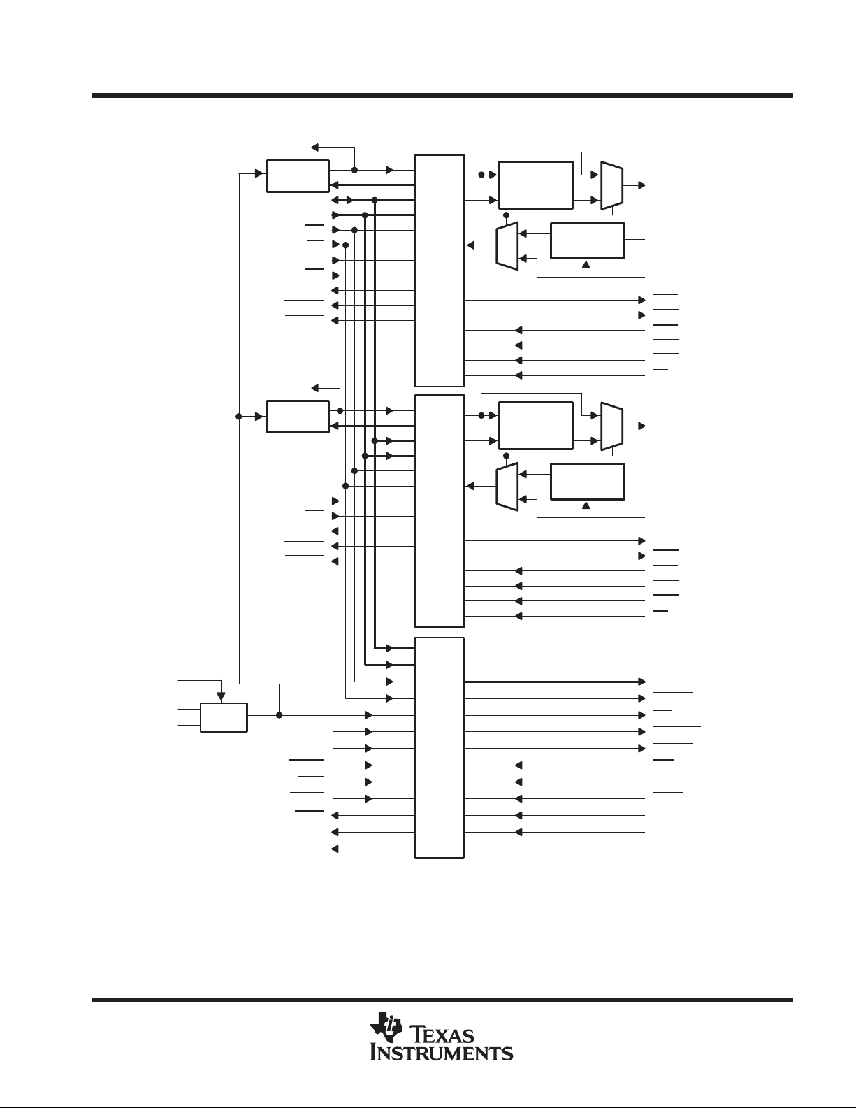
functional block diagram
TL16PIR552
DUAL UART WITH DUAL IrDA AND
1284 PARALLEL PORT
SLLS222A – DECEMBER 1995 – REVISED AUGUST 1996
CLK_OUT0
prescaler
# 0
D7–D0
A2–A0
RESET
INTRPT0
RXRDY0
TXRDY0
CLK_OUT1
prescaler
# 1
RESET
INTRPT1
RXRDY1
TXRDY1
IOW
IOR
CS0
CS1
36
73
1–8
12–10
13
14
19
15
40
42
32
19
20
41
43
33
UART 0
UART 1
61
60
63
64
66
67
72
71
79
76
77
80
IR Encoder
and
Transmit
M
U
X
IR Incoder
and
Transmit
M
U
X
IR Decoder
Receiver
IR Decoder
Receiver
M
59
U
X
M
U
X
65
68
70
78
75
SOUT0
IRSIN0
SIN0
RTS0
DTR0
CTS0
DSR0
DCD0
RI0
SOUT1
IRSIN1
SIN1
RTS1
DTR1
CST1
DSR1
DCD1
RI1
28
TEST
29
XIN
XOUT
31
22 MHz
RESET
TC
PDACK
PPCS
ECPCS
PINTR
PDRQ
IOCHRDY
NOTE A: Terminal numbers shown are for the PH package.
POST OFFICE BOX 655303 • DALLAS, TEXAS 75265
19
16
17
21
22
34
35
39
1284
Port
44–47, 49–52
57
54
55
56
27
26
25
23
24
PD7–PD0
AUTOFD
INIT
SELECTIN
STROBE
ACK
BUSY
FAULT
PERROR
SELECT
3
TL16PIR552
I/O
DESCRIPTION
DUAL UART WITH DUAL IrDA AND
1284 PARALLEL PORT
SLLS222A – DECEMBER 1995 – REVISED AUGUST 1996
Terminal Functions
TERMINAL
NAME NO.
A0–A2 10–12 I Register select. A0–A2 are address lines that select the internal registers in the device.
ACK 27 I Data acknowledge. In compatibility mode ACK is pulled low by the peripheral device to acknowledge
AUTOFD 57 O Autofeed. In compatibility mode AUTOFD is set low in conjunction with SELECTIN being set high to request
BDO 38 O Bus buffer output. BDO output is active (high) when the CPU is not reading data. It controls the system bus
BUSY 26 I Busy. In compatibility mode BUSY is driven high to indicate that the peripheral is not ready to receive data.
CLK_OUT0,
CLK_OUT1
CS0, CS1 15,20 I Chip select. CS0 and CS1 are active low inputs that act as an enable for the write operation and a read
CTS0,
CTS1
D7–D0 1–8 I/O Data bus. Eight data lines with 3-state outputs provide a bidirectional path for data, control, and status
DCD0,
DCD1
DSR0,
DSR1
DTR0,
DTR1
ECPCS 22 I Chip select. ECPCS is used for the ECP parallel port internal registers, and is an active low signal.
NOTE 1: All parallel port control outputs are open drain outputs in the Centronics mode, and push-pull outputs in other modes.
36, 73 O Prescaler Outputs. CLK_OUT0 and CLK_OUT1 drive the UARTs.
63
79
66
77
64
76
60
71
transfer of a data byte from the host. In ECP mode, ACK
AUTOFD
to indicate data is available. In EPP mode, ACK
signal is active high and is positive-edge triggered.
a 1284 mode. Then AUTOFD
low. In EPP mode, AUTOFD is an active low output that is used to denote data read or write operations.
It also provides a ninth data bit that is used to determine whether address or data information is present
on the data lines in the forward mode. In EPP mode this signal is active low to denote data read or write
operations. In ECP mode, AUTOFD
handshaking with ACK
lines contain the ECP address or data. The host drives this signal to flow control in the reverse direction.
It is an “interlocked” handshake with ACK
phase.
driver.
In the ECP mode, BUSY is driven high to indicate that the peripheral is not ready to receive data and is
driven low to indicate that the peripheral is ready to receive data in forward mode. In reverse mode, BUSY
is low when the information on the data lines are commands (RLE) and it is high when the information on
the data lines is data. In EPP mode, BUSY is active low. It is driven inactive as a positive acknowledgment
from the peripheral device that data or address information is completed. It is active when the peripheral
is ready for the next data and address transfer. In ECP mode, BUSY deasserts to indicate that the peripheral
can accept data. It handshakes with STROBE
indicates whether the data lines contain the ECP command information or data. The peripheral uses this
signal to control flow in the forward direction. It is an “interlocked” handshake with STROBE
provides command information in the reverse direction.
operation for the UART. CS0
I Clear to send. CTS0 and CTS1 are modem-status signals whose condition can be verified by reading bit
4 (CTS) of the MSR. Bit 0 (∆CTS) of the MSR indicates that CTS0
last read operation from the MSR. When the modem-status interrupt is enabled, CTS0
states, and an interrupt is generated. CTS0
transmitter.
information between the CPU and the device.
I Data carrier detect. DCD0 and DCD1 are modem status signals whose condition can be verified by reading
bit 7 (DCD) of the modem status register (MSR). Bit 3 (∆DCD) of the MSR indicates that DCD0
has changed state since the last read from MSR. If the modem status interrupt is enabled when DCD0 or
DCD1
I Data set ready. DSR0 and DSR1 are modem status signals whose condition can be verified by reading bit
5 (DSR) of the MSR. Bit 1 (∆DSR) of the MSR indicates that DSR0
last read from MSR. If the modem status interrupt is enabled when DSR0
interrupt is generated.
O Data terminal ready . When active, (low), DTR0 or DTR1 informs a modem or data set that the UART is ready
to establish communication. DTR0
register (MCR) to 1. DTR
loop-mode operation, or resetting bit 0 of the MCR.
to transfer data from the peripheral device to the host. It is asserted low by the peripheral device
is used by the peripheral device to interrupt the host. This
is set high after the peripheral device acknowledges the signal by setting ACK
requests a byte of data from the peripheral when asserted,
in the reverse direction. In the forward direction AUTOFD indicates whether the data
. AUTOFD also provides command information in the forward
enables UART0 and CS1 enables UART1.
or CTS1 is also used in the auto-CTS mode to control the
changes state, an interrupt is generated.
or DTR1 is placed in the active state by setting bit 0 of the modem-control
x is placed in the inactive state either as a result of a master reset, during
is used in a closed loop handshake with the host
in the forward direction. In the reverse direction BUSY
. BUSY also
or CTS1 has changed states since the
or CTS1 changes
or DCD1
or DSR1 has changed state since the
or DSR1 changes state, an
4
POST OFFICE BOX 655303 • DALLAS, TEXAS 75265
I/O
DESCRIPTION
TL16PIR552
DUAL UART WITH DUAL IrDA AND
1284 PARALLEL PORT
SLLS222A – DECEMBER 1995 – REVISED AUGUST 1996
Terminal Functions
TERMINAL
NAME NO.
FAULT 25 I Fault indication. In compatibility mode FAULT is set high to acknowledge the 1284 mode requested. The
GND 9, 30,
INIT 54 O Initiation. In compatibility mode INIT is pulsed low to reset the interface and force a return to the compatibility
INTRPT0,
INTRPT1
IOCHRDY 39 O ISA channel ready. IOCHRDY is an open drain output that extends the length of a bus cycle when it is
IOR 14 I Read input. IOR is an active low input signal that enables the selected channel to output data to D7–D0.
IOW 13 I Write input. IOW is an active low input signal that enables the data to be input to either a UART or to the
IRSIN0, IRSIN1 65, 78 I Serial data. IRSIN0 and IRSIN1 are serial inputs from an IR serial data communication device.
PD0–PD7 52–49,
PDACK 17 I Parallel port DMA acknowledge. PDACK is an active low input.
PDRQ 35 O DMA Request. PDRQ is used for parallel port DMA requests during ECP and FIFO modes.
PERROR 23 I Peripheral error. In compatibility mode PERROR is driven high when the device encounters an error in the
PINTR 34 O Parallel port interrupt. PINTR is a 3-state output. In EPP mode this is an active high, positive-edge triggered
PPCS 21 I Chip select. PPCS is used for the parallel port internal registers and is an active-low signal.
RI0,
RI1
RESET 19 I Reset. RESET is an active high reset that when asserted, clears all UART s and parallel port printer internal
RTS0,
RTS1
NOTE 1: All parallel port control outputs are open drain outputs in the Centronics mode, and push-pull outputs in other modes.
48, 53,
69
40,41 O Interrupt (0–1). When active (high), INTRPT0 or INTRPT1 informs the CPU that the UART has an interrupt
47–44
67,80 I Ring Indicator. RI0 and RI1 are modem-status signals whose condition can be verified by reading bit 6 (RI)
61
72
EPP mode is user defined. In ECP mode FAULT
a mechanism for peer-to-peer communication. This signal is valid only in the forward direction. During ECP
mode the peripheral is permitted (but not required) to drive this terminal low to request a reverse transfer.
The request is merely a “hit” to the host; the host has ultimate control over the transfer direction. FAULT
is typically used to generate an interrupt to the host CPU.
Ground terminal.
mode idle phase.In ECP mode INIT
the peripheral to drive the bidirectional data lines when SELECTIN
When driven low, this signal initiates a termination cycle that results in the interface returning to the
compatibility mode.
to be serviced. Four conditions that cause an interrupt to be issued include a receiver error, received data
is available, an empty transmitter holding register, or an enabled modem-status interrupt.
inactive.
The data output depends upon the register selected by the address A2–A0 inputs and chip select.
parallel port. The data destination depends upon the register selected by the address inputs A2–A0 and
chip select.
I/O Parallel data bits (0–7). PD0–PD7 provide a byte wide input or 47–44 output port to the system. These bits
contain address, data, or RLE command data.
paper path. In ECP mode the peripheral drives PERROR low to acknowledge a reverse request (INIT
Based on this signal the host determines when it is permitted to drive the data bus. In EPP mode the signal
is user defined.
input.
of the MSR. Bit 2 (TERI) of the MSR indicates that the RI0
level since the last read operation from MSR. If the modem-status interrupt is enabled when this transition
occurs, an interrupt is generated.
registers.
O Request to send. When active, RTS0 or RTS1 informs the modem or data set that the UART is ready to
receive data. RTS0
set to inactive (high) either as a result of master reset or during loop-mode operations or by resetting bit
1 (RTS) of the MCR. In the auto-RTS
logic.
or RTS1 is set to its active level by setting the RTSx modem-control register bit and is
is driven low to place the channel in the reverse direction and it allows
mode, RTSx is set to its inactive level by the receiver threshold-control
generates an error interrupt when asserted. It provides
is high. In EPP mode INIT is active low.
/RI1 input has transitioned from a low to a high
).
POST OFFICE BOX 655303 • DALLAS, TEXAS 75265
5
TL16PIR552
I/O
DESCRIPTION
DUAL UART WITH DUAL IrDA AND
1284 PARALLEL PORT
SLLS222A – DECEMBER 1995 – REVISED AUGUST 1996
Terminal Functions
TERMINAL
NAME NO.
RXRDY0,
RXRDY1
SELECT 24 I Select. In compatibility mode SELECT is set high to indicate that the printer is on line. In ECP mode SELECT
SELECTIN 55 O Select. In compatibility mode SELECTIN is set low by the host to select the peripheral device. It is set high
SIN0, SIN1 68,75 I Serial data. SIN0 and SIN1 are inputs from a connected communication device.
SOUT0,
SOUT1
STROBE 56 O Data strobe. In compatibility mode STROBE is set active low to transfer data into the input latch of the
TC 16 I T erminal count. TC is an active high input during DMA and when PDACK is low . TC indicates that the data
TEST 28 I T est. TEST is tied low during normal operation. To turn the oscillator of f and measure ICCQ current, TEST
TXRDY0,
TXRDY1
V
CC
XIN
XOUT
NOTE 1: All parallel port control outputs are open drain outputs in the Centronics mode, and push-pull outputs in other modes.
42,43 O Receiver ready . Receiver direct-memory access (DMA) signaling is available with RXRDY0 or RXRDY1.
59, 70 O Serial outputs. Either IR output format or UART output format. Composite serial data outputs are to be
32,33 O Transmitter ready. Transmitter DMA signaling is available with TXRDY0 and TXRDY1. When operating in
18, 37,
58 62,
74
2931I/O Crystal input and output terminals. A 22-MHz clock is required to meet the internal timing required by the
When operating in the FIFO mode, one of two types of DMA signalling can be selected using the FIFO
control-register bit 3 (FCR3). When operating in the TL16C450 mode, only DMA mode 0 is allowed. Mode
0 supports single-transfer DMA in which a transfer is made between CPU bus cycles. Mode 1 supports
multitransfer DMA in which multiple transfers are made continuously until the receiver FIFO has been
emptied. In DMA mode 0 (FCR0 = 0 or FCR0 = 1, FCR3 = 0), if there is at least one character in the receiver
FIFO or receiver holding register, RXRDY0
but there are no characters in the FIFO or holding register, RXRDYx
(FCR0 = 1, FCR3 = 1), when the trigger level or the timeout has been reached, RXRDYx
when it has been active but there are no more characters in the FIFO or holding register, it goes inactive
(high).
indicates an affirmative response for each extensibility byte. It is high when the requested mode is
supported. In EPP mode the signal is user defined.
to request the 1284 mode. In ECP mode SELECTIN
to terminate the ECP mode and return to the compatibility mode. In EPP mode SELECTIN
output that is used to denote address read or write operations.
connected to a communication device. SOUT0 and SOUT1 are set to the marking state (1) as a result of
a master reset operation.
peripheral device. Data is valid while STROBE
handshake with BUSY to transfer data or address information from the host to the peripheral device. In EPP
mode this signal is set low to denote an address or data write operation to the peripheral and is set high
to denote and address or data read operation from the peripheral.
transfer is complete.
is tied active (high).
the FIFO mode, one of two types of DMA signalling can be selected through FCR3. When operating in the
TL16C450 mode, only DMA mode 0 is allowed. Mode 0 supports single-transfer DMA in which a transfer
is made between the CPU bus cycles. Mode 1 supports multitransfer DMA in which multiple DMA transfers
are made continuously until the transmit FIFO has been filled.
5-V supply voltage.
1284 parallel port (minimum 40 to 60% duty cycle).
and RXRDY1 are active (low). When RXRDYx has been active
goes inactive (high). In DMA mode 1
goes active (low);
is driven high by the host. It is driven low by the host
is an active low
is low. In ECP mode STROBE is used in a closed-loop
detailed description
autoflow control
Autoflow control is comprised of auto-CTS
the transmitter FIFO can emit data (see Figure 1). With auto-RTS
needs more data and notifies the sending serial device (see Figure 1). When RTSx
transmission does not occur unless the receiver FIFO has space for the data; thus, overrun errors are eliminated
when UART1 and UART2 are TL16PIR552s with enabled autoflow control. If not, overrun errors occur when
the transmit-data rate exceeds the receiver FIFO read latency.
6
POST OFFICE BOX 655303 • DALLAS, TEXAS 75265
and auto-RTS. With auto-CTS, the CTSx input must be active before
, RTSx becomes active when the receiver
is connected to CTSx, data
TL16PIR552
DUAL UART WITH DUAL IrDA AND
1284 PARALLEL PORT
SLLS222A – DECEMBER 1995 – REVISED AUGUST 1996
UART1 UART2
SINx SOUTx
RTSx
SOUTx SINx
CTSx
CTSx
RTSx
Parallel
to Serial
XMT
FIFO
Flow
Control
Serial to
Parallel
RCV
FIFO
Flow
Control
D7–D0
RCV
FIFO
XMT
FIFO
Serial to
Parallel
Flow
Control
Parallel
to Serial
Flow
Control
Figure 1. Autoflow Control (Auto-RTS and Auto-CTS) Example
auto-RTS (see Figure 1)
Auto-RTS
data-flow control originates in the receiver timing and control block (see functional block diagram)
and is linked to the programmed receiver-FIFO trigger level. When the receiver-FIFO level reaches a trigger
level of 1, 4, or 8 (see Figure 3), RTSx
is deasserted. With trigger levels of 1, 4, and 8, the sending UART may
send an additional byte after the trigger level is reached (assuming the sending UART has another byte to send)
because it may not recognize the deassertion of RTSx
until after it has begun sending the additional byte. RTSx
is automatically reasserted once the receiver (RCV) FIFO is emptied by reading the receiver buffer
register(RBR).
If the trigger level is 14 (see Figure 6), RTSx
present on the SINx line. RTSx
is reasserted when the RCV FIFO has at least one available byte space.
is deasserted after the first data bit of the sixteenth character is
D7–D0
auto-CTS
(see Figure 1)
The transmitter circuitry checks CTSx
byte. To stop the transmitter from sending the following byte, CTSx
before sending the next data byte. When CTSx is active, it sends the next
must be released before the middle of the
last stop bit that is currently being sent (see Figure 2). The auto-CTS
system. When flow control is enabled, the CTSx
automatically controls its own transmitter. Without auto-CTS
level changes do not trigger host interrupts because the device
, the transmitter sends any data present in the
function reduces interrupts to the host
transmit FIFO and a receiver overrun error may result.
enabling autoflow control and auto-CTS
Autoflow control is enabled by setting modem-control register (MCR) bit 5 (autoflow enable or AFE) and bit 1
(RTS) to 1. Autoflow incorporates both auto-RTS
MCR should be reset to 0 (this assumes a control signal is driving CTSx
auto-CTS
SOUTx
CTSx
NOTE A: When CTSx is low, the transmitter keeps sending serial data out. When CTSx goes high before the middle of the last stop bit of the current
and auto-RTS functional timing
Start Bits 0–7 Start Bits 0–7 Start Bits 0–7
byte, the transmitter finishes sending the current byte but it does not send the next byte. When CTSx
begins sending data again.
Stop Stop Stop
and auto-CTS. When only auto-CTS is desired, bit 1 in the
).
goes from high to low, the transmitter
Figure 2. CTS Functional Timing
POST OFFICE BOX 655303 • DALLAS, TEXAS 75265
7
TL16PIR552
DUAL UART WITH DUAL IrDA AND
1284 PARALLEL PORT
SLLS222A – DECEMBER 1995 – REVISED AUGUST 1996
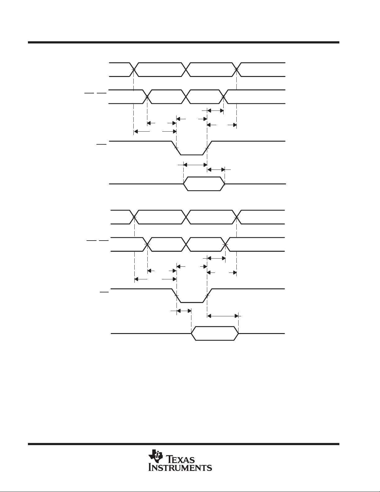
The receiver-FIFO trigger level can be set to 1, 4, 8, or 14 bytes. These are described in Figures 3 and 4.
SINx
RTSx
IOR
(IOR RBR)
NOTES: A. N = RCV-FIFO trigger level (1, 4, or 8 bytes)
B. The two blocks in dashed lines cover the case where an additional byte is sent as described in the preceding
Start Byte N Start Byte N+1 Start Byte
Stop Stop Stop
12
N N+1
auto-RTS
section.
Figure 3. RTS Functional Timing, RCV-FIFO Trigger Level = 1,4, or 8 Bytes
SINx
RTSx
IOR
(IOR RBR)
NOTE A: RTSx is deasserted when the receiver receives the first data bit of the sixteenth byte. The receive FIFO is full after finishing the sixteenth
byte. RTSx
than one byte of space available. When the receive FIFO is full, the first receive buffer-register read reasserts RTSx
Byte 14 Byte 15
RTS Released After the
First Data Bit of Byte 16
is asserted again when there is at least one byte of space available and no incoming byte is in processing or there is more
Start Byte 18 StopStart Byte 16 Stop
.
Figure 4. RTS Functional Timing, Receiver - FIFO Trigger Level = 14 Bytes
absolute maximum ratings over operating free-air temperature range (unless otherwise noted)
Supply voltage range, V
Input voltage range, V
Output voltage range, V
Input clamp current, I
Output clamp current, I
Output clamp current, level shift, I
Virtual junction, T
150°C. . . . . . . . . . . . . . . . . . . . . . . . . . . . . . . . . . . . . . . . . . . . . . . . . . . . . . . . . . . . . . . . . . . . . . .
J
Storage temperature range, T
†
Stresses beyond those listed under “absolute maximum ratings” may cause permanent damage to the device. These are stress ratings only, and
functional operation of the device at these or any other conditions beyond those indicated under “recommended operating conditions” is not
implied. Exposure to absolute-maximum-rated conditions for extended periods may affect device reliability.
NOTES: 2. This applies to external input and bidirectional buffers. VI < VCC does not apply to fail-safe terminals.
3. This applies to external output and bidirectional buffers. VO < VCC does not apply to fail-safe terminals.
–0.5 V to 6 V. . . . . . . . . . . . . . . . . . . . . . . . . . . . . . . . . . . . . . . . . . . . . . . . . . . . . . . . . .
CC
–0.5 V to V
I
–0.5 V to V
O
(V
IK
OK
< 0 or V
I
(V
O
> VCC) (See Note 2) ±20 mA. . . . . . . . . . . . . . . . . . . . . . . . . . . . . . . . . . . .
I
< 0 or V
OK
–65°C to 150°C. . . . . . . . . . . . . . . . . . . . . . . . . . . . . . . . . . . . . . . . . . . . . . . . . . .
stg
> VCC) (See Note 3) ±20 mA. . . . . . . . . . . . . . . . . . . . . . . . . . . . . . . .
O
(V
< 0 or V
O
> VCC) (See Note 3) ±20 mA. . . . . . . . . . . . . . . . . . . . . . .
O
CC
CC
+ 0.5 V. . . . . . . . . . . . . . . . . . . . . . . . . . . . . . . . . . . . . . . . . . . . . . . . . . . . . .
+ 0.5 V. . . . . . . . . . . . . . . . . . . . . . . . . . . . . . . . . . . . . . . . . . . . . . . . . . .
†
8
POST OFFICE BOX 655303 • DALLAS, TEXAS 75265
PARAMETER
TEST CONDITIONS
UNIT
TL16PIR552
DUAL UART WITH DUAL IrDA AND
1284 PARALLEL PORT
SLLS222A – DECEMBER 1995 – REVISED AUGUST 1996
recommended operating conditions
MIN NOM MAX UNIT
Supply voltage, V
Input voltage, V
High-level input voltage, V
Low-level input voltage, V
Input transition (rise and fall) time, t
Operating ambient temperature range, T
Virtual junction temperature, T
CC
I
IH
IL
t
A
J
electrical characteristics over recommended ranges of supply voltage and operating free-air
temperature (unless otherwise noted)
V
OH
V
OL
V
IT+
V
IT–
V
hys
I
OZ
I
IL
I
IH
†
12 mA for 1284 control, 3 mA for all other outputs
‡
Applies to external input and bidirectional buffers with hysteresis. All input buffers have hysteresis.
§
A 3-state or open-drain output must be in the high-impedance state.
NOTE 4: All 1284 output and data terminals are low-noise TTL 12 mA drivers. The type of the driver, push/pull or open drain, is switched
High-level output voltage IOH = Rated
Low-level output voltage IOL = Rated
Positive-going input threshold voltage
Negative-going input threshold voltage
Hysteresis‡ (V
3-state-output Hi-Z current VI = VCC or GND
Low-level input current VI = GND –1 µA
High-level input current VI = V
dynamically based on the 1284 mode.
IT+
– V
) TTL compatible 0.25 0.7 V
IT–
‡
‡
TTL compatible 2 V
TTL compatible 0.8 V
†
†
CC
4.75 5 5.25 V
0 V
2 V
–0.5 0.8 V
0 25 ns
0 25 70 °C
0 25 115 °C
COMMERCIAL
MIN MAX
VCC –0.8 V
§
CC
CC
0.5 V
±10 µA
1 µA
V
V
POST OFFICE BOX 655303 • DALLAS, TEXAS 75265
9
TL16PIR552
DUAL UART WITH DUAL IrDA AND
1284 PARALLEL PORT
SLLS222A – DECEMBER 1995 – REVISED AUGUST 1996
system timing requirements over recommended ranges of supply voltage and operating free-air
temperature
ALT. SYMBOL FIGURE TEST CONDITIONS MIN MAX UNIT
t
Cycle time, read (tw7 + td8) RC 65 ns
cR
t
Cycle time, write (tw6 + td5) WC 59 ns
cW
t
Pulse duration, IOW t
w1
t
Pulse duration, IOR t
w2
t
Pulse duration, RESET t
w3
t
Setup time, data valid before IOW↑ t
su1
t
Setup time, CTS↑ before midpoint of stop bit 16 10 ns
su2
t
Hold time, CS valid after IOW↑ t
h1
t
Hold time, address valid after IOW↑ t
h2
t
Hold time, data valid after IOW↑ t
h3
t
Hold time, chip select valid after IOR↑ t
h4
t
Hold time, address valid after IOR↑ t
h5
t
Delay time, CS valid before IOW↓ t
d1
t
Delay time, address valid before IOW↓ t
d2
t
Delay time, CS valid to IOR↓ t
d3
t
Delay time, address valid to IOR↓ t
d4
t
Delay time, IOR↓ to data valid t
d5
t
Delay time, IOR↑ to floating data t
d6
WR
RD
MR
DS
WCS
WA
DH
RCS
RA
CSW
AW
CSR
AR
RVD
HZ
5 50 ns
6 50 ns
1 µs
5 20 ns
5 15 ns
5 15 ns
5 15 ns
6 20 ns
6 20 ns
5 10 ns
5 13 ns
6 10 ns
6 13 ns
6 CL = 75 pF 20 ns
6 CL = 75 pF 10 ns
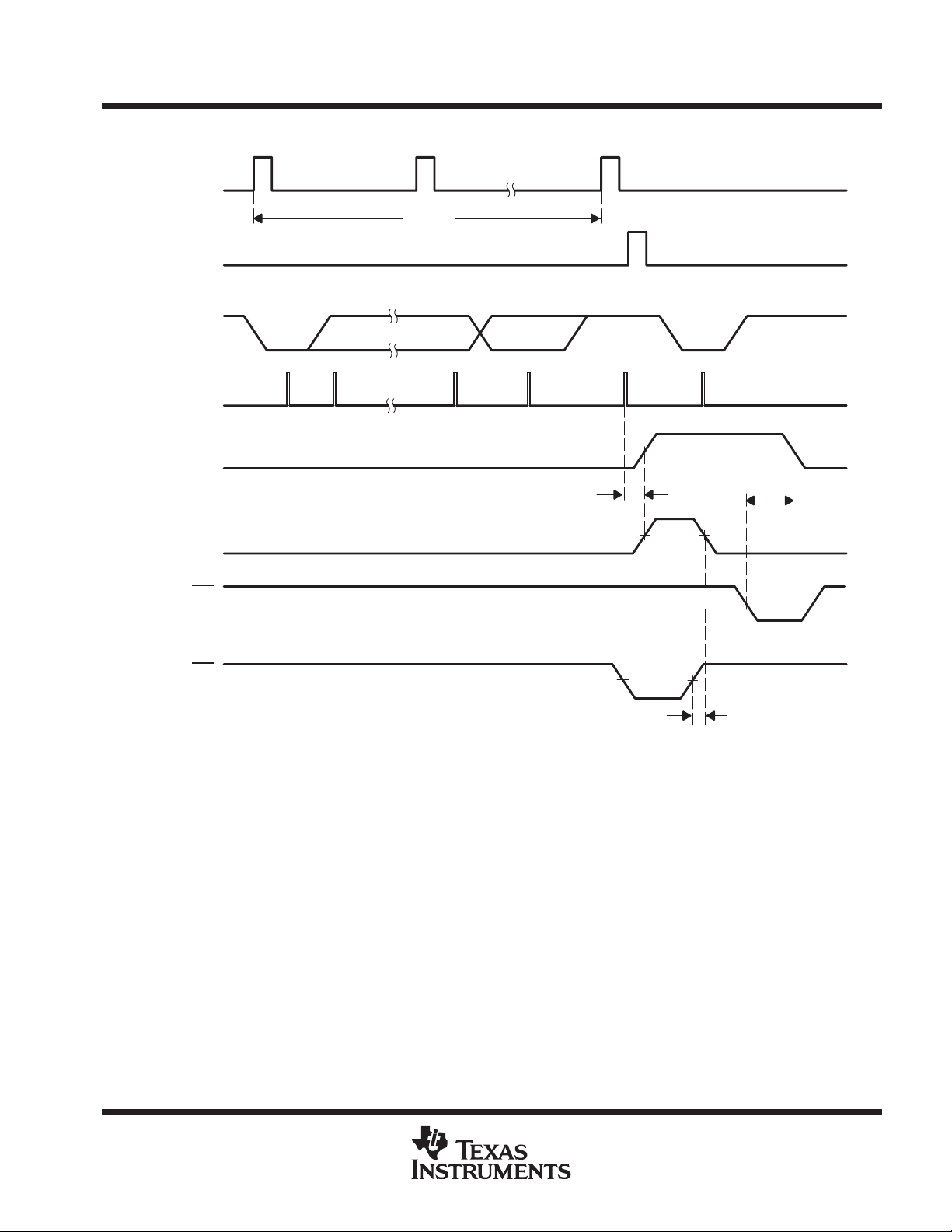
receiver switching characteristics over recommended ranges of supply voltage and operating
free-air temperature (see Note 5)
PARAMETER ALT. SYMBOL FIGURE TEST CONDITIONS MIN MAX UNIT
Delay time, stop to INTRPTx↑ or read RBR↑ to
t
d7
LSI INTRPT↑ or stop to RXRDY
Delay time, read RBR/INTRPT or read to RXRDY↑
t
d8
or IOR
↑ to INTRPTx↓
NOTE 5: In the FIFO mode, the read cycle (RC) = 425 ns (min) between reads of the receive FIFO and the status registers (interrupt-
identification register or line-status register).
↓
t
SINT
t
RINT
7, 8, 9,
10, 11
7, 8, 9,
10, 11
RCLK
1
cycle
CL = 75 pF 70 ns
10
POST OFFICE BOX 655303 • DALLAS, TEXAS 75265
TL16PIR552
DUAL UART WITH DUAL IrDA AND
1284 PARALLEL PORT
SLLS222A – DECEMBER 1995 – REVISED AUGUST 1996
transmitter switching characteristics over recommended ranges of supply voltage and operating
free-air temperature
PARAMETER ALT. SYMBOL FIGURE TEST CONDITIONS MIN MAX UNIT
baud-
t
Delay time, INTRPTx↓ to SOUTx↓ t
d9
t
Delay time, start to INTRPTx↑ t
d10
t
Delay time, IOW↑ to INTRPTx↓ t
d11
t
Delay time, IOW↓ to INTRPTx↑ t
d12
t
Delay time, IOR IIR↓ to INTRPTx↓ t
d13
t
Delay time, IOW↑ to TXRDYx↑ t
d14
t
Delay time, SOUTx↓ to TXRDYx↓
d15
†
THRE = transmitter holding-register empty; IIR = interrupt-identification register.
IRS
STI
HR
WXI
t
SXA
SI
IR
12 8 24
12 8 10
12 CL = 75 pF 50 ns
12 16 34
12 CL = 75 pF 35 ns
13,14 CL = 75 pF 30 ns
13, 14 CL = 75 pF 9
modem-control switching characteristics over recommended ranges of supply voltage and
= 75 pF
operating free-air temperature, C
PARAMETER ALT. SYMBOL FIGURE MIN MAX UNIT
t
Delay time, CTSx, DSRx, DCDx↓ to INTRPTx↑ or RI↑ to INTRPTx↑ t
d16
t
Delay time, IOR↑ to INTRPTx↓ 15 24
d17
t
Delay time, CTSx↓ to SOUTx↓ 16 2
d18
t
Delay time, midpoint of stop bit to RTSx↑ 17 2
d19
t
Delay time, IOR↓ to RTSx↓ 17 2
d20
t
Delay time, first data bit of the sixteenth character to RTSx↑ 18 2
d21
t
Delay time, IOR↓ to RTSx↓ t
d22
t
Delay time, IOW↑ to RTSx, DTRx↑↓ t
d23
L
RIM
MDO
SIM
15 35 ns
18 40 ns
15 35 ns
out
cycles
baud-
out
cycles
baud-
out
cycles
baud-
out
cycles
baudout
cycles
baudout
cycles
baudout
cycles
baudout
cycles
baudout
cycles
IR signal switching characteristics over recommended ranges of supply voltage and operating
free-air temperature, C
t
Delay time, internal SOUTx↓ to SOUTx↑ (IR mode) 19 8
d24
t
Delay time, incoming IRSINx↑ to internal SINx↓ 19 15 ns
d25
= 75 pF
L
PARAMETER ALT. SYMBOL FIGURE MIN MAX UNIT
baud-
out
cycles
parallel-port timing requirements over recommended ranges of supply voltage and operating
free-air temperature
PARAMETER FIGURE MIN MAX UNITS
t
d26
t
d27
t
w4
Delay time, FAULT↓ to PINTR (ECP)↓ 20 20 ns
Delay time, ACK↓ to PINTR (EPP)↓ 20 20 ns
Pulse duration, PINTR (ECP)↓ to PINTR (ECP)↑ (ECP and EPP modes) 20 80 100 ns
POST OFFICE BOX 655303 • DALLAS, TEXAS 75265
11
TL16PIR552
DUAL UART WITH DUAL IrDA AND
1284 PARALLEL PORT
SLLS222A – DECEMBER 1995 – REVISED AUGUST 1996
parallel-port EPP data or address write cycle timing requirements over recommended ranges of
supply voltage and operating free-air temperature
PARAMETER FIGURE MIN MAX UNITS
t
h6
t
d28
t
d29
t
d30
t
d31
t
d32
t
d33
t
d34
t
d35
t
d36
t
d37
t
d38
t
d39
Hold time, BUSY↓ to PD invalid 21 60 140 ns
Delay time, IOW↓ to PD valid 21 10 30 ns
Delay time, BUSY↓ to STROBE↑ 21 60 100 ns
Delay time, STROBE↓ to AUTOFD↓ 21 0 10 ns
Delay time, BUSY↑ to AUTOFD↑ 21 60 100 ns
Timeout, IOW↓ to BUSY↑ 21 10 12 µs
Delay time, SELECTIN↑ to BUSY↓ 21 200 ns
Delay time, IOW↓ to IOCHRDY↓ 21 0 25 ns
Delay time, BUSY↑ to IOCHRDY↑ 21 60 120 ns
Delay time,
Delay time, IOW↓ to STROBE↓ 21 0 40 ns
Delay time, IOW↑ to IOW or IOR↓ 21 60 ns
Delay time, BUSY↓ to STROBE↓ 21 20 40 ns
IOCHRDY
↑ to IOW↑ 21 30 ns
parallel-port EPP data or adress read cycle timing requirements over recommended ranges of
supply voltage and operating free-air temperature
PARAMETER FIGURE MIN MAX UNITS
t
h7
t
h8
t
d40
t
d41
t
d42
t
d43
t
d44
t
d45
t
d46
t
d47
Hold time, AUTOFD, SELECTIN↑ to PD hi-Z 22 10 ns
Hold time, IOR↑ to D hi-Z (Hold Time) 22 0 20 ns
Delay time, BUSY↑ to AUTOFD, SELECTIN↑ 22 120 200 ns
Delay time, AUTOFD, SELECTIN↓ to PD Valid 22 110 ns
Delay time, IOR↓ to IOCHRDY↓ 22 0 25 ns
Delay time, BUSY↑ to IOCHRDY↑ 22 80 130 ns
Delay time, PD valid to D valid 22 0 25 ns
Timeout, IOR↓to BUSY↑ 22 10 12 µs
Delay time, IOR↑ to IOW or IOR↓ 22 60 ns
Delay time, IOCHRDY↑ to IOR↑ 22 30 ns
parallel-port FIFO timing requirements over recommended ranges of supply voltage and operating
free-air temperature
PARAMETER FIGURE MIN MAX UNITS
t
su3
t
h9
t
w5
t
d48
t
d49
Setup time, PD valid to STROBE↓ 23 550 ns
Hold time, PD hold from STROBE↑ 23 500 ns
Pulse duration, STROBE pulse width low 23 500 ns
Delay time, STROBE↓ to BUSY↑ active 23 125 ns
Delay time, BUSY↓ to STROBE↓ 23 600 ns
12
POST OFFICE BOX 655303 • DALLAS, TEXAS 75265
TL16PIR552
DUAL UART WITH DUAL IrDA AND
1284 PARALLEL PORT
SLLS222A – DECEMBER 1995 – REVISED AUGUST 1996
parallel-port (ECP) reverse timing requirements over recommended ranges of supply voltage and
operating free-air temperature
PARAMETER FIGURE MIN MAX UNITS
t
su4
t
d50
t
d51
t
d52
t
d53
t
d54
parallel-port (ECP) forward timing requirements over recommended ranges of supply voltage and
operating free-air temperature
t
su5
t
h10
t
d55
t
d56
t
d57
t
d58
t
d59
t
d60
Setup time, PD valid to ACK↓ 24 0 ns
Delay time, AUTOFD↓ to PD changed 24 0 ns
Delay time, ACK↑ to AUTOFD↓ 24 80 200 ns
Delay time, ACK↑ to AUTOFD↓ 24 80 120 ns
Delay time, AUTOFD↓ to ACK↓ 24 25 ns
Delay time, AUTOFD↑ to ACK↑ 24 150 ns
PARAMETER FIGURE MIN MAX UNITS
Setup time, PD valid to STROBE↓ 25 0 90 ns
Hold time, BUSY↓ to PD changed 25 30 180 ns
Delay time, AUTOFD valid to STROBE↓ 25 0 45 ns
Delay time, BUSY↓ to AUTOFD changed 25 25 180 ns
Delay time, STROBE↓ to BUSY↑ 25 370 ns
Delay time, STROBE↑ to BUSY↓ 25 295 ns
Delay time, BUSY↓ to STROBE↓ 25 80 120 ns
Delay time, BUSY↑ to STROBE↑ 25 20 60 ns
POST OFFICE BOX 655303 • DALLAS, TEXAS 75265
13
TL16PIR552
DUAL UART WITH DUAL IrDA AND
1284 PARALLEL PORT
SLLS222A – DECEMBER 1995 – REVISED AUGUST 1996
PARAMETER MEASUREMENT INFORMATION
A0–A2
CS0, CS1
IOW
D7–D0
A0–A2
, CS1
CS0
50%
50% 50%
Valid Valid
Valid Valid
t
h1
t
t
d1
t
d2
50% 50%
t
su1
w1
Active
Valid Data
Figure 5. Write-Cycle Timing
50%
50%
Valid Valid
Valid Valid
t
h2
50%
t
h3
50%
50%
IOR
D7–D0
t
h4
t
t
d3
t
d4
50% 50%
t
d5
w2
Active
t
h5
Valid Data
Figure 6. Read-Cycle Timing
t
d6
14
POST OFFICE BOX 655303 • DALLAS, TEXAS 75265
Sample Clock
TL16C450 Mode:
TL16PIR552
DUAL UART WITH DUAL IrDA AND
1284 PARALLEL PORT
SLLS222A – DECEMBER 1995 – REVISED AUGUST 1996
PARAMETER MEASUREMENT INFORMATION
RCLK
(Internal)
8 CLKs
SINx
Sample Clock
(Internal)
INTRPTx
(data ready)
INTRPTx
(RCV error)
IOR
(read RBR)
IOR
(read LSR)
Parity StopStart Data Bits 5–8
t
d7
Figure 7. Receiver Timing
50%
50%
Active
t
d8
50%
50%
t
d8
50%50%
Active
POST OFFICE BOX 655303 • DALLAS, TEXAS 75265
15
TL16PIR552
DUAL UART WITH DUAL IrDA AND
1284 PARALLEL PORT
SLLS222A – DECEMBER 1995 – REVISED AUGUST 1996
PARAMETER MEASUREMENT INFORMATION
SINx
Sample Clock
Trigger Level
INTRPTx
(FCR6, 7 = 0, 0)
INTRPTx
Line-Status
Interrupt (LSI)
IOR
(RD LSR)
IOR
(RD RBR)
NOTE A: For a timeout interrupt, td7 = 9 RCLKs.
Data Bits 5–8
(see Note A)
Figure 8. Receive FIFO First Byte (Sets DR Bit)
Stop
(FIFO at or above
50%
t
d7
t
d8
Active
t
50%50%
50%
50%
50%
d8
Active
trigger level)
(FIFO below
trigger level)
SINx
Sample Clock
Timeout or
Trigger Level
Interrupt
(see Note A)
Line-Status
Interrupt (LSI)
IOR
(RD LSR)
IOR
(RD RBR)
Previous Byte
Read From FIFO
NOTE A: For a timeout interrupt, td7 = 9 RCLKs.
Stop
50%
t
d7
Top Byte of FIFO
t
d7
Active Active
50% 50%
t
d8
t
d8
50%
50%50%
50%
Figure 9. Receive FIFO Bytes Other Than the First Byte (DR Internal Bit Already Set)
(FIFO at or above
trigger level)
(FIFO below
trigger level)
16
POST OFFICE BOX 655303 • DALLAS, TEXAS 75265

TL16PIR552
DUAL UART WITH DUAL IrDA AND
1284 PARALLEL PORT
SLLS222A – DECEMBER 1995 – REVISED AUGUST 1996
PARAMETER MEASUREMENT INFORMATION
IOR
(IOR RBR)
SINx
(first byte)
Sample Clock
t
(see Note A)
RXRDYx
NOTE A: For a timeout interrupt, td7 = 9 RCLKs.
d7
Figure 10. Receiver Ready (RXRDY), FCR0 = 0 or FCR0 = 1 and FCR3 = 0 (Mode 0)
IOR
(IOR RBR)
(first byte that reaches
the trigger level)
SINx
Stop
50%
50%
t
d8
50%
Active
(see Note A)
50%
Active
(see Note A)
Sample Clock
t
(see Note A)
RXRDYx
NOTES: A. This is the reading of the last byte in the FIFO.
B. For a timeout interrupt, td7 = 9 RCLKs.
d7
Figure 11. Receiver Ready (RXRDY), FCR0 = 1 or FCR3 = 1 (Mode 1)
t
d8
50%50%
POST OFFICE BOX 655303 • DALLAS, TEXAS 75265
17

TL16PIR552
DUAL UART WITH DUAL IrDA AND
1284 PARALLEL PORT
SLLS222A – DECEMBER 1995 – REVISED AUGUST 1996
PARAMETER MEASUREMENT INFORMATION
SOUTx
INTRPTx
(THRE)
IOW
(IOW THR)
IIR
IOR
Start
50%
t
d9
50% 50% 50% 50% 50%
t
d12
t
d11
50%
50%
Data Bits
50%
t
d11
Parity Stop
t
d10
Start
50%
t
d13
Figure 12. Transmitter Timing Waveforms
IOW
(WR THR)
SOUTx
Byte #1
Data
50%
Parity
Stop
Start
50%
50%
t
d15
50%
TXRDYx
t
d14
50%
Figure 13. Transmitter Ready (TXRDYx), FCR0 = 0 or FCR0 = 1 and FCR3 = 0 (Mode 0)
IOW
(IOW THR)
SOUTx
TXRDYx
Data
Byte #16
t
d14
50%
50%
Parity
Stop
t
FIFO Full
Start
50%
d15
50%
Figure 14. Transmitter Ready (TXRDYx), FCR0 = 1 and FCR3 = 1 (Mode 1)
18
POST OFFICE BOX 655303 • DALLAS, TEXAS 75265

TL16PIR552
DUAL UART WITH DUAL IrDA AND
1284 PARALLEL PORT
SLLS222A – DECEMBER 1995 – REVISED AUGUST 1996
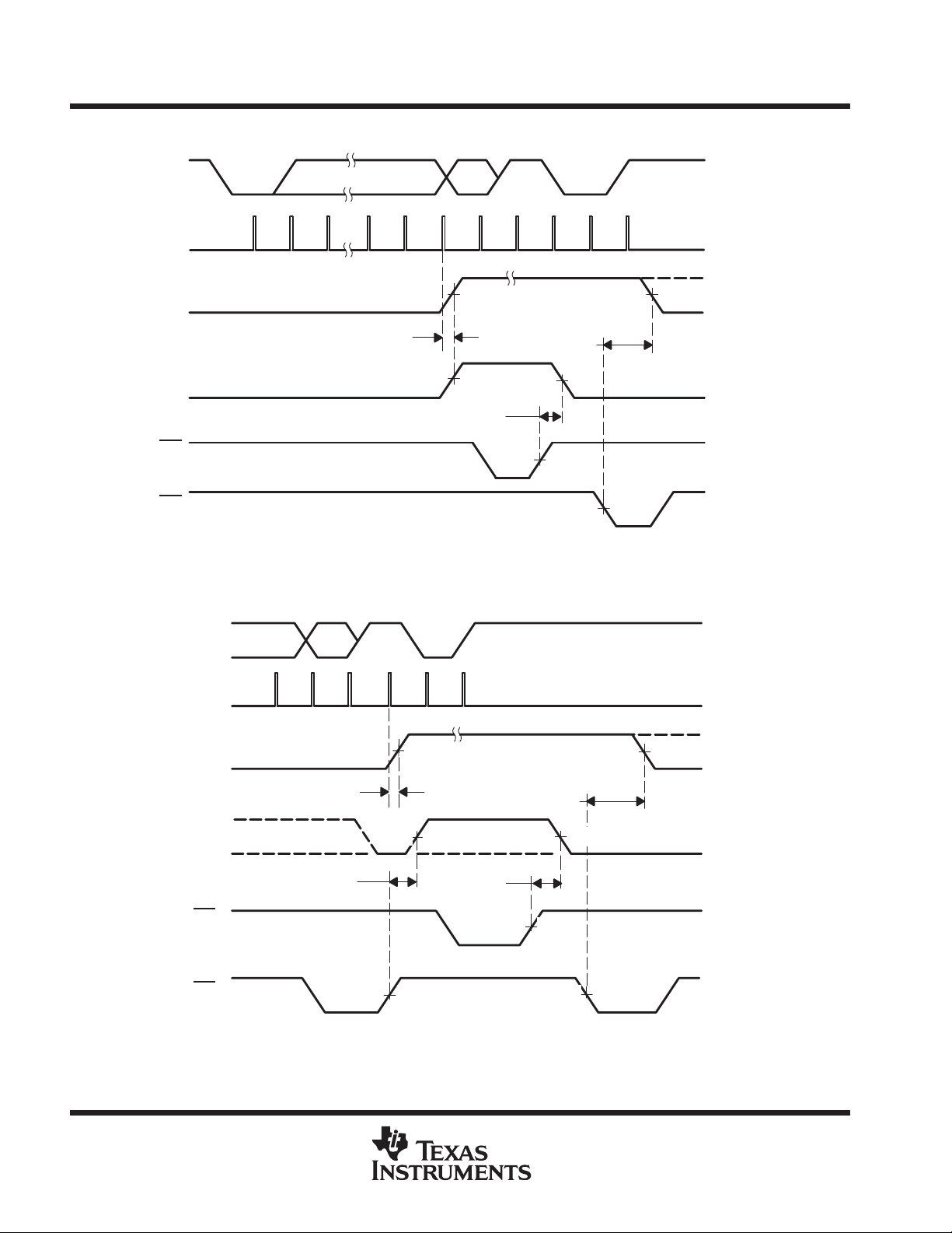
PARAMETER MEASUREMENT INFORMATION
IOW
RTSx, DTRx
CTSx, DSRx, DCDx
INTRPTx
(modem)
IOR
50% 50%
t
d23
50% 50%
50%
t
d16
50% 50%
t
d17
50%
RI
t
d23
50%
50%
t
d16
Figure 15. Modem-Control Timing
t
su2
CTSx
SOUTx
IOR (RBR)
SINx
RTSx
50% 50%
t
d18
50%
Figure 16. CTSx and SOUTx Auto Flow Control Timing (Start and Stop)
Midpoint of Stop Bit
t
d19
50%
t
50%
d20
50%
Figure 17. Auto-RTSx Timing for Receiver (RCV) Threshold of 1, 4, or 8
Midpoint of Stop Bit
POST OFFICE BOX 655303 • DALLAS, TEXAS 75265
19

TL16PIR552
DUAL UART WITH DUAL IrDA AND
1284 PARALLEL PORT
SLLS222A – DECEMBER 1995 – REVISED AUGUST 1996
PARAMETER MEASUREMENT INFORMATION
Midpoint of Data Bit 0
SINx
RTSx
IOR (RBR)
CLK
Sample Clock
(UART Internal)
RLCLK
(Internal)
BAUDOUT
(Internal)
SOUTx
(Internal)
15th Character 16th Character
t
d21
50%
Figure 18. Auto-RTS Timing for Receiver Threshold of 14 Bytes
t
d24
t
50%
d22
50%
SOUTx
(IR Mode)
IRSINx
SINx
t
d25
Figure 19. IR Signal Transfer
20
POST OFFICE BOX 655303 • DALLAS, TEXAS 75265

TL16PIR552
DUAL UART WITH DUAL IrDA AND
1284 PARALLEL PORT
SLLS222A – DECEMBER 1995 – REVISED AUGUST 1996
PARAMETER MEASUREMENT INFORMATION
ACK
PINTR (EPP)
(ECP)
FAULT
PINTR (ECP)
50%
t
d27
50%
50%
t
d26
50% 50%
Figure 20. Interrupt Timing Diagram
t
w4
POST OFFICE BOX 655303 • DALLAS, TEXAS 75265
21

TL16PIR552
DUAL UART WITH DUAL IrDA AND
1284 PARALLEL PORT
SLLS222A – DECEMBER 1995 – REVISED AUGUST 1996
PARAMETER MEASUREMENT INFORMATION
A0–A2
D7–0
IOW
IOCHRDY
STROBE
PD7–0
AUTOFD
t
d39
t
d36
50%
t
d34
50% 50%
t
d37
50% 50%
t
d28
t
d30
50% 50%
50% 50%
t
d35
t
d31
t
d29
t
h6
t
d38
22
SELECTIN
BUSY
t
d32
Figure 21. EPP Write Cycle
POST OFFICE BOX 655303 • DALLAS, TEXAS 75265
50%
t
d33
50% 50%50%

TL16PIR552
DUAL UART WITH DUAL IrDA AND
1284 PARALLEL PORT
SLLS222A – DECEMBER 1995 – REVISED AUGUST 1996
PRINCIPLES OF OPERATION
A0–A2
IOR
D7–0
IOCHRDY
STROBE
PD7–0
AUTOFD
50%
t
d42
50%
50%
t
d41
t
d44
t
d47
t
d40
50% 50%
t
d43
50%
t
h7
50%
t
d46
t
h8
SELECTIN
BUSY
t
d45
50%
Figure 22. EPP Read Cycle Timing
POST OFFICE BOX 655303 • DALLAS, TEXAS 75265
23

TL16PIR552
DUAL UART WITH DUAL IrDA AND
1284 PARALLEL PORT
SLLS222A – DECEMBER 1995 – REVISED AUGUST 1996
PRINCIPLES OF OPERATION
PD[7–0]
STROBE
BUSY
PD7–0
ACK
AUTOFD
50%
t
su3
t
d48
t
w5
50%50%
50% 50%
Figure 23. Parallel Port FIFO Timing
t
su4
50% 50%
t
d51
50%
t
d53
t
d54
50% 50%
Figure 24. ECP Parallel Port Reverse Timing
t
h9
50%
t
d49
t
d50
t
d52
24
AUTOFD
PD[7–0]
STROBE
BUSY
t
su5
t
d55
50% 50% 50%
t
d58
t
d59
t
d57
t
d60
t
Figure 25. ECP Parallel Port Forward Timing
POST OFFICE BOX 655303 • DALLAS, TEXAS 75265
d58
t
d56
t
h10
50%50%50%

TL16PIR552
DUAL UART WITH DUAL IrDA AND
1284 PARALLEL PORT
SLLS222A – DECEMBER 1995 – REVISED AUGUST 1996
PRINCIPLES OF OPERATION
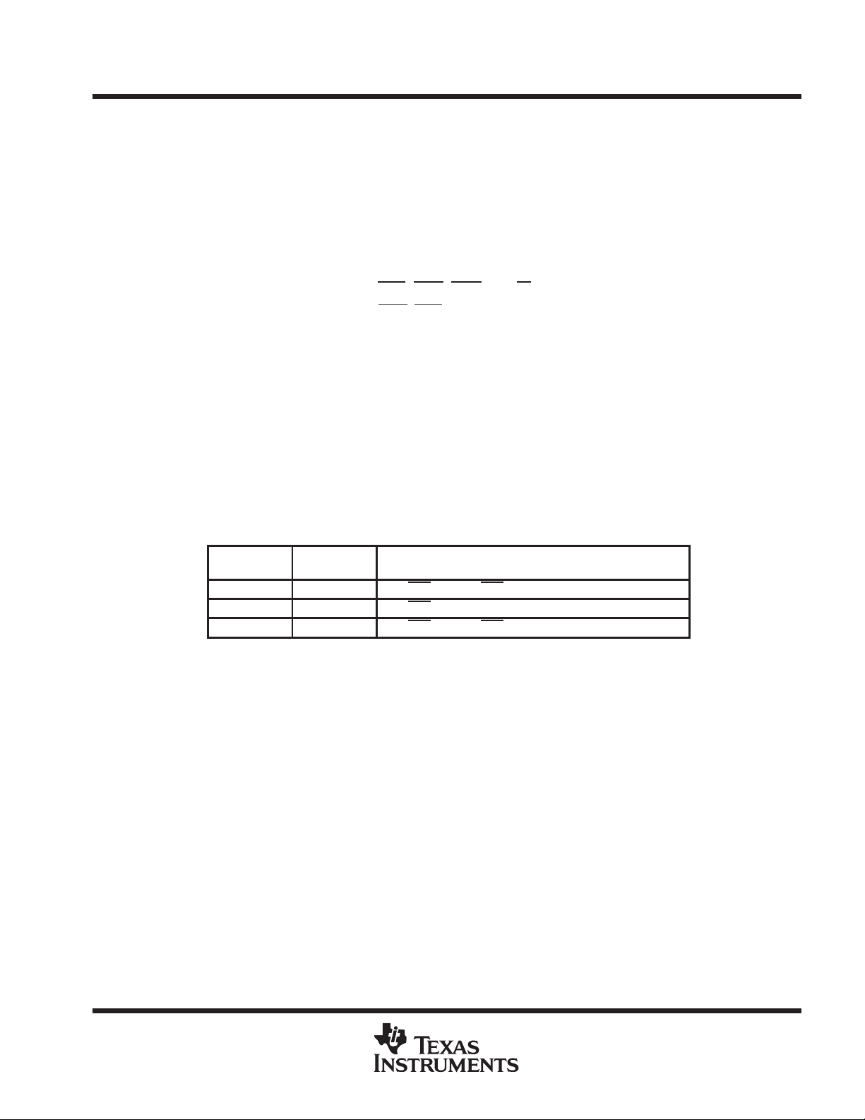
Table 1. Register Selection
†
DLAB
0 L L L Receiver buffer (read), transmitter holding register (write)
0 L L H Interrupt enable
X L H L Interrupt identification (read only)
X L H L FIFO control (write)
X L H H Line control
X H L L Modem control
X H L H Line status
X H H L Modem status
X H H H Scratch
1 L L L Divisor latch (LSB)
1 L L H Divisor latch (MSB)
†
The divisor-latch access bit (DLAB) is the most significant bit of the line-control register. The DLAB
signal is controlled by writing to this bit location (see Table 4).
A2 A1 A0 REGISTER
accessible registers
The system programmer, using the CPU, has access to and control over any of the UART registers that are
summarized in T able 2. These registers control UART operations, receive data, and transmit data. Descriptions
of these registers follow Table 3.
Table 2. UART Reset Functions
REGISTER/SIGNAL RESET CONTROL RESET STATE
Interrupt Enable Register Master Reset All bits low (0–3 forced and 4–7 permanent)
Interrupt Identification Register Master Reset
FIFO Control Register Master Reset All bits low
Line Control Register Master Reset All bits low
Modem Control Register Master Reset All bits low (6–7 permanent)
Line Status Register Master Reset Bits 5 and 6 are high; all other bits are low
Modem Status Register Master Reset Bits 0–3 are low; bits 4–7 are input signals
SOUT Master Reset High
INTRPT (receiver error flag) Read LSR/MR Low
INTRPT (received data available) Read RBR/MR Low
INTRPT (transmitter holding register empty) Read IR/Write THR/MR Low
INTRPT (modem-status changes) Read MSR/MR Low
RTS Master Reset High
DTR Master Reset High
Scratch Register Master Reset No effect
Divisor-Latch (LSB and MSB) Registers Master Reset No effect
Receiver Buffer Register Master Reset No effect
Transmitter Holding Register Master Reset No effect
RCVR FIFO MR/FCR1–FCR0/∆FCR0 All bits low
XMIT FIFO MR/FCR2–FCR0/∆FCR0 All bits low
Bit 0 is high, bits 1, 2, 3, 6, and 7 are low, and bits 4– 5 are
permanently low
POST OFFICE BOX 655303 • DALLAS, TEXAS 75265
25

TL16PIR552
DUAL UART WITH DUAL IrDA AND
1284 PARALLEL PORT
SLLS222A – DECEMBER 1995 – REVISED AUGUST 1996
PRINCIPLES OF OPERATION
Table 3. Summary of Accessible Registers
REGISTER ADDRESS
0DLAB=0 0 DLAB = 0 1 DLAB = 0 2 2 3 4 5 6 7 0DLAB =1 1 DLAB =1
Receiver
BIT
Buffer
NO.
Register
(Read
Only)
RBR THR IER IIR FCR LCR MCR LSR MSR SCR DLL DLM
0 Data Bit 0†Data Bit 0
1 Data Bit 1 Data Bit 1
2 Data Bit 2 Data Bit 2
3 Data Bit 3 Data Bit 3
4 Data Bit 4 Data Bit 4 0 0 Reserved
5 Data Bit 5 Data Bit 5 0 0 Reserved
6 Data Bit 6 Data Bit 6 0
7 Data Bit 7 Data Bit 7 0
†
Bit 0 is the least significant bit. It is the first bit serially transmitted or received.
NOTE 6: These bits are always 0 in the TL16C450 mode. When DLAB = 1, the six least significant bits of the scratch register contain the prescaler
value. IR logic is selected if the seventh bit of the scratch register is set to 1. Otherwise UART output is selected.
Transmitter
Holding
Register
(Write
Only)
Interrupt-
Enable
Register
Enable
Received-
Data-
Available
Interrupt
(ERBI)
Enable
Transmitter
Holding-
Register-
Empty
Interrupt
(ETBEI)
Enable
Receiver
Line-Status
Interrupt
(ELSI)
Enable
Modem-
Status
Interrupt
(EDSSI)
Interrupt-
Ident.
Register
(Read
Only)
0 if
Interrupt
Pending
Interrupt
ID
Bit 1
Interrupt
ID
Bit 2
Interrupt
ID
Bit 3
(see
Note 6)
FIFOs
Enabled
(see
Note 6)
FIFOs
Enabled
(see
Note 6)
FIFO
Control
Register
(Write
Only)
FIFO
Enable
Receiver
FIFO
Reset
Transmitter
FIFO
Reset
DMA
Mode
Select
Receiver
Trigger
(LSB)
Receiver
Trigger
(MSB)
Line-
Control
Register
Word-
Length
Select
Bit 0
(WLS0)
Word-
Length
Select
Bit 1
(WLS1)
Number
of
Stop Bits
(STB)
Parity
Enable
(PEN)
EvenParity
Select
(EPS)
Stick
Parity
Break
Control
Divisor-
Latch
Access
Bit
(DLAB)
Modem-
Control
Register
Data
Terminal
Ready
(DTR)
Request
to Send
(RTS)
OUT1
(an unused
internal
signal)
OUT2
Enable
external
interrupt
(INT0 or
INT1)
Loop
Autoflow
Control
Enable
(AFE)
0
0
Line-
Status
Register
Data
Ready
(DR)
Overrun
Error
(OE)
Parity
Error
(PE)
Framing
Error
(FE)
Break
Interrupt
(BI)
Transmitter
Holding
Register
(THRE)
Transmitter
Empty
(TEMT)
Error in
RCVR
FIFO
(see
Note 4)
Modem-
Status
Register
Delta
Clear
to Send
∆CTS)
(
Delta
Data-
Set
Ready
∆DSR)
(
Trailing-
Edge Ring
Indicator
(TERI)
Delta
DataCarrier
Detect
∆DCD)
(
Clear
to
Send
(CTS)
Data
Set
Ready
(DSR)
Ring
Indicator
(RI)
DataCarrier
Detect
(DCD)
Scratch
Register
Bit 0 Bit 0 Bit 8
Bit 1 Bit 1 Bit 9
Bit 2 Bit 2 Bit 10
Bit 3 Bit 3 Bit 11
Bit 4 Bit 4 Bit 12
Bit 5 Bit 5 Bit 13
Bit 6 Bit 6 Bit 14
Bit 7 Bit 7 Bit 15
Divisor
Latch
(LSB)
Divisor
Latch
(MSB)
26
POST OFFICE BOX 655303 • DALLAS, TEXAS 75265

TL16PIR552
DUAL UART WITH DUAL IrDA AND
1284 PARALLEL PORT
SLLS222A – DECEMBER 1995 – REVISED AUGUST 1996
PRINCIPLES OF OPERATION
receiver buffer register (RBR)
The UART receiver section of the TL16PIR552 consists of a receiver shift register (RSR) and a receiver buffer
register (RBR). The RBR is actually a 16-byte FIFO. Timing is supplied by the 16× receiver clock (RCLK).
Receiver-section control is a function of the UART line-control register.
The UART RSR receives serial data from SIN. The RSR then concatenates the data and moves it into the RBR
FIFO. In the TL16C450 mode, when a character is placed in the receiver buffer register and the
received-data-available interrupt is enabled (IER0 = 1), an interrupt is generated. This interrupt is cleared when
the data is read out of the receiver buffer register . In the FIFO mode, the interrupts are generated based on the
control setup in the FIFO-control register.
transmitter holding register (THR)
The UART transmitter section of the TL16PIR552 consists of a transmitter holding register (THR) and a
transmitter shift register (TSR). The THR is actually a 16-byte FIFO. Transmitter-section control is a function
of the UART line-control register.
The UART THR receives data off the internal data bus and when the shift register is idle, moves it into the TSR.
The TSR serializes the data and outputs it at SOUT. In the TL16C450 mode, if the THR is empty and the
transmitter holding-register-empty (THRE) interrupt is enabled (IER1 = 1), an interrupt is generated. This
interrupt is cleared when a character is loaded into the register. In the FIFO mode, the interrupts are generated
based on the control setup in the FIFO-control register.
interrupt enable register (IER)
The interrupt-enable register enables each of the five types of interrupts (refer to Table 4) and INTRPT in
response to an interrupt generation. The interrupt-enable register can also be used to disable the interrupt
system by setting bits 0 through 3 to logic 0. The contents of this register are summarized in Table 3 and are
described below.
Bit 0: When set to 1, bit 0 enables the received-data-available interrupt
Bit 1: When set to 1, bit 1 enables the transmitter holding-register-empty interrupt
Bit 2: When set to 1, bit 2 enables the receiver line-status interrupt
Bit 3: When set to 1, bit 3 enables the modem-status interrupt
Bits 4 through 7: These bits are not used (always set to 0)
interrupt identification register (IIR)
The UART has an on-chip interrupt generation and prioritization capability that permits a flexible interface with
most popular microprocessors.
The UART provides four prioritized levels of interrupts:
Priority 1 – Receiver line status (highest priority)
Priority 2 – Receiver data ready or receiver character timeout
Priority 3 – Transmitter holding-register empty
Priority 4 – Modem status (lowest priority)
POST OFFICE BOX 655303 • DALLAS, TEXAS 75265
27

TL16PIR552
DUAL UART WITH DUAL IrDA AND
1284 PARALLEL PORT
SLLS222A – DECEMBER 1995 – REVISED AUGUST 1996
PRINCIPLES OF OPERATION
interrupt identification register (IIR) (continued)
When an interrupt is generated, the interrupt identification register indicates that an interrupt is pending and
encodes the type of interrupt in its three least significant bits (bits 0, 1, and 2). The contents of this register are
summarized in Table 2 and described in Table 4. Detail on each bit is as follows:
Bit 0: Used either in a hardware-prioritized or polled-interrupt system. When this bit is a reset to 0, an
interrupt is pending; for a 1, no interrupt is pending.
Bits 1 and 2: The bits are used to identify the highest priority interrupt pending as indicated in Table 3
Bit 3: This bit is always 0 in the TL16C450 mode. In FIFO mode, this bit is set along with bit 2 to indicate that a
timeout interrupt is pending.
Bits 4 through 5: These bits are not used (always reset at 0).
Bits 6 and 7: These bits are always reset to 0 in the TL16C450 mode. They are set when bit 0 of the
FIFO-control register is equal to 1.
Table 4. Interrupt-Control Functions
INTERRUPT-
IDENTIFICATION
REGISTER
BIT 3 BIT 2 BIT 1 BIT 0
0 0 0 1 None None None None
0 1 1 0 1 Receiver line status
0 1 0 0 2 Received data available
1 1 0 0 2
0 0 1 0 3
0 0 0 0 4 Modem status
PRIORITY
LEVEL
INTERRUPT TYPE INTERRUPT SOURCE
Overrun error, parity error,
framing error, or break interrupt
Receiver data available in the
TL16C450 mode or trigger level
reached in the FIFO mode
No characters have been
Character time-out
indication
Transmitter holdingregister empty
removed from or input to the
receiver FIFO during the last
four character times, and there
is at least one character in it
during this time
Transmitter holding-register
empty
Clear to send, data-set ready,
ring indicator, or data-carrier
detect
INTERRUPT RESET
Read the line-status register
Read the receiver buffer
register
Read the receiver buffer
register
Read the interruptidentification register (if source
of interrupt) or writing into the
transmitter holding register
Read the modem-status
register
FIFO control register (FCR)
METHOD
The FIFO control register (FCR) is a write-only register at the same location as the IIR, which is a read-only
register. The FCR enables and clears the FIFOs, sets the receiver FIFO trigger level, and selects the type of
DMA signaling (see Table 5).
Bit 0: When set to 1, bit 0 enables the transmitter and receiver FIFOs. This bit must be set to 1 when other FCR
bits are written to or they are not programmed. Changing this bit clears the FIFOs.
28
POST OFFICE BOX 655303 • DALLAS, TEXAS 75265

TL16PIR552
DUAL UART WITH DUAL IrDA AND
1284 PARALLEL PORT
SLLS222A – DECEMBER 1995 – REVISED AUGUST 1996
PRINCIPLES OF OPERATION
FIFO control register (FCR) (continued)
Bit 1: When set to 1, bit 1 clears all bytes in the receiver FIFO and resets its counter logic to 0. The shift register
is not cleared. The one that is written to this bit position is self clearing.
Bit 2: When set to 1, bit 2 clears all bytes in the transmit FIFO and resets its counter to 0. The shift register is
not cleared. The one that is written to this bit position is self clearing.
Bit 3: When FCR0 is set to 1, setting FCR3 to a 1 causes RXRDY
and TXRDY to change from a 0 to a 1.
Bits 4 and 5: These bits are reserved for future use.
Bits 6 and 7: These bits are used to set the trigger level for the receiver FIFO interrupt.
Table 5. Bits 6 and 7 FCR
BIT 7 BIT 6
0 0 01
0 1 04
1 0 08
1 1 14
RECEIVER FIFO
TRIGGER LEVEL (BYTES)
line control register (LCR)
The system programmer controls the format of the asynchronous data-communication exchange through the
line-control register. In addition, the programmer is able to retrieve, inspect, and modify the contents of the
line-control register; this eliminates the need for separate storage of the line characteristics in system memory .
The contents of this register are summarized in Table 3 and described in the following paragraphs.
Bits 0 and 1: These two bits specify the number of bits in each transmitted or received serial character. These
bits are encoded as shown in Table 6.
Table 6. Bits 0 and 1 LCR
BIT 1 BIT 0 WORD LENGTH
0 0 5 bits
0 1 6 bits
1 0 7 bits
1 1 8 bits
POST OFFICE BOX 655303 • DALLAS, TEXAS 75265
29

TL16PIR552
DUAL UART WITH DUAL IrDA AND
1284 PARALLEL PORT
SLLS222A – DECEMBER 1995 – REVISED AUGUST 1996
PRINCIPLES OF OPERATION
line control register (LCR) (continued)
Bit 2: This bit specifies either one, one and one-half, or two stop bits in each transmitted character. When bit
2 is reset to 0, one stop bit is generated in the data. When bit 2 is set to 1, the number of stop bits generated
is dependent on the word length selected with bits 0 and 1. The receiver clocks only the first stop bit regardless
of the number of stop bits selected. The number of stop bits generated in relation to word length and bit 2 are
shown in Table 7.
Table 7. Bit 2 LCR
BIT 2
WORD LENGTH SELECTED
BY BITS 1 AND 2
0 Any word length 1
1 5 bits 11/2
1 6 bits 2
1 7 bits 2
1 8 bits 2
NUMBER OF STOP
BITS GENERATED
Bit 3: Parity enable bit. When bit 3 is set to 1, a parity bit is generated in transmitted data between the last
data-word bit and the first stop bit. In received data, when bit 3 is set to 1, parity is checked. When bit 3 is reset
to 0, no parity is generated or checked.
Bit 4: Even parity select bit. When parity is enabled by bit 3, a 1 in bit 4 produces even parity (an even number
of 1s in the data and parity bits) and a 0 in bit 4 produces odd parity (an odd number of 1s).
Bit 5: Stick parity bit. When bits 3, 4, and 5 are set to 1s, the parity bit is transmitted and checked as a 0. When
bits 3 and 5 are 1s and bit 4 is a 0, the parity bit is transmitted and checked as 1. When bit 5 is a 0, stick parity
is disabled.
Bit 6: Break control bit. Bit 6 is set to 1 to force a break condition; i.e., a condition where SOUT is forced to the
spacing (0) state. When bit 6 is reset to 0, the break condition is disabled and has no effect on the transmitter
logic; it only affects SOUT.
Bit 7: Divisor latch access bit (DLAB). Bit 7 must be set to 1 to access the divisor latches of the baud generator
during a read or write. Bit 7 must be reset to 0 during a read or write to access the receiver buffer , the transmitter
holding register, or the interrupt-enable register.
modem control register (MCR)
The modem control register is an 8-bit register that controls an interface with a modem, data set, or peripheral
device that is emulating a modem. The contents of this register are summarized in Table 3 and are described
in the following paragraphs.
Bit 0 (DTR) controls the DTR
Bit 1 (RTS) controls the RTS
Bit 2 Has no effect on operation.
Bit 3 When MCR3 is set, the external serial channel interrupt is enabled.
When any of bits 0-3 is set to 1, the associated output is forced low; a bit value of 0 forces the associated output
high.
30
output.
output.
POST OFFICE BOX 655303 • DALLAS, TEXAS 75265
TL16PIR552
DUAL UART WITH DUAL IrDA AND
1284 PARALLEL PORT
SLLS222A – DECEMBER 1995 – REVISED AUGUST 1996
PRINCIPLES OF OPERATION
modem control register (MCR) (continued)
Bit 4 (LOOP) provides a local loop-back feature for diagnostic testing of the UART. When LOOP is set to 1, the
following occurs:
• The transmitter SOUT is set high.
• The receiver SIN is disconnected.
• The output of the transmitter shift register is looped back into the receiver shift-register input.
• The four modem control inputs (CTS, DSR, DCD, and RI) are disconnected.
• The two modem control outputs (DTR, RTS) are internally connected to the four modem control inputs.
• The four modem control outputs are forced to the inactive (high) levels.
Bit 5 (AFE) is the autoflow control enable. When set high the autoflow control, as described in the detailed
description, is enabled.
In the diagnostic mode, data that is transmitted is immediately received. This allows the processor to verify the
transmit and receive data paths to the UART. The receiver and transmitter interrupts are fully operational. The
modem control interrupts are also operational, but the modem control interrupt sources are now the lower four
bits of the modem control register instead of the four modem control inputs. All interrupts are still controlled by
the interrupt enable register.
The UART flow can be configured by programming bits 1 and 5 of the MCR as shown in Table 8.
Table 8. UART Flow
MCR BIT 5
(AFE)
1 1 Auto-RTS and auto-CTS enabled (autoflow control enabled)
1 0 Auto-CTS only enabled
0 X Auto-RTS and auto-CTS disabled
MCR BIT 1
(RTS)
UART FLOW CONFIGURATION
line status register (LSR)
The line status register provides information to the CPU concerning the status of data transfers. The contents
of this register are described below and summarized in Table 3. The line status register is intended for read
operations only; writing to this register is not recommended outside of a factory testing environment. Bits 1–4
are the error conditions that produce a receiver line status interrupt.
Bit 0: Data ready (DR) indicator for the receiver. DR is set to 1 whenever a complete incoming character has
been received and transferred into the receiver buffer register or the FIFO. DR is reset to 0 by reading all of the
data in the receiver buffer register or the FIFO.
Bit 1: Overrun error (OE) indicator. When OE is set to 1, it indicates that before the character in the receiver buf fer
register was read, it was overwritten by the next character transferred into the register. OE is reset every time
the CPU reads the contents of the line status register. If the FIFO mode data continues to fill the FIFO beyond
the trigger level, an overrun error occurs only after the FIFO is full and the next character has been completely
received in the shift register. An overrun error is indicated to the CPU as soon as it happens. The character in
the shift register is overwritten, but it is not transferred to the FIFO.
POST OFFICE BOX 655303 • DALLAS, TEXAS 75265
31

TL16PIR552
DUAL UART WITH DUAL IrDA AND
1284 PARALLEL PORT
SLLS222A – DECEMBER 1995 – REVISED AUGUST 1996
PRINCIPLES OF OPERATION
line status register (LSR) (continued)
Bit 2: Parity error (PE) indicator. When PE is set to 1, it indicates that the parity of the received data character
does not match the parity selected in the line control register (bit 4). PE is reset every time the CPU reads the
contents of the line status register. In the FIFO mode, this error is associated with the particular character in the
FIFO to which it applies. This error is revealed to the CPU when its associated character is at the top of the FIFO.
Bit 3: Framing error (FE) indicator. When FE is set to 1, it indicates that the received character did not have a
valid (1) stop bit. FE is reset every time the CPU reads the contents of the line status register. In the FIFO mode,
this error is associated with the particular character in the FIFO to which it applies. This error is revealed to the
CPU when its associated character is at the top of the FIFO. The UART tries to resynchronize after a framing
error. To accomplish this, it is assumed that the framing error is due to the next start bit. The UART samples
this start bit twice and then accepts the input data.
Bit 4: Break interrupt (BI) indicator. When BI is set to 1, it indicates that the received data input was held in the
logic low state for longer than a full-word transmission time. A full-word transmission time is defined as the total
time to transmit the start, data, parity, and stop bits. BI is reset every time the CPU reads the contents of the
line status register. In the FIFO mode, this error is associated with the particular character in the FIFO to which
it applies. This error is revealed to the CPU when its associated character is at the top of the FIFO. When a break
occurs, only one 0 character is loaded into the FIFO. The next character transfer is enabled after SIN goes to
the marking state for at least two RCLK samples and then receives the next valid start bit.
Bit 5: Transmitter holding-register-empty (THRE) indicator. THRE is set to 1 when the transmitter holding
register is empty , indicating that the UART is ready to accept a new character . If the THRE interrupt is enabled
when THRE is set to 1, an interrupt is generated. THRE is set to 1 when the contents of the transmitter holding
register are transferred to the transmitter shift register. THRE is reset to 0 concurrent with the loading of the
transmitter holding register by the CPU. In the FIFO mode, THRE is set when the transmit FIFO is empty; it is
cleared when at least one byte is written to the transmit FIFO.
Bit 6: Transmitter empty (TEMT) indicator. TEMT bit is set to 1 when the transmitter holding register and the
transmitter shift register are both empty. When either the transmitter holding register or the transmitter shift
register contains a data character, TEMT is reset to 0. In the FIFO mode, TEMT is set to 1 when the transmitter
FIFO and shift register are both empty.
Bit 7: In the TL16PIR552, this bit is always reset to 0. In the TL16C450, this bit is always a 0. In the FIFO mode,
LSR7 is set to 1 when there is at least one parity, framing, or break error in the FIFO. It is cleared when the
microprocessor reads the LSR and there are no subsequent errors in the FIFO.
modem status register (MSR)
The modem status register is an 8-bit register that provides information about the current state of the control
lines from the modem, data set, or peripheral device to the CPU. Additionally, four bits of this register provide
change information; when a control input from the modem changes state, the appropriate bit is set to 1. All four
bits are reset to 0 when the CPU reads the modem status register. The contents of this register are summarized
in Table 3 and are described in the following paragraphs.
Bit 0: Change in clear to send (∆CTS) indicator. ∆CTS indicates that the CTS
the last time it was read by the CPU. When ∆CTS is set to 1 (autoflow control is not enabled and the modem
status interrupt is enabled), a modem status interrupt is generated. When autoflow control is enabled, no
interrupt is generated.
input has changed state since
Bit 1: Change in data set ready (∆DSR) indicator. ∆DSR indicates that the DSR
the last time it was read by the CPU. When ∆DSR is set to 1 and the modem status interrupt is enabled, a modem
status interrupt is generated.
32
POST OFFICE BOX 655303 • DALLAS, TEXAS 75265
input has changed state since

TL16PIR552
DUAL UART WITH DUAL IrDA AND
1284 PARALLEL PORT
SLLS222A – DECEMBER 1995 – REVISED AUGUST 1996
PRINCIPLES OF OPERATION
modem status register (MSR) (continued)
Bit 2: Trailing edge-of-the-ring indicator (TERI) detector . TERI indicates that the RI input to the chip has changed
from a low to a high level. When TERI is set to 1 and the modem status interrupt is enabled, a modem status
interrupt is generated.
Bit 3: Change in data carrier detect (∆ DCD) indicator. ∆ DCD indicates that the DCD
changed state since the last time it was read by the CPU. When ∆DCD is set to 1 and the modem status interrupt
is enabled, a modem status interrupt is generated.
Bit 4: Complement of the clear to send (CTS
[MCR4] = 1), this bit is equal to the modem control register bit 1 (RTS).
Bit 5: Complement of the data set ready (DSR
[MCR4] = 1), this bit is equal to the modem control register bit 0 (DTR).
Bit 6: Complement of the ring indicator (R
[MCR4] = 1), this bit is equal to the modem control register bit 2 (OUT1).
Bit 7: Complement of the data carrier detect (DCD
[MCR4] = 1), this bit is equal to the modem control register bit 3 (OUT2).
) input. When the UART is in the diagnostic test mode (LOOP
) input. When the UART is in the diagnostic test mode (LOOP
I) input. When the UART is in the diagnostic test mode (LOOP
) input. When the UART is in the diagnostic test mode (LOOP
input to the chip has
scratch register (SCR)
The scratch register is an 8-bit register that is intended for programmer use as a scratchpad in the sense that
it temporarily holds the programmer data without affecting any other UART operation.
prescaler
When DLAB = 1, the six least significant bits of the scratch register contain the prescaler value. IR logic is
selected when the seventh bit is set to 1. Otherwise UART output is selected. After reset, UART0 is in IR mode
and UART1 is in UART mode.
prescaler descriptions
The clock prescaler allows for the divisor from 0 to 31.5 in 0.5 increments (scr(0) is the half-bit divider). The
divisor value is loaded from scratch register with DLAB = 1. The output of the divisor feeds the UART clock. A
programmed divisor between 2 and 7.5 drives the UART clock low for one XIN clock cycle for integer divisor
and 1.5 XIN clock cycles for integer-plus a half clock divisor. A programmed divisor of eight or greater drives
the UART clock low for four XIN clock cycles for integer divisors and 4.5 XIN clock cycles for integer-plus-a-half
divisor. Based on the above parameters, the acceptable XIN/divisor combinations can be derived. The precision
of the programmable clock generator for integer-plus-a-half divisor depends on the closeness to a 50% duty
cycle for the XIN input clock.
Example: When the oscillator frequency is 22 Mhz (see Table 9).
Table 9. Typical Prescaler Example
XIN PRESCALER DIVISOR UART CLOCK UART DIVISOR BAUD RATE
22.118 Mhz 5.5 4 Mhz 8 31.25k
22.118 Mhz 3 7.33 Mhz 1 458K
POST OFFICE BOX 655303 • DALLAS, TEXAS 75265
33

TL16PIR552
DUAL UART WITH DUAL IrDA AND
1284 PARALLEL PORT
SLLS222A – DECEMBER 1995 – REVISED AUGUST 1996
PRINCIPLES OF OPERATION
prescaler descriptions: (continued)
When DLAB = 1, the six least significant bits of the scratch register contain the prescaler value.
Table 10. SCR (0–5) Values
SCR(0-5) Value (Hex) Result
0 (0) No Clock (high)
0.5 (1) divide-by-1
1 (2) divide-by-1
1.5 (3) divide-by-1
2 (4) to 31.5 (3F) divide by 2 to 31.5
programmable baud generator
The UART contains a programmable baud generator that takes a clock input in the range between dc and 16
MHz and divides it by a divisor in the range between 1 and 2
is 16 times (16×) the baud rate. The formula for the divisor is:
divisor = XIN frequency input ÷ (desired baud rate × 16)
Two 8-bit registers, called divisor latches, store the divisor in a 16-bit binary format. These divisor latches must
be loaded during initialization of the UART in order to ensure desired operation of the baud generator. When
either of the divisor latches is loaded, a 16-bit baud counter is also loaded to prevent long counts on initial load.
T ables 5 and 6 illustrate the use of the baud generator with crystal frequencies of 1.8432 MHz and 3.072 MHz,
respectively. For baud rates of 38.4 kbits/s and below, the error obtained is very small. The accuracy of the
selected baud rate is dependent on the selected crystal frequency (refer to Figure 16 for examples of typical
clock circuits).
16
–1. The output frequency of the baud generator
FIFO interrupt mode operation
When the receiver FIFO and receiver interrupts are enabled (FCR0 = 1, IER0 = 1, IER2 = 1), a receiver interrupt
occurs as follows:
• The received-data-available interrupt issued to the microprocessor when the FIFO has reached its
programmed trigger level. It is cleared when the FIFO drops below its programmed trigger level.
• The IIR receive-data-available indication also occurs when the FIFO-trigger level is reached, and like
the interrupt, it is cleared when the FIFO drops below the trigger level.
• The receiver line-status interrupt (IIR = 06) has higher priority than the received-data-available (IIR =
04) interrupt.
• The data ready bit (LSR0) is set when a character is transferred from the shift register to the receiver
FIFO. It is reset when the FIFO is empty.
34
POST OFFICE BOX 655303 • DALLAS, TEXAS 75265

PRINCIPLES OF OPERATION
FIFO interrupt mode operation (continued)
When the receiver FIFO and receiver interrupts are enabled:
• FIFO timeout interrupt occurs when the following conditions exist:
– At least one character is in the FIFO.
– The most recent serial character was received more than four continuous character times ago (if
two stop bits are programmed, the second one is included in this time delay).
– The most recent microprocessor read of the FIFO occurred more than four continuous character
times ago. This causes a maximum character received to interrupt an issued delay of 160 ms at
300 baud with a 12-bit character.
• Character times are calculated by using the RCLK input for a clock signal that makes the delay
proportional to the baud rate.
• When a timeout interrupt has occurred, it is cleared and the timer is reset when the microprocessor
reads one character from the receiver FIFO.
• When a timeout interrupt has not occurred, the timeout timer is reset after a new character is received or
after the microprocessor reads the receiver FIFO.
TL16PIR552
DUAL UART WITH DUAL IrDA AND
1284 PARALLEL PORT
SLLS222A – DECEMBER 1995 – REVISED AUGUST 1996
When the transmitter FIFO and THRE interrupt are enabled (FCR0 = 1, IER1 = 1), transmit interrupts occur as
follows:
• The occurrence of transmitter holding-register-empty interrupt (IIR(3–0) = 2) is delayed one character
time minus the last stop bit time when there have not been at least two bytes in the transmitter FIFO at
the same time since the last time the transmitter FIFO was empty . It is cleared (IIR(3–0) = 1) as soon as
the transmitter holding register is written to (1 to 16 characters may be written to the transmit FIFO while
servicing this interrupt) or the IIR is read. The first transmitter interrupt after changing FCR is immediate
if it is enabled.
• The transmitter empty indicator (LSR6 (TEMT) = 1) is delayed one character time when there has not
been at least two bytes in the transmitter FIFO at the same time since the last time that TEMT = 1. TEMT
is set after the stop-bit has been completely shifted out (finishes one complete bit time or 16 BAUDOUT
cycles).
• The transmitter FIFO empty indicator (LSR5 (THRE) = 1) works the normal way in this mode and is not
delayed.
Character timeout and receiver FIFO trigger-level interrupts have the same priority as the current
received-data-available interrupt.
POST OFFICE BOX 655303 • DALLAS, TEXAS 75265
35

TL16PIR552
DUAL UART WITH DUAL IrDA AND
1284 PARALLEL PORT
SLLS222A – DECEMBER 1995 – REVISED AUGUST 1996
PRINCIPLES OF OPERATION
FIFO polled mode operation
With FCR0 = 1 (transmitter and receiver FIFOs enabled), resetting IER0, IER1, IER2, IER3, or all four to 0 puts
the UART in the FIFO polled mode of operation. Since the receiver and transmitter are controlled separately,
either one or both can be in the polled mode of operation.
In this mode, the user program checks receiver and transmitter status using the LSR. As stated previously:
• LSR0 is set as long as there is one byte in the receiver FIFO.
• LSR (1–4) specify which error(s) have occurred. Character error status is handled the same way as
when in the interrupt mode; the IIR is not affected since IER2 = 0.
• LSR5 indicates when the transmitter holding register is empty.
• LSR6 indicates that both the transmitter holding register and transmitter shift register are empty.
• LSR7 indicates whether there are any errors in the receiver FIFO.
There is no trigger level reached or time-out condition indicated in the FIFO-polled mode. However, the receiver
and transmitter FIFOs are still fully capable of holding characters (See Table 11 and 12).
Table 11. Baud Rates Using a 1.8432-MHz Crystal
DESIRED
BAUD RATE
50 2304
75 1536
110 1047 0.026
134.5 857 0.058
150 768
300 384
600 192
1200 96
1800 64
2000 58 0.69
2400 48
3600 32
4800 24
7200 16
9600 12
19200 6
38400 3
56000 2 2.86
DIVISOR USED
TO GENERATE
16× CLOCK
PERCENT OF ERROR
DIFFERENCE BETWEEN
DESIRED AND ACTUAL
BAUD RATES
36
POST OFFICE BOX 655303 • DALLAS, TEXAS 75265

TL16PIR552
DUAL UART WITH DUAL IrDA AND
1284 PARALLEL PORT
SLLS222A – DECEMBER 1995 – REVISED AUGUST 1996
PRINCIPLES OF OPERATION
Table 12. Baud Rates Using a 3.072-MHz Crystal
DESIRED
BAUD RATE
50 3840
75 2560
110 1745 0.026
134.5 1428 0.034
150 1280
300 640
600 320
1200 160
1800 107 0.312
2000 96
2400 80
3600 53 0.628
4800 40
7200 27 1.23
9600 20
19200 10
38400 5
DIVISOR USED
TO GENERATE
16× CLOCK
PERCENT OF ERROR
DIFFERENCE BETWEEN
DESIRED AND ACTUAL
BAUD RATES
External
Clock
Optional
Clock
Output
Driver
Optional
Driver
V
CC
XIN
C1
Crystal
R
P
XOUT
CRYSTAL
3.072 MHz 1 MΩ 1.5 kΩ 10–30 pF 40–60 pF
1.8432 MHz 1 MΩ 1.5 kΩ 10–30 pF 40–60 pF
Oscillator Clock
to Baud-Generator
Logic
C2
TYPICAL CRYSTAL OSCILLATOR NETWORK
R
P
RX2 C1 C2
RX2
XOUT
Figure 26. Typical Clock Circuits
XIN
V
CC
Oscillator Clock
to Baud-Generator
Logic
POST OFFICE BOX 655303 • DALLAS, TEXAS 75265
37

TL16PIR552
DUAL UART WITH DUAL IrDA AND
1284 PARALLEL PORT
SLLS222A – DECEMBER 1995 – REVISED AUGUST 1996
PRINCIPLES OF OPERATION
IR encoder and decoder
The IR encoder and decoder circuitry work with the UART to change the serial bit stream into a series of pulses
and back again. For every zero bit in the serial stream, a pulse is sent at the middle of the bit with a duration
of 3/16 of a bit time. If a one or series of ones is sent, the encode does not send a pulse. The decoding process
consists of receiving a pulse and sending a stretched version of the pulse to the UART. The stretched version
must be at least three-fourths of a bit time to be correctly decoded by most UARTs. Because the serial stream
can occur at any baud rate, some means of changing the encoding and decoding baud rate is needed. The
easiest way to accomplish this is to clock the encoder and decoder circuits with the UART baud rate 16x clock.
A block diagram of a design is shown in Figure 27.
TX
IR Transmit
Formatter
IRTX
UART
UART CLK
RX
IR Receive
Decoder
IRRX
Figure 27. Conventional UART Connection to the External IR Encoder and Decoder
The encoder uses a 4-bit synchronous counter to transmit the pulses. It uses a delay of one-half of a bit time
to insure that a true zero bit has been sent. It sends a pulse for three UART clocks in the middle of the zero bit.
When two zeros are sent in a row, the counter simply overruns at the beginning of the next zero bit and starts
the process over. When a 1 is sent, the counter is reset.
The decoder also uses a 4-bit synchronous counter including a synchronous reset. The rising edge of an
incoming pulse sets the input flip-flop. This causes the counter to begin counting and a zero to be sent out at
the RX signal output. When the counter gets to 16, the input flip-flop is reset to wait for another input pulse. If
another pulse occurs before the counter expires, the counter is synchronously reset and the RX signal output
remains 0. When the counter expires, the RX signal output returns to 1, and the circuit waits for another input
pulse.
38
POST OFFICE BOX 655303 • DALLAS, TEXAS 75265

TL16PIR552
DUAL UART WITH DUAL IrDA AND
1284 PARALLEL PORT
SLLS222A – DECEMBER 1995 – REVISED AUGUST 1996
PRINCIPLES OF OPERATION
IR encoder and decoder (continued)
IR mode can be chosen through the use of SLR(6) with DLAB = 1. With DLAB = 1 and if SCR(6) = 1, IR mode
is selected. Built in multiplexers are used to choose the correct signal to input to the UART. Refer to Figure 28
for more detail.
From UART
SOUT
SOUT
IR
Encoder
t
A
t
B
To ACE
IR_TX
SCR 6
SIN
Figure 28. TL16PIR552 Mode Select
SOUT TX
BDOUT CLK
UART
SIN RX
RCLK CLK
MR
IR
Encoder
Transmitter
IR
Decoder
Receiver
0
SOUT
M
U
X
1
0
M
U
X
1
To 232 Port
or IR Module
SIN
From 232 Port
Decoder
IR_TX
IR_RX
IR
IRSIN
From IR
Module
Figure 29. TL16PIR552 IR Encoder/Decoder
For encoding, the IR_TX is selected when SCR6 is set to 1. This sends IR_TX on the device SOUT terminal.
This signal can be used as an input to any IR transceiver (see Figure 29).
For decoding, the IRSIN from the device (this can be connected to any IR transceiver) goes through the IR
decode block and then it is the input to the UART (see Figure 29).
POST OFFICE BOX 655303 • DALLAS, TEXAS 75265
39

TL16PIR552
DUAL UART WITH DUAL IrDA AND
1284 PARALLEL PORT
SLLS222A – DECEMBER 1995 – REVISED AUGUST 1996
PRINCIPLES OF OPERATION
parallel port (see Table 13)
The parallel port is essentially an extended capabilities port with an additional enhanced parallel port mode, and
includes the following features:
• Compatible with standard Centronics parallel interface
• Support for ECP and EPP
• Data path FIFO buffer
• Direct Memory Access (DMA) transfer
• Decompression of run length encoded data in ECP reverse mode
The parallel port is an extended capabilities parallel (ECP) port with additional enhanced parallel port (EPP)
protocol support. Modes 000 and 001 are compatible with Centronics and bidirectional Centronics ports, and
mode 100 is defined to be EPP mode. Thus, together with the ECP protocol modes, the parallel port supports
three distinct transfer protocols which all share the standard parallel port signals.
The parallel port consists of an 8-bit host interface (including DMA support) which is connected to the fast-A T
bus, a sequencer containing state-machines for the three different protocols, a 16-byte FIFO data path and a
parallel interface.
transfer protocols
There are three parallel port transfer protocols in the TL16PIR552. Descriptions of these protocols follow and
specifications with terminal numbers follow in Table 13.
standard Centronics protocol
In the standard Centronics modes, the parallel port is compatible with the Centronics unidirectional or
bidirectional parallel port. It consists of a single-byte data port which writes and reads data to/from the port data
lines and registers to control and reflect the status of the parallel port signals. Signaling protocol is handled by
software, which must assert control strobes and poll for acknowledgement itself.
enhanced parallel port (EPP protocol)
In enhanced parallel port mode, SELECTIN
address strobe and data strobe, respectively, while STROBE
addresses are defined for data and address accesses and when these locations are used, handshaking is
performed automatically by hardware.
extended capabilities port (ECP) protocol
The enhanced capability port specification is an enhancement to the IEEE 1284 standard; it defines new transfer
protocols and timing which offer a reverse channel as fast as the forward channel. Software overhead is reduced
by direct memory access (DMA) support, data buffering, and automatic strobe generation. ECP defines
separate I/O locations for address and data accesses.
and AUTOFD are automatically generated and are redefined to be
indicates a write or a read cycle. Additional I/O
40
POST OFFICE BOX 655303 • DALLAS, TEXAS 75265

TL16PIR552
DUAL UART WITH DUAL IrDA AND
1284 PARALLEL PORT
SLLS222A – DECEMBER 1995 – REVISED AUGUST 1996
PRINCIPLES OF OPERATION
Table 13. Parallel Port Connector Specifications
Terminal
Number
56 STROBE WRITE HOSTCLK
52-49, 44-47 PD0–7 PD0–7 PD0–7
27 ACK INTR PERIPHCLK
26 BUSY WAIT PERIPHACK
23 PERROR USER DEFINED MPERIPHREQUEST
24 SELECT USER DEFINED USER DEFINED
57 AUTOFD DSTRB HOSTACK
25 FAULT USER DEFINED PERIPHREQUEST
54 INIT INIT REVERSEREQUEST
55 SELECTIN ASTRB SELECTIN (1,3)
NOTE 7: For the cable interconnection required for ECP support and the slave connector terminal
numbers, refer to the
7, 1993. This document is available from Microsoft.
Standard EPP ECP
Extended Capabilities Port Protocol and ISA Standard
, Rev. 1.09, Jan.
parallel port modes of operation (see Table 14)
The seven parallel port operating modes are selected by bits 7-15 of the extended control register.
1. Standard Centronics mode (000)
This is the default mode in which the parallel port behavior is compatible with the Centronics standard port. The
FIFO is reset and the direction bit in the device control register has no effect.
2. Bidirectional Centronics standard mode (001)
This is the same as mode 000 except that setting the direction bit puts the data line in a high-impedance state
and reading the data register returns the value on the data lines.
3. Parallel port FIFO mode (010)
In this mode bytes written or DMA transferred to the FIFO are transmitted automatically using the Centronics
standard protocol. Only the forward direction is useful.
4. ECP mode (011)
In the forward direction (direction = 0) data written to the ECPDFIFO and bytes written to ECPAFIFO addresses
are placed in a single FIFO and transmitted automatically using ECP protocol. In the reverse direction
(direction = 1) data bytes are transferred from the ECP parallel port and placed in the ECPDFIFO.
5. Enhanced parallel port mode (100)
In this mode, EPP read, write, or address/data cycles can be executed or, if no EPP cycle is pending, compatible
Centronics standard access can be made (as in mode 001). Note that the software must ensure that the
direction = 0 before attempting to perform an EPP write cycle.
6. FIFO test mode (110)
In this mode the FIFO can be written and read or DMA transferred in any direction, but no data will be transmitted
on the parallel port. The FIFO does not stop accepting or sending data when full or empty conditions occur; FIFO
read and write address counters will wrap.
7. Configuration mode (111)
In this mode the CONFGA and CONFGB registers are accessible.
Microsoft is a registered trademark of Microsoft Corporation.
POST OFFICE BOX 655303 • DALLAS, TEXAS 75265
41

TL16PIR552
DUAL UART WITH DUAL IrDA AND
1284 PARALLEL PORT
SLLS222A – DECEMBER 1995 – REVISED AUGUST 1996
PRINCIPLES OF OPERATION
T able 14. Mode Summary
MODE DESCRIPTION
000 Centronics (default) mode, forward direction only
001 Bidirectional Centronics mode
010 Parallel port data FIFO mode
011 ECP Parallel port mode
100 EPP mode
110 Test mode
111 Configuration mode
mode switching
Mode switching is only allowed into and out of the modes 000 and 001. All 1284 negotiation takes place in these
two modes. Setting the mode to 011 (ECP Parallel Port mode) causes the hardware to initiate data transfer.
Switching out of modes 011 and 010 in the middle of a transfer or when data remains in the FIFO causes the
transfer to be aborted and the data to be lost.
data compression
The TL16PIR552 supports run length encoded (RLE) decompression in hardware and can transfer compressed
data to a peripheral. Run length encoded (RLE) compression in hardware is not supported. To transfer
compressed data in ECP mode, the compression count is written to the ECP AFIFO and a data byte is written
to the ECPDFIFO.
Compression is accomplished by counting identical bytes and transmitting an RLE byte that indicates how many
times the next byte is to be repeated. Decompression simply intercepts the RLE byte and repeats the following
byte the specified number of times. When a run-length count is received from a peripheral, the subsequent data
byte is replicated that specified number of times. A run-length count of zero specifies that only one byte of data
is represented by the next data byte. A run-length count of 127 indicates that the next byte should be expanded
to 128 bytes. To prevent data expansion, however, run-length counts of zero should be avoided.
The RLE command byte is loaded to the FIFO. Then the logic offloads this command to the decompression
counter to generate the correct number of decompressed data available. The logic asserts PDRQ only when
there are data bytes in the FIFO. Although the command byte is loaded to the FIFO, the PDRQ is not asserted.
42
POST OFFICE BOX 655303 • DALLAS, TEXAS 75265

DUAL UART WITH DUAL IrDA AND
1284 PARALLEL PORT
SLLS222A – DECEMBER 1995 – REVISED AUGUST 1996
PRINCIPLES OF OPERATION
register definitions
Table 15 is a summary of the parallel port internal registers, assuming 378h is the base address.
Table 15. Parallel port internal register
Chip
Select
PPCS 000 Std/Bidi (000–001) R/W DATA Data port
ECPCS 000 ECP (011) R/W ECPDFIFO ECP data FIFO
A2–A0 Mode Access Name Function
000 ECP (011) W ECPAFIFO ECP address FIFO
001 All R DSR Status register
010 All R/W DCR Control register
011 EPP (100) R/W EPPADDR EPP address port
100–1 11 EPP (100) R/W EPPDA TA EPP data Port
000 CFIFO (010) R/W PP DATA
FIFO
000 TFIFO (110) R/W TEST FIFO
000 Config (111) R CNFGA Configuration register A
001 Config (111) R CNFGB Configuration register B
010 All R/W ECR Extended control register
Parallel port data FIFO
TL16PIR552
data register (DATA)
This is the standard parallel port data register. In standard mode, writing to this register drives data onto the
parallel port data lines. In all other modes, the drivers may be put into a high-impedance state by setting the
direction bit in the DCR. Reads to this register return the value of the data lines.
ECP address FIFO register (ECPAFIFO)
A data byte written to this register is placed in the FIFO and tagged as an ECP address. T able 16 is a summary
of the device status register bits and their descriptions. T able 17 is a summary of the device control register bits
and their descriptions.
Table 16. Device status register (DSR)
Bit Default Name Description
7 Default BUSY Bit 7 corresponds to the inverse of a BUSY input
6 – ACK Bit 6 corresponds to the ACK input
5 – PE Bit 5 corresponds to the PERROR input
4 – SLCT Bit 4 corresponds to the SELECT input
3 – ERR Bit 3 corresponds to the FAULT input
2 – PRINT Print interrupt. Bit 2 is reset to 0 by the rising transition of ACK and set to 1 by a read
1 0 – Bit 1 is reserved
0 0 TIMEOUT When enabled in EPP mode, bit 0 is set to 1 when 10-µs timeout occurs. Bit 0 is cleared
operation of this register.
by any write operation to the DSR register.
POST OFFICE BOX 655303 • DALLAS, TEXAS 75265
43

TL16PIR552
DUAL UART WITH DUAL IrDA AND
1284 PARALLEL PORT
SLLS222A – DECEMBER 1995 – REVISED AUGUST 1996
PRINCIPLES OF OPERATION
Table 17. Device Control Register (DCR)
Bit Default Name Description
7 1 – This bit is reserved
6 1 – This bit is reserved
5 0 DIR In standard and CFIFO modes this bit has no effect; in all other modes, when set to 1
4 0 INT2EN When high, this bit enables interrupts to access the host (on the rising edge of ACK).
3 0 SLIN 1: SELECT output active;
2 0 INIT 0: INIT output active;
1 0 AFD 1: AUTOFD output active;
0 0 STB 1: STROBE output active;
this bit put the parallel port data lines into a high-impedance state, 0 = forward, 1 = reverse.
0: SELECT
1: INIT
0 AUTOFD
0: STROBE
output inactive.
output inactive.
output inactive.
output inactive.
EPP address register (EPPADDR)
This is the EPP address strobe register. In EPP mode, an address strobe is automatically generated when data
is read from or written to this register. This register is only available in EPP mode.
EPP data register (EPPDA TA)
This is the EPP data strobe register. In EPP mode, a data strobe is automatically generated when data is read
or written to this register. This register is only available in EPP mode.
ECP Data FIFO register (ECPDFIFO)
A data byte wirtten or DMA transferred to this register is placed in the FIFO and tagged as ECP data in forward
direction. Data bytes from peripherals are read under an automatic hardware handshake from ECP into this
FIFO when the direction bit is set to 1. Table 18 is a description of the bits in the ECP configuration, register A.
Table 19 is a description of the bits in the ECP configuration, register B. Table 20 is a description of the bits in
the extended control register.
Table 18. ECP Configuration Register A (CNFGA)
Bit Name Description
7–4 IMPLD Bits 7–4 are used for the implementation ID number. Always read as 0001, 8-bit implementation (PWord =
3–0 – These bits are reserved; read as 1s
1 byte)
Table 19. Configuration Register B (CNFGB)
Bit Name Description
7 COMPRESS Bit 7 always read as a 0: Compression is not supported
6 INTRVALUE Bit 6 returns value on IRQ line to determine possible conflicts
5–3 INTRLINE Bits 5–3 are always read as 001: IRQ7 selected
2–0 DMACHNL Bits 2–0 are always read as 011: DMA channel 3 selected
44
POST OFFICE BOX 655303 • DALLAS, TEXAS 75265

DUAL UART WITH DUAL IrDA AND
1284 PARALLEL PORT
SLLS222A – DECEMBER 1995 – REVISED AUGUST 1996
PRINCIPLES OF OPERATION
Table 20. Extended Control Register (ECR)
Bit Access Name Description
7–5 R/W MODE Bits 7–5 have the following selected modes of operation:
000: Standard Parallel Port mode (forward direction only)
001: Bidirectional Parallel Port mode
010: Parallel Port FIFO mode (forward direction only)
011: ECP Parallel Port mode
100: EPP mode
101: reserved
110: FIFO test mode
111: Configuration mode
4 R/W ERRINTREN In ECP mode, when bit 4 is set to 0, an interrupt on the falling edge of FAUL T is en-
abled. A 1 disables the interrupt.
3 R/W DMAEN When bit 3 is reset to 0, DMA is disabled. A bit setting of 1 enables the DMA. The
DMA starts when SERVICEINTR is reset to 0.
2 R/W SERVICEINTR When bit 2 is set to 1, DMA and all service interrupts are disabled.
1 R FULL When bit 1 is set to 1, the FIFO is full.
0 R EMPTY When bit 0 is set to 1, the FIFO is empty.
TL16PIR552
CFIFO parallel port data FIFO
Bytes written or DMA transferred from the system to this FIFO are transmitted by a hardware handshake to the
peripheral using the standard parallel port protocol. This mode is only defined for the forward direction.
TFIFO test mode
Data bytes can be read, written, or DMA transferred to or from the system to this FIFO in any direction. Data
in the TFIFO register is not transmitted to the parallel port lines using a hardware protocol handshake. However,
data in the TFIFO may be displayed on the parallel port data lines. The TFIFO does not stall when overwritten
or underrun. Data is simply rewritten or overrun. The FULL and EMPTY bits must always keep track of the
correct FIFO state. The TFIFO transfers data at the maximum ISA rate so that software may generate
performance metrics.
The WRITEINTR threshold can be determined by starting with a full TFIFO, and emptying it one byte at a time
until the SERVICEINTR bit is set. This may generate a spurious interrupt, but indicates that the threshold has
been reached. Likewise, READINTR threshold can be determined by setting the direction bit to 1, and filling the
empty TFIFO a PWord at a time until SERVICEINTR bit is set. Data bytes are always read from the head of
TFIFO regardless of the value of the direction bit. For example, when a 0x4433, 0x221 1, or a 0x00f f is written
to the FIFO, then reading the TFIFO returns a 0x4433, a 0x2211,or a 0x0ff in the same order in which it was
written. The FIFO size and interrupt threshold can be determined by writing PWords and checking the FULL
and SERVICEINTR bits.
POST OFFICE BOX 655303 • DALLAS, TEXAS 75265
45

TL16PIR552
DUAL UART WITH DUAL IrDA AND
1284 PARALLEL PORT
SLLS222A – DECEMBER 1995 – REVISED AUGUST 1996
PRINCIPLES OF OPERATION
description of printer operation
ECP: command/data
The ECP mode supports two advanced features to improve the effectiveness of the protocol for some
applications. The features are implemented by allowing the transfer of normal 8-bit data or 8-bit commands.
When in the forward direction, normal data is transferred when AUTOFD
transferred when AUTOFD
The most significant bit of the command indicates whether it is a run-length count (for compression) or a channel
address.
When in the reverse direction, normal data is transferred when BUSY is high and an 8-bit command is
transferred when BUSY is low. The most significant bit of the command is always zero. Reverse channel
addresses are seldom used and may not be supported in hardware.
run length encoded data compression
The parallel port supports decompression of run length encoded (RLE) data in ECP DMA mode (01 1) reverse
direction only . During reverse direction transfers, the peripheral indicates a command byte is to be transferred
by setting PERIPHACK (BUSY) low . Bits 6-0 of the command byte indicate the number of times the next data
byte should be replicated; bit 7 is always zero.
interrupts
The interrupts are enabled by the SERVICEINTR bit in the ECR register. When SERVICEINTR bit is a 1 the
DMA and all of the service interrupts are disabled. When SERVICEINTR bit is a 0 the selected interrupt condition
is enabled. When the interrupting condition is valid, then the interrupt is generated immediately when this bit
is changed from a 1 to a 0. This can occur during the programmed I/O when the number of bytes removed or
added from/to the FIFO does not cross the threshold.
is low.
Table 21. Bits 6 and 7 of the ECP Command
D7 D6
0 Run-length count (0–127)
1 Channel Address (0–127)
is high and an 8-bit command is
The interrupt generated is ISA friendly in that it must pulse the interrupt line low, allowing for interrupt sharing.
After a brief pulse low following the interrupt event, the interrupt line is put into a high-impedance state so that
other interrupts may assert.
An interrupt is generated:
1. For DMA transfers: When SERVICEINTR is 0, DMAEN is 1, and the DMA TC is received.
2. For programmed I/O:
a. When the SERVICEINTR bit is reset to 0, DMAEN is set to 0, DIRECTION is set 0, and there are 12
or more free bytes in the FIFO. Also, an interrupt is generated when SERVICEINTR bit is cleared to
0 whenever there are 12 or more free bytes in the FIFO.
b. When the SERVICEINTR bit is reset to 0, DMAEN is set to 0, DIRECTION is set to1 and there are 12
or more bytes in the FIFO. Also, an interrupt is generated when SERVICEINTR bit is cleared to 0
whenever there are 12 or more byte in the FIFO.
46
POST OFFICE BOX 655303 • DALLAS, TEXAS 75265

TL16PIR552
DUAL UART WITH DUAL IrDA AND
1284 PARALLEL PORT
SLLS222A – DECEMBER 1995 – REVISED AUGUST 1996
PRINCIPLES OF OPERATION
3. When ERRINTREN is 0 and FAULT transitions from 1 to 0 or when ERRINTREN is reset from 1 to 0 and
FAULT
is asserted, an interrupt is generated.
4. When the ACKINTEN is 1 and the ACK
FIFO operation
When the FIFO threshold is set to 12 all data transfers to or from the parallel port can proceed in the DMA or
programmed I/O (non-DMA) mode is indicated by the selected mode. The FIFO is used by selecting the parallel
port FIFO mode or ECP parallel port mode. After a reset, the FIFO is disabled. Each data byte is transferred
by a programmed I/O cycle or PDRQ depending on the selection of DMA or programmed I/O mode.
DMA transfers
DMA transfers are always to or from the ECPDFIFO, TFIFO or CFIFO registers. DMA utilizes the standard PC
DMA transfers, the host first sets up the direction and state as in the programmed I/O case. It then programs
the DMA controller in the host with the desired count and memory address. DMAEN is set to 1 and
SERVICEINTR is reset to 0. The ECP requests the DMA transfers from the host by activating the PDRQ
terminal. The DMA empties or fills the FIFO using the appropriate direction and mode. When the terminal count
in the DMA controller is reached, an interrupt is generated and SERVICEINTR is asserted, disabling the DMA.
The FIFO is enabled directly by asserting PDACK
a TC is received. (Note: The only way to properly terminate DMA transfers is with a TC request.)
The DMA may be disabled in the middle of a transfer by first disabling the host DMA controller and setting
SERVICEINTR to 1, followed by resetting DMAEN to 0, and waiting for the FIFO to become empty or full.
Reasserting the DMA is accomplished by enabling DMA in the host, setting DMAEN to 1, followed by resetting
SERVICEINTR to 0.
DMA mode - transfers from the FIFO to the host
(Note: In the reverse mode, the peripheral may not continue to fill the FIFO when it runs out of transfer data,
even when the chip continues to request more data from the peripheral.)
signal transitions from 0 to 1, an interrupt is generated.
and addresses need not be valid. PINTR is generated when
The ECP activates the PDRQ terminal when there is data in the FIFO. The DMA controller must respond to the
request by reading data from the FIFO. The ECP deactivates the PDRQ terminal when the FIFO is empty or
when the TC becomes true (qualified by PDACK
after PDACK
if no edge is present on PDACK
again as soon as there is one byte in the FIFO. When PDRQ goes inactive due to the TC, then PDRQ is active
again when there is one byte in the FIFO, and SERVICEINTR has been re-enabled. (Note: A data underrun may
occur when PDRQ is not removed in time to prevent an unwanted cycle.)
interrupt programmed I/O mode or non-DMA mode
The ECP or parallel port FIFOs may also be operated using interrupt-driven programmed I/O.
Programmed I/O transfers are to the ECPDFIFO and ECP AFIFO or from the ECPDFIFO or to/from the TFIFO
at 400h. To use the programmed I/O transfers, the host first sets up the direction and state, resets DMAEN to
0 and resets SERVICEINTR to 0.
The programmed I/O empties or fills the FIFO using the appropriate direction and mode.
goes active for the last byte of the data transfer (or on the active edge of IOR, on the last byte,
). When PDRQ goes inactive due to the FIFO going empty , then PDRQ is active
), indicating that no more data is required. PDRQ goes inactive
POST OFFICE BOX 655303 • DALLAS, TEXAS 75265
47

TL16PIR552
DUAL UART WITH DUAL IrDA AND
1284 PARALLEL PORT
SLLS222A – DECEMBER 1995 – REVISED AUGUST 1996
PRINCIPLES OF OPERATION
programmed I/O - transfers from the FIFO to the host
In the reverse direction an interrupt occurs when the SERVICEINTR bit is 0 and 12 bytes are available in the
FIFO. If at this time the FIFO is full it can be emptied completely in a single burst, otherwise 12 bytes may be
read from the FIFO in a single burst.
An interrupt is generated when the SERVICEINTR bit is 0 and the number of bytes in the FIFO is greater than
or equal to 12. The PINTR terminal can be used for interrupt-driven systems. The host must respond to the
request by reading data from the FIFO. This process is repeated until the last byte is transferred out of the FIFO.
If at this time the FIFO is full, it can be completely emptied in a single burst. Otherwise, a minimum of 12 bytes
may be read from the FIFO in a single burst.
programmed I/O - transfers from the host to the FIFO
In the forward direction an interrupt occurs when SERVICEINTR = 0 and there are 12 or more byte spaces free
in the FIFO. At this time if the FIFO is empty it can be filled with a single burst before the empty bit needs to be
re-read. Otherwise, it may be filled with 12 bytes.
An interrupt is generated when the SERVICEINTR bit is 0 and the number of bytes in the FIFO is less than or
equal to 4. The PINTR terminal can be used for interrupt-driven systems. The host must respond to the request
by writing data to the FIFO. If at this time the FIFO is empty , it can be completely filled in a single burst. Otherwise,
a minimum of 12 bytes may be written to the FIFO in a single burst. This process is repeated until the last byte
is transferred into the FIFO.
48
POST OFFICE BOX 655303 • DALLAS, TEXAS 75265

TL16PIR552
DUAL UART WITH DUAL IrDA AND
1284 PARALLEL PORT
SLLS222A – DECEMBER 1995 – REVISED AUGUST 1996
PRINCIPLES OF OPERATION
EPP mode
When the EPP mode is selected in the configuration register, the standard and bidirectional modes are also
available. If no EPP read, write, or address cycle is currently executing, then the PDx bus is in the standard or
bidirectional mode. All output signals (STROBE
direction is controlled by the DIR of the control port.
In EPP mode, the system timing is closely coupled to the EPP timing. For this reason, a timer is required to
prevent system lockup. The timer indicates if more then 10 µs have elapsed from the start of the EPP cycle (IOR
or IOW asserted) to BUSY being deasserted (after command). When a timeout occurs, the current EPP cycle
is aborted and the timeout condition is indicated in DSR bit 0.
, AUTOFD, INIT) are set by the device control register and the
During an EPP cycle, if STROBE
in a write mode and the write signal to always be asserted.
write operation timing
The timing for a write operation (address or data) is shown in the timing diagram EPP write data or address cycle.
IOCHRDY is driven active low at the start of each EPP write and is released when it has been determined that
the write cycle can complete. The write cycle can complete under the following circumstances:
1. If the EPP BUSY is not ready (BUSY is active low) when AUTOFD
can complete when BUSY goes inactive high.
2. If the EPP BUSY is ready (BUSY is inactive high), then the chip must wait for it to go active low before
changing the state of AUTOFD
to be inactive.
write sequence of operation
The EPP mode write sequence of operations is as follows:
1. The host selects an EPP register, places data on the data bus, and drives IOW
2. The chip drives IOCHRDY inactive (low).
3. When BUSY is not asserted, the chip must wait until BUSY is asserted.
4. The chip places address or data on parallel data (PD) bus and asserts STROBE
5. The chip asserts AUTOFD
STROBE
signal is valid.
is active, it overrides the EPP write signal forcing the PDx bus to always be
or SELECTIN goes active, then the write
, STROBE or SELECTIN. The write can complete once BUSY is determined
active.
.
or SELECTIN indicating that the PD bus contains valid information, and the
6. The peripheral device deasserts BUSY, indicating that any setup requirements have been satisfied and the
chip may begin the termination phase of the cycle.
7. The chip deasserts AUTOFD
not already done so, the peripheral should latch the information byte now. The chip latches the data from
the data bus for the parallel data (PD) bus and releases IOCHRDY allowing the host to complete the write
cycle.
8. The peripheral device asserts BUSY indicating to the host that any hold time requirements have been
satisfied and is acknowledging the termination of the cycle.
9. The chip may modify the STROBE
or SELECTIN which marks the beginning of the termination phase. If it has
and PD signals in preparation for the next cycle.
POST OFFICE BOX 655303 • DALLAS, TEXAS 75265
49

TL16PIR552
DUAL UART WITH DUAL IrDA AND
1284 PARALLEL PORT
SLLS222A – DECEMBER 1995 – REVISED AUGUST 1996
PRINCIPLES OF OPERATION
read operation timing
The timing for a read operation (data) is shown in Figure 20. IOCHRDY is driven active low at the start of each
EPP read and is released when it has been determined that the ready cycle can complete. The ready cycle can
complete under the following circumstances:
1. When the EPP bus is not ready (BUSY is active low when AUTOFD
when BUSY goes inactive high.
2. When the EPP bus is ready (BUSY is inactive high) the chip must wait for it to go active low before changing
the state of STROBE
inactive.
read sequence of operation
The read sequence is as follows:
1. The host selects an EPP register and drives IOR
2. The TL16PIR552 drives IOCHRDY inactive (low).
3. When BUSY is not asserted, the chip must wait until BUSY is asserted.
4. The PD bus is put into a high-impedence state and deasserts STROBE
5. The TL16PIR552 asserts AUTOFD
DIR is set, and the STROBE
6. The peripheral device drives the PD bus valid.
7. A peripheral device deasserts BUSY, indicating that PD is valid and the TL16PIR552 may begin the
termination phase of the cycle.
8. The TL16PIR552 latches the data from the PD bus for the data(D) bus, deasserts AUTOFD
and this marks the beginning of the termination phase. The valid data is then driven onto the D bus and
asserts (releases) IOCHRDY allowing the host to complete the read cycle.
or before AUTOFD goes active. The read can complete once BUSY is determined
active.
or SELECTIN indicating that the PD bus is in a high-impedence state,
signal is valid.
goes active) the read can complete
.
or SELECTIN,
9. The peripheral device puts PD into a high-impedence state and asserts BUSY, indicating to the host that
PD is in a 3-state condition.
10. The chip may modify STROBE
, DIR, and PD in preparation for the next cycle.
50
POST OFFICE BOX 655303 • DALLAS, TEXAS 75265

TL16PIR552
DUAL UART WITH DUAL IrDA AND
1284 PARALLEL PORT
SLLS222A – DECEMBER 1995 – REVISED AUGUST 1996
MECHANICAL DATA
PH (R-PQFP-G80) PLASTIC QUAD FLATPACK
65
80
64
0,80
1
18,40 TYP
20,20
19,80
24,00
23,20
0,45
0,25
24
41
0,16
M
40
12,00 TYP
25
18,0014,20
17,2013,80
0,15 NOM
Gage Plane
2,70 TYP
3,10 MAX
NOTES: A. All linear dimensions are in millimeters.
B. This drawing is subject to change without notice.
0,10 MIN
Seating Plane
0,25
0°–10°
1,10
0,70
0,10
4040011/B 03/95
POST OFFICE BOX 655303 • DALLAS, TEXAS 75265
51

IMPORTANT NOTICE
T exas Instruments (TI) reserves the right to make changes to its products or to discontinue any semiconductor
product or service without notice, and advises its customers to obtain the latest version of relevant information
to verify, before placing orders, that the information being relied on is current and complete.
TI warrants performance of its semiconductor products and related software to the specifications applicable at
the time of sale in accordance with TI’s standard warranty. Testing and other quality control techniques are
utilized to the extent TI deems necessary to support this warranty. Specific testing of all parameters of each
device is not necessarily performed, except those mandated by government requirements.
Certain applications using semiconductor products may involve potential risks of death, personal injury, or
severe property or environmental damage (“Critical Applications”).
TI SEMICONDUCTOR PRODUCTS ARE NOT DESIGNED, INTENDED, AUTHORIZED, OR WARRANTED
TO BE SUITABLE FOR USE IN LIFE-SUPPORT APPLICATIONS, DEVICES OR SYSTEMS OR OTHER
CRITICAL APPLICATIONS.
Inclusion of TI products in such applications is understood to be fully at the risk of the customer. Use of TI
products in such applications requires the written approval of an appropriate TI officer . Questions concerning
potential risk applications should be directed to TI through a local SC sales office.
In order to minimize risks associated with the customer’s applications, adequate design and operating
safeguards should be provided by the customer to minimize inherent or procedural hazards.
TI assumes no liability for applications assistance, customer product design, software performance, or
infringement of patents or services described herein. Nor does TI warrant or represent that any license, either
express or implied, is granted under any patent right, copyright, mask work right, or other intellectual property
right of TI covering or relating to any combination, machine, or process in which such semiconductor products
or services might be or are used.
Copyright 1998, Texas Instruments Incorporated
 Loading...