

TL16C754B
QUAD UART WITH 64-BYTE FIFO
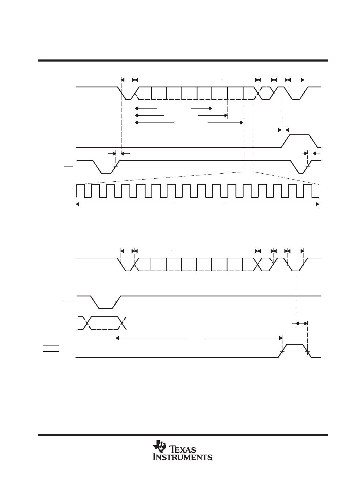
SLLS397 – NOVEMBER 1999
1
POST OFFICE BOX 655303 • DALLAS, TEXAS 75265
D
ST16C654 Pin Compatible With Additional
Enhancements
D
Supports Up To 24-MHz Crystal Input Clock
( 1.5 Mbps)
D
Supports Up To 48-MHz Oscillator Input
Clock ( 3 Mbps) for 5-V Operation
D
Supports Up To 32-MHz Oscillator Input
Clock ( 2 Mbps) for 3.3-V Operation
D
64-Byte Transmit FIFO
D
64-Byte Receive FIFO With Error Flags
D
Programmable and Selectable Transmit and
Receive FIFO Trigger Levels for DMA and
Interrupt Generation
D
Programmable Receive FIFO Trigger Levels
for Software/Hardware Flow Control
D
Software/Hardware Flow Control
– Programmable Xon/Xoff Characters
– Programmable Auto-RTS
and Auto-CTS
D
Optional Data Flow Resume by Xon Any
Character
D
DMA Signalling Capability for Both
Received and Transmitted Data
D
Supports 3.3-V or 5-V Supply
D
Characterized for Operation From –40°C to
85°C
D
Software Selectable Baud Rate Generator
D
Prescalable Provides Additional Divide by 4
Function
D
Fast Access 2 Clock Cycle IOR/IOW Pulse
Width
D
Programmable Sleep Mode
D
Programmable Serial Interface
Characteristics
– 5, 6, 7, or 8-Bit Characters
– Even, Odd, or No Parity Bit Generation
and Detection
– 1, 1.5, or 2 Stop Bit Generation
D
False Start Bit Detection
D
Complete Status Reporting Capabilities in
Both Normal and Sleep Mode
D
Line Break Generation and Detection
D
Internal Test and Loopback Capabilities
D
Fully Prioritized Interrupt System Controls
D
Modem Control Functions (CTS, RTS, DSR,
DTR
, RI, and CD)
22 23
NC
DSRD
CTSD
DTRD
GND
RTSD
INTD
CSD
TXD
IOR
TXC
CSC
INTC
RTSC
V
CC
DTRC
CTSC
DSRC
NC
NC
60
59
58
57
56
55
54
53
52
51
50
49
48
47
46
45
44
43
42
41
24
1
2
3
4
5
6
7
8
9
10
11
12
13
14
15
16
17
18
19
20
NC
NC
DSRA
CTSA
DTRA
V
CC
RTSA
INTA
CSA
TXA
IOW
TXB
CSB
INTB
RTSB
GND
DTRB
CTSB
DSRB
NC
25 26 27 28
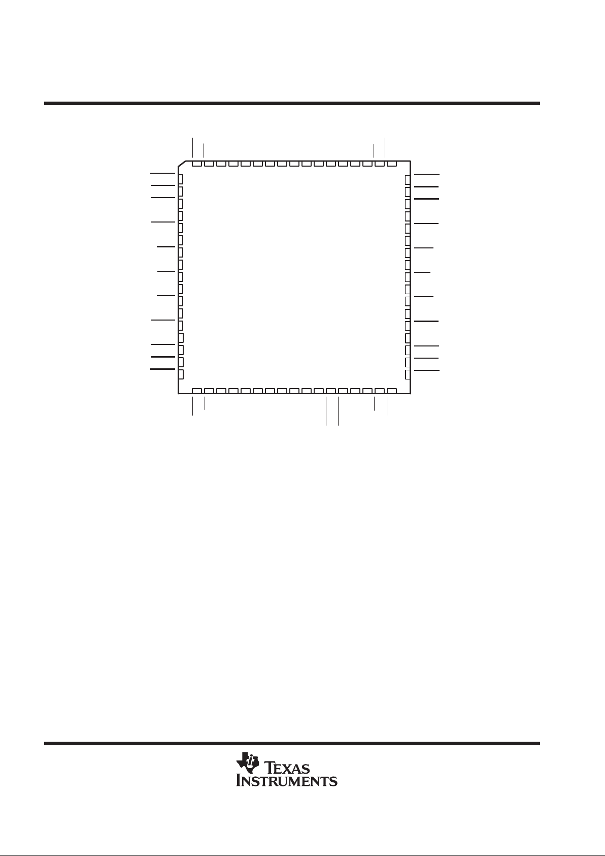
PN PACKAGE
(TOP VIEW)
D2
79 78 77 76 7580 74
RIA
RXA
GNDD7D6D5D4
XTAL1
RESET
CDB
RIB
RXB
CLKSEL
NC
A2
A1
72 71 7073
29
30 31 32 33
69 68
21
NC
D0
67 6665 64
34 35 36 37
RXRDY
TXRDY
GND
RXC
INTSEL
RXD
RID
NC
CDA
RIC
CDC
38 39 40
CDD
NC
63 62 61
V
CC
D1
NC
NC
XTAL2
NC
A0
D3
NC – No internal connection
TL16C754BPN
PRODUCTION DATA information is current as of publication date.
Products conform to specifications per the terms of Texas Instruments
standard warranty. Production processing does not necessarily include
testing of all parameters.
Please be aware that an important notice concerning availability, standard warranty, and use in critical applications of
Texas Instruments semiconductor products and disclaimers thereto appears at the end of this data sheet.
Copyright 1999, Texas Instruments Incorporated
TL16C754B
QUAD UART WITH 64-BYTE FIFO
SLLS397 – NOVEMBER 1999
2
POST OFFICE BOX 655303 • DALLAS, TEXAS 75265
28 29
DSRD
CTSD
DTRD
GND
RTSD
INTD
CSD
TXD
IOR
TXC
CSC
INTC
RTSC
VCC
DTRC
CTSC
DSRC
60
59
58
57
56
55
54
53
52
51
50
49
48
47
46
45
44
30
10
11
12
13
14
15
16
17
18
19
20
21
22
23
24
25
26
DSRA
CTSA
DTRA
VCC
RTSA
INTA
CSA
TXA
IOW
TXB
CSB
INTB
RTSB
GND
DTRB
CTSB
DSRB
31 32 33 34
D2
D1
87 6 5493
RXA
GNDD7D6D5D4
D3
XTAL2
RESET
RXRDY
TXRDY
RXB
CLKSEL
NC
A2A1A0
XTAL1
168672
35 36 37 38 39
66 65
27
CDB
RIB
D0
INTSEL
64 63 62 61
40 41 42 43
GND
RXC
RIC
CDC
VCC
RXD
RID
CDD
CDA
RIA
FN PACKAGE
(TOP VIEW)
TL16C754BFN
NC – No internal connection
description
The TL16C754B is a quad universal asynchronous receiver/transmitter (UART) with 64-byte FIFOs, automatic
hardware/software flow control, and data rates up to 3 Mbps. The TL16C754B offers enhanced features. It has
a transmission control register (TCR) that stores received FIFO threshold level to start/stop transmission during
hardware and software flow control. With the FIFO RDY register, the software gets the status of TXRDY/RXRDY
for all four ports in one access. On-chip status registers provide the user with error indications, operational
status, and modem interface control. System interrupts may be tailored to meet user requirements. An internal
loopback capability allows onboard diagnostics.
The UART transmits data sent to it from the peripheral 8-bit bus on the TX signal and receives characters on
the RX signal. Characters can be programmed to be 5, 6, 7, or 8 bits. The UART has a 64-byte receive FIFO
and transmit FIFO and can be programmed to interrupt at different trigger levels. The UART generates its own
desired baud rate based upon a programmable divisor and its input clock. It can transmit even, odd, or no parity
and 1, 1.5, or 2 stop bits. The receiver can detect break, idle or framing errors, FIFO overflow, and parity errors.
The transmitter can detect FIFO underflow. The UART also contains a software interface for modem control
operations, and software flow control and hardware flow control capabilities.
The TL16C754B is available in 80-pin TQFP and 68-pin PLCC packages.
TL16C754B
QUAD UART WITH 64-BYTE FIFO
SLLS397 – NOVEMBER 1999
3
POST OFFICE BOX 655303 • DALLAS, TEXAS 75265
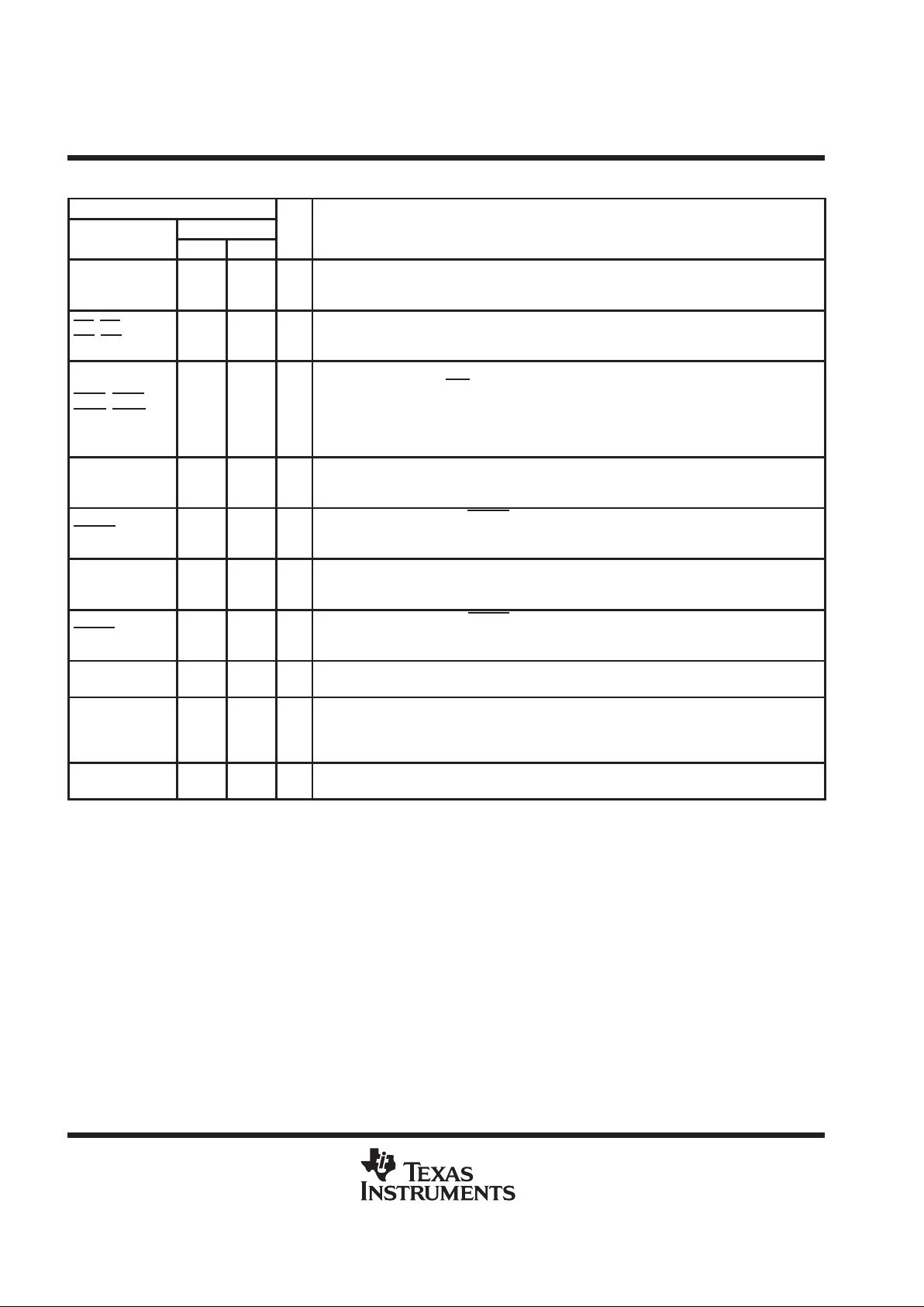
Terminal Functions
TERMINAL
NO.
I/O DESCRIPTION
NAME
PN FN
A0 30 34 I Address bit 0 select. Internal registers address selection. Refer to T able 7 for Register Address Map.
A1 29 33 I Address bit 1 select. Internal registers address selection. Refer to T able 7 for Register Address Map
A2 28 32 I Address bit 2 select. Internal registers address selection. Refer to T able 7 for Register Address Map
CDA, CDB
CDC, CDD
79, 23
39, 63
9, 27
43, 61
I
Carrier detect (active low). These inputs are associated with individual UART channels A through
D. A low on these pins indicates that a carrier has been detected by the modem for that channel.
CLKSEL 26 30 I
Clock select. CLKSEL selects the divide-by-1 or divide-by-4 prescalable clock. During the reset,
a logic 1 (VCC) on CLKSEL selects the divide-by-1 prescaler . A logic 0 (GND) on CLKSEL selects
the divide-by-4 prescaler. The value of CLKSEL is latched into MCR[7] at the trailing edge of RESET.
A logic 1 (VCC) on CLKSEL will latch a 0 into MCR[7]. A logic 0 (GND) on CLKSEL will latch a 1 into
MCR[7]. MCR[7] can be changed after RESET to alter the prescaler value.
CSA, CSB
CSC, CSD
9, 13,
49, 53
16, 20,
50, 54
I
Chip select A, B, C, and D (active low). These pins enable data transfers between the user CPU
and the TL16C754B for the channel(s) addressed. Individual UART sections (A, B, C, D) are
addressed by providing a low on the respective CSA
through CSD pin.
CTSA, CTSB
CTSC, CTSD
4, 18
44, 58
11, 25
45, 59
I
Clear to send (active low). These inputs are associated with individual UART channels A through
D. A low on the CTS pins indicates the modem or data set is ready to accept transmit data from the
754A. Status can be checked by reading MSR bit 4. These pins only affect the transmit and receive
operations when auto CTS function is enabled through the enhanced feature register (EFR) bit 7,
for hardware flow control operation.
D0–D2
D3–D7
68–70,
71–75
66–68,
1–5
I/O
Data bus (bidirectional). These pins are the eight bit, 3-state data bus for transferring information
to or from the controlling CPU. D0 is the least significant bit and the first data bit in a transmit or
receive serial data stream.
DSRA, DSRB
DSRC, DSRD
3, 19
43, 59
10, 26
44, 60
I
Data set ready (active low). These inputs are associated with individual UART channels A through
D. A low on these pins indicates the modem or data set is powered on and is ready for data exchange
with the UART.
DTRA, DTRB
DTRC, DTRD
5, 17
45, 57
12, 24
46, 58
O
Data terminal ready (active low). These outputs are associated with individual UART channels A
through D. A low on these pins indicates that the 754A is powered on and ready. These pins can
be controlled through the modem control register. Writing a 1 to MCR bit 0 sets the DTR
output to
low, enabling the modem. The output of these pins is high after writing a 0 to MCR bit 0, or after a
reset.
GND
16, 36,
56, 76
6, 23,
40, 57
Pwr Signal and power ground
INTA, INTB
INTC, INTD
8, 14,
48, 54
15, 21,
49, 55
O
Interrupt A, B, C, and D (active high). These pins provide individual channel interrupts, INTA-D.
INTA–D are enabled when MCR bit 3 is set to a 1, interrupts are enabled in the interrupt enable
register (IER) and when an interrupt condition exists. Interrupt conditions include: receiver errors,
available receiver buffer data, transmit buffer empty, or when a modem status flag is detected.
INTA–D are in the high-impedance state after reset.
INTSEL 67 65 I
Interrupt select (active high with internal pulldown). INTSEL can be used in conjunction with MCR
bit 3 to enable or disable the 3-state interrupts INTA-D or override MCR bit 3 and force continuous
interrupts. Interrupt outputs are enabled continuously by making this pin a 1. Driving this pin low
allows MCR bit 3 to control the 3-state interrupt output. In this mode, MCR bit 3 is set to a 1 to enable
the 3-state outputs.
IOR 51 52 I
Read input (active low strobe). A valid low level on IOR will load the contents of an internal register
defined by address bits A0–A2 onto the TL16C754B data bus (D0–D7) for access by an external
CPU.
IOW 11 18 I
Write input (active low strobe). A valid low level on IOW will transfer the contents of the data bus
(D0–D7) from the external CPU to an internal register that is defined by address bits A0–A2.
TL16C754B
QUAD UART WITH 64-BYTE FIFO
SLLS397 – NOVEMBER 1999
4
POST OFFICE BOX 655303 • DALLAS, TEXAS 75265
Terminal Functions (Continued)
TERMINAL
NO.
I/O DESCRIPTION
NAME
PN FN
RESET 33 37 I
Reset. RESET will reset the internal registers and all the outputs. The UART transmitter output
and the receiver input will be disabled during reset time. See TL16C754B external reset
conditions for initialization details. RESET is an active high input.
RIA, RIB
RIC, RID
78, 24
38, 64
8, 28
42, 62
I
Ring indicator (active low). These inputs are associated with individual UART channels A through
D. A low on these pins indicates the modem has received a ringing signal from the telephone line.
A low to high transition on these input pins generates a modem status interrupt, if it is enabled.
RTSA, RTSB
RTSC, RTSD
7, 15
47, 55
14, 22
48, 56
O
Request to send (active low). These outputs are associated with individual UART channels A
through D. A low on the RTS
pins indicates the transmitter has data ready and waiting to send.
Writing a 1 in the modem control register (MCR bit 1) sets these pins to low, indicating data is
available. After a reset, these pins are set to 1. These pins only affects the transmit and receive
operation when auto RTS function is enabled through the enhanced feature register (EFR) bit 6,
for hardware flow control operation.
RXA, RXB
RXC, RXD
77, 25
37, 65
7, 29
41, 63
I
Receive data input. These inputs are associated with individual serial channel data to the 754A.
During the local loopback mode, these RX input pins are disabled and TX data is internally
connected to the UART RX input internally.
RXRDY 34 38 O
Receive ready (active low). RXRDY contains the wire-ORed status of all four receive channel
FIFOs, RXRDY A–D. It goes low when the trigger level has been reached or a timeout interrupt
occurs. It goes high when all RX FIFOs are empty and there is an error in RX FIFO.
TXA, TXB
TXC, TXD
10, 12
50, 52
17, 19
51, 53
O
Transmit data. These outputs are associated with individual serial transmit channel data from the
754A. During the local loopback mode, the TX input pin is disabled and TX data is internally
connected to the UART RX input.
TXRDY 35 39 O
Transmit ready (active low). TXRDY contains the wire-ORed status of all four transmit channel
FIFOs, TXRDY A–D. It goes low when there are a trigger level number of spares available. It goes
high when all four TX buffers are full.
V
CC
6, 46,6613, 47,
64
Pwr Power supply inputs
XTAL1 31 35 I
Crystal or external clock input. XTAL1 functions as a crystal input or as an external clock input.
A crystal can be connected between XTAL1 and XTAL2 to form an internal oscillator circuit (see
Figure 10). Alternatively, an external clock can be connected to XTAL1 to provide custom data
rates.
XTAL2 32 36 O
Output of the crystal oscillator or buffered clock. See also XTAL1. XTAL2 is used as a crystal
oscillator output or buffered clock output.
TL16C754B
QUAD UART WITH 64-BYTE FIFO
SLLS397 – NOVEMBER 1999
5
POST OFFICE BOX 655303 • DALLAS, TEXAS 75265
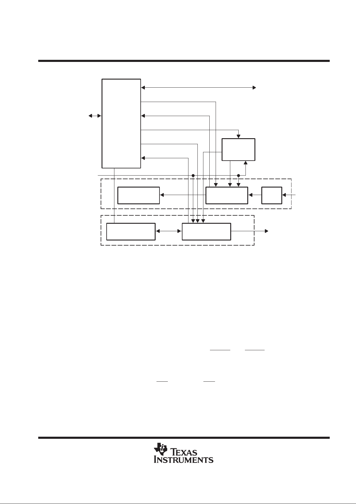
functional block diagram
Control Signals
Modem Control Signals
Divisor
Bus
Interface
Control
and
Status Block
Status Signals
Control Signals
Status Signals
Baud-Rate
Generator
UART_CLK
Receiver Block
Logic
Receiver FIFO
64-Byte
Vote
Logic
Transmitter Block
Logic
Transmitter FIFO
64-Byte
RX
RX
TX
TX
NOTE: The Vote logic determines whether the RX data is a logic 1 or 0. It takes three samples of the RX line and uses a majority vote to determine
the logic level received. The Vote logic operates on all bits received.
functional description
The TL16C754B UART is pin compatible with the TL16C554 and ST16C654 UART s. It provides more enhanced
features. All additional features are provided through a special enhanced feature register.
The UART will perform serial-to-parallel conversion on data characters received from peripheral devices or
modems and parallel-to-parallel conversion on data characters transmitted by the processor. The complete
status of each channel of the TL16C754B UART can be read at any time during functional operation by the
processor.
The TL16C754B UART can be placed in an alternate mode (FIFO mode) relieving the processor of excessive
software overhead by buffering received/transmitted characters. Both the receiver and transmitter FIFOs can
store up to 64 bytes (including three additional bits of error status per byte for the receiver FIFO) and have
selectable or programmable trigger levels. Primary outputs RXRDY
and TXRDY allow signalling of DMA
transfers.
The TL16C754B UART has selectable hardware flow control and software flow control. Both schemes
significantly reduce software overhead and increase system efficiency by automatically controlling serial data
flow. Hardware flow control uses the RTS output and CTS input signals. Software flow control uses
programmable Xon/Xoff characters.
The UART will include a programmable baud rate generator that can divide the timing reference clock input by
a divisor between 1 and (216–1). The CLKSEL pin can be used to divide the input clock by 4 or by 1 to generate
the reference clock during the reset. The divide-by-4 clock is selected when CLKSEL pin is a logic 0 or the
divide-by-1 is selected when CLKSEL is a logic 1.
TL16C754B
QUAD UART WITH 64-BYTE FIFO
SLLS397 – NOVEMBER 1999
6
POST OFFICE BOX 655303 • DALLAS, TEXAS 75265
functional description (continued)
trigger levels
The TL16C754B UART provides independent selectable and programmable trigger levels for both receiver and
transmitter DMA and interrupt generation. After reset, both transmitter and receiver FIFOs are disabled and so,
in effect, the trigger level is the default value of one byte. The selectable trigger levels are available via the FCR.
The programmable trigger levels are available via the TLR.
hardware flow control
Hardware flow control is composed of auto-CTS and auto-RTS. Auto-CTS and auto-RTS can be
enabled/disabled independently by programming EFR[7:6].
With auto-CTS, CTS must be active before the UART can transmit data.
Auto-RTS
only activates the RTS output when there is enough room in the FIFO to receive data and deactivates
the RTS
output when the RX FIFO is sufficiently full. The HALT and RESTORE trigger levels in the TCR
determine the levels at which RTS is activated/deactivated.
If both auto-CTS
and auto-RTS are enabled, when RTS is connected to CTS, data transmission does not occur
unless the receiver FIFO has empty space. Thus, overrun errors are eliminated during hardware flow control.
If not enabled, overrun errors occur if the transmit data rate exceeds the receive FIFO servicing latency.
auto-RTS
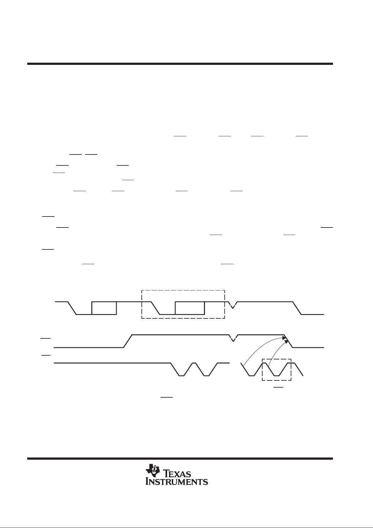
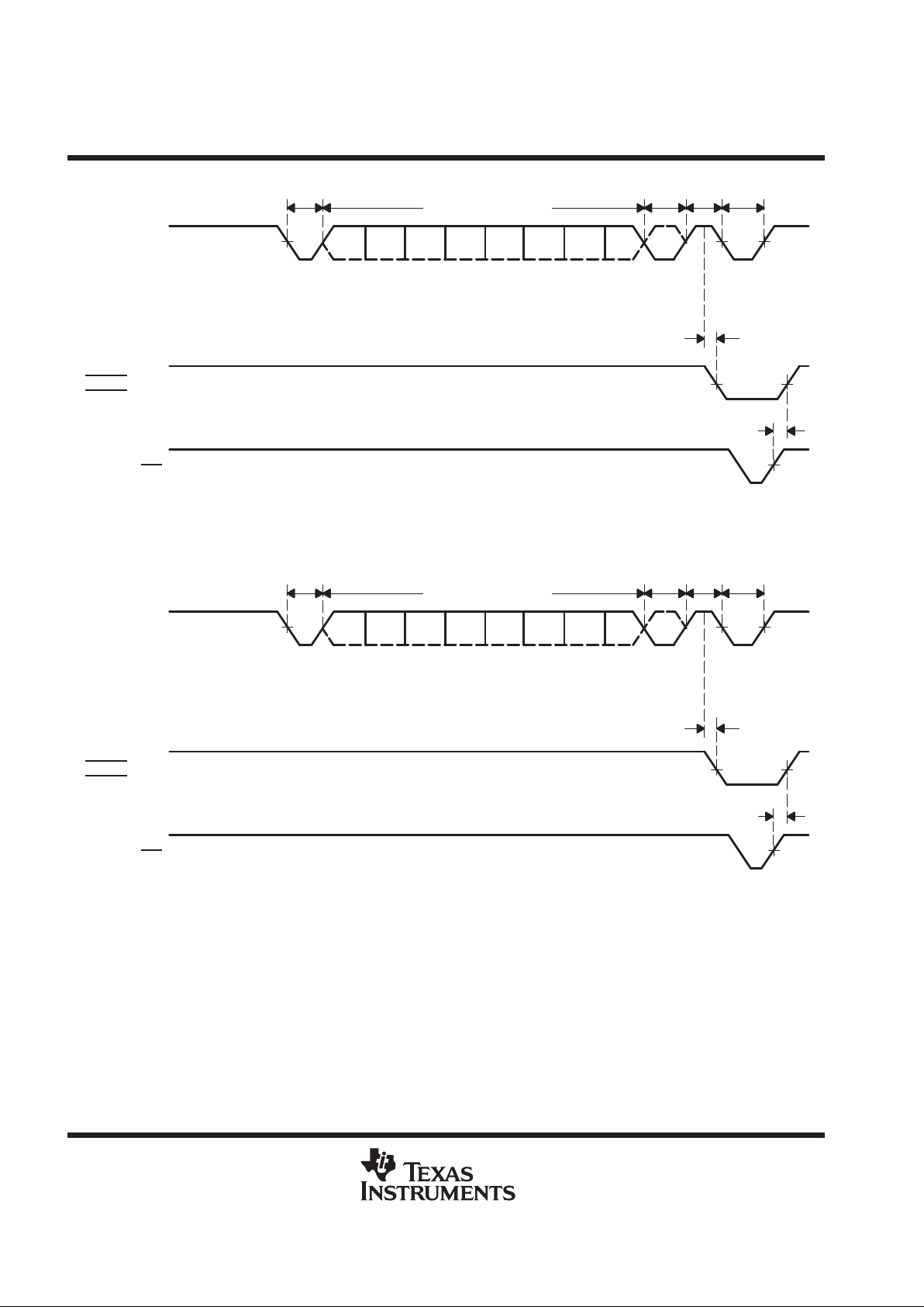
Auto-RTS data flow control originates in the receiver block (see functional block diagram). Figure 1 shows RTS
functional timing. The receiver FIFO trigger levels used in Auto-RTS are stored in the TCR. RTS is active if the
RX FIFO level is below the HAL T trigger level in TCR[3:0]. When the receiver FIFO HALT trigger level is reached,
RTS
is deasserted. The sending device (e.g., another UART) may send an additional byte after the trigger level
is reached (assuming the sending UART has another byte to send) because it may not recognize the
deassertion of RTS until it has begun sending the additional byte. RTS is automatically reasserted once the
receiver FIFO reaches the RESUME trigger level programmed via TCR[7:4]. This reassertion allows the
sending device to resume transmission.
RX
RTS
IOR
Start Byte N Stop Start Byte N+1 Stop Start
1 2 N N+1
NOTES: A. N = receiver FIFO trigger level
B. The two blocks in dashed lines cover the case where an additional byte is sent as described in Auto-RTS
.
Figure 1. RTS Functional Timing
TL16C754B
QUAD UART WITH 64-BYTE FIFO
SLLS397 – NOVEMBER 1999
7
POST OFFICE BOX 655303 • DALLAS, TEXAS 75265
functional description (continued)
auto-CTS
The transmitter circuitry checks CTS before sending the next data byte. When CTS is active, the transmitter
sends the next byte. To stop the transmitter from sending the following byte, CTS must be deasserted before
the middle of the last stop bit that is currently being sent. The auto-CTS function reduces interrupts to the host
system. When flow control is enabled, the CTS
state changes and need not trigger host interrupts because the
device automatically controls its own transmitter. Without auto-CTS, the transmitter sends any data present in
the transmit FIFO and a receiver overrun error can result. Figure 2 shows CTS functional timing, and Figure 3
shows an example of autoflow control.
Byte 0–7 StopStart Byte 0–7 StopStart
TX
CTS
NOTES: A. When CTS is low, the transmitter keeps sending serial data out.
B. When CTS
goes high before the middle of the last stop bit of the current byte, the transmitter finishes sending the current byte, but
it does not send the next byte.
C. When CTS
goes from high to low, the transmitter begins sending data again.
Figure 2. CTS Functional Timing
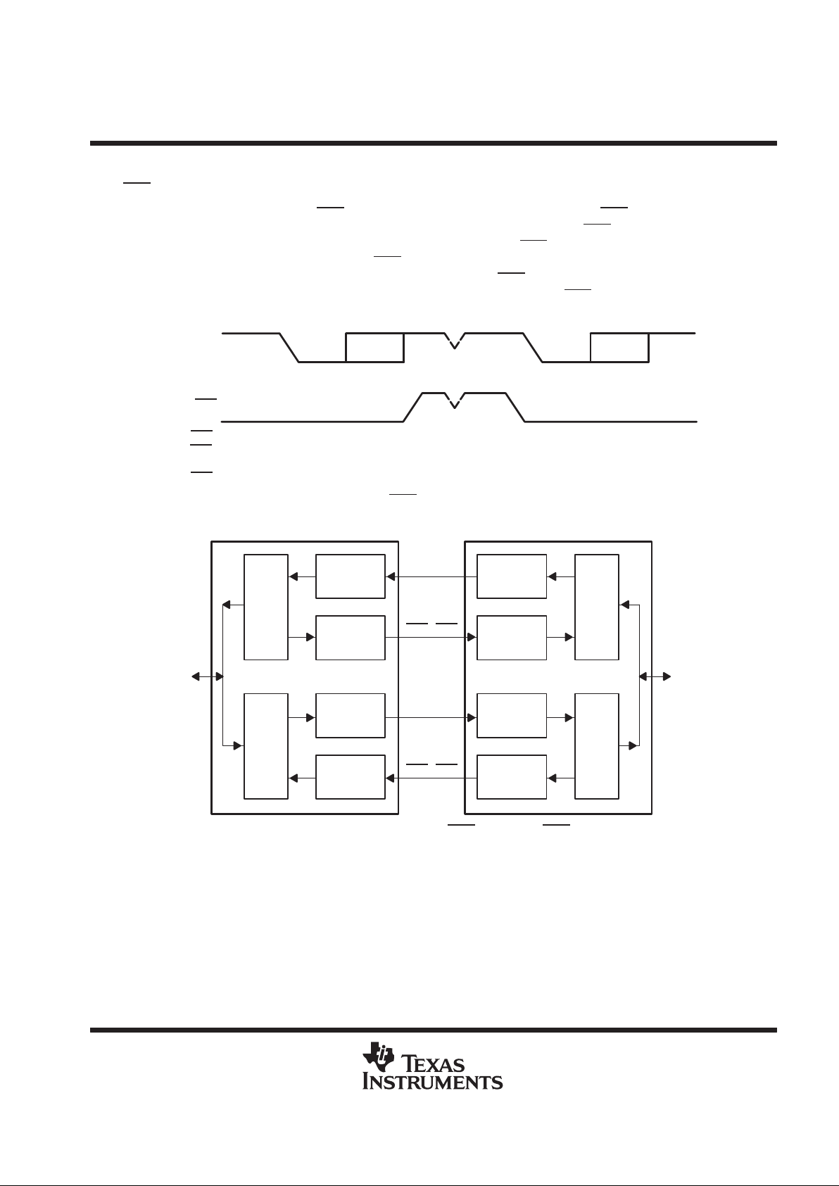
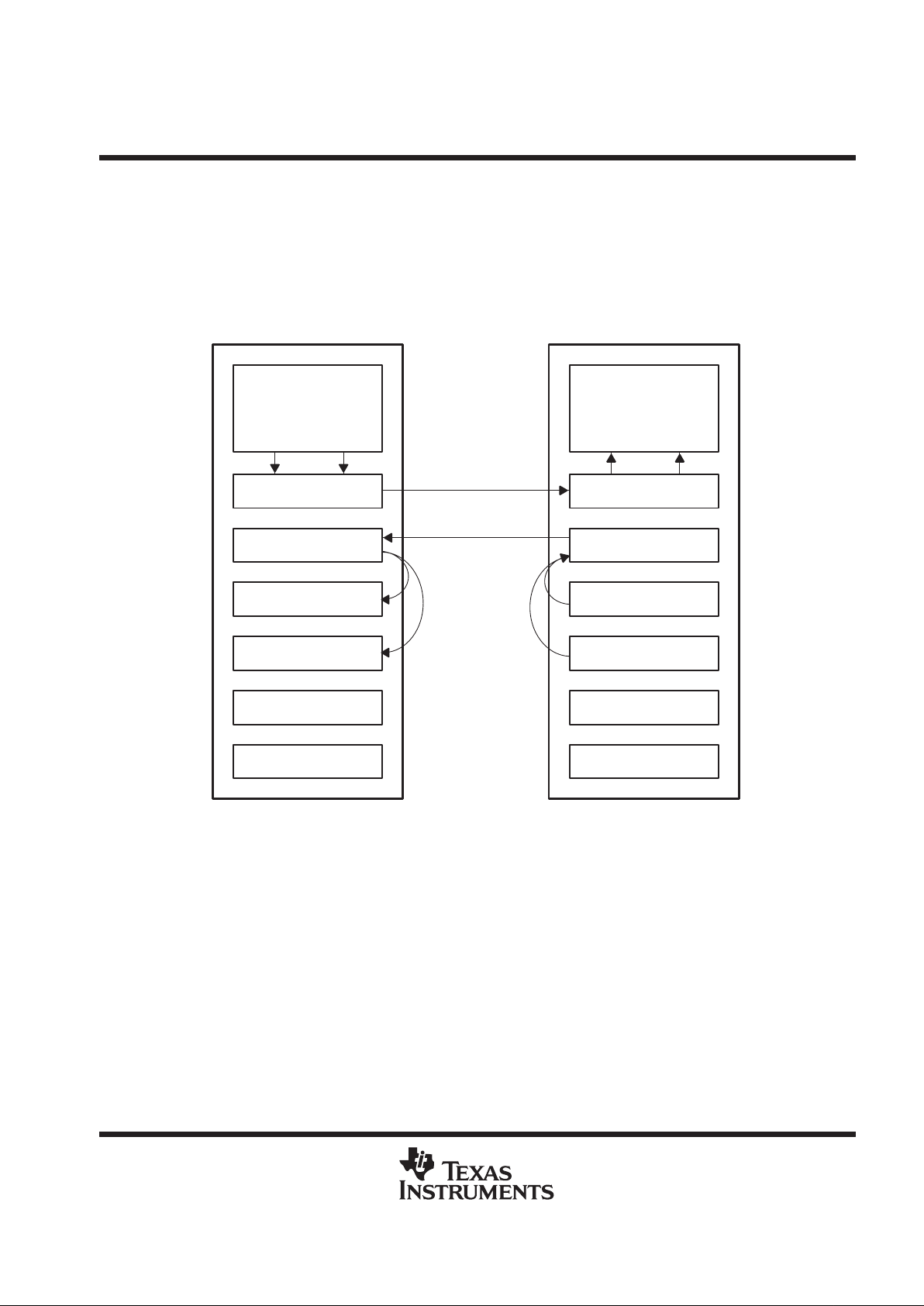
Serial to
Parallel
Flow
Control
Parallel to
Serial
Flow
Control
RX
FIFO
TX
FIFO
Parallel to
Serial
Flow
Control
Serial to
Parallel
Flow
Control
TX
FIFO
RX
FIFO
D7–D0 D7–D0
UART 1 UART 2
RX
RTS
TX
CTS
TX
CTS
RX
RTS
Figure 3. Autoflow Control (Auto-RTS and Auto-CTS) Example
software flow control
Software flow control is enabled through the enhanced feature register and the modem control register. Different
combinations of software flow control can be enabled by setting different combinations of EFR[3–0]. Table 1
shows software flow control options.
Two other enhanced features relate to S/W flow control:
– Xon Any Function [MCR(5): Operation will resume after receiving any character after recognizing the
Xoff character.
TL16C754B
QUAD UART WITH 64-BYTE FIFO
SLLS397 – NOVEMBER 1999
8
POST OFFICE BOX 655303 • DALLAS, TEXAS 75265
functional description (continued)
NOTE:
It is possible that an Xon1 character is recognized as an Xon Any character, which could
cause an Xon2 character to be written to the RX FIFO.
– Special Character [EFR(5)]: Incoming data is compared to Xoff2. Detection of the special character
sets the Xoff interrupt {IIR(4)] but does not halt transmission. The Xoff interrupt is cleared by a read of the
IIR. The special character is transferred to the RX FIFO.
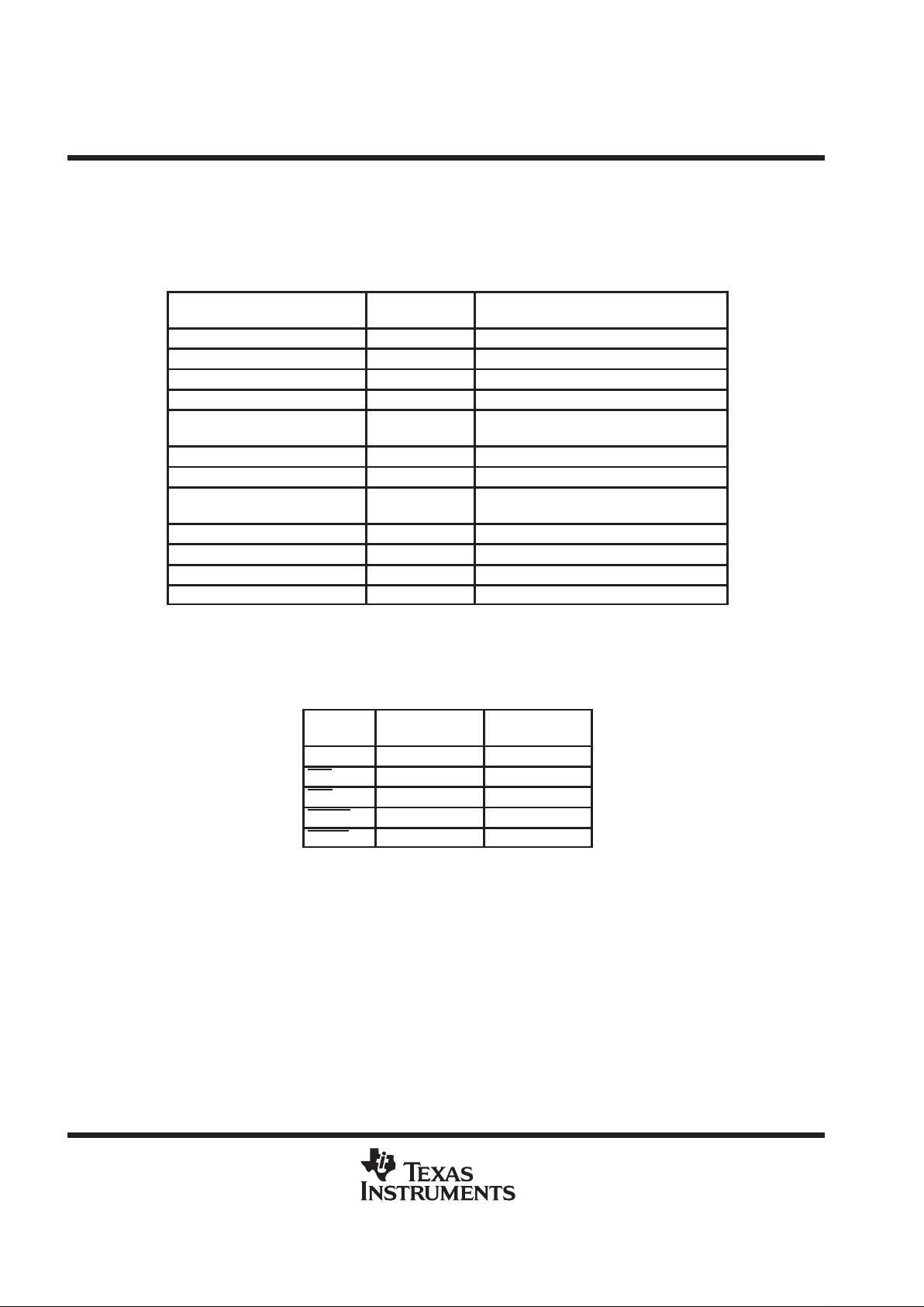
Table 1. Software Flow Control Options EFR[3:0]
BIT 3 BIT 2 BIT 1 BIT 0 Tx, Rx SOFTWARE FLOW CONTROLS
0 0 X X No transmit flow control
1 0 X X Transmit Xon1, Xoff1
0 1 X X Transmit Xon2, Xoff2
1 1 X X Transmit Xon1, Xon2: Xoff1, Xoff2
X X 0 0 No receive flow control
X X 1 0 Receiver compares Xon1, Xoff1
X X 0 1 Receiver compares Xon2, Xoff2
1 0 1 1 Transmit Xon1, Xoff1
Receiver compares Xon1 or Xon2, Xoff1 or Xoff2
0 1 1 1 Transmit Xon2, Xoff2
Receiver compares Xon1 or Xon2, Xoff1 or Xoff2
1 1 1 1 Transmit Xon1, Xon2: Xoff1, Xoff2
Receiver compares Xon1 and Xon2: Xoff1 and Xoff2
0 0 1 1 No transmit flow control
Receiver compares Xon1 and Xon2: Xoff1 and Xoff2
When software flow control operation is enabled, the TL16C754B will compare incoming data with Xoff1/2
programmed characters (in certain cases Xoff1 and Xoff2 must be received sequentially1). When an Xoff
character is received, transmission is halted after completing transmission of the current character. Xoff
character detection also sets IIR[4] and causes INT to go high (if enabled via IER[5]).
To resume transmission an Xon1/2 character must be received (in certain cases Xon1 and Xon2 must be
received sequentially). When the correct Xon characters are received IIR[4] is cleared and the Xoff interrupt
disappears.
NOTE:
If a parity, framing or break error occurs while receiving a software flow control character, this
character will be treated as normal data and will be written to the RCV FIFO.
Xoff1/2 characters are transmitted when the RX FIFO has passed the programmed trigger level TCR[3:0].
Xon1/2 characters are transmitted when the RX FIFO reaches the trigger level programmed via TCR[7:4].
An important note here is that if, after an Xoff character has been sent, software flow control is disabled, the
UART will transmit Xon characters automatically to enable normal transmission to proceed. A feature of the
TL16C754B UART design is that if the software flow combination (EFR[3:0]) changes after an Xoff has been
sent, the originally programmed Xon is automatically sent. If the RX FIFO is still above the trigger level the newly
programmed Xoff1/2 will be transmitted.
1. When pairs of Xon/Xoff characters are programmed to occur sequentially, received Xon1/Xoff1 characters will be written to the Rx FIFO if
the subsequent character is not Xon2/Xoff2.
TL16C754B
QUAD UART WITH 64-BYTE FIFO
SLLS397 – NOVEMBER 1999
9
POST OFFICE BOX 655303 • DALLAS, TEXAS 75265
functional description (continued)
The transmission of Xoff/Xon(s) follows the exact same protocol as transmission of an ordinary byte from the
FIFO. This means that even if the word length is set to be 5, 6, or 7 characters then the 5, 6, or 7 least significant
bits of Xoff1,2/Xon1,2 will be transmitted. The transmission of 5, 6, or 7 bits of a character is seldom done, but
this functionality is included to maintain compatibility with earlier designs.
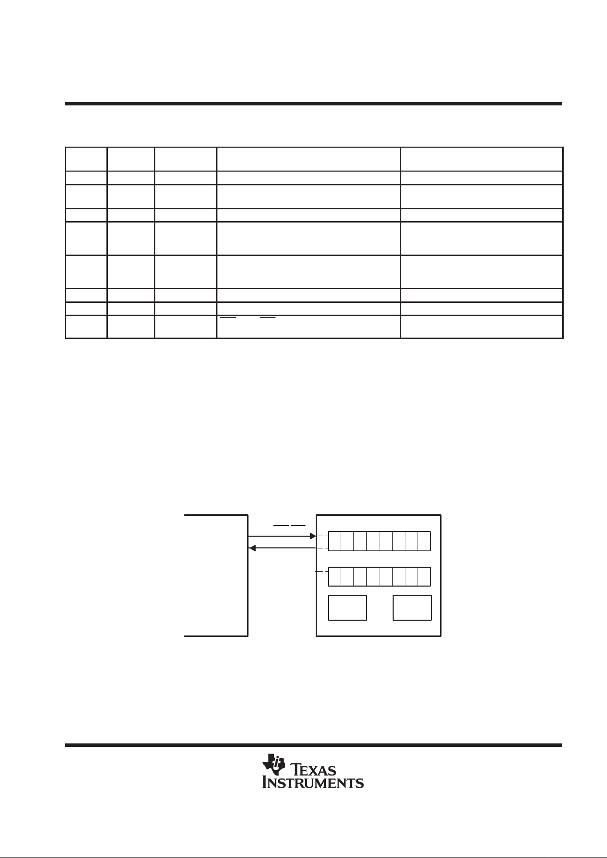
It is assumed that software flow control and hardware flow control will never be enabled simultaneously . Figure 4
shows a software flow control example.
UART 1
Parallel to Serial
Serial to Parallel
Xon-1 Word
Xon-2 Word
Xoff-1 Word
Xoff-1 Word
Transmit
FIFO
Serial to Parallel
Parallel to Serial
Xon-1 Word
Xon-2 Word
Xoff-1 Word
Xoff-2 Word
Receive
FIFO
Data
Xoff – Xon – Xoff
Compare
Programmed
Xon–Xoff
Characters
UART 2
Figure 4. Software Flow Control Example
software flow control example
Assumptions: UART1 is transmitting a large text file to UART2. Both UARTs are using software flow control with
single character Xoff (0F) and Xon (0D) tokens. Both have Xoff threshold (TCR [3:0]=F) set to 60 and Xon
threshold (TCR[7:4]=8) set to 32. Both have the interrupt receive threshold (TLR[7:4]=D) set to 52.
UART1 begins transmission and sends 52 characters, at which point UART2 will generate an interrupt to its
processor to service the RCV FIFO, but assume the interrupt latency is fairly long. UART1 will continue sending
characters until a total of 60 characters have been sent. At this time UART2 will transmit a 0F to UART1,
informing UART1 to halt transmission. UART1 will likely send the 61
st
character while UART2 is sending the
Xoff character . Now UART2 is serviced and the processor reads enough data out of the RCV FIFO that the level
drops to 32. UART2 will now send a 0D to UART1, informing UART1 to resume transmission.
TL16C754B
QUAD UART WITH 64-BYTE FIFO
SLLS397 – NOVEMBER 1999
10
POST OFFICE BOX 655303 • DALLAS, TEXAS 75265
functional description (continued)
reset
Table 2 summarizes the state of registers after reset.
Table 2. Register Reset Functions
REGISTER
RESET
CONTROL
RESET STATE
Interrupt enable register RESET All bits cleared
Interrupt identification register RESET Bit 0 is set. All other bits cleared.
FIFO control register RESET All bits cleared
Line control register RESET Reset to 00011101 (1D hex).
Modem control register RESET
Bit 6–0 cleared. Bit 7 reflects the inverse of
the CLKSEL pin value.
Line status register RESET Bits 5 and 6 set. All other bits cleared.
Modem status register RESET Bits 0–3 cleared. Bits 4–7 input signals.
Enhanced feature register RESET
Bit 6 – 0 is cleared. Bit 7 reflects the inverse
of the CLKSEL pin value.
Receiver holding register RESET Pointer logic cleared
Transmitter holding register RESET Pointer logic cleared
Transmission control register RESET All bits cleared
Trigger level register RESET All bits cleared
NOTE: Registers DLL, DLH, SPR, Xon1, Xon2, Xoff1, Xoff2 are not reset by the top-level reset signal
RESET, i.e., they hold their initialization values during reset.
Table 3 summarizes the state of some signals after reset.
Table 3. Signal Reset Functions
SIGNAL
RESET
CONTROL
RESET STATE
TX RESET High
RTS RESET High
DTR RESET High
RXRDY RESET High
TXRDY RESET Low
interrupts
The TL16C754B UART has interrupt generation and prioritization (6 prioritized levels of interrupts) capability.
The interrupt enable register (IER) enables each of the 6 types of interrupts and the INT signal in response to
an interrupt generation. The IER can also disable the interrupt system by clearing bits 0–3, 5–7. When an
interrupt is generated, the interrupt identification register(IIR) indicates that an interrupt is pending and provides
the type of interrupt through IIR[5–0]. Table 4 summarizes the interrupt control functions.
TL16C754B
QUAD UART WITH 64-BYTE FIFO
SLLS397 – NOVEMBER 1999
11
POST OFFICE BOX 655303 • DALLAS, TEXAS 75265
functional description (continued)
Table 4. Interrupt Control Functions
IIR[5–0]
PRIORITY
LEVEL
INTERRUPT
TYPE
INTERRUPT SOURCE INTERRUPT RESET METHOD
000001 None None None None
000110 1 Receiver line
status
OE, FE, PE, or BI errors occur in characters in the
RX FIFO
FE< PE< BI: All erroneous characters are
read from the RX FIFO. OE: Read LSR
001100 2 RX timeout Stale data in RX FIFO Read RHR
000100 2 RHR interrupt DRDY (data ready)
(FIFO disable)
RX FIFO above trigger level (FIFO enable)
Read RHR
000010 3 THR interrupt TFE (THR empty)
(FIFO disable)
TX FIFO passes above trigger level (FIFO enable)
Read IIR OR a write to the THR
000000 4 Modem status MSR[3:0]= 0 Read MSR
010000 5 Xoff interrupt Receive Xoff character(s)/special character Receive Xon character(s)/Read of IIR
100000 6 CTS, RTS RTS pin or CTS pin change state from active (low)
to inactive (high)
Read IIR
It is important to note that for the framing error, parity error , and break conditions, LSR[7] generates the interrupt.
LSR[7] is set when there is an error anywhere in the RX FIFO and is cleared only when there are no more errors
remaining in the FIFO. LSR[4–2] always represent the error status for the received character at the top of the
Rx FIFO. Reading the Rx FIFO updates LSR[4–2] to the appropriate status for the new character at the top of
the FIFO. If the Rx FIFO is empty, then LSR[4–2] is all zeros.
For the Xoff interrupt, if an Xoff flow character detection caused the interrupt, the interrupt is cleared by an Xon
flow character detection. If a special character detection caused the interrupt, the interrupt is cleared by a read
of the ISR.
interrupt mode operation
In interrupt mode (if any bit of IER[3:0] is1), the processor is informed of the status of the receiver and transmitter
by an interrupt signal, INT. Therefore, it is not necessary to continuously poll the line status register (LSR) to
see if any interrupt needs to be serviced. Figure 5 shows interrupt mode operation.
1111
IER
IIR
THR RHR
IOW/IOR
INTProcessor
Figure 5. Interrupt Mode Operation
polled mode operation
In polled mode (IER[3:0] = 0000), the status of the receiver and transmitter can then be checked by polling the
line status register (LSR). This mode is an alternative to the interrupt mode of operation where the status of the
receiver and transmitter is automatically known by means of interrupts sent to the CPU. Figure 6 shows polled
mode operation.
TL16C754B
QUAD UART WITH 64-BYTE FIFO
SLLS397 – NOVEMBER 1999
12
POST OFFICE BOX 655303 • DALLAS, TEXAS 75265
functional description (continued)
0000
LSR
IER
THR RHR
IOW/IOR
Processor
Figure 6. FIFO Polled Mode Operation
DMA signalling
There are two modes of DMA operation, DMA mode 0 or 1, selected by FCR[3].
In DMA mode 0 or FIFO disable (FCR[0]=0) DMA occurs in single character transfers. In DMA mode 1
multicharacter (or block) DMA transfers are managed to relieve the processor for longer periods of time.
single DMA transfers (DMA mode0/FIFO disable)
Transmitter: When empty, the TXRDY signal becomes active. TXRDY will go inactive after one character has
been loaded into it.
Receiver: RXRDY is active when there is at least one character in the FIFO. It becomes inactive when the
receiver is empty.
Figure 7 shows TXRDY and RXRDY in DMA mode 0/FIFO disable.
FIFO Empty
TXRDY
wrptr
TXRDY
wrptr
At Least One
Location Filled
TX
FIFO Empty
RXRDY
rdptr
RXRDY
rdptr
At Least One
Location Filled
RX
Figure 7. TXRDY and RXRDY in DMA Mode 0/FIFO Disable
block DMA transfers (DMA mode 1)
Transmitter: TXRDY is active when a trigger level number of spaces are available. It becomes inactive when
the FIFO is full.

TL16C754B
QUAD UART WITH 64-BYTE FIFO
SLLS397 – NOVEMBER 1999
13
POST OFFICE BOX 655303 • DALLAS, TEXAS 75265
functional description (continued)
Receiver: RXRDY becomes active when the trigger level has been reached or when a timeout interrupt occurs.
It will go inactive when the FIFO is empty or an error in the RX FIFO is flagged by LSR(7)
Figure 8 shows TXRDY and RXRDY in DMA mode 1.
TXRDY
wrptr
TXRDY
wrptr
FIFO Full
TX
FIFO Empty
RXRDY
rdptr
RXRDY
rdptr
At Least One
Location Filled
RX
Trigger
Level
Trigger
Level
Figure 8. TXRDY and RXRDY in DMA Mode 1
sleep mode
Sleep mode is an enhanced feature of the TL16C754B UART. It is enabled when EFR[4], the enhanced
functions bit, is set and when IER[4] is set. Sleep mode is entered when:
– The serial data input line, RX, is idle (see break and time-out conditions).
– The TX FIFO and TX shift register are empty.
– There are no interrupts pending except THR and timeout interrupts.
Sleep mode will not be entered if there is data in the RX FIFO.
In sleep mode the UART clock and baud rate clock are stopped. Since most registers are clocked using these
clocks the power consumption is greatly reduced. The UART will wake up when any change is detected on the
RX line, when there is any change in the state of the modem input pins or if data is written to the TX FIFO.
NOTE:
Writing to the divisor latches, DLL and DLH, to set the baud clock, must not be done during sleep
mode. Therefore it is advisable to disable sleep mode using IER[4] before writing to DLL or DLH.
break and timeout conditions
An RX timeout condition is detected when the receiver line, RX, has been high for a time equivalent to (4X
programmed word length)+12 bits and there is at least one byte stored in the Rx FIFO.
When a break condition occurs, the TX line is pulled low. A break condition is activated by setting LCR[6].

TL16C754B
QUAD UART WITH 64-BYTE FIFO
SLLS397 – NOVEMBER 1999
14
POST OFFICE BOX 655303 • DALLAS, TEXAS 75265
functional description (continued)
programmable baud rate generator
The TL16C754B UART contains a programmable baud generator that divides reference clock by a divisor in
the range between 1 and (216–1). The output frequency of the baud rate generator is 16x the baud rate. An
additional divide-by-4 prescaler is also available and can be selected by the CLKSEL pin or MCR[7], as shown
in the following. The formula for the divisor is:
Divisor = (XTAL1 crystal input frequency / prescaler) / (desired baud rate × 16)
Where
prescaler
+
ȥ
ȡ
Ȣ
1 when CLKSEL+high during reset, or MCR[7] is set to 0 after reset
4 when CLKSEL+low during reset, or MCR[7] is set to 1 after reset
Figure 9 shows the internal prescaler and baud rate generator circuitry.
Prescaler Logic
(Divide By 1)
Prescaler Logic
(Divide By 4)
Internal
Oscillator
Logic
Bandrate
Generator
Logic
XTAL1
XTAL2
Internal
Bandrate Clock
For Transmitter
and Receiver
MCR[7] = 0
MCR[7] = 1
Input Clock
Reference
Clock
Figure 9. Prescaler and Baud Rate Generator Block Diagram
DLL and DLH must be written to in order to program the baud rate. DLL and DLH are the least significant and
most significant byte of the baud rate divisor.
If DLL and DLH are both zero, the UART is effectively disabled, as no baud clock will be generated.
The programmable baud rate generator is provided to select both the transmit and receive clock rates.
Table 5 and Table 6 show the baud rate and divisor correlation for the crystal with frequency 1.8432 MHz and
3.072 MHz, respectively.

TL16C754B
QUAD UART WITH 64-BYTE FIFO
SLLS397 – NOVEMBER 1999
15
POST OFFICE BOX 655303 • DALLAS, TEXAS 75265
programmable baud rate generator (continued)
Table 5. Baud Rates Using a 1.8432-MHz Crystal
DESIRED
BAUD RATE
DIVISOR USED
TO GENERATE
16 × CLOCK
PERCENT ERROR
DIFFERENCE BETWEEN
DESIRED AND ACTUAL
50 2304
75 1536
110 1047 0.026
134.5 857 0.058
150 768
300 384
600 192
1200 96
1800 64
2000 58 0.69
2400 48
3600 32
4800 24
7200 16
9600 12
19200 6
38400 3
56000 2 2.86
Table 6. Baud Rates Using a 3.072-MHz Crystal
DESIRED
BAUD RATE
DIVISOR USED
TO GENERATE
16 × CLOCK
PERCENT ERROR
DIFFERENCE BETWEEN
DESIRED AND ACTUAL
50 3840
75 2560
110 1745 0.026
134.5 1428 0.034
150 1280
300 640
600 320
1200 160
1800 107 0.312
2000 96
2400 80
3600 53 0.628
4800 40
7200 27 1.23
9600 20
19200 10
38400 5

TL16C754B
QUAD UART WITH 64-BYTE FIFO
SLLS397 – NOVEMBER 1999
16
POST OFFICE BOX 655303 • DALLAS, TEXAS 75265
programmable baud generator (continued)
Figure 10 shows the crystal clock circuit reference.
Driver
Optional
Driver
External
Clock
Optional
Clock
Output
Oscillator Clock
to Baud Generator
Logic
XTAL1
XTAL2
V
CC
Crystal
XTAL1
RX2
V
CC
XTAL2
C1
R
P
C2
Oscillator Clock
to Baud Generator
Logic
TYPICAL CRYSTAL OSCILLATOR NETWORK
CRYSTAL
R
P
RX2 C1 C2
3.072 MHz 1 MΩ 1.5 kΩ 10–30 pF 40–60 pF
1.8432 MHz 1 MΩ 1.5 kΩ 10–30 pF 40–60 pF
Figure 10. Typical Crystal Clock Circuits
†
†
For crystal with fundamental frequency from 1 MHz to 24 MHz
NOTE: For input clock frequency higher then 24 MHz, the crystal is not allowed and the oscillator must be used, since the TL16C754B internal
oscillator cell can only support the crystal frequency up to 24 MHz.

TL16C754B
QUAD UART WITH 64-BYTE FIFO
SLLS397 – NOVEMBER 1999
17
POST OFFICE BOX 655303 • DALLAS, TEXAS 75265
absolute maximum ratings over operating free-air temperature (unless otherwise noted)
†
Supply voltage range, VCC –0.5 V to 6 V. . . . . . . . . . . . . . . . . . . . . . . . . . . . . . . . . . . . . . . . . . . . . . . . . . . . . . . . . .
Input voltage range, VI –0.5 V to VCC +0.5 V. . . . . . . . . . . . . . . . . . . . . . . . . . . . . . . . . . . . . . . . . . . . . . . . . . . . . . .
Output voltage range, VO –0.5 V to VCC +0.5 V. . . . . . . . . . . . . . . . . . . . . . . . . . . . . . . . . . . . . . . . . . . . . . . . . . . .
Operating free-air temperature range, T
A
–40°C to 85°C. . . . . . . . . . . . . . . . . . . . . . . . . . . . . . . . . . . . . . . . . . . .
Storage temperature range, T
stg
0°C to 150°C. . . . . . . . . . . . . . . . . . . . . . . . . . . . . . . . . . . . . . . . . . . . . . . . . . . . .
†
Stresses beyond those listed under “absolute maximum ratings” may cause permanent damage to the device. These are stress ratings only and
functional operation of the device at these or any other conditions beyond those indicated under “recommended operating conditions” is not
implied. Exposure to absolute-maximum-rated conditions for extended periods may affect device reliability.
recommended operating conditions
low voltage (3.3 V nominal)
MIN NOM MAX UNIT
Supply voltage, V
CC
2.7 3.3 3.6 V
Input voltage, V
I
0 V
CC
V
High-level input voltage, VIH (see Note 1) 0.7V
CC
V
Low-level input voltage, VIL (see Note 1) 0.3V
CC
V
Output voltage, VO (see Note 2) 0 V
CC
V
p
IOH = –8 mA, See Note 4 VCC–0.8
High-level output current, V
OH
IOH = –4 mA, See Note 5 VCC–0.8
V
p
IOL = 8 mA, See Note 4 0.5
Low-level output current, V
OL
IOL = 4 mA, See Note 5 0.5
V
Input capacitance, C
I
18 pF
Operating free-air temperature, T
A
–40 25 85 °C
Virtual junction temperature range, TJ (see Note 3) 0 25 125 °C
Oscillator/clock speed 35 MHz
Clock duty cycle 50%
Jitter specification ±100 ppm
1.8 MHz, 3.6 V 12
S
upply current,
I
CC
(
see Note 6
)
25 MHz, 3.6 V 25
mA
(see Note 6)
Sleep Mode, 3.6 V 1.5
NOTES: 1. Meets TTL levels, V
IH(min)
= 2 V and V
IL(max)
= 0.8 V on nonhysteresis inputs.
2. Applies for external output buffers.
3. These junction temperatures reflect simulated conditions. Absolute maximum junction temperature is 150°C. The customer is
responsible for verifying junction temperature.
4. These parameters apply for D7–D0.
5. These parameters apply for DTRA
, DTRB, DTRC, DTRD, INTA, INTB, INTC, INTD, RTS_A, RTS_B, RTS_C, RTS_D, RSRDY,
TXRDY
, TX_A, TX_B, TX_C, TX_D.
6. Measurement condition:
a) Normal operation other than sleep mode
VCC = 3.3 V, TA = 25°C.
Full duplex serial activity on all four serial (UART) channels at the clock frequency specified in above table with divisior of one.
b) Sleep mode
VCC = 3.3 V, TA = 25°C.
After enabling the sleep mode for all four channels, all serial and host activity is kept idle.

TL16C754B
QUAD UART WITH 64-BYTE FIFO
SLLS397 – NOVEMBER 1999
18
POST OFFICE BOX 655303 • DALLAS, TEXAS 75265
recommended operating conditions (continued)
standard voltage
MIN NOM MAX UNIT
Supply voltage, V
CC
4.5 5 5.5 V
Input voltage, V
I
0 V
CC
V
High-level input voltage, V
IH
0.7V
CC
V
Low-level input voltage, V
IL
0.3V
CC
V
Output voltage, V
O
0 V
CC
V
p
IOH = –8 mA, See Note 8 VCC–0.8
High-level output current, V
OH
IOH = –4 mA, See Note 9 VCC–0.8
V
p
IOL = 8 mA, See Note 8 0.5
Low-level output current, V
OL
IOL = 4 mA, See Note 9 0.5
V
Input capacitance, C
I
18 pF
Operating free-air temperature, T
A
–40 25 85 °C
Virtual junction temperature range, TJ (see Note 7) 0 25 125 °C
Oscillator/clock speed 50 MHz
Clock duty cycle 50%
50 MHz, 5.5 V 50
Supply current, I
25 MHz, 5.5 V 42
y,
CC
(see Note 12)
1.8 MHz, 5.5 V 21
mA
Sleep mode, 5.5 V 2.5
NOTES: 7. Applies for external output buffers
8. These junction temperatures reflect simulated conditions. Absolute maximum junction temperature is 150°C. The customer is
responsible for verifying junction temperature.
9. These parameters apply for D7–D0, IRQ3–IRQ15, DRO0, DRO1, and DRO3.
10. These parameters apply for GPIO0–GPIO7, XSOUT, XRTS
, XDTR, XIR–TXD.
11. These parameters apply for XOUT.
12. Measurement condition:
a) Normal operation other than sleep mode
VCC = 5 V, TA = 25°C.
Full duplex serial activity on all four serial (UART) channels at the clock frequency specified in above table with divisior of one.
b) Sleep mode
VCC = 5 V, TA = 25°C.
After enabling the sleep mode for all four channels, all serial and host activity is kept idle.

TL16C754B
QUAD UART WITH 64-BYTE FIFO
SLLS397 – NOVEMBER 1999
19
POST OFFICE BOX 655303 • DALLAS, TEXAS 75265
timing requirements TA = –40°C to 85°C, VCC = 3.3 V to 5 V ± 10% (unless otherwise noted)(see
Figures 9–16)
LIMITS
PARAMETER
TEST CONDITIONS
MIN MAX
UNIT
C
P
Clock period 20 ns
T
RESET
Reset pulse width 200 ns
p
VCC = 4.5 V 50
T3wOscillator/Clock speed
VCC = 3 V 45
MH
z
T
6s
Address setup time 0 ns
T
6h
Address hold time 0 ns
T
7d
IOR delay from chip select 10 ns
T
7w
IOR strobe width 2P
‡
T
7h
Chip select hold time from IOR 0 ns
T
8d
Delay time between successive assertion of IOW and IOR 4P
‡
ns
T
8s
Setup time from IOW or IOR assertion to XTAL1 clock↑ 20 ns
T
8h
Hold time from XTAL1 clock↓ to IOW or IOR release 20 ns
T
9d
Read cycle delay 2P
‡
VCC = 4.5 V 30
T
12d
Del
ay from
IOR to dat
a
VCC = 3 V
47
ns
T
12h
Data disable time 15 ns
T
13d
IOW delay from chip select 10 ns
T
13w
IOW strobe width 2P
‡
T
13h
Chip select hold time from IOW 0 ns
T
15d
Write cycle delay 2P
‡
T
16s
Data setup time 16 ns
T
16h
Data hold time 15 ns
T
17d
Delay from IOW to output 50 pF load 50 ns
T
18d
Delay to set interrupt from MODEM input 50 pF load 70 ns
T
19d
Delay to reset interrupt from IOR 50 pF load 70 ns
T
20d
Delay from stop to set interrupt 1
Rclk
†
T
21d
Delay from IOR to reset interrupt 50 pF load 70 ns
T
22d
Delay from stop to interrupt 100 ns
T
23d
Delay from initial IOW reset to transmit start 8 24 †
T
24d
Delay from IOW to reset interrupt 70 ns
T
25d
Delay from stop to set RXRDY 1 Clk
T
26d
Delay from IOR to reset RXRDY 1 µs
T
27d
Delay from IOW to set TXRDY 70 ns
T
28d
Delay from start to reset TXRDY 16 †
T
30s
Address setup time 10 ns
†
Baudrate
‡
P= Input clock period

TL16C754B
QUAD UART WITH 64-BYTE FIFO
SLLS397 – NOVEMBER 1999
20
POST OFFICE BOX 655303 • DALLAS, TEXAS 75265
Valid
Active
Active
Data
T6s
T13d T13h
T13w T15d
T16s T16h
A0–A2
CS
(A–D)
IOW
D0–D7
T6h
Figure 11. General Write Timing
Valid
Active
Active
Data
T6s
T7d T7h
T7w T9d
T12d T12h
A0–A2
CS
(A–D)
IOR
D0–D7
†
T6h
†
The shadow area means in a shared bus environment, the UART is not driving the data bus.
Figure 12. General Read Timing
T8s
XTAL1
T8h
T8d
IOW
IOR
Figure 13. Alternate Read/Write Strobe Timing

TL16C754B
QUAD UART WITH 64-BYTE FIFO
SLLS397 – NOVEMBER 1999
21
POST OFFICE BOX 655303 • DALLAS, TEXAS 75265
Active
Active Active Active
Active Active Active
Change of State Change of State
T17d
T18d
T18d
T19d
T18d
IOW
RTS (A–D)
DTR
(A–D)
CD
(A–D)
CTS
(A–D)
DSR
(A–D)
INT (A–D)
IOR
RI (A–D) Change of State
Change of State
Figure 14. Modem Input/Output Timing
Start
Bit
Parity
Bit
Stop
Bit
Next
Data
Start
Bit
Data Bits (5–8)
T20d
T21d
RX (A–D)
INT (A–D)
IOR
D0 D1 D2 D3 D4 D5 D6 D7
Active
Active
6 Data Bits
7 Data Bits
16 Baud Rate Clock
5 Data Bits
Figure 15. Receive Timing
TL16C754B
QUAD UART WITH 64-BYTE FIFO
SLLS397 – NOVEMBER 1999
22
POST OFFICE BOX 655303 • DALLAS, TEXAS 75265
Start
Bit
Parity
Bit
Stop
Bit
Next
Data
Start
Bit
Data Bits (5–8)
T25d
T26d
RX (A–D)
RXRDY
(A–D)
RXRDY
IOR
D0 D1 D2 D3 D4 D5 D6 D7
Active
Data
Ready
Active
Figure 16. Receive Ready Timing in None FIFO Mode
Start
Bit
Parity
Bit
Stop
Bit
First Byte
That Reaches
The Trigger
Level
Data Bits (5–8)
T25d
T26d
RX (A–D)
RXRDY (A–D)
RXRDY
IOR
D0 D1 D2 D3 D4 D5 D6 D7
Active
Data
Ready
Active
Figure 17. Receive Timing in FIFO Mode
TL16C754B
QUAD UART WITH 64-BYTE FIFO
SLLS397 – NOVEMBER 1999
23
POST OFFICE BOX 655303 • DALLAS, TEXAS 75265
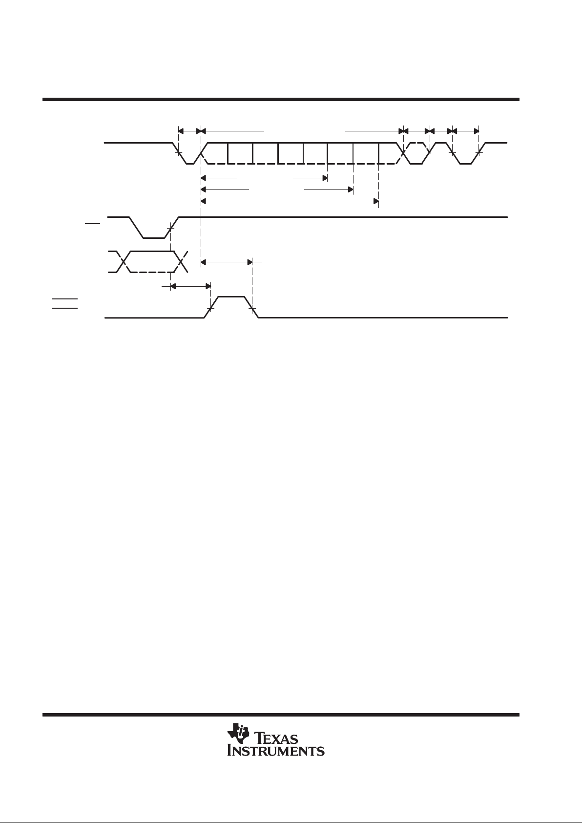
Start
Bit
5 Data Bits
6 Data Bits
7 Data Bits
Parity
Bit
Stop
Bit
Next
Data
Start
Bit
Data Bits (5–8)
T22d
T24d
16 Baud Rate Clock
TX (A–D)
INT (A–D)
IOW
D0 D1 D2 D3 D4 D5 D6 D7
Active
Tx Ready
Active
T23d
Active
Figure 18. Transmit Timing
Start
Bit
Parity
Bit
Stop
Bit
Next
Data
Start
Bit
Data Bits (5–8)
T27d
T28d
TX (A–D)
TXRDY
(A–D)
TXRDY
IOW
D0 D1 D2 D3 D4 D5 D6 D7
Active
Transmitter
Not Ready
Byte 1
Active
Transmitter Ready
D0–D7
Figure 19. Transmit Ready Timing in None FIFO Mode
TL16C754B
QUAD UART WITH 64-BYTE FIFO
SLLS397 – NOVEMBER 1999
24
POST OFFICE BOX 655303 • DALLAS, TEXAS 75265
T27d
T28d
TXRDY
(A–D)
TXRDY
IOW
Active
Trigger
Level
Trigger
Level
D0–D7
Start
Bit
5 Data Bits
6 Data Bits
7 Data Bits
Parity
Bit
Stop
Bit
Data Bits (5–8)
TX (A–D)
D0 D1 D2 D3 D4 D5 D6 D7
Figure 20. Transmit Ready Timing in FIFO Mode
TL16C754B
QUAD UART WITH 64-BYTE FIFO
SLLS397 – NOVEMBER 1999
25
POST OFFICE BOX 655303 • DALLAS, TEXAS 75265
PRINCIPLES OF OPERATION
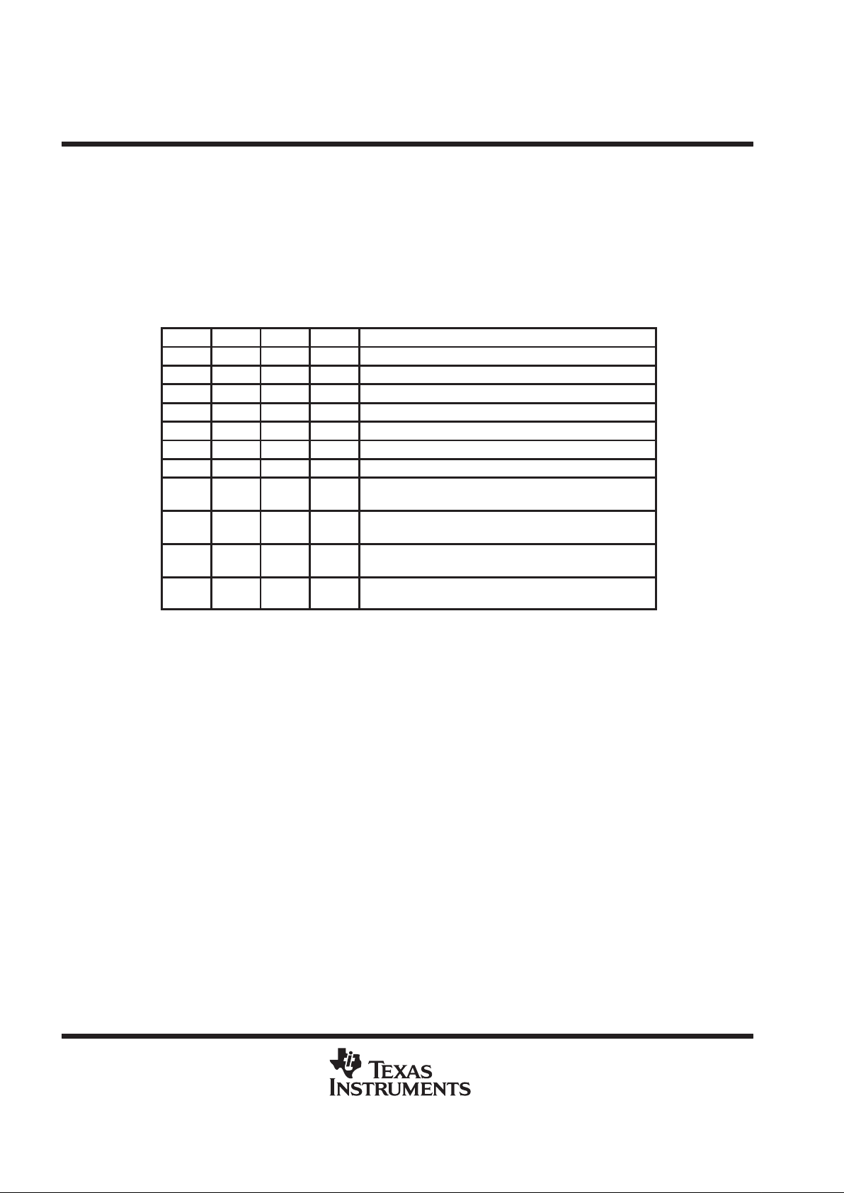
register map
†
Each register is selected using address lines A[0], A[1], A[2] and, in some cases, bits from other registers. The
programming combinations for register selection are shown in Table 7.
Table 7. Register Map – Read/Write Properties
A[2] A[1] A[0] READ MODE WRITE MODE
0 0 0 Receive holding register (RHR) Transmit holding register (THR)
0 0 1 Interrupt enable register (IER) Interrupt enable register
0 1 0 Interrupt identification register (IIR) FIFO control register (FCR)
0 1 1 Line control register (LCR) Line control register
1 0 0 Modem control register (MCR) Modem control register
1 0 1 Line status register (LSR)
1 1 0 Modem status register (MSR)
1 1 1 Scratch register (SPR) Scratch register (SPR)
0 0 0 Divisor latch LSB (DLL) Divisor latch LSB (DLL)
0 0 1 Divisor latch MSB (DLH) Divisor latch MSB (DLH
0 1 0 Enhanced feature register (EFR) Enhanced feature register
1 0 0 Xon-1 word Xon-1 word
1 0 1 Xon-2 word Xon-2 word
1 1 0 Xoff-1 word Xoff-1 word
1 1 1 Xoff-2 word Xoff-2 word
1 1 0 Transmission control register (TCR) Transmission control register
1 1 1 Trigger level register (TLR) Trigger level register
1 1 1 FIFO ready register
†
DLL and DLH are accessible only when LCR bit-7 is 1.
Enhanced feature register , Xon1, 2 and Xoff1, 2 are accessible only when LCR is set to 10111111 (8hBF).
Transmission control register and trigger level register are accessible only when EFR[4] = 1 and MCR[6] = 1, i.e.. EFR[4] and MCR[6] are
read/write enables.
FCR FIFORdy register is accessible when any CS A-D = 0, MCR [2] = 1 and loopback MCR [4] = 0 is disabled.
MCR[7] can only be modified when EFR[4] is set.

TL16C754B
QUAD UART WITH 64-BYTE FIFO
SLLS397 – NOVEMBER 1999
26
POST OFFICE BOX 655303 • DALLAS, TEXAS 75265
PRINCIPLES OF OPERATION
register map (continued)
Table 8 lists and describes the TL16C754B internal registers.
Table 8. TL16C754B Internal Registers
Addr REGISTER BIT 7 BIT 6 BIT 5 BIT 4 BIT 3 BIT 2 BIT 1 BIT 0
READ/
WRITE
000 RHR bit 7 bit 6 bit 5 bit 4 bit 3 bit 2 bit 1 bit 0 Read
000 THR bit 7 bit 6 bit 5 bit 4 bit 3 bit 2 bit 1 bit 0 Write
001 IER 0/CTS
interrupt
enable
†
0/RTS
interrupt
enable
†
0/Xoff
interrupt
enable
†
0/X Sleep
mode
†
Modem
status
interrupt
Rx line
status
interrupt
THR
empty
interrupt
Rx data
available
interrupt
Read/
Write
010 FCR Rx trigger
level
Rx trigger
level
0/TX
trigger
level
†
0/TX
trigger
level
†
DMA
mode
select
Resets
Tx FIFO
Resets
Rx FIFO
Enables
FIFOs
Write
010 IIR FCR(0) FCR(0) 0/CTS,
RTS
†
0/Xoff
†
Interrupt
priority
Bit 2
Interrupt
priority
Bit 1
Interrupt
priority
Bit 0
Interrupt
status
Read
011 LCR DLAB and
EFR
enable
Break
control bit
Sets parity Parity type
select
Parity
enable
No. of stop
bits
Word
length
Word
length
Read/
Write
100 MCR 1x or
4X clock
TCR and
TLR
enable
0/Xon Any 0/Enable
loopback
IRQ
Enable
FIFOrdy
Enable
RTS DTR Read/
Write
101 LSR 0/Error in
Rx FIFO
THR and
TSR
empty
THR
empty
Break
interrupt
Framing
error
Parity
error
Over-run
error
Data in
receiver
Read
110 MSR CD RI DSR CTS ∆CD ∆RI ∆DSR ∆CTS Read
111 SPR bit 7 bit 6 bit 5 bit 4 bit 3 bit 2 bit 1 bit 0 Read/
Write
000 DLL bit 7 bit 6 bit 5 bit 4 bit 3 bit 2 bit 1 bit 0 Read/
Write
001 DLH bit 15 bit 14 bit 13 bit 12 bit 11 bit 10 bit 9 bit 8 Read/
Write
010 EFR Auto-CTS Auto-RTS Special
character
detect
Enable
enhanced-
functions
†
S/W flow
control
Bit 3
S/W flow
control
Bit 2
S/W flow
control
Bit 1
S/W flow
control
Bit 0
Read/
Write
100 Xon1 bit 7 bit 6 bit 5 bit 4 bit 3 bit 2 bit 1 bit 0 Read/
Write
101 Xon2 bit 7 bit 6 bit 5 bit 4 bit 3 bit 2 bit 1 bit 0 Read/
Write
110 Xoff1 bit 7 bit 6 bit 5 bit 4 bit 3 bit 2 bit 1 bit 0 Read/
Write
111 Xoff2 bit 7 bit 6 bit 5 bit 4 bit 3 bit 2 bit 1 bit 0 Read/
Write
110 TCR bit 7 bit 6 bit 5 bit 4 bit 3 bit 2 bit 1 bit 0 Read/
Write
111 TLR bit 7 bit 6 bit 5 bit 4 bit 3 bit 2 bit 1 bit 0 Read/
Write
111 FIFORdy RX FIFO
D status
RX FIFO
C status
RX FIFO
B status
RX FIFO
A status
TX FIFO
D status
TX FIFO
C status
TX FIFO
B status
TX FIFO
A status
Read
†
The shaded bits in the above table can only be modified if EFR[4] is enabled, i.e., if enhanced functions are enabled.
NOTE: Refer to the notes under Table 7 for more register access information.

TL16C754B
QUAD UART WITH 64-BYTE FIFO
SLLS397 – NOVEMBER 1999
27
POST OFFICE BOX 655303 • DALLAS, TEXAS 75265
PRINCIPLES OF OPERATION
receiver holding register (RHR)
The receiver section consists of the receiver holding register (RHR) and the receiver shift register (RSR). The
RHR is actually a 64-byte FIFO. The RSR receives serial data from RX terminal. The data is converted to parallel
data and moved to the RHR. The receiver section is controlled by the line control register. If the FIFO is disabled,
location zero of the FIFO is used to store the characters. If overflow occurs, characters are lost. The RHR also
stores the error status bits associated with each character.
transmit holding register (THR)
The transmitter section consists of the transmit holding register (THR) and the transmit shift register (TSR). The
transmit holding register is actually a 64-byte FIFO. The THR receives data and shifts it into the TSR where it
is converted to serial data and moved out on the TX terminal. If the FIFO is disabled, location zero of the FIFO
is used to store the byte. Characters are lost if overflow occurs.
FIFO control register (FCR)
This is a write-only register which is used for enabling the FIFOs, clearing the FIFOs, setting transmitter and
receiver trigger levels, and selecting the type of DMA signalling. T able 9 shows FIFO control register bit settings.
Table 9. FIFO Control Register (FCR) Bit Settings
BIT NO. BIT SETTINGS
0 0 = Disable the transmit and receive FIFOs
1 = Enable the transmit and receive FIFOs
1 0 = No change
1 = Clears the receive FIFO and resets it’s counter logic to zero. Will return to zero after clearing FIFO.
2 0 = No change
1 = Clears the transmit FIFO and resets it’s counter logic to zero. Will return to zero after clearing FIFO.
3 0 = DMA Mode 0
1 = DMA MOde 1
5:4 Sets the trigger level for the TX FIFO:
00 – 8 spaces
01 – 16 spaces
10 – 32 spaces
11 – 56 spaces
7:6 Sets the trigger level for the RX FIFO:
00 – 8 characters
01 – 16 characters
10 – 56 characters
11 – 60 characters
NOTE: FCR[5–4] can only be modified and enabled when EFR[4] is set. This is because the transmit trigger level is regarded as an enhanced
function.

TL16C754B
QUAD UART WITH 64-BYTE FIFO
SLLS397 – NOVEMBER 1999
28
POST OFFICE BOX 655303 • DALLAS, TEXAS 75265
PRINCIPLES OF OPERATION
line control register (LCR)
This register controls the data communication format. The word length, number of stop bits, and parity type are
selected by writing the appropriate bits to the LCR. Table 10 shows line control register bit settings.
Table 10. Line Control Register (LCR) Bit Settings
BIT NO. BIT SETTINGS
1:0 Specifies the word length to be transmitted or received.
00 – 5 bits
01 – 6 bits
10 – 7 bits
11 – 8 bits
2 Specifies the number of stop bits:
0 – 1 stop bits (Word length = 5, 6, 7, 8)
1 – 1.5 stop bits (Word length = 5)
1 – 2 stop bits (Word length = 6, 7, 8)
3 0 = No parity
1 = A parity bit is generated during transmission and the receiver checks for received parity.
4 0 = Odd parity is generated (if LCR(3) = 1)
1 = Even parity is generated (if LCR(3) = 1)
5 Selects the forced parity format (if LCR(3) = 1)
If LCR(5) = 1 and LCR(4) = 0 the parity bit is forced to 1 in the transmitted and received data.
If LCR(5) = 1 and LCR(4) = 1 the parity bit is forced to 0 in the transmitted and received data.
6 Break control bit.
0 = Normal operating condition
1 = Forces the transmitter output to go low to alert the communication terminal.
7 0 = Normal operating condition
1 = Divisor latch enable
line status register (LSR)
Table 11 shows line status register bit settings.
Table 11. Line Status Register (LSR) Bit Settings
BIT NO. BIT SETTINGS
0 0 = No data in the receive FIFO
1 = At least one character in the RX FIFO
1 0 = No overrun error
1 = Overrun error has occurred.
2 0 = No parity error in data being read from RX FIFO
1 = Parity error in data being read from RX FIFO
3 0 = No framing error in data being read from RX FIFO
1 = Framing error occurred in data being read from RX FIFO (i.e., received data did not have a valid stop bit)
4 0 = No break condition
1 = A break condition occurred and associated byte is 00. (i.e., RX was low for at least one character time frame).
5 0 = Transmit hold register is NOT empty
1 = Transmit hold register is empty. The processor can now load up to 64 bytes of data into the THR if the TX FIFO is enabled.
6 0 = Transmitter hold AND shift registers are not empty.
1 = Transmitter hold AND shift registers are empty .
7 0 = Normal operation
1 = At least one parity error, framing error or break indication are stored in the receiver FIFO. BIt 7 is cleared when no errors are
present in the FIFO.

TL16C754B
QUAD UART WITH 64-BYTE FIFO
SLLS397 – NOVEMBER 1999
29
POST OFFICE BOX 655303 • DALLAS, TEXAS 75265
PRINCIPLES OF OPERATION
line status register (LSR) (continued)
When the LSR is read, LSR[4:2] reflects the error bits [BI, FE, PE] of the character at the top of the RX FIFO
(next character to be read). The LSR[4:2] registers do not physically exist, as the data read from the RX FIFO
is output directly onto the output data-bus, DI[4:2], when the LSR is read. Therefore, errors in a character are
identified by reading the LSR and then reading the RHR.
LSR[7] is set when there is an error anywhere in the RX FIFO and is cleared only when there are no more errors
remaining in the FIFO.
NOTE:
Reading the LSR does not cause an increment of the RX FIFO read pointer. The RX FIFO read
pointer is incremented by reading the RHR.
modem control register (MCR)
The MCR controls the interface with the modem, data set, or peripheral device that is emulating the modem.
Table 12 shows modem control register bit settings.
Table 12. Modem Control Register (MCR) Bit Settings
BIT NO. BIT SETTINGS
0 0 = Force DTR output to inactive (high)
1 = Force DTR
output to active (low).
In loopback controls MSR[5].
1 0 = Force RTS output to inactive (high)
1 = Force RTS
output to active (low).
In loopback controls MSR[4].
If Auto-RTS
is enabled the RTS output is controlled by hardware flow control
2 0 Disables the FIFORdy register
1 Enable the FIFORdy register.
In loopback controls MSR[6].
3 0 = Forces the IRQ(A-D) outputs to high-impedance state
1 = Forces the IRQ(A-D) outputs to the active state.
In loopback controls MSR[7].
4 0 = Normal operating mode
1 = Enable local loopback mode (internal)
In this mode the MCR[3:0] signals are looped back into MSR[3:0] and the TX output is looped back to the RX input internally.
5 0 = Disable Xon Any function
1 = Enable Xon Any function
6 0 = No action
1 = Enable access to the TCR and TLR registers.
7 0 = Divide by one clock input
1 = Divide by four clock input
This bit reflects the inverse of the CLKSEL pin value at the trailing edge of the RESET pulse.
NOTE: MCR[7:5] can only be modified when EFR[4] is set i.e., EFR[4] is a write enable.

TL16C754B
QUAD UART WITH 64-BYTE FIFO
SLLS397 – NOVEMBER 1999
30
POST OFFICE BOX 655303 • DALLAS, TEXAS 75265
PRINCIPLES OF OPERATION
modem status register (MSR)
This 8-bit register provides information about the current state of the control lines from the modem, data set,
or peripheral device to the processor. It also indicates when a control input from the modem changes state.
Table 13 shows modem status register bit settings.
Table 13. Modem Status Register (MSR) Bit Settings
BIT NO. BIT SETTINGS
0 Indicates that CTS input (or MCR[1] in loopback) has changed state. Cleared on a read.
1 Indicates that DSR input (or MCR[0] in loopback) has changed state. Cleared on a read.
2 Indicates that RI input (or MCR[2] in loopback) has changed state from low to high. Cleared on a read.
3 Indicates that CD input (or MCR[3] in loopback) has changed state. Cleared on a read.
4 This bit is equivalent to MCR[1] during local loop-back mode. It is the complement to the CTS input.
5 This bit is equivalent to MCR[0] during local loop-back mode. It is the complement to the DSR input.
6 This bit is equivalent to MCR[2] during local loop-back mode. It is the complement to the RI input.
7 This bit is equivalent to MCR[3] during local loop-back mode. It is the complement to the CD input.
NOTE: The primary inputs RI, CD, CTS, DSR are all active low but their registered equivalents in the MSR and MCR (in loopback) registers are
active high.
interrupt enable register (IER)
The interrupt enable register (IER) enables each of the six types of interrupt, receiver error, RHR interrupt, THR
interrupt, Xoff received, or CTS/RTS change of state from low to high. The INT output signal is activated in
response to interrupt generation. Table 14 shows interrupt enable register bit settings.
Table 14. Interrupt Enable Register (IER) Bit Settings
BIT NO. BIT SETTINGS
0 0 = Disable the RHR interrupt
1 = Enable the RHR interrupt
1 0 = Disable the THR interrupt
1 = Enable the THR interrupt
2 0 = Disable the receiver line status interrupt
1 = Enable the receiver line status interrupt
3 0 = Disable the modem status register interrupt
1 = Enable the modem status register interrupt
4 0 = Disable sleep mode
1 = Enable sleep mode
5 0 = Disable the Xoff interrupt
1 = Enable the Xoff interrupt
6 0 = Disable the RTS interrupt
1 = Enable the RTS
interrupt
7 0 = Disable the CTS interrupt
1 = Enable the CTS
interrupt
NOTE: IER[7:4] can only be modified if EFR[4] is set, i.e., EFR[4] is a write enable.
Re-enabling IER[1] will cause a new interrupt, if the THR is below the threshold.

TL16C754B
QUAD UART WITH 64-BYTE FIFO
SLLS397 – NOVEMBER 1999
31
POST OFFICE BOX 655303 • DALLAS, TEXAS 75265
PRINCIPLES OF OPERATION
interrupt identification register (IIR)
The IIR is a read-only 8-bit register which provides the source of the interrupt in a prioritized manner. Table 15
shows interrupt identification register bit settings.
Table 15. Interrupt Identification Register (IIR) Bit Settings
BIT NO. BIT SETTINGS
0 0 = An interrupt is pending
1 = No interrupt is pending
3:1 3-Bit encoded interrupt. See Table 14.
4 1 = Xoff/Special character has been detected.
5 CTS/RTS low to high change of state
7:6 Mirror the contents of FCR[0]
The interrupt priority list is illustrated in Table 16.
Table 16. Interrupt Priority List
PRIORITY
LEVEL
BIT 5 BIT 4 BIT 3 BIT 2 BIT 1 BIT 0 INTERRUPT SOURCE
1 0 0 0 1 1 0 Receiver line status error
2 0 0 1 1 0 0 Receiver timeout interrupt
2 0 0 0 1 0 0 RHR interrupt
3 0 0 0 0 1 0 THR interrupt
4 0 0 0 0 0 0 Modem interrupt
5 0 1 0 0 0 0 Received Xoff signal/special character
6 1 0 0 0 0 0 CTS, RTS change of state from active (low) to inactive (high)
enhanced feature register (EFR)
This 8-bit register enables or disables the enhanced features of the UART . T able 17 shows the enhanced feature
register bit settings.
Table 17. Enhanced Feature Register (EFR) Bit Settings
BIT NO. BIT SETTINGS
3:0 Combinations of software flow control can be selected by programming bit 3–bit 0. See Table 1.
4 Enhanced functions enable bit.
0 = Disables enhanced functions and writing to IER bits 4–7, FCR bits 4–5, MCR bits 5–7.
1 =Enables the enhanced function IER bits 4–7, FCR bit 4–5, and MCR bits 5–7 can be modified, i.e., this bit is therefore a
write enable.
5 0 = Normal operation
1 = Special character detect. Received data is compared with Xoff-2 data. If a match occurs, the received data is transferred to
FIFO and IIR bit 4 is set to 1 to indicate a special character has been detected.
6 RTS flow control enable bit
0 = Normal operation
1 = RTS
flow control is enabled i.e., RTS pin goes high when the receiver FIFO HALT trigger level TCR[3:0] is reached, and
goes low when the receiver FIFO RESTORE transmission trigger level TCR[7:4] is reached.
7 CTS flow control enable bit
0 = Normal operation
1 = CTS
flow control is enabled i.e., transmission is halted when a high signal is detected on the CTS pin.

TL16C754B
QUAD UART WITH 64-BYTE FIFO
SLLS397 – NOVEMBER 1999
32
POST OFFICE BOX 655303 • DALLAS, TEXAS 75265
PRINCIPLES OF OPERATION
divisor latches (DLL, DLH)
Two 8-bit registers store the 16-bit divisor for generation of the baud clock in the baud rate generator. DLH,
stores the most significant part of the divisor. DLL stores the least significant part of the division.
DLL and DLH can only be written to before sleep mode is enabled (i.e., before IER[4] is set).
transmission control register (TCR)
This 8-bit register is used to store the receive FIFO threshold levels to start/stop transmission during
hardware/software flow control. Table 18 shows transmission control register bit settings.
Table 18. Transmission Control Register (TCR) Bit Settings
BIT NO. BIT SETTINGS
3:0 RCV FIFO trigger level to HALT transmission (0–60)
7:4 RCV FIFO trigger level to RESTORE transmission (0–60)
TCR trigger levels are available from 0–60 bytes with a granularity of four.
TCR can only be written to when EFR[4] = 1 and MCR[6] = 1. The programmer must program the TCR such
that TCR[3:0] > TCR[7:4]. There is no built-in hardware check to make sure this condition is met. Also, the TCR
must be programmed with this condition before Auto-RTS or software flow control is enabled to avoid spurious
operation of the device.
trigger level register (TLR)
This 8-bit register is used to store the transmit and received FIFO trigger levels used for DMA and interrupt
generation. Trigger levels from 4–60 can be programmed with a granularity of 4. Table 19 shows trigger level
register bit settings.
Table 19. Trigger Level Register (TLR) Bit Settings
BIT NO. BIT SETTINGS
3:0 Transmit FIFO trigger levels (4–60), number of spaces available
7:4 RCV FIFO trigger levels (4–60), number of characters available
TLR can only be written to when EFR[4] = 1 and MCR[6] = 1. If TLR[3:0] or TLR[7:4] are zero, then the selectable
trigger levels via the FIFO control register (FCR) are used for the transmit and receive FIFO trigger levels.
Trigger levels from 4–60 bytes are available with a granularity of four . The TLR should be programmed for N/4,
where N is the desired trigger level.
FIFO ready register
The FIFO ready register provides real-time status of the transmit and receive FIFOs. T able 20 shows the FIFO
ready register bit settings.
Table 20. FIFO Ready Register
BIT NO. BIT SETTINGS
3:0 0 = There are less than a TX trigger level number of spaces available in the TX FIFO.
1 = There are at least a TX trigger level number of spaces available in the TX FIFO
7:4 0 = There are less than a RX trigger level number of characters in the RX FIFO.
1 = The RX FIFO has more than a RX trigger level number of characters available for reading OR a timeout condition has occurred.
The FIFORdy register is a read only register and can be accessed when any of the four UARTs are selected
CAS A-D = 0, MCR[2] (FIFORdy Enable) is a 1 and loopback is disabled. Its address space is 111.

TL16C754B
QUAD UART WITH 64-BYTE FIFO
SLLS397 – NOVEMBER 1999
33
POST OFFICE BOX 655303 • DALLAS, TEXAS 75265
PRINCIPLES OF OPERATION
TL16C754B Programmer’s Guide
The base set of registers that are used during high speed data transfer have a straightforward access method.
The extended function registers require special access bits to be decoded along with the address lines. The
following guide will help with programming these registers. Note that the descriptions below are for individual
register access. Some streamlining through interleaving can be obtained when programming all the registers.
Set baud rate to VALUE1,VALUE2 Read LCR (03), save in temp
Set LCR (03) to 80
Set DLL (00) to VALUE1
Set DLM (01) to VALUE2
Set LCR (03) to temp
Set Xoff1,Xon1 to VALUE1,VALUE2 Read LCR (03), save in temp
Set LCR (03) to BF
Set Xoff1 (06) to VALUE1
Set Xon1 (04) to VALUE2
Set LCR (03) to temp
Set Xoff2,Xon2 to VALUE1,VALUE2 Read LCR (03), save in temp
Set LCR (03) to BF
Set Xoff2 (07) to VALUE1
Set Xon2 (05) to VALUE2
Set LCR (03) to temp
Set software flow control mode to VALUE Read LCR (03), save in temp
Set LCR (03) to BF
Set EFR (02) to VALUE
Set LCR (03) to temp
Set flow control threshold to VALUE Read LCR (03), save in temp1
Set LCR (03) to BF
Read EFR (02), save in temp2
Set EFR (02) to 10 + temp2
Set LCR (03) to 00
Read MCR (04), save in temp3
Set MCR (04) to 40 + temp3
Set TCR (06) to VALUE
Set LCR (03) to BF
Set EFR (02) to temp2
Set LCR (03) to temp1
Set MCR (04) to temp3

TL16C754B
QUAD UART WITH 64-BYTE FIFO
SLLS397 – NOVEMBER 1999
34
POST OFFICE BOX 655303 • DALLAS, TEXAS 75265
Set xmt and rcv FIFO thresholds to VALUE Read LCR (03), save in temp1
Set LCR (03) to BF
Read EFR (02), save in temp2
Set EFR (02) to 10 + temp2
Set LCR (03) to 00
Read MCR (04), save in temp3
Set MCR (04) to 40 + temp3
Set TLR (07) to VALUE
Set LCR (03) to BF
Set EFR (02) to temp2
Set LCR (03) to temp1
Set MCR (04) to temp3
Read FIFORdy register Read MCR (04), save in temp1
Set temp2 = temp1 * EF
Set MCR (04), save in temp2
Read FRR (07), save in temp2
Pass temp2 back to host
Set MCR (04) to temp1

TL16C754B
QUAD UART WITH 64-BYTE FIFO
SLLS397 – NOVEMBER 1999
35
POST OFFICE BOX 655303 • DALLAS, TEXAS 75265
MECHANICAL DATA
FN (S-PQCC-J**) PLASTIC J-LEADED CHIP CARRIER
4040005/B 03/95
20 PIN SHOWN
0.026 (0,66)
0.032 (0,81)
D2/E2
0.020 (0,51) MIN
0.180 (4,57) MAX
0.120 (3,05)
0.090 (2,29)
D2/E2
0.013 (0,33)
0.021 (0,53)
Seating Plane
MAX
D2/E2
0.219 (5,56)
0.169 (4,29)
0.319 (8,10)
0.469 (11,91)
0.569 (14,45)
0.369 (9,37)
MAX
0.356 (9,04)
0.456 (11,58)
0.656 (16,66)
0.008 (0,20) NOM
1.158 (29,41)
0.958 (24,33)
0.756 (19,20)
0.191 (4,85)
0.141 (3,58)
MIN
0.441 (11,20)
0.541 (13,74)
0.291 (7,39)
0.341 (8,66)
18
19
14
13
D
D1
13
9
E1E
4
8
MINMAXMIN
PINS
**
20
28
44
0.385 (9,78)
0.485 (12,32)
0.685 (17,40)
52
68
84
1.185 (30,10)
0.985 (25,02)
0.785 (19,94)
D/E
0.395 (10,03)
0.495 (12,57)
1.195 (30,35)
0.995 (25,27)
0.695 (17,65)
0.795 (20,19)
NO. OF
D1/E1
0.350 (8,89)
0.450 (11,43)
1.150 (29,21)
0.950 (24,13)
0.650 (16,51)
0.750 (19,05)
0.004 (0,10)
M
0.007 (0,18)
0.050 (1,27)
NOTES: A. All linear dimensions are in inches (millimeters).
B. This drawing is subject to change without notice.
C. Falls within JEDEC MS-018
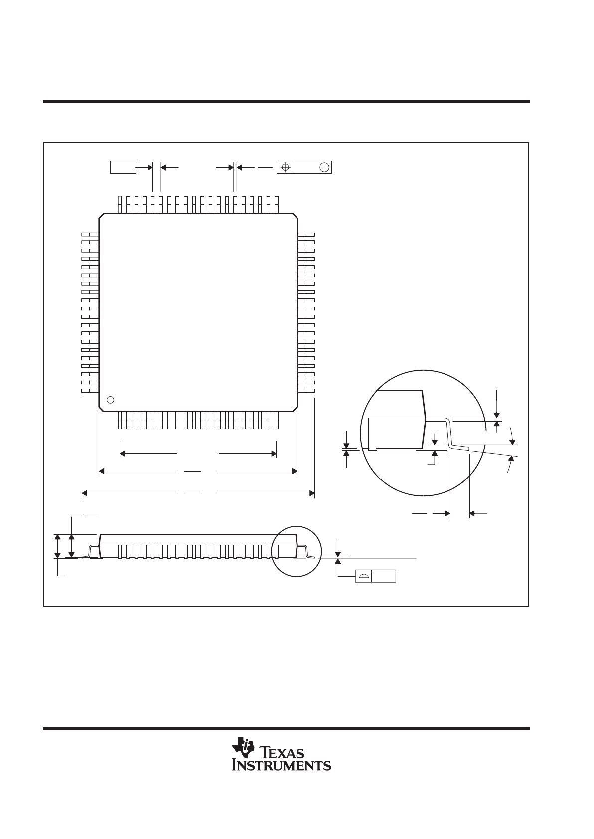
TL16C754B
QUAD UART WITH 64-BYTE FIFO
SLLS397 – NOVEMBER 1999
36
POST OFFICE BOX 655303 • DALLAS, TEXAS 75265
MECHANICAL DATA
PN (S-PQFP-G80) PLASTIC QUAD FLATPACK
4040135 / B 11/96
0,17
0,27
0,13 NOM
40
21
0,25
0,45
0,75
0,05 MIN
Seating Plane
Gage Plane
41
60
61
80
20
SQ
SQ
1
13,80
14,20
12,20
9,50 TYP
11,80
1,45
1,35
1,60 MAX
0,08
0,50
M
0,08
0°–7°
NOTES: A. All linear dimensions are in millimeters.
B. This drawing is subject to change without notice.
C. Falls within JEDEC MS-026

IMPORTANT NOTICE
T exas Instruments and its subsidiaries (TI) reserve the right to make changes to their products or to discontinue
any product or service without notice, and advise customers to obtain the latest version of relevant information
to verify, before placing orders, that information being relied on is current and complete. All products are sold
subject to the terms and conditions of sale supplied at the time of order acknowledgement, including those
pertaining to warranty, patent infringement, and limitation of liability.
TI warrants performance of its semiconductor products to the specifications applicable at the time of sale in
accordance with TI’s standard warranty. Testing and other quality control techniques are utilized to the extent
TI deems necessary to support this warranty. Specific testing of all parameters of each device is not necessarily
performed, except those mandated by government requirements.
CERT AIN APPLICATIONS USING SEMICONDUCTOR PRODUCTS MAY INVOLVE POTENTIAL RISKS OF
DEATH, PERSONAL INJURY, OR SEVERE PROPERTY OR ENVIRONMENTAL DAMAGE (“CRITICAL
APPLICATIONS”). TI SEMICONDUCTOR PRODUCTS ARE NOT DESIGNED, AUTHORIZED, OR
WARRANTED TO BE SUITABLE FOR USE IN LIFE-SUPPORT DEVICES OR SYSTEMS OR OTHER
CRITICAL APPLICATIONS. INCLUSION OF TI PRODUCTS IN SUCH APPLICA TIONS IS UNDERSTOOD T O
BE FULLY AT THE CUSTOMER’S RISK.
In order to minimize risks associated with the customer’s applications, adequate design and operating
safeguards must be provided by the customer to minimize inherent or procedural hazards.
TI assumes no liability for applications assistance or customer product design. TI does not warrant or represent
that any license, either express or implied, is granted under any patent right, copyright, mask work right, or other
intellectual property right of TI covering or relating to any combination, machine, or process in which such
semiconductor products or services might be or are used. TI’s publication of information regarding any third
party’s products or services does not constitute TI’s approval, warranty or endorsement thereof.
Copyright 1999, Texas Instruments Incorporated
 Loading...