


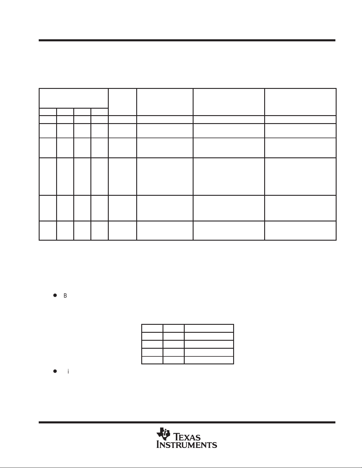
D
Pin-to-Pin Compatible With the Existing
TL16C550B/C
D
Programmable 16- or 64-Byte FIFOs to
Reduce CPU Interrupts
D
Programmable Auto-RTS and Auto-CTS
D
In Auto-CTS Mode, CTS Controls
Transmitter
D
In Auto-RTS Mode, Receiver FIFO Contents
and Threshold Control RTS
D
Serial and Modem Control Outputs Drive a
RJ11 Cable Directly When Equipment Is on
the Same Power Drop
D
Capable of Running With All Existing
TL16C450 Software
D
After Reset, All Registers Are Identical to
the TL16C450 Register Set
D
Up to 16-MHz Clock Rate for Up to 1-Mbaud
Operation
D
In the TL16C450 Mode, Hold and Shift
Registers Eliminate the Need for Precise
Synchronization Between the CPU and
Serial Data
D
Programmable Baud Rate Generator Allows
Division of Any Input Reference Clock by 1
16
to (2
Clock
D
Standard Asynchronous Communication
Bits (Start, Stop, and Parity) Added or
Deleted to or From the Serial Data Stream
D
5-V and 3-V Operation
–1) and Generates an Internal 16 ×
description
TL16C750
ASYNCHRONOUS COMMUNICATIONS ELEMENT
WITH 64-BYTE FIFOs AND AUTOFLOW CONTROL
SLLS191C – JANUARY 1995 – REVISED DECEMBER 1997
D
Register Selectable Sleep Mode and
Low-Power Mode
D
Independent Receiver Clock Input
D
Independently Controlled Transmit,
Receive, Line Status, and Data Set
Interrupts
D
Fully Programmable Serial Interface
Characteristics:
– 5-, 6-, 7-, or 8-Bit Characters
– Even-, Odd-, or No-Parity Bit Generation
and Detection
– 1-, 1 1/2-, or 2-Stop Bit Generation
– Baud Generation (DC to 1 Mbits Per
Second)
D
False Start Bit Detection
D
Complete Status Reporting Capabilities
D
3-State Output CMOS Drive Capabilities for
Bidirectional Data Bus and Control Bus
D
Line Break Generation and Detection
D
Internal Diagnostic Capabilities:
– Loopback Controls for Communications
Link Fault Isolation
– Break, Parity, Overrun, Framing Error
Simulation
D
Fully Prioritized Interrupt System Controls
D
Modem Control Functions (CTS, RTS, DSR,
DTR
, RI, and DCD)
D
Available in 44-Pin PLCC and 64-Pin SQFP
D
Industrial T emperature Range Available for
64-Pin SQFP
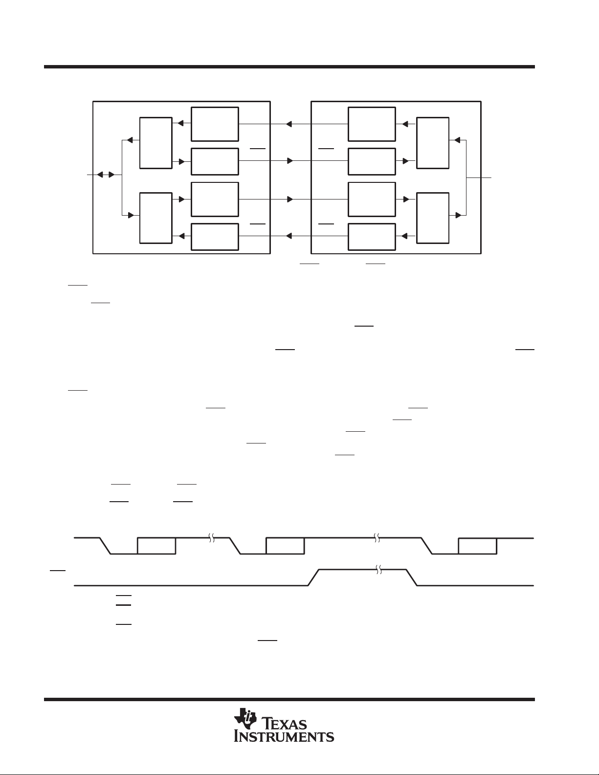
The TL16C750 is a functional upgrade of the TL16C550C asynchronous communications element (ACE),
which in turn is a functional upgrade of the TL16C450. Functionally equivalent to the TL16C450 on power up
(character or TL16C450 mode), the TL16C750, like the TL16C550C, can be placed in an alternate mode (FIFO
mode). This relieves the CPU of excessive software overhead by buffering received and transmitted characters.
The receiver and transmitter FIFOs store up to 64 bytes including three additional bits of error status per byte
for the receiver FIFO. The user can choose between a 16-byte FIFO mode or an extended 64-byte FIFO mode.
In the FIFO mode, there is a selectable autoflow control feature that can significantly reduce software overload
and increase system efficiency by automatically controlling serial data flow through the RTS
input signals (see Figure 1).
The TL16C750 performs serial-to-parallel conversion on data received from a peripheral device or modem and
parallel-to-serial conversion on data received from its CPU. The CPU can read the ACE status at any time. The
ACE includes complete modem control capability and a processor interrupt system that can be tailored to
minimize software management of the communications link.
Please be aware that an important notice concerning availability, standard warranty, and use in critical applications of
Texas Instruments semiconductor products and disclaimers thereto appears at the end of this data sheet.
PRODUCTION DATA information is current as of publication date.
Products conform to specifications per the terms of Texas Instruments
standard warranty. Production processing does not necessarily include
testing of all parameters.
POST OFFICE BOX 655303 • DALLAS, TEXAS 75265
Copyright 1997, Texas Instruments Incorporated
output and the CTS
1
TL16C750
ASYNCHRONOUS COMMUNICATIONS ELEMENT
WITH 64-BYTE FIFOs AND AUTOFLOW CONTROL
SLLS191C – JANUARY 1995 – REVISED DECEMBER 1997
description (continued)
The TL16C750 ACE includes a programmable baud rate generator capable of dividing a reference clock by
16
divisors from 1 to (2
– 1) and producing a 16× reference clock for the internal transmitter logic. Provisions are
also included to use this 16 × clock for the receiver logic. The ACE accommodates a 1-Mbaud serial rate
(16-MHz input clock) so a bit time is 1 µs and a typical character time is 10 µs (start bit, 8 data bits, stop bit).
Two of the TL16C450 terminal functions have been changed to TXRDY
and RXRDY, which provide signaling
to a direct memory access (DMA) controller.
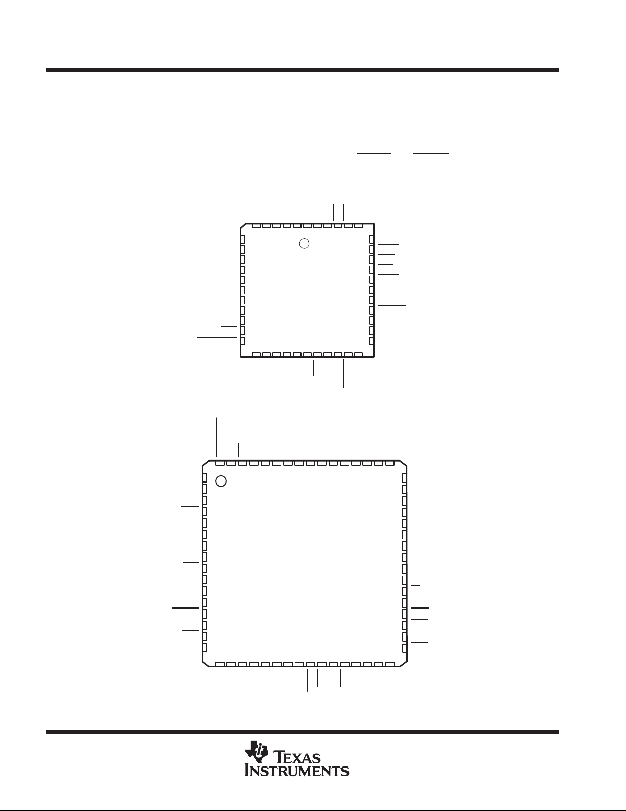
FN PACKAGE
(TOP VIEW)
CC
RI
DCD
DSR
D5
D6
D7
RCLK
SIN
NC
SOUT
CS0
CS1
CS2
BAUDOUT
D4D3D2D1D0NCV
543216
7
8
9
10
11
12
13
14
15
16
17
20 21 22 23
18 19
XIN
WR1
WR2
XOUT
PM PACKAGE
(TOP VIEW)
44
24 25 26 2728
SS
NC
V
RD1
RD2
42 41 4043
DDIS
CTS
39
38
37
36
35
34
33
32
31
30
29
ADS
TXRDY
MR
OUT1
DTR
RTS
OUT2
NC
INTRPT
RXRDY
A0
A1
A2
BAUDOUT
NC
CS2NCCS1NCCS0
XIN
XOUT
NC
WR1
NC
WR2
NC
V
SS
RD1
RD2
NC
DDIS
TXRDY
NC
ADS
NC
63 62 61 60 5964 58
1
2
3
4
5
6
7
8
9
10
11
12
13
14
15
16
18 19
17
A2
A1
NC
20
A0
NC–No internal connection
SOUT
21 22 23 24
NC
RXRDY
INTRPT
RCLK
SIN
NC
56 55 5457
25 26 27 28 29
NC
RTS
OUT2
NC
NC
53 52
DTR
D7NCD5
D6
51 50 49
30 31 32
NC
NC
OUT1
48
47
46
45
44
43
42
41
40
39
38
37
36
35
34
33
MR
D4
NC
D3
D2
NC
D1
D0
NC
V
CC
NC
RI
NC
DCD
DSR
NC
CTS
2
POST OFFICE BOX 655303 • DALLAS, TEXAS 75265
functional block diagram
8
Data
Bus
Buffer
Select
and
Control
Logic
Power
Supply
D(7–0)
CS0
CS1
CS2
ADS
MR
RD1
RD2
WR1
WR2
DDIS
TXRDY
XIN
XOUT
RXRDY
V
CC
V
SS
A0
A1
A2
9–2
44
22
31
30
29
14
15
16
28
39
24
25
20
21
26
27
18
19
32
Internal
Data Bus
S
e
l
e
c
t
8
Receiver
Buffer
Register
Line
Control
Register
Divisor
Latch (LS)
Divisor
Latch (MS)
Line
Status
Register
Transmitter
Holding
Register
Modem
Control
Register
Modem
Status
Register
Interrupt
Enable
Register
TL16C750
ASYNCHRONOUS COMMUNICATIONS ELEMENT
WITH 64-BYTE FIFOs AND AUTOFLOW CONTROL
SLLS191C – JANUARY 1995 – REVISED DECEMBER 1997
Receiver
FIFO
Generator
Transmitter
FIFO
Interrupt
8
Control
Logic
Baud
S
e
l
e
8 8
c
t
8
8
Receiver
Shift
Register
Receiver
Timing and
Control
Transmitter
Timing and
Control
Transmitter
Shift
Register
Modem
Control
Logic
11
SIN
10
RCLK
36
17
BAUDOUT
Autoflow
Control
Enable
(AFE)
13
40
CTS
37
DTR
41
DSR
42
DCD
43
RI
38
OUT1
35
OUT2
33
INTRPT
RTS
SOUT
Interrupt
Identification
Register
FIFO
Control
Register
NOTE A: Terminal numbers shown are for the FN package.
POST OFFICE BOX 655303 • DALLAS, TEXAS 75265
8
3
TL16C750
ASYNCHRONOUS COMMUNICATIONS ELEMENT
WITH 64-BYTE FIFOs AND AUTOFLOW CONTROL
SLLS191C – JANUARY 1995 – REVISED DECEMBER 1997
Terminal Functions
TERMINAL
NAME
A0
A1
A2
ADS 28 15 I Address strobe. When ADS is active (low), the register select signals (A0, A1, and A2) and chip select signals
BAUDOUT 17 64 O Baud out. BAUDOUT is a 16× clock signal for the transmitter section of the ACE. The clock rate is established
CS0
CS1
CS2
CTS 40 33 I Clear to send. CTS is a modem status signal. Its condition can be checked by reading bit 4 (CTS) of the
D0
D1
D2
D3
D4
D5
D6
D7
DCD 42 36 I Data carrier detect. DCD is a modem status signal. Its condition can be checked by reading bit 7 (DCD) of
DDIS 26 12 O Driver disable. DDIS is active (high) when the CPU is not reading data. When active, DDIS can disable an
DSR 41 35 I Data set ready. DSR is a modem status signal. Its condition can be checked by reading bit 5 (DSR) of the
DTR 37 28 O Data terminal ready . When active (low), DTR informs a modem or data set that the ACE is ready to establish
INTRPT 33 23 O Interrupt. When active (high), INTRPT informs the CPU that the ACE has an interrupt to be serviced. Four
MR 39 32 I Master reset. When active (high), MR clears most ACE registers and sets the levels of various output signals
OUT1
OUT2
RCLK 10 54 I Receiver clock. RCLK is the 16× baud rate clock for the receiver section of the ACE.
NO.FNNO.
31
30
29
14
15
16
2
3
4
5
6
7
8
9
38353025O Outputs 1 and 2. These are user-designated output terminals that are set to their active (low) level by setting
I/O
PM
20
I Register select. A0–A2 are used during read and write operations to select the ACE register to read from
18
17
59
61
62
42
43
45
46
48
50
51
52
or write to. Refer to Table 1 for register addresses and ADS
(CS0, CS1, CS2
signals are held at the logic levels they were in when the low-to-high transition of ADS
by the reference oscillator frequency divided by a divisor specified by the baud generator divisor latches.
BAUDOUT
I Chip select. When CS0 and CS1 are high and CS2 is low, the ACE is selected. When any of these inputs
are inactive, the ACE remains inactive. Refer to the ADS
modem status register. Bit 0 (∆CTS) of the modem status register indicates that CTS
since the last read from the modem status register. When the modem status interrupt is enabled, CTS
changes states, and the auto-CTS mode is not enabled, an interrupt is generated. CTS is also used in the
auto-CTS
I/O Data bus. Eight data lines with 3-state outputs provide a bidirectional path for data, control, and status
information between the ACE and the CPU. As inputs, they use fail safe CMOS compatible input buffers.
the modem status register. Bit 3 (∆DCD) of the modem status register indicates that DCD
since the last read from the modem status register. When the modem status interrupt is enabled and DCD
changes state, an interrupt is generated.
external transceiver.
modem status register. Bit 1 (∆DSR) of the modem status register indicates DSR
the last read from the modem status register. When the modem status interrupt is enabled and the DSR
changes states, an interrupt is generated.
communication. DTR
DTR
is placed in the inactive condition either as a result of a master reset, during loop mode operation, or
clearing the DTR bit.
conditions that cause an interrupt to be issued are: a receiver error, received data that is available or timed
out (FIFO mode only), an empty transmitter holding register, or an enabled modem status interrupt. INTRPT
is reset (deactivated) either when the interrupt is serviced or as a result of a master reset.
(refer to Table 2).
their respective modem control register (MCR) bits (OUT1 and OUT2). OUT1
inactive (high) level as a result of master reset, during loop mode operations, or by clearing bit 2 (OUT1) or
bit 3 (OUT2) of the MCR.
) drive the internal select logic directly; when ADS is high, the register select and chip select
can also be used for the receiver section by tying this output to RCLK.
mode to control the transmitter.
is placed in the active state by setting the DTR bit of the modem control register to one.
DESCRIPTION
signal description.
occurred.
signal description.
has changed states
has changed states
has changed states since
and OUT2 are set to their
4
POST OFFICE BOX 655303 • DALLAS, TEXAS 75265
TL16C750
ASYNCHRONOUS COMMUNICATIONS ELEMENT
WITH 64-BYTE FIFOs AND AUTOFLOW CONTROL
SLLS191C – JANUARY 1995 – REVISED DECEMBER 1997
Terminal Functions (Continued)
TERMINAL
PM
I/O
Read inputs. When either RD1 or RD2 is active (low or high respectively) while the ACE is selected, the CPU
is allowed to read status information or data from a selected ACE register. Only one of these inputs is required
for the transfer of data during a read operation; the other input should be tied in its inactive state (i.e., RD2 tied
low or RD1
status register. Bit 2 (TERI) of the modem status register indicates that RI
level since the last read from the modem status register. If the modem status interrupt is enabled when this
transition occurs, an interrupt is generated.
is set to its active level by setting the RTS MCR bit and is set to its inactive (high) level either as a result of a
master reset, during loop mode operations, or by clearing bit 1 (RTS) of the MCR. In the auto-RTS
is set to its inactive level by the receiver threshold control logic.
in the FIFO mode, one of two types of DMA signalling can be selected through the FIFO control register bit
3 (FCR3). When operating in the TL16C450 mode, only DMA mode 0 is allowed. Mode 0 supports
single-transfer DMA in which a transfer is made between CPU bus cycles. Mode 1 supports multitransfer DMA
in which multiple transfers are made continuously until the receiver FIFO has been emptied. In DMA mode 0
(FCR0 = 0 or FCR0 = 1, FCR3 = 0), when there is at least one character in the receiver FIFO or receiver holding
register, RXRDY
holding register, RXRDY
or the timeout has been reached, RXRDY
characters in the FIFO or holding register, it goes inactive (high).
as a result of master reset.
one of two types of DMA signalling can be selected through FCR3. When operating in the TL16C450 mode,
only DMA mode 0 is allowed. Mode 0 supports single-transfer DMA in which a transfer is made between CPU
bus cycles. Mode 1 supports multitransfer DMA in which multiple transfers are made continuously until the
transmit FIFO has been filled.
allowed to write control words or data into a selected ACE register. Only one of these inputs is required to
transfer data during a write operation; the other input should be tied in its inactive state (i.e., WR2 tied low or
WR1
tied high).
is active (low). When RXRDY has been active but there are no characters in the FIFO or
goes inactive (high). In DMA mode 1 (FCR0 = 1, FCR3 = 1), when the trigger level
tied high).
NAME
RD1
RD2
RI 43 38 I Ring indicator. RI is a modem status signal. Its condition can be checked by reading bit 6 (RI) of the modem
RTS 36 26 O Request to send. When active, RTS informs the modem or data set that the ACE is ready to receive data. RTS
RXRDY 32 21 O Receiver ready. Receiver direct memory access (DMA) signalling is available with RXRDY. When operating
SIN 11 55 I Serial data. SIN is the input from a connected communications device.
SOUT 13 58 O Composite serial data output to a connected communication device. SOUT is set to the marking (high) level
TXRDY 27 13 O Transmitter ready. Transmitter DMA signalling is available with TXRDY. When operating in the FIFO mode,
V
CC
V
SS
WR1
WR2
XIN
XOUT
NO.FNNO.
2425910I
44 40 5-V supply voltage
22 8 Supply common
202146I Write inputs. When either input is active (low or high respectively) and while the ACE is selected, the CPU is
181912I/O External clock. XIN and XOUT connect the ACE to the main timing reference (clock or crystal).
DESCRIPTION
has transitioned from a low to a high
mode, RTS
goes active (low); when it has been active but there are no more
detailed description
autoflow control
Auto-flow control is composed of auto-CTS
transmit FIFO can emit data (see Figure 1). With auto-RTS
or the threshold has not been reached. When RTS
unless the receive FIFO has empty space. Thus, overrun errors are eliminated when ACE1 and ACE2 are
TLC16C750s with enabled autoflow control. If not, overrun errors occur if the transmit data rate exceeds the
receive FIFO read latency.
POST OFFICE BOX 655303 • DALLAS, TEXAS 75265
and auto-RTS. With auto-CTS, CTS must be active before the
, RTS becomes active when the receiver is empty
is connected to CTS, data transmission does not occur
5
TL16C750
ASYNCHRONOUS COMMUNICATIONS ELEMENT
WITH 64-BYTE FIFOs AND AUTOFLOW CONTROL
SLLS191C – JANUARY 1995 – REVISED DECEMBER 1997
autoflow control (continued)
ACE1 ACE2
Serial to
Parallel
RCV
FIFO
Flow
Control
D7–D0
Parallel
to Serial
XMT
FIFO
Flow
Control
SIN SOUT
RTS
SOUT SIN
CTS
CTS
RTS
Parallel
to Serial
XMT
FIFO
Flow
Control
Serial to
Parallel
RCV
FIFO
Flow
Control
Figure 1. Autoflow Control (auto-RTS and auto-CTS) Example
auto-RTS (see Figure 1)
Auto-RTS
data flow control originates in the receiver timing and control block (see functional block diagram)
and is linked to the programmed receiver FIFO trigger level. When the receiver FIFO level reaches a trigger level
of 1, 4, 8, or 14 in 16-byte mode or 1, 16, 32, or 56 in 64-byte mode, RTS
is deasserted. The sending ACE may
send an additional byte after the trigger level is reached (assuming the sending ACE has another byte to send)
because it may not recognize the deassertion of RTS
until after it has begun sending the additional byte. RTS
is automatically reasserted once the receiver FIFO is emptied by reading the receiver buffer register. The
reassertion signals the sending ACE to continue transmitting data.
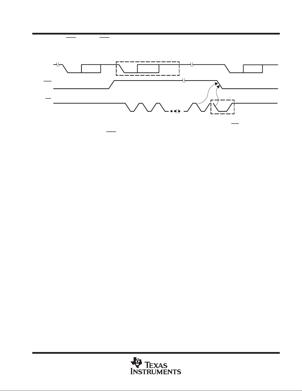
auto-CTS
(see Figure 1)
D7–D0
The transmitter circuitry checks CTS
sends the next byte. To stop the transmitter from sending the following byte, CTS
middle of the last stop bit that is currently being sent. The auto-CTS
system. When flow control is enabled, the CTS
device automatically controls its own transmitter. Without auto-CTS
before sending the next data byte. When CTS is active, the transmitter
must be released before the
function reduces interrupts to the host
state changes and does not trigger host interrupts because the
, the transmitter sends any data present in
the transmit FIFO and a receiver overrun error can result.
enabling auto-RTS
and auto-CTS
The auto-RTS and auto-CTS modes of operation are activated by setting bit 5 of the modem control register
(MCR) to 1 (see Figure 2).
SOUT
CTS
NOTES: A. When CTS is low, the transmitter keeps sending serial data out.
B. When CTS
C. When CTS
Start Bits 0–7 Start Bits 0–7 Start Bits 0–7
goes high before the middle of the last stop bit of the current byte, the transmitter finishes sending the current byte but
it does not send the next byte.
goes from high to low, the transmitter begins sending data again.
Stop Stop Stop
Figure 2. CTS Functional Timing
6
POST OFFICE BOX 655303 • DALLAS, TEXAS 75265
ASYNCHRONOUS COMMUNICATIONS ELEMENT
WITH 64-BYTE FIFOs AND AUTOFLOW CONTROL
SLLS191C – JANUARY 1995 – REVISED DECEMBER 1997
enabling auto-RTS and auto-CTS (continued)
The receiver FIFO trigger level can be set to 1, 4, 8, or 14 bytes for the 16-byte mode and 1, 16, 32, or 56 bytes
for 64-byte mode (see Figure 3).
TL16C750
SIN
RTS
RD
(RD RBR)
NOTES: A. N = receiver FIFO trigger level
B. The two blocks in dashed lines cover the case where an additional byte is sent as described in auto-RTS
Start Byte N Start Byte N+1 Start Byte
Stop Stop Stop
12
N N+1
.
Figure 3. RTS Functional Timing, Receiver FIFO Trigger Level
absolute maximum ratings over operating free-air temperature range (unless otherwise noted)
(see Note 1) –0.5 V to 6 V. . . . . . . . . . . . . . . . . . . . . . . . . . . . . . . . . . . . . . . . . . . . . .
Supply voltage range, V
Input voltage range, V
Output voltage range, V
Input clamp current, I
Output clamp current, I
Operating free-air temperature range, T
Operating free-air temperature range, T
Storage temperature range, T
†
Stresses beyond those listed under “absolute maximum ratings” may cause permanent damage to the device. These are stress ratings only, and
functional operation of the device at these or any other conditions beyond those indicated under “recommended operating conditions” is not
implied. Exposure to absolute-maximum-rated conditions for extended periods may affect device reliability.
NOTES: 1. This applies for external input and bidirectional buffers. VI > VCC does not apply to fail safe terminals.
2. This applies for external output and bidirectional buffers. VO > VCC does not apply to fail safe terminals.
CC
: Standard –0.5 V to V
I
Fail safe –0.5 V to 6.5 V. . . . . . . . . . . . . . . . . . . . . . . . . . . . . . . . . . . . . . . . . . . . . . . . . . .
: Standard –0.5 V to V
O
Fail safe –0.5 V to 6.5 V. . . . . . . . . . . . . . . . . . . . . . . . . . . . . . . . . . . . . . . . . . . . . . . . .
(VI < 0 or VI > VCC) (see Note 1) ±20 mA. . . . . . . . . . . . . . . . . . . . . . . . . . . . . . . . . . . .
IK
(VO < 0 or VO > VCC) (see Note 2) ±20 mA. . . . . . . . . . . . . . . . . . . . . . . . . . . . . . . .
OK
–65°C to 150°C. . . . . . . . . . . . . . . . . . . . . . . . . . . . . . . . . . . . . . . . . . . . . . . . . . .
stg
0°C to 70°C. . . . . . . . . . . . . . . . . . . . . . . . . . . . . . . . . . . . . . . . . . . . . .
A
(TL16C750I) –40°C to 85°C. . . . . . . . . . . . . . . . . . . . . . . . . . . . . . . . .
A
CC
CC
+ 0.5 V. . . . . . . . . . . . . . . . . . . . . . . . . . . . . . . . . . . . . . . . . . . .
+ 0.5 V. . . . . . . . . . . . . . . . . . . . . . . . . . . . . . . . . . . . . . . . . .
†
POST OFFICE BOX 655303 • DALLAS, TEXAS 75265
7
TL16C750
ASYNCHRONOUS COMMUNICATIONS ELEMENT
WITH 64-BYTE FIFOs AND AUTOFLOW CONTROL
SLLS191C – JANUARY 1995 – REVISED DECEMBER 1997
recommended operating conditions
low voltage (3.3 V nominal)
MIN NOM MAX UNIT
Supply voltage, V
Input voltage, V
High-level input voltage, VIH (see Note 3) 0.7 V
Low-level input voltage, VIL (see Note 3) 0.3 V
Output voltage, VO (see Note 4) 0 V
High-level output current, IOH (all outputs) 1.8 mA
Low-level output current, IOL (all outputs) 3.2 mA
Input capacitance, c
Operating free-air temperature, T
Junction temperature range, TJ (see Note 5) 0 25 115 °C
Oscillator/clock speed 14 MHz
NOTES: 3. Meets TTL levels, V
CC
I
I
A
= 2 V and V
4. Applies for external output buffers
5. These junction temperatures reflect simulated conditions. Absolute maximum junction temperature is 150°C. The customer is
responsible for verifying junction temperature.
IHmin
= 0.8 V on nonhysteresis inputs
ILmax
3 3.3 3.6 V
0 V
CC
0 25 70 °C
CC
CC
CC
1 pF
V
V
V
V
standard voltage (5 V nominal)
MIN NOM MAX UNIT
Supply voltage, V
Input voltage, V
High-level input voltage, V
Low-level input voltage, V
Output voltage, VO (see Note 4) 0 V
High-level output current, IOH (all outputs) 4 mA
Low-level output current, IOL (all outputs) 4 mA
Input capacitance, c
Operating free-air temperature, T
Junction temperature range, TJ (see Note 5) 0 25 115 °C
Oscillator/clock speed 16 MHz
NOTES: 4. Applies for external output buffers
CC
I
IH
IL
I
A
5. These junction temperatures reflect simulated conditions. Absolute maximum junction temperature is 150°C. The customer is
responsible for verifying junction temperature.
4.75 5 5.25 V
0 V
0.7 V
CC
0 25 70 °C
0.2 V
CC
CC
CC
1 pF
V
V
V
V
8
POST OFFICE BOX 655303 • DALLAS, TEXAS 75265
TL16C750
ASYNCHRONOUS COMMUNICATIONS ELEMENT
WITH 64-BYTE FIFOs AND AUTOFLOW CONTROL
SLLS191C – JANUARY 1995 – REVISED DECEMBER 1997
electrical characteristics over recommended ranges of supply voltage and operating free-air
temperature (unless otherwise noted)
low voltage (3.3 V nominal)
PARAMETER TEST CONDITIONS MIN MAX UNIT
V
High-level output voltage
OH
V
Low-level output voltage
OL
I
High-impedance 3-state output current (see Note 6) VI = VCC or GND ±10 µA
OZ
I
Low-level input current (see Note 7) VI = GND –1 µA
IL
I
High-level input current (see Note 8) VI = V
IH
†
For all outputs except XOUT
NOTES: 6. The 3-state or open-drain output must be in the high-impedance state.
7. Specifications only apply with pullup termination turned off.
8. Specifications only apply with pulldown termination turned off.
standard voltage (5 V nominal)
V
High-level output voltage
OH
V
Low-level output voltage
OL
I
High-impedance 3-state output current (see Note 6) VI = VCC or GND ±10 µA
OZ
I
Low-level input current (see Note 7) VI = GND –1 µA
IL
I
High-level input current (see Note 8) VI = V
IH
†
For all outputs except XOUT
NOTES: 6. The 3-state or open-drain output must be in the high-impedance state.
7. Specifications only apply with pullup termination turned off.
8. Specifications only apply with pulldown termination turned off.
†
†
PARAMETER TEST CONDITIONS MIN MAX UNIT
†
†
IOH = –1.8 mA VCC–0.55 V
IOL = 3.2 mA 0.5 V
CC
IOH = –4 mA VCC–0.8 V
IOL = 4 mA 0.5 V
CC
1 µA
1 µA
POST OFFICE BOX 655303 • DALLAS, TEXAS 75265
9
TL16C750
ASYNCHRONOUS COMMUNICATIONS ELEMENT
WITH 64-BYTE FIFOs AND AUTOFLOW CONTROL
SLLS191C – JANUARY 1995 – REVISED DECEMBER 1997
system timing requirements over recommended ranges of supply voltage and operating free-air
temperature
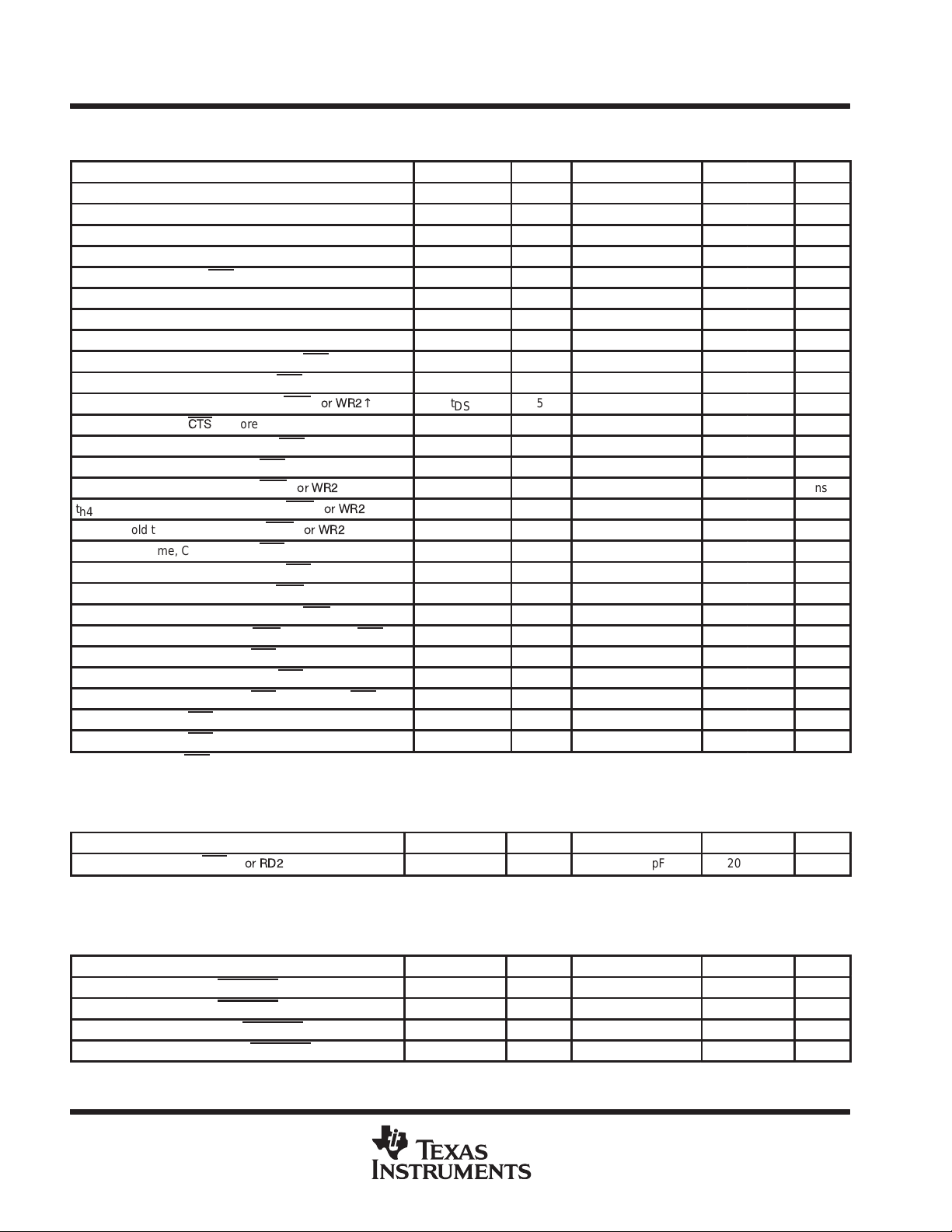
PARAMETER ALT. SYMBOL FIGURE TEST CONDITIONS MIN MAX UNIT
t
Cycle time, read (tw7 + td8 + td9) RC 87 ns
cR
t
Cycle time, write (tw6 + td5 + td6) WC 87 ns
cW
t
Pulse duration, clock (XIN) high t
w1
t
Pulse duration, clock (XIN) low t
w2
t
Pulse duration, ADS low t
w5
t
Pulse duration, write strobe t
w6
t
Pulse duration, read strobe t
w7
t
Pulse duration, MR t
w8
t
Setup time, address valid before ADS↑ t
su1
t
Setup time, CS valid before ADS↑ t
su2
t
Setup time, data valid before WR1↓
su3
†
t
Setup time,
su4
t
Hold time, address low after ADS↑ t
h1
t
Hold time, CS valid after ADS↑ t
h2
t
Hold time, CS valid after WR1↑
h3
†
t
Hold time, address valid after WR1↑
h4
t
Hold time, data valid after WR1↑
h5
t
Hold time, CS valid after RD1↑ or RD2↓
h6
†
t
Hold time, address valid after RD1↑ or RD2↓ t
h7
†
t
Delay time, CS valid before WR1↓ or WR2↑ t
d4
t
Delay time, address valid before WR1↓ or WR2↑ t
d5
†
t
Delay time, write cycle, WR1↑ or WR2↓ to ADS↓ t
d6
†
t
Delay time, CS valid to RD1↓ or RD2↑ t
d7
†
t
Delay time, address valid to RD1↓ or RD2↑ t
d8
t
Delay time, read cycle, RD1↑ or RD2↓ to ADS↓ tRC 6 40 ns
d9
t
Delay time, RD1↓ or RD2↑ to data valid t
d10
t
Delay time, RD1↑ or RD2↓ to floating data t
d11
†
Only applies when ADS is low
CTS
↑ before midpoint of stop bit
or WR2
or WR2
or WR2
or WR2
XH
XL
ADS
WR
RD
MR
AS
CS
↑
↓
↓
↓
t
DS
AH
CH
t
WCS
t
WA
t
DH
t
RCS
RA
CSW
AW
WC
CSR
AR
RVD
HZ
4 f = 16 MHz maximum 25 ns
4 f = 16 MHz maximum 25 ns
5, 6 9 ns
5 40 ns
6 40 ns
1 µs
5, 6 8 ns
5, 6 8 ns
5 15 ns
16 10 ns
5, 6 0 ns
5, 6 0 ns
5 10 ns
5 10 ns
5 5 ns
6 10 ns
6 20 ns
5 7 ns
5 7 ns
5 40 ns
6 7 ns
6 7 ns
6 CL = 75 pF 45 ns
6 CL = 75 pF 20 ns
system switching characteristics over recommended ranges of supply voltage and operating
free-air temperature (see Note 9)
PARAMETER ALT. SYMBOL FIGURE TEST CONDITIONS MIN MAX UNIT
t
dis(R)
NOTE 9: Charge and discharge times are determined by VOL, VOH, and external loading.
Disable time, RD1↓↑
or RD2
↑↓ to DDIS↑↓ t
RDD
6 CL = 75 pF 20 ns
baud generator switching characteristics over recommended ranges of supply voltage and
operating free-air temperature, C
PARAMETER ALT. SYMBOL FIGURE TEST CONDITIONS MIN MAX UNIT
10
t
t
t
t
w3
w4
d1
d2
Pulse duration, BAUDOUT low t
Pulse duration, BAUDOUT high t
Delay time, XIN↑ to BAUDOUT↑ t
Delay time, XIN↑↓ to BAUDOUT↓ t
= 75 pF
L
LW
HW
BLD
BHD
POST OFFICE BOX 655303 • DALLAS, TEXAS 75265
4 f = 16 MHz, CLK ÷ 2 50 ns
4 f = 16 MHz, CLK ÷ 2 50 ns
4 45 ns
4 45 ns
ASYNCHRONOUS COMMUNICATIONS ELEMENT
PARAMETER
DELAY
DELAY
XIN
XO
PARAMETER
DELAY
DELAY
XIN
XO
WITH 64-BYTE FIFOs AND AUTOFLOW CONTROL
SLLS191C – JANUARY 1995 – REVISED DECEMBER 1997
commercial maximum switching characteristics, VCC = 4.75 V, TJ = 115°C
TL16C750
t
PLH
t
PHL
FROM TO
(INPUT) (OUTPUT)
t
r
t
f
Output rise time, XO 10.86 40.42 69.98 82.65
Output fall time, XO 5.47 20.90 36.34 42.95
INTRINSIC
(ns)
–0.92 0.571 7.65 27.66 47.66 56.23
–0.79 0.312 3.89 14.83 25.76 30.45
DELTA
(ns/pF)
DELAY (ns)
CL = 15 pF CL = 50 pF CL = 85 pF CL = 100 pF
commercial maximum switching characteristics, VCC = 3 V, TJ = 115°C
t
PLH
t
PHL
FROM TO
(INPUT) (OUTPUT)
t
r
t
f
Output rise time, XO 14.39 64.87 115.35 136.98
Output fall time, XO 5.06 26.53 48.01 57.21
INTRINSIC
(ns)
–4.69 1.017 10.57 46.16 81.75 97.00
–3.05 0.442 3.58 19.04 34.51 41.13
DELTA
(ns/pF)
DELAY (ns)
CL = 15 pF CL = 50 pF CL = 85 pF CL = 100 pF
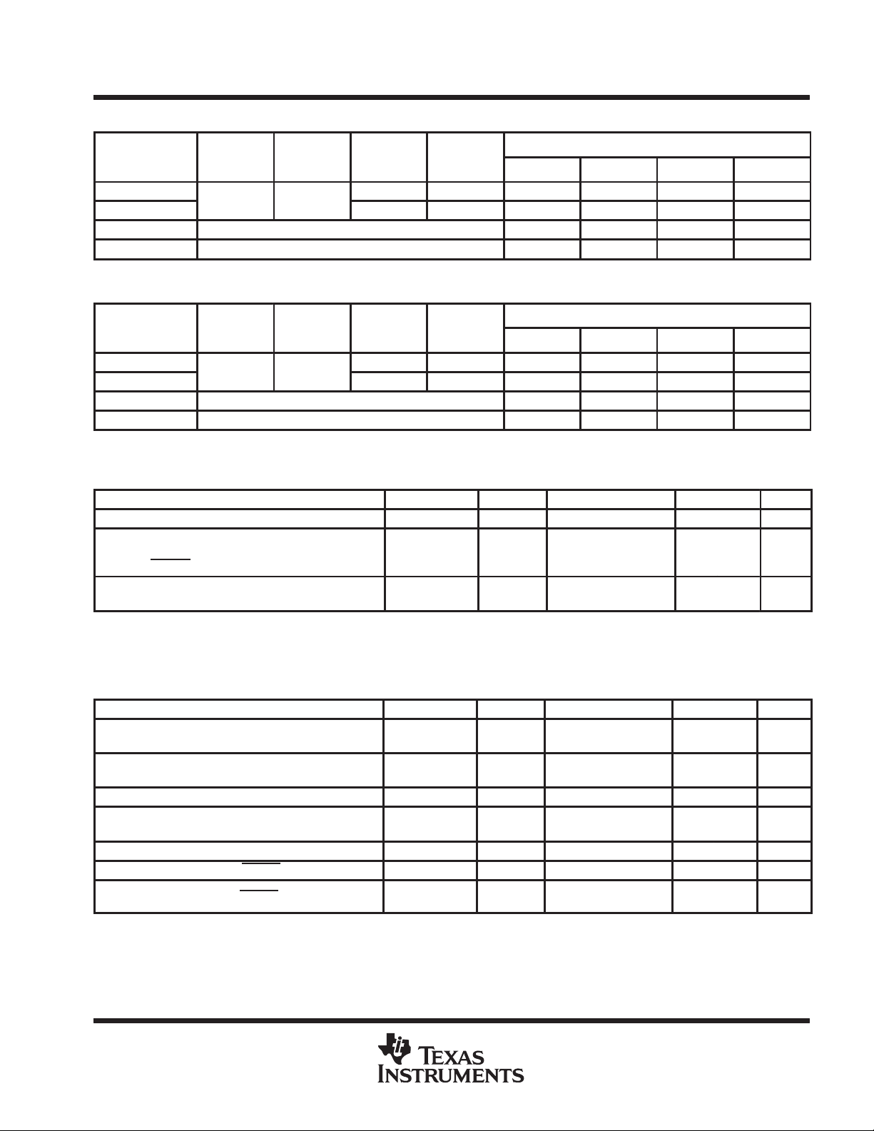
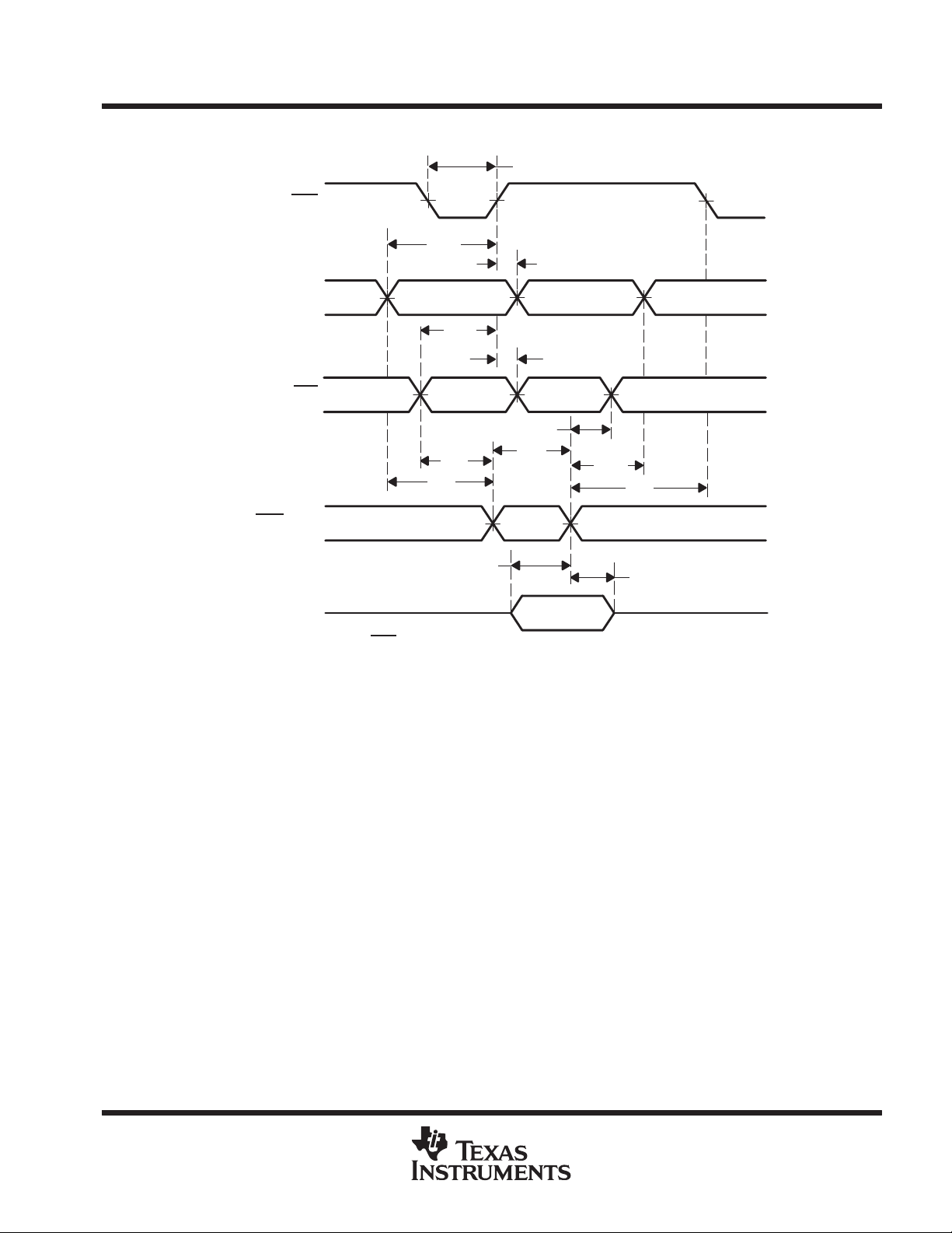
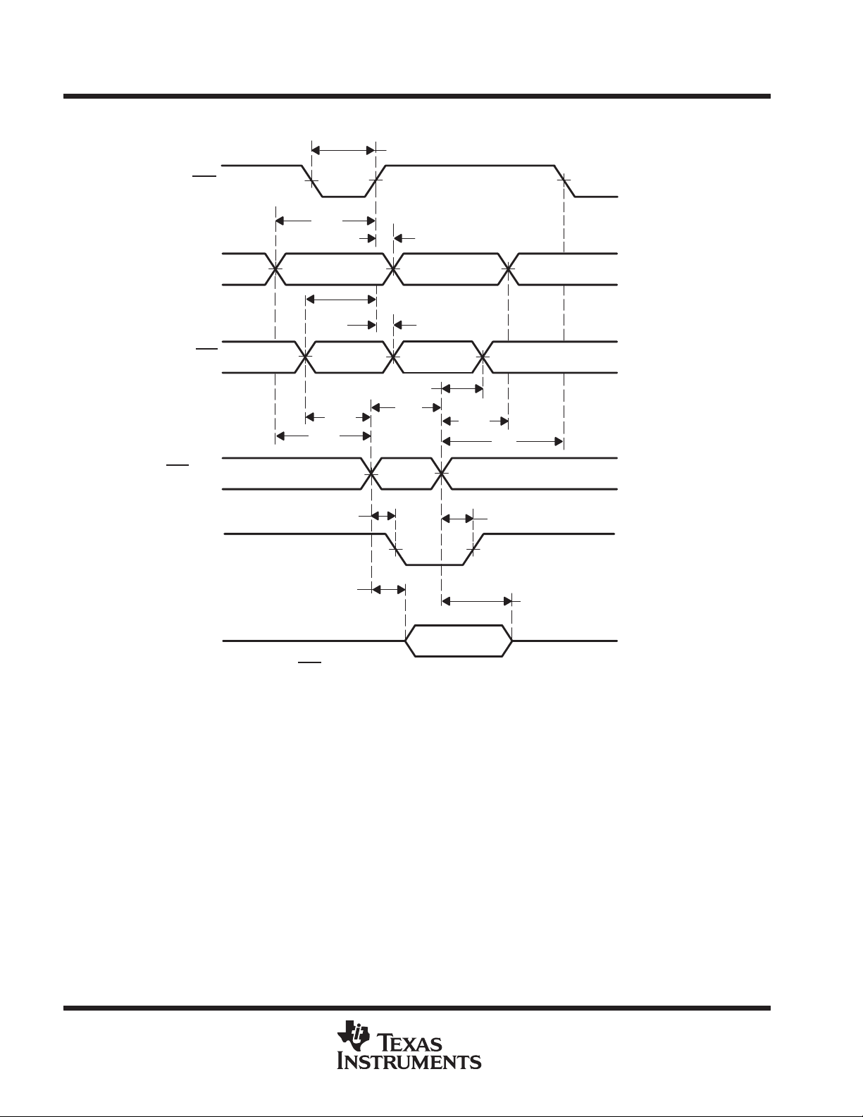
receiver switching characteristics over recommended ranges of supply voltage and operating
free-air temperature (see Note 10)
PARAMETER ALT. SYMBOL FIGURE TEST CONDITIONS MIN MAX UNIT
t
d12
t
d13
t
d14
NOTE 10: In the FIFO mode, the read cycle (RC) = 425 ns (minimum) between reads of the receive FIFO and the status registers (interrupt
Delay time, RCLK to sample clock t
Delay time, stop to set receiver error inter-
rupt or read RBR to LSI interrupt or stop to
RXRDY
↓
Delay time, read RBR/LSR low to reset
interrupt low
identification register or line status register).
SCD
t
SINT
t
RINT
7 10 ns
7, 8, 9,
10, 11
7, 8, 9,
10, 11
CL = 75 pF 120 ns
2
RCLK
cycle
transmitter switching characteristics over recommended ranges of supply voltage and operating
free-air temperature
PARAMETER
t
Delay time, INTRPT to transmit start t
d15
t
Delay time, start to interrupt t
d16
t
Delay time, WR THR to reset interrupt t
d17
t
Delay time, initial write to interrupt (THRE) t
d18
t
Delay time, read IIR to reset interrupt (THRE) t
d19
t
Delay time, write to TXRDY inactive t
d20
t
Delay time, start to TXRDY active
d21
†
THRE = transmitter holding register empty, IIR = interrupt identification register.
†
ALT. SYMBOL FIGURE TEST CONDITIONS MIN MAX UNIT
IRS
STI
HR
WXI
t
SXA
12 8 24
12 8 10
12 CL = 75 pF 50 ns
SI
IR
12 16 34
12 CL = 75 pF 70 ns
13, 14 CL = 75 pF 75 ns
13, 14 CL = 75 pF 9
baudout
cycles
baudout
cycles
baudout
cycles
baudout
cycles
POST OFFICE BOX 655303 • DALLAS, TEXAS 75265
11

TL16C750
ASYNCHRONOUS COMMUNICATIONS ELEMENT
WITH 64-BYTE FIFOs AND AUTOFLOW CONTROL
SLLS191C – JANUARY 1995 – REVISED DECEMBER 1997
modem control switching characteristics over recommended ranges of supply voltage and
= 75 pF
operating free-air temperature, C
PARAMETER ALT. SYMBOL FIGURE MIN MAX UNIT
t
d22
t
d23
t
d24
t
d25
t
d26
t
d27
Delay time, WR MCR to output t
Delay time, modem interrupt to set interrupt t
Delay time, RD MSR to reset interrupt t
Delay time, CTS low to SOUT↓ 16 24
Delay time, receiver threshold byte to RTS↑ 17 2
Delay time, read of last byte in receive FIFO to RTS↓ 17 3
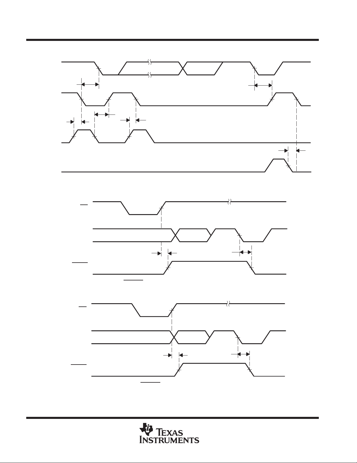
PARAMETER MEASUREMENT INFORMATION
t
w1
L
MDO
SIM
RIM
N
t
w2
15 60 ns
15 35 ns
15 45 ns
baudout
cycles
baudout
cycles
baudout
cycles
XIN
BAUDOUT
(1/1)
BAUDOUT
(1/2)
BAUDOUT
(1/3)
BAUDOUT
(1/N)
(N > 3)
t
d1
t
d1
t
w3
2 XIN Cycles
t
w4
t
d2
t
d2
(N–2) XIN Cycles
12
Figure 4. Baud Generator Timing Waveforms
POST OFFICE BOX 655303 • DALLAS, TEXAS 75265
ASYNCHRONOUS COMMUNICATIONS ELEMENT
WITH 64-BYTE FIFOs AND AUTOFLOW CONTROL
SLLS191C – JANUARY 1995 – REVISED DECEMBER 1997
PARAMETER MEASUREMENT INFORMATION
t
w5
TL16C750
ADS
A0–A2
CS0, CS1, CS2
WR1, WR2
D7–D0
†
Applicable only when ADS
50%50%
t
su1
t
h1
50%
50% 50%
Valid V alid
t
su2
Valid Valid
t
d4
t
d5
50% 50%
t
su3
is low
t
h3
t
w6
Active
Valid Data
t
h2
50%
†
†
t
h4
50%50%
†
t
d6
t
h5
Figure 5. Write Cycle Timing Waveforms
POST OFFICE BOX 655303 • DALLAS, TEXAS 75265
13
TL16C750
ASYNCHRONOUS COMMUNICATIONS ELEMENT
WITH 64-BYTE FIFOs AND AUTOFLOW CONTROL
SLLS191C – JANUARY 1995 – REVISED DECEMBER 1997
PARAMETER MEASUREMENT INFORMATION
t
w5
ADS
A0–A2
CS0, CS1, CS2
RD1, RD2
DDIS
50%
50%
50%50%
t
su1
t
h1
Valid Valid
Valid Valid
†
t
d7
td8†
50% 50%
t
dis(R)
50% 50%
t
su2
t
h2
50%
t
h6
t
w7
Active
50% 50%
50%
†
†
50%
†
t
h7
t
d9
t
dis(R)
D7–D0
†
Applicable only when ADS is low
Figure 6. Read Cycle Timing Waveforms
t
d10
Valid Data
t
d11
14
POST OFFICE BOX 655303 • DALLAS, TEXAS 75265

RCLK
Sample Clock
TL16C450 Mode:
ASYNCHRONOUS COMMUNICATIONS ELEMENT
WITH 64-BYTE FIFOs AND AUTOFLOW CONTROL
SLLS191C – JANUARY 1995 – REVISED DECEMBER 1997
PARAMETER MEASUREMENT INFORMATION
t
8 Clocks
d12
TL16C750
SIN
Sample Clock
INTRPT
(data ready)
INTRPT
(receiver error)
RD1
, RD2
(read RBR)
RD1
, RD2
(read LSR)
Parity StopStart Data Bits 5–8
t
d13
50%
50%
t
Figure 7. Receiver Timing Waveforms
d14
Active
t
d14
50%
50%50%
50%
Active
POST OFFICE BOX 655303 • DALLAS, TEXAS 75265
15

TL16C750
ASYNCHRONOUS COMMUNICATIONS ELEMENT
WITH 64-BYTE FIFOs AND AUTOFLOW CONTROL
SLLS191C – JANUARY 1995 – REVISED DECEMBER 1997
PARAMETER MEASUREMENT INFORMATION
SIN
Sample Clock
Trigger Level
INTRPT
(FCR6, 7 = 0, 0)
Line Status
INTRPT
(LSI)
RD1
(RD LSR)
RD1
(RD RBR)
NOTE A: For a time-out interrupt, t
Figure 8. Receive FIFO First Byte (Sets DR Bit) Waveforms
Data Bits 5–8
= 9 RCLKs.
d13
t
(see Note A)
d13
50%
t
d14
Stop
Active
(FIFO at or above
50%
t
d14
50%50%
50%
50%
Active
trigger level)
(FIFO below
trigger level)
SIN
Sample Clock
Time-Out or
Trigger Level
INTRPT
(see Note A
Line Status
INTRPT (LSI)
RD1, RD2
(RD LSR)
, RD2
RD1
(RD RBR)
Previous Byte
Read From FIFO
NOTE A: For a time-out interrupt, t
Stop
50%
t
d13
)
Top Byte of FIFO
t
d13
Active Active
= 9 RCLKs.
d13
50% 50%
t
d14
t
d14
50%
50%50%
50%
(FIFO at or above
trigger level)
(FIFO below
trigger level)
Figure 9. Receive FIFO Bytes Other Than the First Byte (DR Internal Bit Already Set) Waveforms
16
POST OFFICE BOX 655303 • DALLAS, TEXAS 75265

ASYNCHRONOUS COMMUNICATIONS ELEMENT
WITH 64-BYTE FIFOs AND AUTOFLOW CONTROL
SLLS191C – JANUARY 1995 – REVISED DECEMBER 1997
PARAMETER MEASUREMENT INFORMATION
TL16C750
RD
(RD RBR)
SIN
(first byte)
Sample Clock
(see Note B)
RXRDY
NOTES: A. This is the reading of the last byte in the FIFO.
B. For a time-out interrupt, t
t
d13
Stop
50%
= 9 RCLKs.
d13
t
50%
d14
Active
See Note A
50%
Figure 10. Receiver Ready (RXRDY) Waveforms, FCR0 = 0 or FCR0 = 1 and FCR3 = 0 (Mode 0)
RD
(RD RBR)
SIN
(first byte that reaches
the trigger level)
50%
Active
See Note A
Sample Clock
t
(see Note B)
RXRDY
NOTES: A. This is the reading of the last byte in the FIFO.
B. For a time-out interrupt, t
d13
= 9 RCLKs.
d13
t
d14
50%50%
Figure 11. Receiver Ready (RXRDY) Waveforms, FCR0 = 1 and FCR3 = 1 (Mode 1)
POST OFFICE BOX 655303 • DALLAS, TEXAS 75265
17
TL16C750
ASYNCHRONOUS COMMUNICATIONS ELEMENT
WITH 64-BYTE FIFOs AND AUTOFLOW CONTROL
SLLS191C – JANUARY 1995 – REVISED DECEMBER 1997
PARAMETER MEASUREMENT INFORMATION
SOUT
INTRPT
(THRE)
WR THR
RD IIR
Start
50%
t
d15
50% 50% 50% 50% 50%
t
d18
t
d17
50%
50%
Data Bits
50%
t
d17
Parity Stop
t
d16
Start
50%
Figure 12. Transmitter Timing Waveforms
WR
(WR THR)
SOUT
Byte #1
Data
50%
Parity
Stop
Start
50%
t
d19
50%
t
d21
50%
TXRDY
t
d20
50%
Figure 13. Transmitter Ready (TXRDY) Waveforms, FCR0 = 0 or FCR0 = 1 and FCR3 = 0 (Mode 0)
WR
(WR THR)
SOUT
TXRDY
Data
Byte #16
t
d20
50%
50%
Parity
Stop
t
FIFO Full
Start
50%
d21
50%
Figure 14. Transmitter Ready (TXRDY) Waveforms, FCR0 = 1 and FCR3 = 1 (Mode 1)
18
POST OFFICE BOX 655303 • DALLAS, TEXAS 75265

ASYNCHRONOUS COMMUNICATIONS ELEMENT
WITH 64-BYTE FIFOs AND AUTOFLOW CONTROL
SLLS191C – JANUARY 1995 – REVISED DECEMBER 1997
PARAMETER MEASUREMENT INFORMATION
TL16C750
WR
(WR MCR)
RTS, DTR,
OUT1
, OUT2
CTS, DSR, DCD
INTRPT
(modem)
RD2
(RD MSR)
RI
50% 50%
t
d22
50% 50%
50%
t
d23
t
50%
d24
50%
50%
Figure 15. Modem Control Timing Waveforms
t
d22
50%
50%
t
d23
CTS
SOUT
SIN
RTS
RBRRD
50% 50%
t
d25
50%
Midpoint of Stop Bit
Figure 16. CTS and SOUT Autoflow Control Timing (Start and Stop) Waveforms
Midpoint of Stop Bit
t
d26
50%
t
50%
d27
50%
Figure 17. Auto-RTS Timing for Receiver Threshold at All Trigger Levels Waveforms
t
su4
POST OFFICE BOX 655303 • DALLAS, TEXAS 75265
19

TL16C750
ASYNCHRONOUS COMMUNICATIONS ELEMENT
WITH 64-BYTE FIFOs AND AUTOFLOW CONTROL
SLLS191C – JANUARY 1995 – REVISED DECEMBER 1997
PARAMETER MEASUREMENT INFORMATION
C
P
U
B
U
S
D7–D0
MEMR
or I/OR
MEMW or I/ON
INTR
RESET
A0
A1
A2
L
CS
H
D7–D0
RD
1
1
WR
INTRPT
MR
A0
A1
A2
ADS
WR2
RD2
CS2
CS1
CS0
TL16C750
(ACE)
SOUT
SIN
RTS
DTR
DSR
DCD
CTS
RI
XIN
XOUT
BAUDOUT
RCLK
232-D Drivers
and Receivers
Figure 18. Basic TL16C750 Configuration
EIA
3.072 MHz
Microcomputer
System
Figure 19. Typical Interface for a High-Capacity Data Bus
APPLICATION INFORMATION
WR
Data Bus Data Bus
8-Bit
Bus Transceiver
Receiver Disable
Driver Disable
WR1
TL16C750
(ACE)
D7–D0
DDIS
20
POST OFFICE BOX 655303 • DALLAS, TEXAS 75265

ASYNCHRONOUS COMMUNICATIONS ELEMENT
WITH 64-BYTE FIFOs AND AUTOFLOW CONTROL
SLLS191C – JANUARY 1995 – REVISED DECEMBER 1997
APPLICATION INFORMATION
TL16C750
A16–A23
CPU
RSI/ABT
AD0–AD15
PHI1 PHI2
ADS
Address
Decoder
Buffer
A16–A23
AD0–AD7
14
15
16
28
39
TL16C750
CS0
CS1
CS2
ADS
MR
A0–A2
D0–D2
XIN
XOUT
BAUDOUT
RCLK
DTR
RTS
OUT1
OUT2
DCD
DSR
CTS
Alternate
18
19
17
10
37
36
38
35
43
RI
42
41
40
Crystal Control
20
1
8
6
5
RSTO
PHI1 PHI2
NOTE A: Terminal numbers shown are for the FN package.
ADS
RD
TCU
WR
AD0–AD15
Figure 20. Typical TL16C750 Connection to a CPU
24
20
25
GND
(VSS)
RD1
WR1
RD2
WR2
SOUT
SIN
INTRPT
TXRDY
DDIS
RXRDY
22 44
5 V
(VCC)
13
11
33
27
26
3221
2
3
7
1
EIA-232-D
Connector
POST OFFICE BOX 655303 • DALLAS, TEXAS 75265
21

TL16C750
ASYNCHRONOUS COMMUNICATIONS ELEMENT
WITH 64-BYTE FIFOs AND AUTOFLOW CONTROL
SLLS191C – JANUARY 1995 – REVISED DECEMBER 1997
PRINCIPLES OF OPERATION
Table 1. Register Selection
†
DLAB
0 L L L Receiver buffer (read), transmitter holding register (write)
0 L L H Interrupt enable register
X L H L Interrupt identification register (read only)
X L H L FIFO control register (write)
X L H H Line control register
X H L L Modem control register
X H L H Line status register
X H H L Modem status register
X H H H Scratch register
1 L L L Divisor latch (LSB)
1 L L H Divisor latch (MSB)
†
The divisor latch access bit (DLAB) is the most significant bit of the line control register . The DLAB signal
is controlled by writing to this bit location (see Table 3).
A2 A1 A0 REGISTER
Table 2. ACE Reset Functions
REGISTER/SIGNAL
Interrupt Enable Register Master Reset All bits cleared (0–5 forced and 6–7 permanent)
Interrupt Identification Register Master Reset Bit 0 is set, bits 1–4 are cleared, and bits 5–7 are cleared
FIFO Control Register Master Reset All bits cleared
Line Control Register Master Reset All bits cleared
Modem Control Register Master Reset All bits cleared (6–7 permanent)
Line Status Register Master Reset Bits 5 and 6 are set, all other bits are cleared
Modem Status Register Master Reset Bits 0–3 are cleared, bits 4–7 are input signals
SOUT Master Reset High
INTRPT (receiver error flag) Read LSR/MR Low
INTRPT (received data available) Read RBR/MR Low
INTRPT (transmitter holding register empty) Read IR/Write THR/MR Low
INTRPT (modem status changes) Read MSR/MR Low
OUT2 Master Reset High
RTS Master Reset High
DTR Master Reset High
OUT1 Master Reset High
Scratch Register Master Reset No effect
Divisor Latch (LSB and MSB) Registers Master Reset No effect
Receiver Buffer Registers Master Reset No effect
Transmitter Holding Registers Master Reset No effect
Receiver FIFO
XMIT FIFO
RESET
CONTROL
MR/FCR1–FCR0/
∆FCR0
MR/FCR2–FCR0/
∆FCR0
RESET STATE
All bits cleared
All bits cleared
22
POST OFFICE BOX 655303 • DALLAS, TEXAS 75265

ASYNCHRONOUS COMMUNICATIONS ELEMENT
WITH 64-BYTE FIFOs AND AUTOFLOW CONTROL
SLLS191C – JANUARY 1995 – REVISED DECEMBER 1997
PRINCIPLES OF OPERATION
accessible registers
The system programmer, through the CPU, has access to and control over any of the ACE registers. These
registers control ACE operations, receive data, and transmit data. Descriptions of these registers follow in
Table 3.
Table 3. Summary of Accessible Registers
REGISTER ADDRESS
0DLAB=0 0 DLAB = 0 1DLAB=0 2 2 3 4 5 6 7 0 DLAB = 1 1 DLAB = 1
Receiver
Bit
Buffer
No.
Register
(Read
Only)
RBR THR IER IIR FCR LCR MCR LSR MSR SCR DLL DLM
0 Data Bit 0†Data Bit 0
1 Data Bit 1 Data Bit 1
2 Data Bit 2 Data Bit 2
3 Data Bit 3 Data Bit 3
4 Data Bit 4 Data Bit 4
5 Data Bit 5 Data Bit 5
6 Data Bit 6 Data Bit 6 0
7 Data Bit 7 Data Bit 7 0
†
Bit 0 is the least significant bit. It is the first bit serially transmitted or received.
‡
Access to DLAB LSB, MSB, and FCR bit 5 require LCR bit 7 = 1
NOTE 11: These bits are always 0 in the TL16C450 mode.
Transmitter
Holding
Register
(Write
Only)
Interrupt
Enable
Register
Enable
Received
Data
Available
Interrupt
(ERBI)
Enable
Transmitter
Holding
Register
Empty
Interrupt
(ETBEI)
Enable
Receiver
Line Status
Interrupt
(ELSI)
Enable
Modem
Status
Interrupt
(EDSSI)
Sleep Mode
Enable
Low Power
Mode Enable
Interrupt
Ident.
Register
(Read
Only)
0 when
interrupt
Pending
Interrupt
ID
Bit 1
Interrupt
ID
Bit 2
Interrupt
ID
Bit 2
(see
Note 4)
0 Reserved
64 Byte
FIFO
Enabled
FIFOs
Enabled
(see
Note 11)
FIFOs
Enabled
(see
Note 11)
FIFO
Control
Register
(Write
Only)
FIFO
Enable
Receiver
FIFO
Reset
Transmitter
FIFO
Reset
DMA
Mode
Select
64 Byte
FIFO
Enable
Receiver
Trigger
(LSB)
Receiver
Trigger
(MSB)
Line
Control
Register
Word
Length
Select
Bit 0
(WLS0)
Word
Length
Select
Bit 1
(WLS1)
Number
Stop Bits
(STB)
Parity
Enable
(PEN)
Even
Parity
Select
(EPS)
Stick
Parity
‡
Break
Control
Divisor
Latch
Access
(DLAB)
Modem
Control
Register
Data
Terminal
Ready
(DTR)
Request
to Send
(RTS)
of
Bit
OUT1
OUT2
Loop
Flow
Control
Enable
(AFE)
0
0
‡
Line
Status
Register
Data
Ready
(DR)
Overrun
Error
(OE)
Parity
Error
(PE)
Framing
Error
(FE)
Break
Interrupt
(BI)
Transmitter
Holding
Register
(THRE)
Transmitter
Empty
(TEMT)
Error in
Receiver
FIFO
(see
Note 12)
Modem
Status
Register
Delta
Clear
to Send
∆CTS)
(
Delta
Data
Set
Ready
∆DSR)
(
Trailing
Edge Ring
Indicator
(TERI)
Delta
Data
Carrier
Detect
∆DCD)
(
Clear
to
Send
(CTS)
Data
Set
Ready
(DSR)
Ring
Indicator
(RI)
Data
Carrier
Detect
(DCD)
Scratch
Register
Bit 0 Bit 0 Bit 8
Bit 1 Bit 1 Bit 9
Bit 2 Bit 2 Bit 10
Bit 3 Bit 3 Bit 11
Bit 4 Bit 4 Bit 12
Bit 5 Bit 5 Bit 13
Bit 6 Bit 6 Bit 14
Bit 7 Bit 7 Bit 15
Divisor
Latch
(LSB)
TL16C750
Latch
(MSB)
POST OFFICE BOX 655303 • DALLAS, TEXAS 75265
23

TL16C750
ASYNCHRONOUS COMMUNICATIONS ELEMENT
WITH 64-BYTE FIFOs AND AUTOFLOW CONTROL
SLLS191C – JANUARY 1995 – REVISED DECEMBER 1997
PRINCIPLES OF OPERATION
FIFO control register (FCR)
The FCR is a write-only register at the same location as the IIR, which is a read-only register. The FCR enables
the FIFOs, clears the FIFOs, sets the receiver FIFO trigger level, and selects the type of DMA signaling.
D
Bit 0: FCR0 when set enables the transmit and receive FIFOs. This bit must be set when other FCR bits
are written to or they are not programmed. Changing this bit clears the FIFOs.
D
Bit 1: FCR1 when set clears all bytes in the receiver FIFO and resets its counter . The RSR is not cleared.
The logic 1 that is written to this bit position is self clearing.
D
Bit 2: FCR2 when set clears all bytes in the transmit FIFO and resets its counter to 0. The TSR is not
cleared. The logic 1 that is written to this bit position is self clearing.
D
Bit 3: When FCR0 is set, setting FCR3 causes the RXRDY and TXRDY to change from mode 0 to
mode 1.
D
Bit 4: Reserved for future use.
D
Bit 5: When this bit is set 64-byte mode of operation is selected. When cleared, the 16-byte mode is
selected. A write to FCR bit 5 is protected by setting the line control register (LCR) bit 7 = 1. LCR bit 7 needs
to cleared for normal operation.
D
Bits 6 and 7: FCR6 and FCR7 set the trigger level for the receiver FIFO interrupt (see Table 4).
Table 4. Receiver FIFO Trigger Level
BIT 7 BIT 6
0 0 01 01
0 1 04 16
1 0 08 32
1 1 14 56
16-BYTE RECEIVER FIFO
TRIGGER LEVEL (BYTES)
64-BYTE RECEIVER FIFO
TRIGGER LEVEL (BYTES)
FIFO interrupt mode operation
When the receiver FIFO and receiver interrupts are enabled (FCR0 = 1, IER0 = 1, IER2 = 1), a receiver interrupt
occurs as follows:
1. The received data available interrupt is issued to the microprocessor when the FIFO has reached its
programmed trigger level. It is cleared when the FIFO drops below its programmed trigger level.
2. The IIR receive data available indication also occurs when the FIFO trigger level is reached, and as the
interrupt, is cleared when the FIFO drops below the trigger level.
3. The receiver line status interrupt (IIR = 06 or 0110h) has higher priority than the received data available (IIR
= 04) interrupt.
4. The data ready bit (LSR0) is set when a character is transferred from the shift register to the receiver FIFO.
It is cleared when the FIFO is empty.
When the receiver FIFO and receiver interrupts are enabled:
24
POST OFFICE BOX 655303 • DALLAS, TEXAS 75265

ASYNCHRONOUS COMMUNICATIONS ELEMENT
WITH 64-BYTE FIFOs AND AUTOFLOW CONTROL
SLLS191C – JANUARY 1995 – REVISED DECEMBER 1997
PRINCIPLES OF OPERATION
FIFO interrupt mode operation (continued)
1. FIFO time-out interrupt occurs when the following conditions exist:
a. At least one character is in the FIFO.
b. The most recent serial character was received more than four continuous character times ago (if two
stop bits are programmed, the second one is included in this time delay).
c. The most recent microprocessor read of the FIFO occurred more than four continuous character times
ago. This causes a maximum character received to interrupt an issued delay of 160 ms at
300 baud with a 12-bit character.
2. Character times are calculated by using RCLK for a clock signal (makes the delay proportional to the baud
rate).
3. When a time-out interrupt has occurred, the FIFO interrupt is cleared. The timer is reset when the
microprocessor reads one character from the receiver FIFO. When a time-out interrupt has not occurred,
the time-out timer is reset after a new character is received or after the microprocessor reads the receiver
FIFO.
TL16C750
When the transmitter FIFO and THRE interrupt are enabled (FCR0 = 1, IER1 = 1), transmit interrupts occur as
follows:
1. The transmitter holding register interrupt [IIR (3 –0) = 2] occurs when the transmit FIFO is empty. The
transmit FIFO is cleared [IIR (3–0) = 1] when the THR is written to (1 to 16 characters may be written to
the transmit FIFO while servicing this interrupt) or the IIR is read.
2. The transmit FIFO empty indicator (LSR5 (THRE) = 1) is delayed one character time minus the last stop
bit time when there have not been at least two bytes in the transmit FIFO at the same time since the last
time that THRE = 1. The first transmitter interrupt after changing FCR0 is immediate when it is enabled.
Character time-out and receiver FIFO trigger level interrupts have the same priority as the current received data
available interrupt; transmit FIFO empty has the same priority as the current THRE interrupt.
FIFO polled mode operation
With FCR0 = 1 (transmitter and receiver FIFOs enabled), clearing IER0, IER1, IER2, IER3, or all four to 0 puts
the ACE in the FIFO polled mode of operation. Since the receiver and transmitter are controlled separately,
either one or both can be in the polled mode of operation.
In this mode, the user program checks receiver and transmitter status using the LSR. As stated previously:
• LSR0 is set when there is at least one byte in the receiver FIFO.
• LSR (1–4) specify which error(s) have occurred. Character error status is handled the same way as
when in the interrupt mode; the IIR is not affected since IER2 = 0.
• LSR5 indicates when the THR is empty.
• LSR6 indicates that both the THR and TSR are empty.
• LSR7 indicates whether there are any errors in the receiver FIFO.
There is no trigger level reached or time-out condition indicated in the FIFO polled mode. However, the receiver
and transmitter FIFOs are still fully capable of holding characters.
POST OFFICE BOX 655303 • DALLAS, TEXAS 75265
25

TL16C750
ASYNCHRONOUS COMMUNICATIONS ELEMENT
WITH 64-BYTE FIFOs AND AUTOFLOW CONTROL
SLLS191C – JANUARY 1995 – REVISED DECEMBER 1997
PRINCIPLES OF OPERATION
interrupt enable register (IER)
The IER enables each of the five types of interrupts (refer to Table 5) and the INTRPT signal in response to an
interrupt generation. The IER can also disable the interrupt system by clearing bits 0 through 3. The contents
of this register are summarized in Table3 and are described in the following bulleted list.
D
Bit 0: When set, this bit enables the received data available interrupt.
D
Bit 1: When set, this bit enables the THRE interrupt.
D
Bit 2: When set, this bit enables the receiver line status interrupt.
D
Bit 3: When set, this bit enables the modem status interrupt.
D
Bit 4: When set, this bit enables sleep mode. The ACE is always awake when there is a byte in the
transmitter, activity on the SIN, or when the device is in the loopback mode. The ACE is also awake when
either ∆CTS, ∆DSR, ∆DCD, or TERI = 1. Bit 4 must be set to enable sleep mode.
D
Bit 5: When set, this bit enables low-power mode. Low-power mode functions similar to sleep mode.
However, this feature powers down the clock to the ACE only , while keeping the oscillator running. Bit 5 must
be set to enable low-power mode.
D
Bits 6 and 7: Not used (always cleared)
interrupt identification register (IIR)
The ACE has an on-chip interrupt generation and prioritization capability that permits a flexible interface with
most popular microprocessors.
The ACE provides four prioritized levels of interrupts:
D
Priority 1–Receiver line status (highest priority)
D
Priority 2–Receiver data ready or receiver character timeout
D
Priority 3–Transmitter holding register empty
D
Priority 4–Modem status (lowest priority)
When an interrupt is generated, the IIR indicates that an interrupt is pending and provides the type of interrupt
in its three least significant bits (bits 0, 1, and 2). The contents of this register are summarized in Table 3 and
described in Table 5. Details on each bit are as follows:
D
Bit 0: This bit can be used either in a hardwire prioritized, or polled interrupt system. When this bit is cleared,
an interrupt is pending. When bit 0 is set, no interrupt is pending.
D
Bits 1 and 2: Used to identify the highest priority interrupt pending as indicated in Table 3.
D
Bit 3: This bit is always cleared in the TL16C450 mode. In FIFO mode, this bit is set with bit 2 to indicate
that a time-out interrupt is pending.
D
Bit 4: Not used (always cleared)
26
D
Bits 5, 6, and 7: These bits are to verify the FIFO operation. When all 3 bits are cleared, TL16C450 mode
is chosen. When bits 6 and 7 are set and bit 5 is cleared, 16-byte mode is chosen. When bits 5, 6, and 7
are set, 64-byte mode is chosen.
POST OFFICE BOX 655303 • DALLAS, TEXAS 75265
ASYNCHRONOUS COMMUNICATIONS ELEMENT
WITH 64-BYTE FIFOs AND AUTOFLOW CONTROL
SLLS191C – JANUARY 1995 – REVISED DECEMBER 1997
PRINCIPLES OF OPERATION
interrupt identification register (IIR) (continued)
Table 5. Interrupt Control Functions
INTERRUPT
IDENTIFICATION
REGISTER
BIT 3 BIT 2 BIT 1 BIT 0
0 0 0 1 None None None None
0 1 1 0 1 Receiver line status
0 1 0 0 2 Received data available
1 1 0 0 2
0 0 1 0 3
0 0 0 0 4 Modem status
PRIORITY
LEVEL
INTERRUPT TYPE INTERRUPT SOURCE
Overrun error, parity error,
framing error or break interrupt
Receiver data available in the
TL16C450 mode or trigger level
reached in the FIFO mode.
No characters have been
Character time-out
indication
Transmitter holding
register empty
removed from or input to the
receiver FIFO during the last
four character times, and there
is at least one character in it
during this time
Transmitter holding register
empty
Clear to send, data set ready,
ring indicator, or data carrier
detect
INTERRUPT RESET
Reading the line status register
Reading the receiver buffer
register
Reading the receiver buffer
register
Reading the interrupt
identification register (if source
of interrupt) or writing into the
transmitter holding register
Reading the modem status
register
TL16C750
METHOD
line control register (LCR)
The system programmer controls the format of the asynchronous data communication exchange through the
LCR. In addition, the programmer is able to retrieve, inspect, and modify the contents of the LCR; this eliminates
the need for separate storage of the line characteristics in system memory. The contents of this register are
summarized in Table 3 and described in the following bulleted list.
D
Bits 0 and 1: These two bits specify the number of bits in each transmitted or received serial character.
These bits are encoded as shown in Table 6.
Table 6. Serial Character Word Length
BIT 1 BIT 0 WORD LENGTH
0 0 5 bits
0 1 6 bits
1 0 7 bits
1 1 8 bits
D
Bit 2: This bit specifies either one, one and one-half, or two stop bits in each transmitted character . When
bit 2 is cleared, one stop bit is generated in the data. When bit 2 is set, the number of stop bits generated
is dependent on the word length selected with bits 0 and 1. The receiver clocks only the first stop bit,
regardless of the number of stop bits selected. The number of stop bits generated, in relation to word length
and bit 2, is shown in Table 7.
POST OFFICE BOX 655303 • DALLAS, TEXAS 75265
27

TL16C750
ASYNCHRONOUS COMMUNICATIONS ELEMENT
WITH 64-BYTE FIFOs AND AUTOFLOW CONTROL
SLLS191C – JANUARY 1995 – REVISED DECEMBER 1997
PRINCIPLES OF OPERATION
line control register (LCR) (continued)
Table 7. Number of Stop Bits Generated
BIT 2
D
Bit 3: This bit is the parity enable bit. When bit 3 is set, a parity bit is generated in data transmitted between
WORD LENGTH SELECTED
BY BITS 1 AND 2
0 Any word length 1
1 5 bits 1 1/2
1 6 bits 2
1 7 bits 2
1 8 bits 2
NUMBER OF STOP
BITS GENERATED
the last data word bit and the first stop bit. In received data, when bit 3 is set, parity is checked. When bit
3 is cleared, no parity is generated or checked.
D
Bit 4: This bit is the even parity select bit. When parity is enabled (bit 3 is set) and bit 4 is set, even parity
(an even number of logic 1s in the data and parity bits) is selected. When parity is enabled and bit 4 is
cleared, odd parity (an odd number of logic 1s) is selected.
D
Bit 5: This is the stick parity bit. When bits 3, 4, and 5 are set, the parity bit is transmitted and checked as
cleared. When bits 3 and 5 are set and bit 4 is cleared, the parity bit is transmitted and checked as set. When
bit 5 is cleared, stick parity is disabled.
D
Bit 6: This bit is the break control bit. Bit 6 is set to force a break condition; i.e., a condition where SOUT
is forced to the spacing (low) state. When bit 6 is cleared, the break condition is disabled and has no affect
on the transmitter logic; it only affects the serial output.
D
Bit 7: This bit is the divisor latch access bit (DLAB). Bit 7 must be set to access the divisor latches of the
baud generator during a read or write or access bit 5 of the FCR. Bit 7 must be cleared during a read or write
to access the receiver buffer, the THR, or the IER.
line status register (LSR)
†
The LSR provides information to the CPU concerning the status of data transfers. The contents of this register
are described in the following bulleted list and summarized in Table 3.
D
Bit 0: This bit is the data ready (DR) indicator for the receiver . DR is set when a complete incoming character
is received and transferred into the RBR or the FIFO. DR is cleared by reading all of the data in the RBR
or the FIFO.
D
Bit 1‡: This bit is the overrun error (OE) indicator . When OE is set, it indicates that before the character in
the RBR was read, it was overwritten by the next character transferred into the register. OE is cleared every
time the CPU reads the contents of the LSR. When the FIFO mode data continues to fill the FIFO beyond
the trigger level, an OE occurs only after the FIFO is full and the next character has been completely
received in the shift register. An OE is indicated to the CPU as soon as it happens. The character in the shift
register is overwritten, but it is not transferred to the FIFO.
D
Bit 2‡: This bit is the parity error (PE) indicator. When PE is set, it indicates that the parity of the received
data character does not match the parity selected in the LCR (bit 4). PE is cleared every time the CPU reads
the contents of the LSR. In the FIFO mode, PE is associated with the particular character in the FIFO to
which it applies. PE is revealed to the CPU when its associated character is at the top of the FIFO.
†
The line status register is intended for read operations only; writing to this register is not recommended outside of a factory testing environment.
‡
Bits 1 through 4 are the error conditions that produce a receiver line status interrupt.
28
POST OFFICE BOX 655303 • DALLAS, TEXAS 75265

ASYNCHRONOUS COMMUNICATIONS ELEMENT
WITH 64-BYTE FIFOs AND AUTOFLOW CONTROL
SLLS191C – JANUARY 1995 – REVISED DECEMBER 1997
PRINCIPLES OF OPERATION
TL16C750
line status register (LSR)
D
Bit 3‡: This bit is the framing error (FE) indicator. When FE is set, it indicates that the received character
does not have a valid (set) stop bit. FE is cleared every time the CPU reads the contents of the LSR. In the
FIFO mode, this error is associated with the particular character in the FIFO to which it applies. FE is
revealed to the CPU when its associated character is at the top of the FIFO. The ACE tries to resynchronize
after a FE. To accomplish this, it is assumed that the FE is due to the next start bit. The ACE samples this
start bit twice and then accepts the input data.
D
Bit 4: This bit is the break interrupt (BI) indicator. When BI is set, it indicates that the received data input
was held in the low state for longer than a full-word transmission time. A full-word transmission time is
defined as the total time to transmit the start, data, parity, and stop bits. BI is cleared every time the CPU
reads the contents of the LSR. In the FIFO mode, BI is associated with the particular character in the FIFO
to which it applies. BI is revealed to the CPU when its associated character is at the top of the FIFO. When
a break occurs, only one 0 character is loaded into the FIFO. The next character transfer is enabled after
SIN goes to the marking state for at least two RCLK samples and then receives the next valid start bit.
D
Bit 5: This bit is the transmitter holding register empty (THRE) indicator. THRE is set when the THR is
empty, indicating that the ACE is ready to accept a new character. If the THRE interrupt is enabled when
THRE is set, an interrupt is generated. THRE is set when the contents of the THR are transferred to the
TSR. THRE is cleared concurrent with the loading of the THR by the CPU. In the FIFO mode, THRE is set
when the transmit FIFO is empty; it is cleared when at least one byte is written to the transmit FIFO.
D
Bit 6: This bit is the transmitter empty (TEMT) indicator. TEMT bit is set when the THR and the TSR are
both empty . When either the THR or the TSR contains a data character, TEMT is cleared. In the FIFO mode,
TEMT is set when the transmitter FIFO and TSR are both empty.
†
(continued)
D
Bit 7: In TL16C750 mode and in TL16C450 mode, this bit is always cleared. In the FIFO mode, LSR7 is
set when there is at least one parity, framing, or break error in the FIFO. It is cleared when the
microprocessor reads the LSR and there are no subsequent errors in the FIFO.
modem control register (MCR)
The MCR is an 8-bit register that controls an interface with a modem, data set, or peripheral device that is
emulating a modem. The contents of this register are summarized in T able 3 and are described in the following
bulleted list.
D
Bit 0: This bit (DTR) controls the DTR output.
D
Bit 1: This bit (RTS) controls RTS output.
D
Bit 2: This bit (OUT1) controls OUT1 signal.
D
Bit 3: This bit (OUT2) controls the OUT2 signal.
When any of bits 0 through 3 is set, the associated output is forced low; a cleared bit forces the associated output
high.
†
The line status register is intended for read operations only; writing to this register is not recommended outside of a factory testing environment.
‡
Bits 1 through 4 are the error conditions that produce a receiver line status interrupt.
POST OFFICE BOX 655303 • DALLAS, TEXAS 75265
29
TL16C750
ASYNCHRONOUS COMMUNICATIONS ELEMENT
WITH 64-BYTE FIFOs AND AUTOFLOW CONTROL
SLLS191C – JANUARY 1995 – REVISED DECEMBER 1997
PRINCIPLES OF OPERATION
modem control register (MCR) (continued)
D
Bit 4: This bit (LOOP) provides a local loop back feature for diagnostic testing of the ACE. When LOOP
is set, the following occurs:
– SOUT is asserted high.
– SIN is disconnected.
– The output of the TSR is looped back into the RSR input.
– The four modem control inputs (CTS
– The four modem control outputs (DTR
, DSR, DCD, and RI) are disconnected.
, RTS, OUT1, and OUT2) are internally connected to the four
modem control inputs.
– The four modem control outputs are forced to their inactive (high) states.
D
Bit 5: This bit (AFE) is the autoflow control enable. When bit 5 is set, the autoflow control, as described in
the detailed description, is enabled.
In the diagnostic mode, data that is transmitted is immediately received. This allows the processor to verify
the transmit and receive data paths to the ACE. The receiver and transmitter interrupts are fully operational.
The modem control interrupts are also operational, but the modem control interrupt sources are now the
lower four bits of the MCR instead of the four modem control inputs. All interrupts are still controlled by the
IER.
The ACE flow can be configured by programming bits 1 and 5 of the MCR as shown in Table 8.
Table 8. ACE Flow Configuration
MCR BIT 5
(AFE)
1 1 Auto-RTS and auto-CTS enabled (autoflow control enabled)
1 0 Auto-CTS only enabled
0 X Auto-RTS and auto-CTS disabled
MCR BIT 1
(RTS)
ACE FLOW CONFIGURATION
When bit 5 of the FCR is cleared, there is a 16-byte AFC. When bit 5 of the FCR is set, there is a 64-byte AFC.
modem status register (MSR)
The MSR is an 8-bit register that provides information about the current state of the control lines from the
modem, data set, or peripheral device to the CPU. Additionally, four bits of this register provide change
information. When a control input from the modem changes state, the appropriate bit is set. All four bits are
cleared when the CPU reads the MSR. The contents of this register are summarized in Table 3 and are
described in the following bulleted list.
D
Bit 0: This bit is the change in clear-to-send (∆CTS) indicator. ∆CTS indicates that CTS has changed states
since the last time it was read by the CPU. When ∆ CTS is set (autoflow control is not enabled and the
modem status interrupt is enabled), a modem status interrupt is generated. When autoflow control is
enabled, no interrupt is generated. When ∆CTS is set, sleep or low-power modes are avoided.
D
Bit 1: This bit is the change in data set ready (∆DSR) indicator. ∆DSR indicates that DSR has changed
states since the last time it was read by the CPU. When ∆DSR is set and the modem status interrupt is
enabled, a modem status interrupt is generated. When ∆DSR is set, the sleep or low-power modes are
avoided.
30
POST OFFICE BOX 655303 • DALLAS, TEXAS 75265

PRINCIPLES OF OPERATION
modem status register (MSR) (continued)
D
Bit 2: This bit is the trailing edge of the ring indicator (TERI) detector . TERI indicates that RI to the chip has
changed from a low to a high level. When TERI is set and the modem status interrupt is enabled, a modem
status interrupt is generated. When TERI is set, sleep or low-power modes are avoided.
D
Bit 3: This bit is the change in data carrier detect (∆DCD) indicator. ∆DCD indicates that DCD to the chip
has changed states since the last time it was read by the CPU. When ∆DCD is set and the modem status
interrupt is enabled, a modem status interrupt is generated. When ∆DCD is set, sleep or low-power modes
are avoided.
D
Bit 4: This bit is the complement of CTS. When the ACE is in the diagnostic test mode (LOOP
[MCR4] = 1), this bit is equal to the MCR bit 1 (RTS).
D
Bit 5: This bit is the complement of DSR input. When the ACE is in the diagnostic test mode (LOOP
[MCR4] = 1), this bit is equal to the MCR bit 0 (DTR).
D
Bit 6: This bit is the complement of RI. When the ACE is in the diagnostic test mode (LOOP [MCR4] = 1),
this bit is equal to the MCR bit 2 (OUT1).
D
Bit 7: This bit is the complement of DCD. When the ACE is in the diagnostic test mode (LOOP
[MCR4] = 1), this bit is equal to the MCR bit 3 (OUT2).
TL16C750
ASYNCHRONOUS COMMUNICATIONS ELEMENT
WITH 64-BYTE FIFOs AND AUTOFLOW CONTROL
SLLS191C – JANUARY 1995 – REVISED DECEMBER 1997
programmable baud generator
The ACE contains a programmable baud generator that takes a clock input in the range between dc and 16 MHz
and divides it by a divisor in the range between 1 and (2
16× the baud rate. The formula for the divisor is:
divisor = XIN frequency input ÷ (desired baud rate × 16)
Two 8-bit registers, called divisor latches, store the divisor in a 16-bit binary format. These divisor latches must
be loaded during initialization of the ACE to ensure desired operation of the baud generator. When either of the
divisor latches is loaded, a 16-bit baud counter is also loaded to prevent long counts on initial load.
T ables 9 and 10 illustrate the use of the baud generator with crystal frequencies of 1.8432 MHz and 3.072 MHz
respectively. For baud rates of 38.4 kbits/s and below, the error obtained is very small. The accuracy of the
selected baud rate is dependent on the selected crystal frequency (see Figure 21).
16
–1). The output frequency of the baud generator is
POST OFFICE BOX 655303 • DALLAS, TEXAS 75265
31

TL16C750
ASYNCHRONOUS COMMUNICATIONS ELEMENT
WITH 64-BYTE FIFOs AND AUTOFLOW CONTROL
SLLS191C – JANUARY 1995 – REVISED DECEMBER 1997
PRINCIPLES OF OPERATION
programmable baud generator (continued)
Table 9. Baud Rates Using a 1.8432-MHz Crystal
DESIRED
BAUD RATE
50 2304
75 1536
110 1047 0.026
134.5 857 0.058
150 768
300 384
600 192
1200 96
1800 64
2000 58 0.69
2400 48
3600 32
4800 24
7200 16
9600 12
19200 6
38400 3
56000 2 2.86
DIVISOR USED
TO GENERATE
16× CLOCK
PERCENT ERROR
DIFFERENCE BETWEEN
DESIRED AND ACTUAL
Table 10. Baud Rates Using a 3.072-MHz Crystal
DESIRED
BAUD RATE
50 3840
75 2560
110 1745 0.026
134.5 1428 0.034
150 1280
300 640
600 320
1200 160
1800 107 0.312
2000 96
2400 80
3600 53 0.628
4800 40
7200 27 1.23
9600 20
19200 10
38400 5
DIVISOR USED
TO GENERATE
16× CLOCK
PERCENT ERROR
DIFFERENCE BETWEEN
DESIRED AND ACTUAL
32
POST OFFICE BOX 655303 • DALLAS, TEXAS 75265

PRINCIPLES OF OPERATION
programmable baud generator (continued)
TL16C750
ASYNCHRONOUS COMMUNICATIONS ELEMENT
WITH 64-BYTE FIFOs AND AUTOFLOW CONTROL
SLLS191C – JANUARY 1995 – REVISED DECEMBER 1997
V
CC
Oscillator Clock
to Baud Generator
Logic
External
Clock
Optional
Clock
Output
Driver
Optional
Driver
V
CC
XIN
C1
Crystal
R
P
XOUT
CRYSTAL
3.072 MHz 1 MΩ 1.5 kΩ 10–30 pF 40–60 pF
1.8432 MHz 1 MΩ 1.5 kΩ 10–30 pF 40–60 pF
Oscillator Clock
to Baud Generator
Logic
C2
TYPICAL CRYSTAL/OSCILLATOR NETWORK
R
P
RX2 C1 C2
RX2
XOUT
XIN
Figure 21. Typical Clock Circuits
receiver buffer register (RBR)
The ACE receiver section consists of a RSR and a RBR. The RBR is actually a 64-byte FIFO. Timing is supplied
by the 16× receiver clock (RCLK). Receiver section control is a function of the ACE line control register.
The ACE RSR receives serial data from the SIN terminal. The RSR then deserializes the data and moves it into
the RBR FIFO. In the TL16C450 mode, when a character is placed in the RBR and the received data available
interrupt is enabled, an interrupt is generated. This interrupt is cleared when the data is read out of the RBR.
In the FIFO mode, the interrupts are generated based on the control setup in the FIFO control register.
scratch register
The scratch register is an 8-bit register used by the programmer as a scratchpad that temporarily holds the
programmer data without affecting any other ACE operation.
transmitter holding register (THR)
The ACE transmitter section consists of a THR and a transmitter shift register (TSR). The THR is actually a
64-byte FIFO. Timing is supplied by the baud out (BAUDOUT
function of the ACE line control register.
The ACE THR receives data off the internal data bus and when the shift register is idle, moves it into the TSR.
The TSR serializes the data and outputs it at the SOUT terminal. In the TL16C450 mode, when the THR is empty
and the transmitter holding register empty (THRE) interrupt is enabled (IER1 = 1), an interrupt is generated. This
interrupt is cleared when a character is loaded into the register. In the FIFO mode, the interrupts are generated
based on the control setup in the FIFO control register.
) clock signal. Transmitter section control is a
POST OFFICE BOX 655303 • DALLAS, TEXAS 75265
33

IMPORTANT NOTICE
T exas Instruments (TI) reserves the right to make changes to its products or to discontinue any semiconductor
product or service without notice, and advises its customers to obtain the latest version of relevant information
to verify, before placing orders, that the information being relied on is current and complete.
TI warrants performance of its semiconductor products and related software to the specifications applicable at
the time of sale in accordance with TI’s standard warranty. Testing and other quality control techniques are
utilized to the extent TI deems necessary to support this warranty. Specific testing of all parameters of each
device is not necessarily performed, except those mandated by government requirements.
Certain applications using semiconductor products may involve potential risks of death, personal injury, or
severe property or environmental damage (“Critical Applications”).
TI SEMICONDUCTOR PRODUCTS ARE NOT DESIGNED, INTENDED, AUTHORIZED, OR WARRANTED
TO BE SUITABLE FOR USE IN LIFE-SUPPORT APPLICATIONS, DEVICES OR SYSTEMS OR OTHER
CRITICAL APPLICATIONS.
Inclusion of TI products in such applications is understood to be fully at the risk of the customer. Use of TI
products in such applications requires the written approval of an appropriate TI officer . Questions concerning
potential risk applications should be directed to TI through a local SC sales office.
In order to minimize risks associated with the customer’s applications, adequate design and operating
safeguards should be provided by the customer to minimize inherent or procedural hazards.
TI assumes no liability for applications assistance, customer product design, software performance, or
infringement of patents or services described herein. Nor does TI warrant or represent that any license, either
express or implied, is granted under any patent right, copyright, mask work right, or other intellectual property
right of TI covering or relating to any combination, machine, or process in which such semiconductor products
or services might be or are used.
Copyright 1998, Texas Instruments Incorporated
 Loading...