

TL070
JFET-INPUT
OPERATIONAL AMPLIFIER
SLOS121A – NOVEMBER 1993 – REVISED AUGUST 1994
1
POST OFFICE BOX 655303 • DALLAS, TEXAS 75265
D
Low Power Consumption
D
Wide Common-Mode and Differential
Voltage Ranges
D
Low Input Bias and Offset Currents
D
Output Short-Circuit Protection
D
Low Total Harmonic Distortion
0.003% Typ
D
Low Noise
V
n
= 18 nV/√Hz Typ at f = 1 kHz
D
High Input Impedance...JFET Input Stage
D
Common-Mode Input Voltage Range
Includes V
CC+
D
Latch-Up-Free Operation
D
High Slew Rate...13 V/µs Typ
description
The JFET-input TL070 operational amplifier is
designed as the lower-noise version of the TL080
amplifier with low input bias and offset currents and fast slew rate. The low harmonic distortion and low noise
make the TL070 ideally suited for high-fidelity and audio preamplifier applications. This amplifier features JFET
inputs (for high input impedance) coupled with bipolar output stages integrated on a single monolithic chip.
The TL070C device is characterized for operation from 0°C to 70°C. The TL070I device is characterized for
operation from –40°C to 85°C. The TL070M device is characterized for operation from –55°C to 125°C.
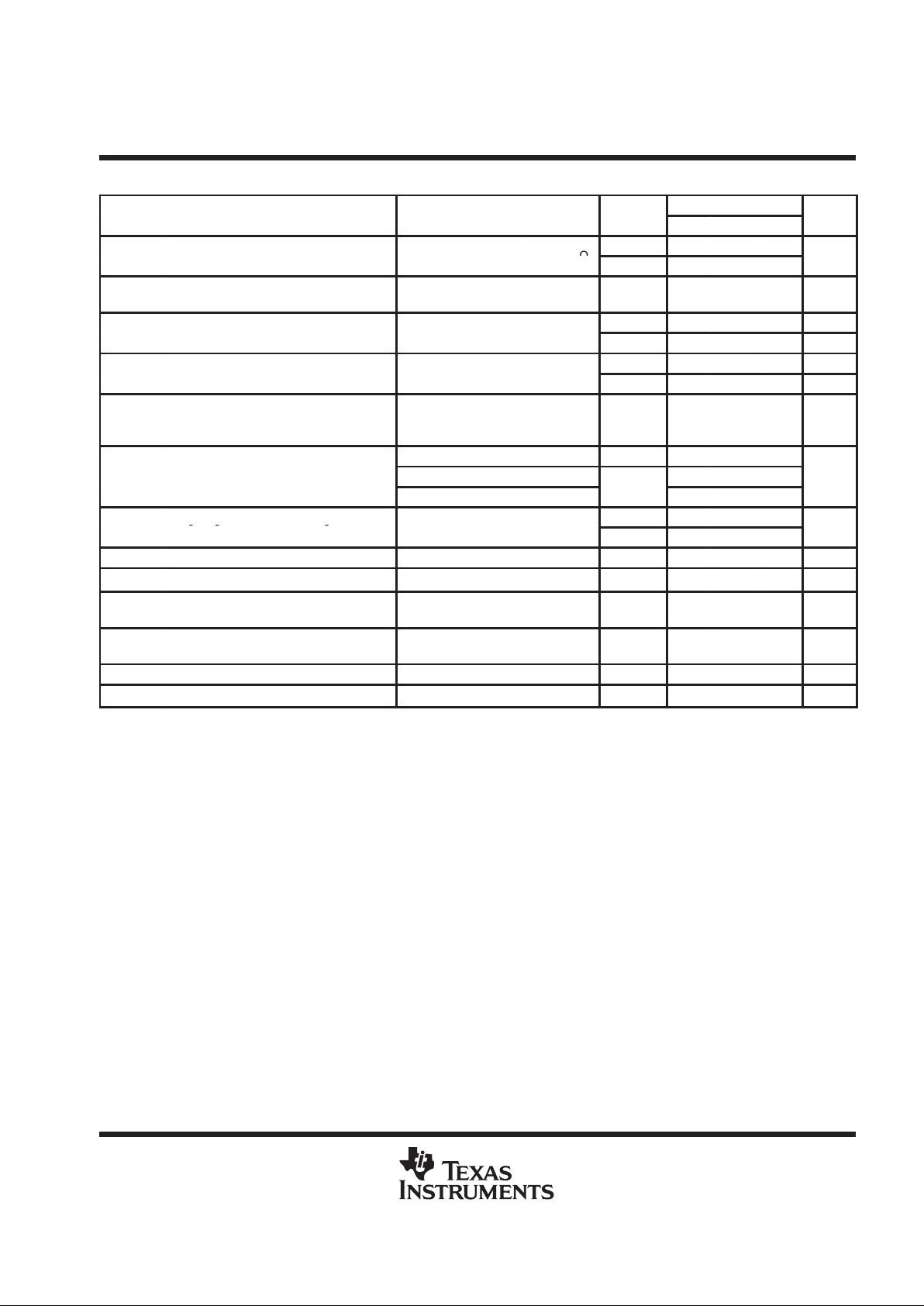
AVAILABLE OPTIONS
PACKAGE
T
A
VIOmax
AT 25°C
SMALL OUTLINE
(D)
PLASTIC DIP
(P)
TSSOP
(PW)
0°C to 70°C 10 mV TL070CD TL070CP TL070CPW
–40°C to 85°C 10 mV TL070ID TL070IP —
–55°C to 125°C 10 mV TL070MD TL070MP —
Copyright 1994, Texas Instruments Incorporated
PRODUCTION DATA information is current as of publication date.
Products conform to specifications per the terms of Texas Instruments
standard warranty. Production processing does not necessarily include
testing of all parameters.
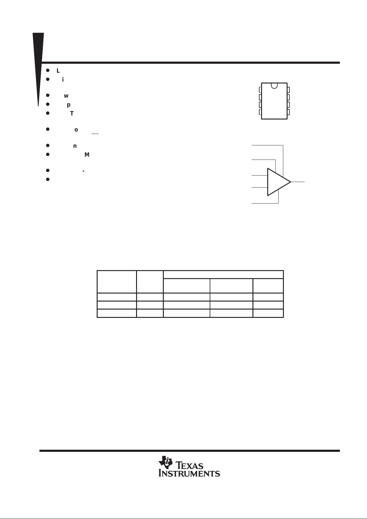
1
2
3
4
8
7
6
5
N1/COMP
IN–
IN+
V
CC –
COMP
V
CC+
OUT
OFFSET N2
D, P, OR PW PACKAGE
(TOP VIEW)
+
–
N1/COMP
COMP
IN+
IN–
OFFSET N2
OUT
symbol
TL070
JFET-INPUT
OPERATIONAL AMPLIFIER
SLOS121A – NOVEMBER 1993 – REVISED AUGUST 1994
2
POST OFFICE BOX 655303 • DALLAS, TEXAS 75265
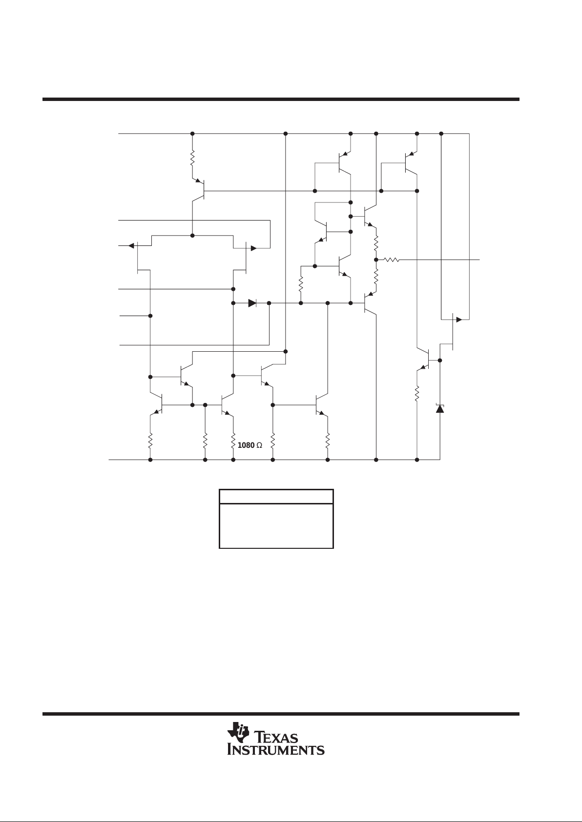
schematic
V
CC+
IN+
OFFSET N2
COMP
V
CC–
1080 Ω
1080 Ω
N1/COMP
IN –
64 Ω
128 Ω
64 Ω
All component values shown are nominal.
OUT
COMPONENT COUNT
†
Transistors
Diodes
Resistors
epi-FET
JFET
13
2
10
1
2
†
Includes all bias and trim circuitry
TL070
JFET-INPUT
OPERATIONAL AMPLIFIER
SLOS121A – NOVEMBER 1993 – REVISED AUGUST 1994
3
POST OFFICE BOX 655303 • DALLAS, TEXAS 75265
absolute maximum ratings over operating free-air temperature range (unless otherwise noted)
†
Supply voltage, V
CC+
(see Note 1) 18 V. . . . . . . . . . . . . . . . . . . . . . . . . . . . . . . . . . . . . . . . . . . . . . . . . . . . . . . . .
Supply voltage, V
CC–
–18 V. . . . . . . . . . . . . . . . . . . . . . . . . . . . . . . . . . . . . . . . . . . . . . . . . . . . . . . . . . . . . . . . . . . .
Differential input voltage, V
ID
(see Note 2) ±30 V. . . . . . . . . . . . . . . . . . . . . . . . . . . . . . . . . . . . . . . . . . . . . . . . . .
Input voltage, V
I
(see Notes 1 and 3) ±15 V. . . . . . . . . . . . . . . . . . . . . . . . . . . . . . . . . . . . . . . . . . . . . . . . . . . . . .
Duration of short-circuit current (see Note 4) unlimited. . . . . . . . . . . . . . . . . . . . . . . . . . . . . . . . . . . . . . . . . . . . .
Continuous total dissipation See Dissipation Rating Table. . . . . . . . . . . . . . . . . . . . . . . . . . . . . . . . . . . . . . . . . . .
Operating free-air temperature range, T
A
: C suffix 0°C to 70°C. . . . . . . . . . . . . . . . . . . . . . . . . . . . . . . . . . . . .
I suffix –40°C to 85°C. . . . . . . . . . . . . . . . . . . . . . . . . . . . . . . . . .
M suffix –55°C to 125°C. . . . . . . . . . . . . . . . . . . . . . . . . . . . . . . . .
Storage temperature range –65°C to 150°C. . . . . . . . . . . . . . . . . . . . . . . . . . . . . . . . . . . . . . . . . . . . . . . . . . . . . .
Lead temperature 1,6 mm (1/16 inch) from case for 10 seconds 260°C. . . . . . . . . . . . . . . . . . . . . . . . . . . . . . .
†
Stresses beyond those listed under “absolute maximum ratings” may cause permanent damage to the device. These are stress ratings only, and
functional operation of the device at these or any other conditions beyond those indicated under “recommended operating conditions” is not
implied. Exposure to absolute-maximum-rated conditions for extended periods may affect device reliability.
NOTES: 1. All voltage values, except differential voltages, are with respect to the midpoint between V
CC +
and V
CC –
.
2. Differential voltages are at IN+ with respect to IN–.
3. The magnitude of the input voltage must never exceed the magnitude of the supply voltage or 15 V, whichever is less.
4. The output may be shorted to ground or to either supply. Temperature and/or supply voltages must be limited to ensure that the
dissipation rating is not exceeded.
DISSIPATION RATING TABLE
PACKAGE
TA ≤ 25°C
POWER RATING
DERATING
FACTOR
DERATE
ABOVE T
A
TA = 70°C
POWER RATING
TA = 85°C
POWER RATING
TA = 125°C
POWER RATING
D 680 mW 5.8 mW/°C 33°C 464 mW 377 mW 145 mW
P 680 mW 8.0 mW/°C65°C 640 mW 520 mW 200 mW
PW 525 mW 4.2 mW/°C 70°C 336 mW N/A N/A
TL070
JFET-INPUT
OPERATIONAL AMPLIFIER
SLOS121A – NOVEMBER 1993 – REVISED AUGUST 1994
4
POST OFFICE BOX 655303 • DALLAS, TEXAS 75265
electrical characteristics, V
CC
±
= ±15 V (unless otherwise noted)
TL070C
PARAMETER
TEST CONDITIONS
T
A
†
MIN TYP MAX
UNIT
p
25°C 3 10
VIOInput offset voltage
V
O
= 0,
R
S
= 50
Ω
Full range 13
mV
α
VIO
Temperature coefficient of input offset
voltage
VO = 0, RS = 50 Ω Full range 18 µV/°C
25°C 5 100 pA
I
IO
I
nput offset curren
t
V
O
=
0
Full range 10 nA
p
25°C 65 200 pA
I
IB
I
nput bias curren
t
‡
V
O
=
0
Full range 7 nA
V
ICR
Common-mode input voltage range 25°C ±11
–12
to
15
V
RL = 10 kΩ
25°C ±12 ±13.5
V
OM
Maimum peak output voltage swing
RL ≥ 10 kΩ
±12
V
RL ≥ 2 kΩ
Full range
±10
Large-signal differential voltage VO = ±10 V ,
25°C 25 200
A
VD
gg g
amplification
O
,
RL ≥ 2 kΩ
Full range 15
V/mV
B
1
Unity-gain bandwidth 25°C 3 MHz
r
i
Input resistance 25°C 10
12
Ω
CMRR Common-mode rejection ratio
VIC = V
ICR
min,
RS = 50 Ω
VO = 0,
25°C 70 100 dB
k
SVR
Supply voltage rejection ratio
(∆V
CC±
/∆VIO)
VCC = ±9 V to ±15 V,
RS = 50 Ω
VO = 0,
25°C 70 100 dB
I
CC
Supply current VO = 0, No load 25°C 1.4 2.5 mA
VO1/V
O2
Crosstalk attenuation AVD = 100 25°C 120 dB
†
All characteristics are measured under open-loop conditions with zero common-mode voltage unless otherwise specified. Full range for TA is
0°C to 70°C.
‡
Input bias currents of a FET-input operational amplifier are normal junction reverse currents, which are temperature sensitive as shown in
Figure 5. Pulse techniques must be used that will maintain the junction temperature as close to the ambient temperature as possible.
TL070
JFET-INPUT
OPERATIONAL AMPLIFIER
SLOS121A – NOVEMBER 1993 – REVISED AUGUST 1994
5
POST OFFICE BOX 655303 • DALLAS, TEXAS 75265
electrical characteristics, V
CC
±
= ±15 V (unless otherwise noted)
TL070I
PARAMETER
TEST CONDITIONS
T
A
†
MIN TYP MAX
UNIT
p
25°C 3 10
VIOInput offset voltage
V
O
= 0,
R
S
= 50
Ω
Full range 13
mV
α
VIO
Temperature coefficient of input offset
voltage
VO = 0, RS = 50 Ω Full range 18 µV/°C
25°C 5 100 pA
I
IO
I
nput offset curren
t
V
O
=
0
Full range 10 nA
p
25°C 65 200 pA
I
IB
I
nput bias curren
t
‡
V
O
=
0
Full range 20 nA
V
ICR
Common-mode input voltage range 25°C ±11
–12
to
15
V
RL = 10 kΩ 25°C ±12 ±13.5
V
OM
Maximum peak output voltage swing
RL ≥ 10 kΩ
±12 V
RL ≥ 2 kΩ
Full range
±10
Large-signal differential voltage V
= ±10 V ,
25°C 25 200
A
VD
gg g
amplification
O
,
RL ≥ 2 kΩ
Full range 15
V/mV
B
1
Unity-gain bandwidth 25°C 3 MHz
r
i
Input resistance 25°C 10
12
Ω
CMRR Common-mode rejection ratio
VIC = V
ICR
min,
RS = 50 Ω
VO = 0,
25°C 70 100 dB
k
SVR
Supply voltage rejection ratio
(∆V
CC±
/∆VIO)
VCC = ±9 V to ±15 V,
RS = 50 Ω
VO = 0
25°C 70 100 dB
I
CC
Supply current VO = 0, No load 25°C 1.4 2.5 mA
VO1/V
O2
Crosstalk attenuation AVD = 100 25°C 120 dB
†
All characteristics are measured under open-loop conditions with zero common-mode voltage unless otherwise specified. Full range for TA is
–40°C to 85°C.
‡
Input bias currents of a FET-input operational amplifier are normal junction reverse currents, which are temperature sensitive as shown in
Figure 5. Pulse techniques must be used that will maintain the junction temperature as close to the ambient temperature as possible.

TL070
JFET-INPUT
OPERATIONAL AMPLIFIER
SLOS121A – NOVEMBER 1993 – REVISED AUGUST 1994
6
POST OFFICE BOX 655303 • DALLAS, TEXAS 75265
electrical characteristics, V
CC
±
= ±15 V (unless otherwise noted)
TL070M
PARAMETER
TEST CONDITIONS
T
A
†
MIN TYP MAX
UNIT
p
25°C 3 10
VIOInput offset voltage
V
O
= 0,
R
S
= 50
Ω
Full range 13
mV
α
VIO
Temperature coefficient of input offset
voltage
VO = 0, RS = 50 Ω Full range 18 µV/°C
25°C 5 100 pA
I
IO
I
nput offset curren
t
V
O
=
0
Full range 20 nA
p
25°C 65 200 pA
I
IB
I
nput bias curren
t
‡
V
O
=
0
Full range 50 nA
V
ICR
Common-mode input voltage range 25°C ±11
–12
to
15
V
RL = 10 kΩ 25°C ±12 ±13.5
V
OM
Maximum peak output voltage swing
RL ≥ 10 kΩ
±12 V
RL ≥ 2 kΩ
Full range
±10
Large-signal differential voltage
25°C 25 200
A
VD
gg g
amplification
V
O
=
±10 V
,
R
L
≥ 2
kΩ
Full range 15
V/mV
B
1
Unity-gain bandwidth 25°C 3 MHz
r
i
Input resistance 25°C 10
12
Ω
CMRR Common-mode rejection ratio
VIC = V
ICR
min,
RS = 50 Ω
VO = 0,
25°C 70 100 dB
k
SVR
Supply voltage rejection ratio
(∆V
CC±
/∆VIO)
VCC = ±9 V to ±15 V,
RS = 50 Ω
VO = 0,
25°C 70 100 dB
I
CC
Supply current VO = 0, No load 25°C 1.4 2.5 mA
VO1/V
O2
Crosstalk attenuation AVD = 100 25°C 120 dB
†
All characteristics are measured under open-loop conditions with zero common-mode voltage unless otherwise specified. Full range for TA is
–55°C to 125°C.
‡
Input bias currents of a FET-input operational amplifier are normal junction reverse currents, which are temperature sensitive as shown in
Figure 5. Pulse techniques must be used that will maintain the junction temperature as close to the ambient temperature as possible.
operating characteristics, V
CC±=
±
15 V, T
A
= 25°C
PARAMETER TEST CONDITIONS MIN TYP MAX UNIT
SR Slew rate at unity gain
VI = 10 V,
CL = 100 pF,
RL = 2 kΩ,
See Figure 1
8 13 V/µs
V
= 20 mV, R
= 2 kΩ,
0.1 µs
trRise time overshoot factor
I
,
CL = 100 pF,
L
,
See Figure 1
20 %
p
f = 1 kHz 18
nV/√Hz
VnEquivalent input noise voltage
R
S
= 20
Ω
f = 10 Hz to 10 kHz 4 µV
I
n
Equivalent input noise current RS = 20 Ω, f = 1 kHz 0.01
pA/√Hz
THD Total harmonic distortion
V
O(rms)
= 10 V,
RL ≥ 2 kΩ,
RS ≤ 1 kΩ,
f = 1 kHz
0.003 %

TL070
JFET-INPUT
OPERATIONAL AMPLIFIER
SLOS121A – NOVEMBER 1993 – REVISED AUGUST 1994
7
POST OFFICE BOX 655303 • DALLAS, TEXAS 75265
PARAMETER MEASUREMENT INFORMATION
Figure 1. Unity-Gain Amplifier
V
I
+
–
CL =
100 pF
RL = 2 kΩ
CC = 18 pF
OUT
Figure 2. Gain-of-10 Inverting Amplifier
V
I
+
–
10 kΩ
1 kΩ
R
L
CL = 100 pF
OUT
Figure 3. Feed-Forward Compensation
C2
C1
+
–
100 kΩ
N1
500 pF
IN–
OUT
Figure 4. Input Offset Voltage Null Circuit
N1
+
–
2 MΩ
N2
COMP
1 MΩ
V
CC+
IN–
IN+
OUT

TL070
JFET-INPUT
OPERATIONAL AMPLIFIER
SLOS121A – NOVEMBER 1993 – REVISED AUGUST 1994
8
POST OFFICE BOX 655303 • DALLAS, TEXAS 75265
TYPICAL CHARACTERISTICS
Table of Graphs
FIGURE
I
IB
Input bias current vs Free-air temperature 5
vs Frequenc
y
6, 7, 8
p
vs Frequency
vs Free-air temperature
6, 7, 8
9
VOMMaximum output voltage
vs Load resistance 10
vs Supply voltage 11
p
vs Free-air temperature 12
AVDLarge-signal differential voltage amplification
vs Frequency 14
A
VD
Differential voltage amplification vs Frequency 13
Phase shift vs Frequency 14
Normalized unity-gain bandwidth vs Free-air temperature 15
Normalized phase shift vs Free-air temperature 15
CMRR Common-mode rejection ratio vs Free-air temperature 16
pp
I
Supply current
vs Su ly voltage
17
ICCSu ly current
vs Free-air temperature
18
P
D
Total power dissipation vs Free-air temperature 19
Normalized slew rate vs Free-air temperature 20
V
n
Equivalent input noise voltage vs Frequency 21
THD Total harmonic distortion vs Frequency 22
Large-signal pulse response vs Time 23
V
O
Output voltage vs Elapsed time 24

TL070
JFET-INPUT
OPERATIONAL AMPLIFIER
SLOS121A – NOVEMBER 1993 – REVISED AUGUST 1994
9
POST OFFICE BOX 655303 • DALLAS, TEXAS 75265
TYPICAL CHARACTERISTICS
†
Figure 5
IIB– Input Bias Current – nA
TA – Free-Air Temperature – °C
INPUT BIAS CURRENT
vs
FREE-AIR TEMPERATURE
IB
I
10
1
0.1
0.01
100
–75 – 50 –25 0 25 50 75 100 125
V
CC±
= ±15 V
Figure 6
±15
±12.5
±10
±7.5
±5
±2.5
0
VOM – Maximum Peak Output Voltage – V
f – Frequency – Hz
100 1 k 10 k 100 k 1 M 10 M
MAXIMUM PEAK OUTPUT VOLTAGE
vs
FREQUENCY
V
OM
V
CC±
= ±10 V
V
CC±
= ±15 V
V
CC±
= ±5 V
RL = 2 kΩ
TA = 25°C
See Figure 2
Figure 7
10 M1 M100 k10 k1 k100
f – Frequency – Hz
VOM – Maximum Peak Output Voltage – V
0
±2.5
±5
±7.5
±10
±12.5
±15
TA = 25°C
RL = 2 kΩ
V
CC±
= ±10 V
V
CC±
= ±5 V
MAXIMUM PEAK OUTPUT VOLTAGE
vs
FREQUENCY
V
OM
V
CC±
= ±15 V
See Figure 2
Figure 8
0
±2.5
±5
±7.5
±10
±12.5
±15
10 k 40 k 100 k 400 k 1 M 4 M 10 M
f – Frequency – Hz
MAXIMUM PEAK OUTPUT VOLTAGE
vs
FREQUENCY
VOM – Maximum Peak Output Voltage – V
V
OM
V
CC±
= ±15 V
RL = 2 kΩ
See Figure 2
TA = –55°C
TA = 25°C
TA = 125°C
†
Data at high and low temperatures are applicable only within the rated operating free-air temperature ranges of the various devices. An 18-pF
compensation capacitor is used.

TL070
JFET-INPUT
OPERATIONAL AMPLIFIER
SLOS121A – NOVEMBER 1993 – REVISED AUGUST 1994
10
POST OFFICE BOX 655303 • DALLAS, TEXAS 75265
TYPICAL CHARACTERISTICS
†
Figure 9
–75
0
VOM – Maximum Peak Output Voltage – V
TA – Free-Air Temperature – °C
125
±15
–50 –25 0 25 50 75 100
±2.5
±5
±7.5
±10
±12.5
RL = 10 kΩ
V
CC±
= ±15 V
See Figure 2
MAXIMUM PEAK OUTPUT VOLTAGE
vs
FREE-AIR TEMPERATURE
ÁÁ
V
OM
RL = 2 kΩ
Figure 10
0.1
0
RL – Load Resistance – kΩ
10
±15
±2.5
±5
±7.5
±10
±12.5
V
CC±
= ±15 V
TA = 25°C
See Figure 2
0.2 0.4 0.7 1 2 4 7
MAXIMUM PEAK OUTPUT VOLTAGE
vs
LOAD RESISTANCE
VOM – Maximum Peak Output Voltage – V
V
OM
Figure 11
0
0
VOM – Maximum Peak Output Voltage – V
|V
CC±
| – Supply Voltage – V
16
±15
2 4 6 8 10 12 14
±2.5
±5
±7.5
±10
±12.5
RL = 10 kΩ
TA = 25°C
MAXIMUM PEAK OUTPUT VOLTAGE
vs
SUPPLY VOLTAGE
V
OM
Figure 12
–75
1
TA – Free-Air Temperature – °C
125
1000
–50 –25 0 25 50 75 100
2
4
10
20
40
100
200
400
V
CC±
= ±15 V
VO = ±10 V
RL = 2 kΩ
LARGE-SIGNAL
DIFFERENTIAL VOLTAGE AMPLIFICATION
VS
FREE-AIR TEMPERATURE
– Large-Signal Differential Voltage Amplification – V/mV
A
VD
†
Data at high and low temperatures are applicable only within the rated operating free-air temperature ranges of the various devices. An 18-pF
compensation capacitor is used.

TL070
JFET-INPUT
OPERATIONAL AMPLIFIER
SLOS121A – NOVEMBER 1993 – REVISED AUGUST 1994
11
POST OFFICE BOX 655303 • DALLAS, TEXAS 75265
TYPICAL CHARACTERISTICS
†
Figure 13
100
1
f – Frequency – Hz
10 M
10
6
1 k 10 k 100 k 1 M
10
1
10
2
10
3
10
4
10
5
DIFFERENTIAL VOLTAGE AMPLIFICATION
vs
FREQUENCY WITH FEED-FORWARD
COMPENSATION
V
CC±
= ±15 V
C2 = 3 pF
TA = 25°C
See Figure 3
AVD – Differential Voltage Amplification – dB
A
VD
Figure 14
0°
45°
180
°
135
°
90°
1
1
f – Frequency – Hz
10 M
10
6
10 100 1 k 10 k 100 k 1 M
10
1
10
2
10
3
10
4
10
5
Differential
Voltage
Amplification
(left scale)
V
CC±
= ±5 V to ±15 V
RL = 2 kΩ
TA = 25°C
Phase Shift
(right scale)
LARGE-SIGNAL
DIFFERENTIAL VOLTAGE AMPLIFICATION
AND PHASE SHIFT
vs
FREQUENCY
– Large-Signal Differential Voltage Amplification – dB
A
VD
Figure 15
1
–75
0.7
Normalized Unity-Gain Bandwidth
TA – Free-Air Temperature – °C
125
1.3
–50 –25 0 25 50 75 100
0.8
0.9
1
1.1
1.2
Unity-Gain Bandwidth
(left scale)
V
CC±
= ±15 V
RL = 2 kΩ
f = B1 for Phase Shift
NORMALIZED UNITY-GAIN BANDWIDTH
AND PHASE SHIFT
vs
FREE-AIR TEMPERATURE
Normalized Phase Shift
Phase
Shift
(right scale)
1.02
1.01
0.99
0.98
1.03
0.97
Figure 16
–75
83
CMRR – Common-Mode Rejection Ratio – dB
TA – Free-Air Temperature – °C
125
89
–50 –25 0 25 50 75 100
84
85
86
87
88
V
CC±
= ±15 V
RL = 10 kΩ
COMMO
N-MODE REJECTION RATI
O
vs
FREE-AIR TEMPERATURE
†
Data at high and low temperatures are applicable only within the rated operating free-air temperature ranges of the various devices. An 18-pF
compensation capacitor is used.

TL070
JFET-INPUT
OPERATIONAL AMPLIFIER
SLOS121A – NOVEMBER 1993 – REVISED AUGUST 1994
12
POST OFFICE BOX 655303 • DALLAS, TEXAS 75265
TYPICAL CHARACTERISTICS
†
Figure 17
0
0
ICC – Supply Current – mA
|V
CC±
| – Supply Voltage – V
16
2
2 4 6 8 10 12 14
0.2
0.4
0.6
0.8
1
1.2
1.4
1.6
1.8
TA = 25°C
No Signal
No Load
SUPPLY CURRENT
vs
SUPPLY VOLTAGE
CC ±
I
Figure 18
–75
0
TA – Free-Air Temperature – °C
125
2
–50 –25 0 25 50 75 100
0.2
0.4
0.6
0.8
1
1.2
1.4
1.6
1.8
SUPPLY CURRENT
vs
FREE-AIR TEMPERATURE
ICC – Supply Current – mA
CC ±
I
V
CC±
= ±15 V
No Signal
No Load
Figure 19
–75
0
PD – Total Power Dissipated – mW
TA – Free-Air Temperature – °C
125
–50 –25 0 25 50 75 100
25
50
75
100
TOTAL POWER DISSIPATED
vs
FREE-AIR TEMPERATURE
P
D
V
CC±
= ±15 V
No Signal
No Load
Figure 20
–75
0.85
Normalized Slew Rate
TA – Free-Air Temperature – °C
125
1.15
–50 – 25 0 25 50 75 100
0.90
0.95
1
1.05
1.10
NORMALIZED SLEW RATE
vs
FREE-AIR TEMPERATURE
V
CC±
= ±15 V
RL = 2 kΩ
CL = 100 pF
†
Data at high and low temperatures are applicable only within the rated operating free-air temperature ranges of the various devices. An 18-pF
compensation capacitor is used.

TL070
JFET-INPUT
OPERATIONAL AMPLIFIER
SLOS121A – NOVEMBER 1993 – REVISED AUGUST 1994
13
POST OFFICE BOX 655303 • DALLAS, TEXAS 75265
TYPICAL CHARACTERISTICS
Figure 21
10
0
Vn – Equivalent Input Noise Voltage – nV/Hz
f – Frequency – Hz
100 k
50
10
20
30
40
V
CC±
= ±15 V
AVD = 10
RS = 20 Ω
TA = 25°C
40 100 400 1 k 4 k 10 k 40 k
EQUIVALENT INPUT NOISE VOLTAGE
vs
FREQUENCY
nV/ Hz
V
n
Figure 22
0.001
THD – Total Harmonic Distortion – %
1
40 k10 k4 k1 k400 100 k
f – Frequency – Hz
100
0.004
0.01
0.04
0.1
0.4
TOTAL HARMONIC DISTORTION
vs
FREQUENCY
T
HD
V
CC±
= ±15 V
AVD = 1
VI
(RMS)
= 6 V
TA = 25°C
Figure 23
–6
t – Time – µs
3.5
6
0
0.5 1 1.5 2 2.5 3
–4
–2
0
2
4
Output
Input
V
CC±
= ±15 V
RL = 2 kΩ
CL = 100 pF
TA = 25°C
VOLTAGE-FOLLOWER
LARGE-SIGNAL PULSE RESPONSE
– Input and Output Voltage – V
V
O
V
I
and
Figure 24
10%
–4
VO – Output Voltage – mV
t – Elasped Time – µs
0.7
28
0 0.1 0.2 0.3 0.4 0.5 0.6
0
4
8
12
16
20
24
V
CC±
= ±15 V
RL = 2 kΩ
TA = 25°C
t
r
Overshoot
90%
OUTPUT VOLTAGE
vs
ELAPSED TIME
V
O

TL070
JFET-INPUT
OPERATIONAL AMPLIFIER
SLOS121A – NOVEMBER 1993 – REVISED AUGUST 1994
14
POST OFFICE BOX 655303 • DALLAS, TEXAS 75265
APPLICATION INFORMATION
75 µF
100 Ω
100 Ω
Input
Output
68 kΩ
MIN
100 kΩ
Treble
MAX
0.003 µF
0.003 µF
3.3 kΩ10 kΩ
0.03 µF
MAX
Bass
100 kΩ
MIN
10 kΩ
10 kΩ
0.03 µF
+
47 µF
Gain
5 kΩ
+
–
10 pF
V
CC+
V
CC–
V
CC–
V
CC+
220 kΩ
0.00375 µF
0.01 µF
1
µF
27 kΩ
10 pF
47 kΩ
50 pF
Balance
+
–
+
TL070
TL070
Figure 25. IC Preamplifier
MIN Bass
20
–25
Voltage Amplification – dB
f – Frequency – Hz
20 k
25
–20
–15
–10
–5
0
5
10
15
20
V
CC±
= ±15 V
TA = 25°C
See Figure 25
MAX Bass
40 100 200 400 1 k 2 k 4 k 10 k
IC PREAMPLIFIER
RESPONSE CHARACTERISTICS
MIN
Treble
MAX
Treble
Figure 26

IMPORTANT NOTICE
T exas Instruments and its subsidiaries (TI) reserve the right to make changes to their products or to discontinue
any product or service without notice, and advise customers to obtain the latest version of relevant information
to verify, before placing orders, that information being relied on is current and complete. All products are sold
subject to the terms and conditions of sale supplied at the time of order acknowledgement, including those
pertaining to warranty, patent infringement, and limitation of liability.
TI warrants performance of its semiconductor products to the specifications applicable at the time of sale in
accordance with TI’s standard warranty. Testing and other quality control techniques are utilized to the extent
TI deems necessary to support this warranty. Specific testing of all parameters of each device is not necessarily
performed, except those mandated by government requirements.
CERT AIN APPLICATIONS USING SEMICONDUCTOR PRODUCTS MAY INVOLVE POTENTIAL RISKS OF
DEATH, PERSONAL INJURY, OR SEVERE PROPERTY OR ENVIRONMENTAL DAMAGE (“CRITICAL
APPLICATIONS”). TI SEMICONDUCTOR PRODUCTS ARE NOT DESIGNED, AUTHORIZED, OR
WARRANTED TO BE SUITABLE FOR USE IN LIFE-SUPPORT DEVICES OR SYSTEMS OR OTHER
CRITICAL APPLICATIONS. INCLUSION OF TI PRODUCTS IN SUCH APPLICA TIONS IS UNDERST OOD TO
BE FULLY AT THE CUSTOMER’S RISK.
In order to minimize risks associated with the customer’s applications, adequate design and operating
safeguards must be provided by the customer to minimize inherent or procedural hazards.
TI assumes no liability for applications assistance or customer product design. TI does not warrant or represent
that any license, either express or implied, is granted under any patent right, copyright, mask work right, or other
intellectual property right of TI covering or relating to any combination, machine, or process in which such
semiconductor products or services might be or are used. TI’s publication of information regarding any third
party’s products or services does not constitute TI’s approval, warranty or endorsement thereof.
Copyright 1998, Texas Instruments Incorporated
 Loading...