

TL061, TL061A, TL061B, TL061Y, TL062, TL062A
TL062B, TL062Y, TL064, TL064A, TL064B, TL064Y
LOW-POWER JFET-INPUT OPERATIONAL AMPLIFIERS
SLOS078F – NOVEMBER 1978 – REVISED JANUARY 1999
1
POST OFFICE BOX 655303 • DALLAS, TEXAS 75265
D
Very Low Power Consumption
D
Typical Supply Current...200 µA
(Per Amplifier)
D
Wide Common-Mode and Differential
Voltage Ranges
D
Low Input Bias and Offset Currents
D
Common-Mode Input Voltage Range
Includes V
CC+
D
Output Short-Circuit Protection
D
High Input Impedance...JFET-Input Stage
D
Internal Frequency Compensation
D
Latch-Up-Free Operation
D
High Slew Rate...3.5 V/µs Typ
description
The JFET-input operational amplifiers of the
TL06_ series are designed as low-power versions
of the TL08_ series amplifiers. They feature high
input impedance, wide bandwidth, high slew rate,
and low input offset and input bias currents. The
TL06_ series feature the same terminal
assignments as the TL07_ and TL08_ series.
Each of these JFET-input operational amplifiers
incorporates well-matched, high-voltage JFET
and bipolar transistors in a monolithic integrated
circuit.
The C-suffix devices are characterized for
operation from 0°C to 70°C. The I-suffix devices
are characterized for operation from –40°C to
85°C, and the M-suffix devices are characterized
for operation over the full military temperature
range of –55°C to 125°C.
Please be aware that an important notice concerning availability, standard warranty, and use in critical applications of
Texas Instruments semiconductor products and disclaimers thereto appears at the end of this data sheet.
Copyright 1999, Texas Instruments Incorporated
PRODUCTION DATA information is current as of publication date.
Products conform to specifications per the terms of Texas Instruments
standard warranty. Production processing does not necessarily include
testing of all parameters.
1
2
3
4
8
7
6
5
OFFSET N1
IN–
IN+
V
CC–
NC
V
CC+
OUT
OFFSET N2
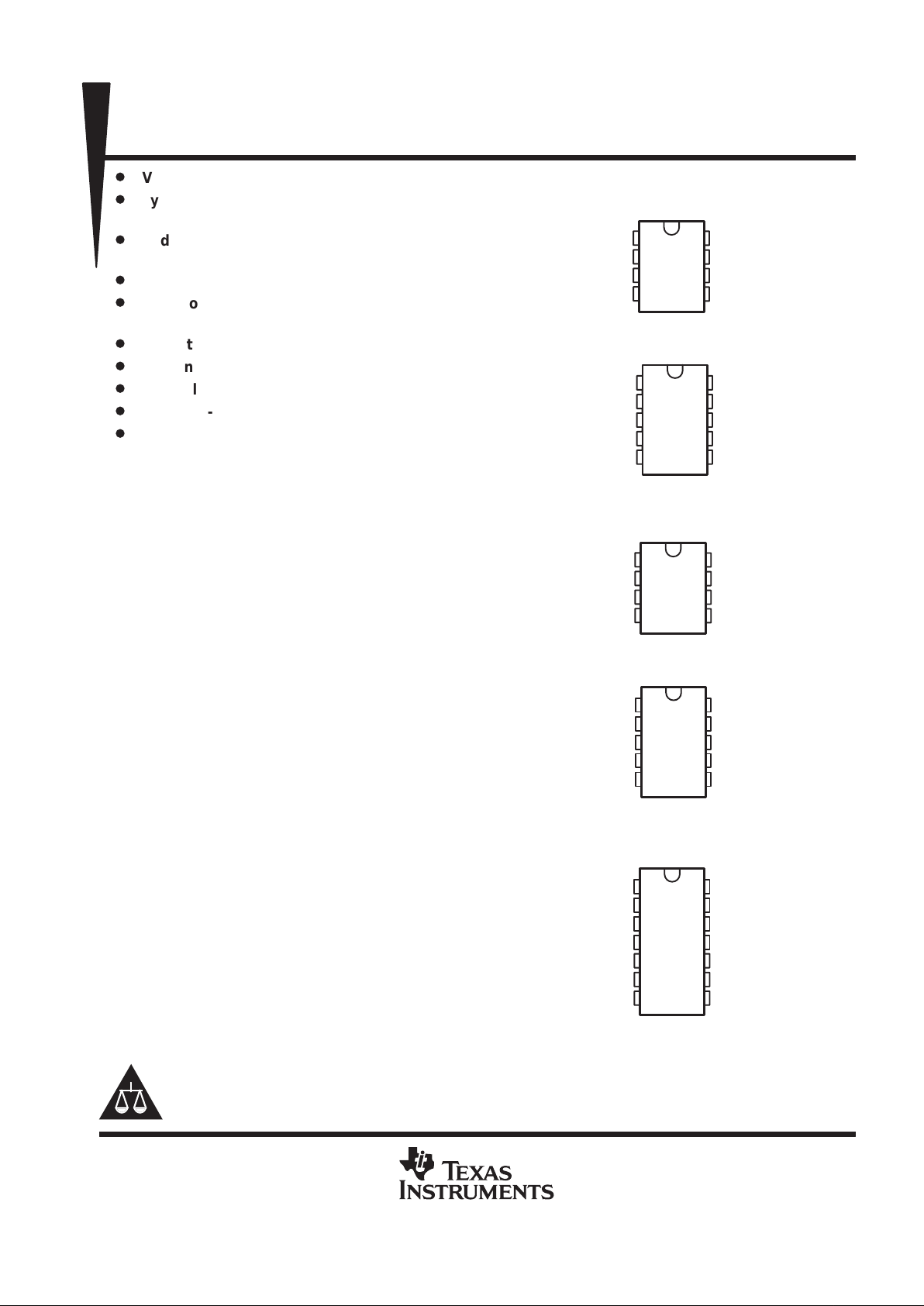
TL061, TL061A, TL061B
D, JG, P, OR PW PACKAGE
(TOP VIEW)
1
2
3
4
8
7
6
5
1OUT
1IN–
1IN+
V
CC–
V
CC+
2OUT
2IN–
2IN+
TL062, TL062A, TL062B
D, JG, P, OR PW PACKAGE
(TOP VIEW)
1
2
3
4
5
10
9
8
7
6
NC
OFFSET N1
IN–
IN+
V
CC–
NC
NC
V
CC+
OUT
OFFSET N2
TL061 ...U PACKAGE
(TOP VIEW)
1
2
3
4
5
6
7
14
13
12
11
10
9
8
1OUT
1IN–
1IN+
V
CC+
2IN+
2IN–
2OUT
4OUT
4IN–
4IN+
V
CC–
3IN+
3IN–
3OUT
TL064 . . . D, J, N, PW, OR W PACKAGE
TL064A, TL064B ...D OR N PACKAGE
(TOP VIEW)
•
1
2
3
4
5
10
9
8
7
6
NC
1OUT
1IN–
1IN+
V
CC–
NC
V
CC+
2OUT
2IN–
2IN+
TL062 ...U PACKAGE
(TOP VIEW)
•
NC – No internal connection
TL061, TL061A, TL061B, TL061Y, TL062, TL062A
TL062B, TL062Y, TL064, TL064A, TL064B, TL064Y
LOW-POWER JFET-INPUT OPERATIONAL AMPLIFIERS
SLOS078F – NOVEMBER 1978 – REVISED JANUARY 1999
2
POST OFFICE BOX 655303 • DALLAS, TEXAS 75265
NC
2OUT
NC
2IN–
NC
3212019
910111213
4
5
6
7
8
18
17
16
15
14
NC
V
CC+
NC
OUT
NC
NC
IN–
NC
IN+
NC
TL061 ...FK PACKAGE
(TOP VIEW)
NC
OFFSET N1
NC
OFFSET N2
NC
NC
NC
NC
NC
3212019
910111213
4
5
6
7
8
18
17
16
15
14
4IN+
NC
V
CC–
NC
3IN+
1IN+
NC
V
CC+
NC
2IN+
1IN–
1OUT
NC
3OUT
3IN–
4OUT
4IN–
2IN–
2OUT
NC
3 2 1 20 19
910111213
4
5
6
7
8
18
17
16
15
14
NC
1IN–
NC
1IN+
NC
TL062 . . . FK PACKAGE
(TOP VIEW)
NC
1OUT
NC
2IN+
NC
NC
NC
NC
V
CC–
V
CC+
TL064 . . . FK PACKAGE
(TOP VIEW)
NC – No internal connection
V
CC–
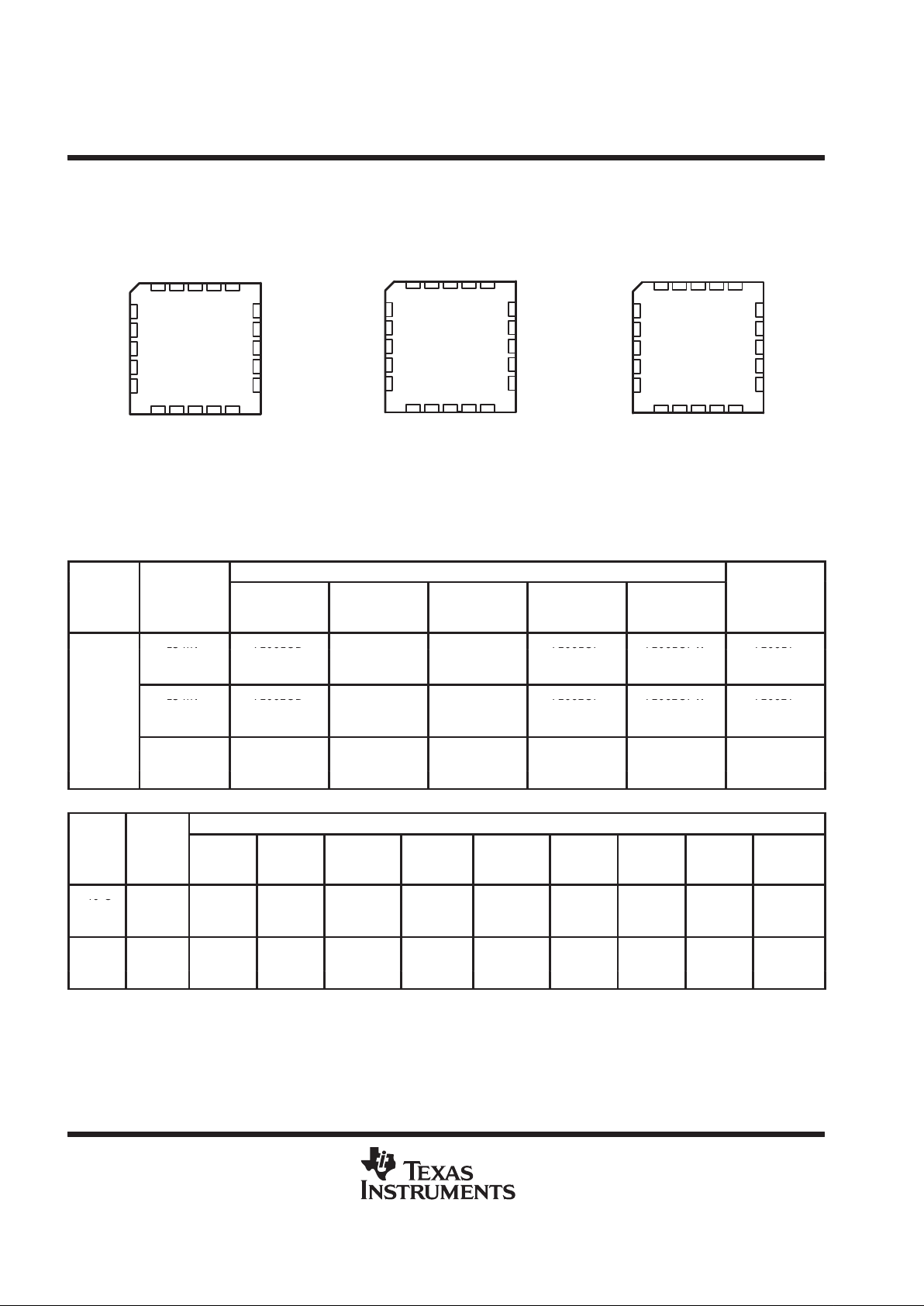
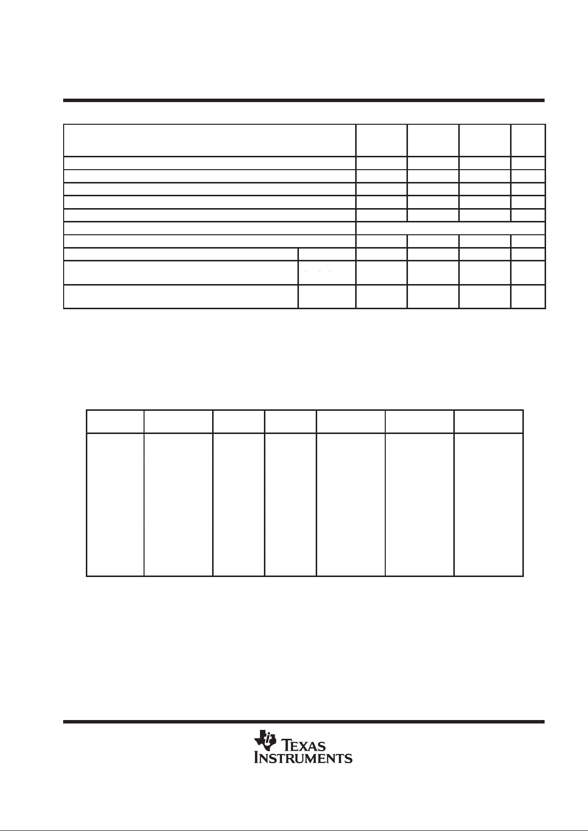
AVAILABLE OPTIONS
PACKAGED DEVICES
T
A
VIOMAX
AT 25°C
SMALL
OUTLINE
(D008)
†
SMALL
OUTLINE
(D014)
†
PLASTIC
DIP
(N)
PLASTIC
DIP
(P)
TSSOP
(PW)
CHIP FORM
(Y)
15 mV TL061CD TL061CP TL061CPW TL061Y
15 mV
6 mV
TL061CD
TL061ACD
TL061CP
TL061ACP
TL061CPW
TL061Y
3 mV TL061BCD TL061BCP
0°C
15 mV TL062CD TL062CP TL062CPW TL062Y
to
15 mV
6 mV
TL062CD
TL062ACD
TL062CP
TL062ACP
TL062CPW
TL062Y
70°C
3 mV TL062BCD TL062BCP
15 mV TL064CD TL064CN TL064CPW TL064Y
6 mV TL064ACD TL064ACN
3 mV TL064BCD TL064BCN
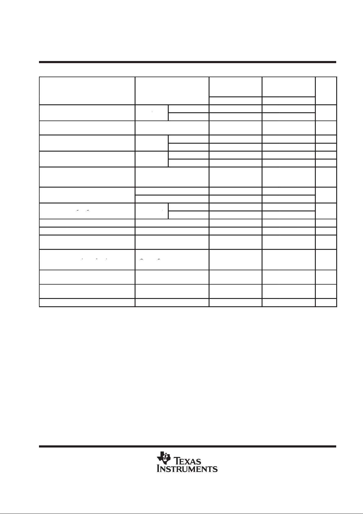
PACKAGE
T
A
VIOMAX
AT 25°C
SMALL
OUTLINE
(D008)
†
SMALL
OUTLINE
(D014)
†
CHIP
CARRIER
(FK)
CERAMIC
DIP
(J)
CERAMIC
DIP
(JG)
PLASTIC
DIP
(N)
PLASTIC
DIP
(P)
FLAT
PACK
(U)
FLAT
PACK
(W)
–40°C
40 C
to
6 mV
TL061ID
TL064ID TL064IN
TL061IP
85°C
TL062ID
TL062IP
–55°C 6 mV TL061MFK TL061MJG TL061MU
to 6 mV TL062MFK TL062MJG TL062MU
125°C 9 mV TL064MFK TL064MJ TL064MW
†
The D package is available taped and reeled. Add the suffix R to the device type (e.g., TL061CDR).
TL061, TL061A, TL061B, TL061Y, TL062, TL062A
TL062B, TL062Y, TL064, TL064A, TL064B, TL064Y
LOW-POWER JFET-INPUT OPERATIONAL AMPLIFIERS
SLOS078F – NOVEMBER 1978 – REVISED JANUARY 1999
3
POST OFFICE BOX 655303 • DALLAS, TEXAS 75265
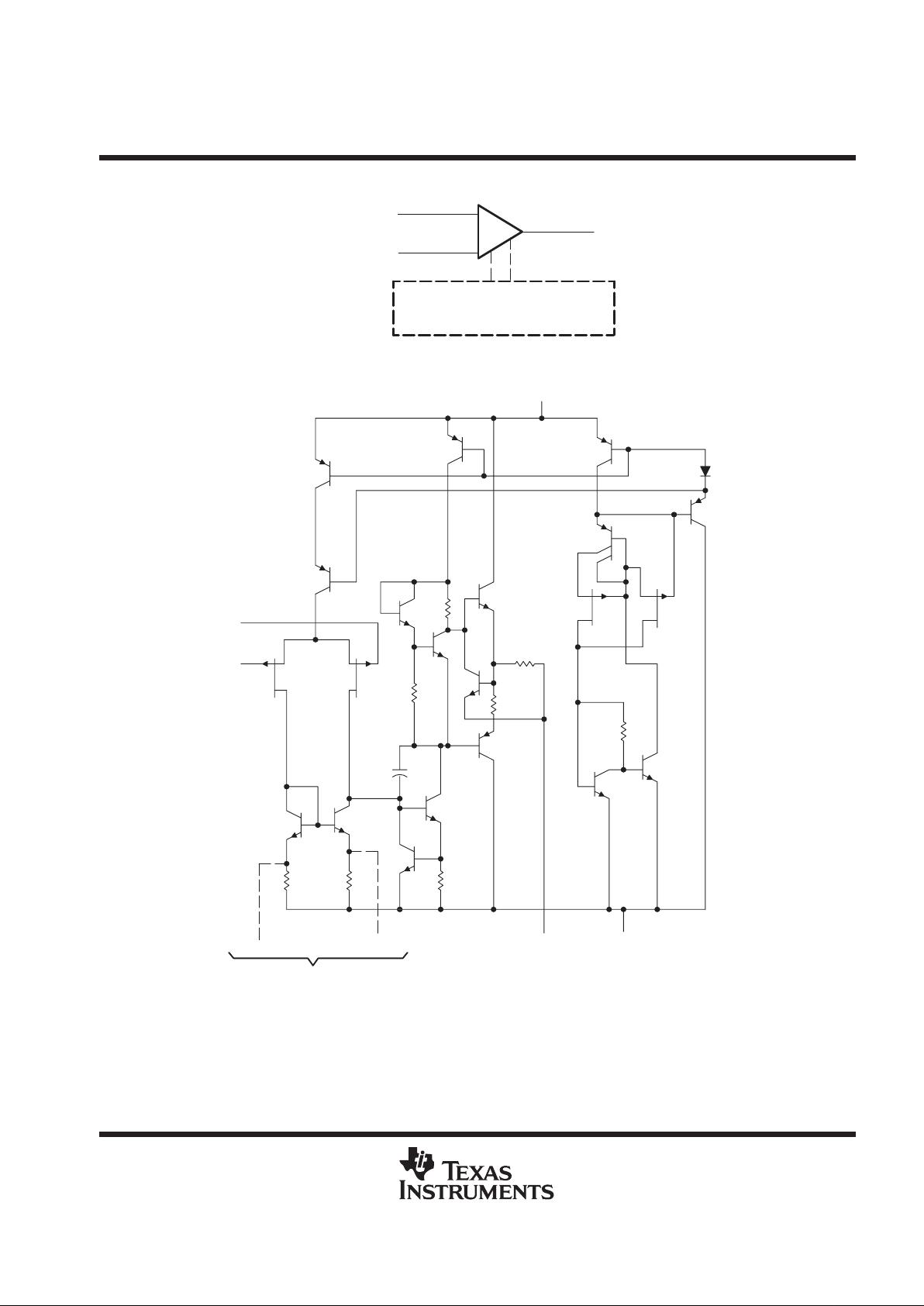
symbol (each amplifier)
+
–
IN+
IN–
OUT
OFFSET N1
Offset Null/Compensation
TL061 Only
OFFSET N2
schematic (each amplifier)
IN+
50 Ω
100 Ω
C1
V
CC+
OUT V
CC–
OFFSET N1
TL061 Only
OFFSET N2
IN–
C1 = 10 pF on TL061, TL062, and TL064
Component values shown are nominal.
TL061, TL061A, TL061B, TL061Y, TL062, TL062A
TL062B, TL062Y, TL064, TL064A, TL064B, TL064Y
LOW-POWER JFET-INPUT OPERATIONAL AMPLIFIERS
SLOS078F – NOVEMBER 1978 – REVISED JANUARY 1999
4
POST OFFICE BOX 655303 • DALLAS, TEXAS 75265
TL061Y chip information
This chip, when properly assembled, has characteristics similar to the TL061. Thermal compression or
ultrasonic bonding can be used on the doped-aluminum bonding pads. The chips can be mounted with
conductive epoxy or a gold-silicon preform.
Bonding-Pad Assignments
+
–
OUT
IN+
IN–
V
CC+
(7)
(3)
(2)
(6)
(4)
V
CC–
(1)
(5)
OFFSET N1
OFFSET N2
Chip Thickness: 15 Mils Typical
Bonding Pads: 4 × 4 Mils Minimum
TJ(max) = 150°C
Tolerances Are ±10%.
All Dimensions Are in Mils.
Pin (4) is Internally Connected
to Backside of Chip.
41
53
(6)
(7)
(8)
(1) (2)
(3)
(4)(5)
TL061, TL061A, TL061B, TL061Y, TL062, TL062A
TL062B, TL062Y, TL064, TL064A, TL064B, TL064Y
LOW-POWER JFET-INPUT OPERATIONAL AMPLIFIERS
SLOS078F – NOVEMBER 1978 – REVISED JANUARY 1999
5
POST OFFICE BOX 655303 • DALLAS, TEXAS 75265
TL062Y chip information
This chip, when properly assembled, has characteristics similar to the TL062. Thermal compression or
ultrasonic bonding can be used on the doped-aluminum bonding pads. The chips can be mounted with
conductive epoxy or a gold-silicon preform.
Bonding-Pad Assignments
Chip Thickness: 15 Mils Typical
Bonding Pads: 4 × 4 Mils Minimum
TJ(max) = 150°C
Tolerances Are ±10%.
All Dimensions Are in Mils.
Pin (4) is Internally Connected to Backside of Chip.
+
–
1OUT
1IN+
1IN–
V
CC+
(8)
(6)
(3)
(2)
(5)
(1)
–
+
(7)
2IN+
2IN–
2OUT
(4)
V
CC–
66
49
(6) (5)
(4)
(3)(2)(1)
(8)
(7)
TL061, TL061A, TL061B, TL061Y, TL062, TL062A
TL062B, TL062Y, TL064, TL064A, TL064B, TL064Y
LOW-POWER JFET-INPUT OPERATIONAL AMPLIFIERS
SLOS078F – NOVEMBER 1978 – REVISED JANUARY 1999
6
POST OFFICE BOX 655303 • DALLAS, TEXAS 75265
TL064Y chip information
This chip, when properly assembled, has characteristics similar to the TL064. Thermal compression or
ultrasonic bonding can be used on the doped-aluminum bonding pads. The chips can be mounted with
conductive epoxy or a gold-silicon preform.
Bonding-Pad Assignments
Chip Thickness: 15 Mils Typical
Bonding Pads: 4 × 4 Mils Minimum
TJ(max) = 150°C
Tolerances Are ±10%.
All Dimensions Are in Mils.
Pin (11) is Internally Connected
to Backside of Chip.
+
–
1OUT
1IN+
1IN–
V
CC+
(4)
(6)
(3)
(2)
(5)
(1)
–
+
(7)
2IN+
2IN–
2OUT
(11)
V
CC–
+
–
4OUT
4IN+
4IN–
(13)
(10)
(9)
(12)
(8)
–
+
(14)
3OUT
3IN+
3IN–
60
110
(13)
(14)
(1)
(2)
(3) (5) (6)
(7)
(8)
(9)
(10)
(12)
(11)
(4)
TL061, TL061A, TL061B, TL061Y, TL062, TL062A
TL062B, TL062Y, TL064, TL064A, TL064B, TL064Y
LOW-POWER JFET-INPUT OPERATIONAL AMPLIFIERS
SLOS078F – NOVEMBER 1978 – REVISED JANUARY 1999
7
POST OFFICE BOX 655303 • DALLAS, TEXAS 75265
absolute maximum ratings over operating free-air temperature range (unless otherwise noted)
†
TL06_C
TL06_AC
TL06_BC
TL06_I TL06_M UNIT
Supply voltage, V
CC+
(see Note 1) 18 18 18 V
Supply voltage, V
CC–
(see Note 1) –18 –18 –18 V
Differential input voltage, VID (see Note 2) ±30 ±30 ±30 V
Input voltage, VI (see Notes 1 and 3) ±15 ±15 ±15 V
Duration of output short circuit (see Note 4) unlimited unlimited unlimited
Continuous total dissipation See Dissipation Rating Table
Storage temperature range, T
stg
–65 to 150 –65 to 150 –65 to 150 °C
Case temperature for 60 seconds FK package 260 °C
p
J, JG, U, or
°
Lead temperature 1,6 mm (1/16 inch) from case for 60 seconds
,,,
W package
300
°C
p
D, N, P, or
°
Lead temperature 1,6 mm (1/6 inch) from case for 10 seconds
PW package
260
260
°C
†
Stresses beyond those listed under “absolute maximum ratings” may cause permanent damage to the device. These are stress ratings only, and
functional operation of the device at these or any other conditions beyond those indicated under “recommended operating conditions” is not
implied. Exposure to absolute-maximum-rated conditions for extended periods may affect device reliability.
NOTES: 1. All voltage values except differential voltages are with respect to the midpoint between V
CC+
and V
CC–
.
2. Differential voltages are at IN+ with respect to IN–.
3. The magnitude of the input voltage must never exceed the magnitude of the supply voltage or 15 V, whichever is less.
4. The output may be shorted to ground or to either supply. Temperature and/or supply voltages must be limited to ensure that the
dissipation rating is not exceeded.
DISSIPATION RATING TABLE
PACKAGE
TA ≤ 25°C
POWER RATING
DERATING
FACTOR
DERATE
ABOVE T
A
TA = 70°C
POWER RATING
TA = 85°C
POWER RATING
TA = 125°C
POWER RATING
D (8 pin) 680 mW 5.8 mW/°C 33°C 465 mW 378 mW N/A
D (14 pin) 680 mW 7.6 mW/°C 60°C 604 mW 490 mW N/A
FK 680 mW 1 1.0 mW/°C 88°C 680 mW 680 mW 273 mW
J 680 mW 1 1.0 mW/°C 88°C 680 mW 680 mW 273 mW
JG 680 mW 8.4 mW/°C 69°C 672 mW 546 mW 210 mW
N 680 mW 9.2 mW/°C 76°C 680 mW 597 mW N/A
P 680 mW 8.0 mW/°C 65°C 640 mW 520 mW N/A
PW (8 pin) 525 mW 4.2 mW/°C 25°C 336 mW N/A N/A
PW (14 pin) 700 mW 5.6 mW/°C 25°C 448 mW N/A N/A
U 675 mW 5.4 mW/°C 25°C 432 mW 351 mW 135 mW
W 680 mW 8.0 mW/°C 65°C 640 mW 520 mW 200 mW

TL061, TL061A, TL061B, TL061Y, TL062, TL062A
TL062B, TL062Y, TL064, TL064A, TL064B, TL064Y
LOW-POWER JFET-INPUT OPERATIONAL AMPLIFIERS
SLOS078F – NOVEMBER 1978 – REVISED JANUARY 1999
8
POST OFFICE BOX 655303 • DALLAS, TEXAS 75265
electrical characteristics, V
CC
±
= ±15 V (unless otherwise noted)
PARAMETER
TEST CONDITIONS
†
TL061C
TL062C
TL064C
TL061AC
TL062AC
TL064AC
UNIT
MIN TYP MAX MIN TYP MAX
p
V
= 0,
TA = 25°C 3 15 3 6
VIOInput offset voltage
O
,
RS =50 Ω
TA = Full range 20 7.5
mV
T emperature coef ficient V
= 0, R
=50 Ω,
°
α
VIO
of input offset voltage
O
,
S
,
TA = Full range
10
10µV/°C
p
TA = 25°C 5 200 5 100 pA
IIOInput offset current
V
O
=
0
TA = Full range 5 3 nA
TA = 25°C 30 400 30 200 pA
I
IB
I
nput bias current
‡
V
O
=
0
TA = Full range 10 7 nA
Common-mode
°
–12
–12
V
ICR
input voltage range
T
A
=
25°C
±11
t
o
15
±11
t
o
15
V
Maximum peak output
RL = 10 kΩ, TA = 25°C ±10 ±13.5 ±10 ±13.5
V
OM
voltage swing
RL ≥ 10 kΩ,
TA = Full range ±10 ±10
V
Large-signal differential V
= ± 10 V,
TA = 25°C 3 6 4 6
A
VD
gg
voltage amplification
O
,
RL ≥ 10 kΩ
TA = Full range 3 4
V/mV
B
1
Unity-gain bandwidth RL = 10 kΩ, TA = 25°C 1 1 MHz
r
i
Input resistance TA = 25°C 10
12
10
12
Ω
CMRR Common-mode rejection ratio
VIC = V
ICR
min, VO = 0,
RS = 50 Ω, TA = 25°C
70 86 80 86 dB
Supply-voltage rejection ratio
VCC = ± 9 V to ± 15 V,
k
SVR
ygj
(∆V
CC±
/∆VIO)
V
O
=
0, R
S
=
50 Ω
,
TA = 25°C
70958095dB
P
D
Total power dissipation
(each amplifier)
VO = 0,
No load
TA = 25°C,
6 7.5 6 7.5 mW
I
CC
Supply current
(each amplifier)
VO = 0,
No load
TA = 25°C,
200 250 200 250 µA
VO1/V
O2
Crosstalk attenuation AVD = 100, TA = 25°C 120 120 dB
†
All characteristics are measured under open-loop conditions with zero common-mode input voltage unless otherwise specified. Full range for
TA is 0°C to 70°C for TL06_C, TL06_AC, and TL06_BC and –40°C to 85°C for TL06_I.
‡
Input bias currents of a FET-input operational amplifier are normal junction reverse currents, which are temperature sensitive as shown in
Figure 15. Pulse techniques are used to maintain the junction temperature as close to the ambient temperature as possible.
TL061, TL061A, TL061B, TL061Y, TL062, TL062A
TL062B, TL062Y, TL064, TL064A, TL064B, TL064Y
LOW-POWER JFET-INPUT OPERATIONAL AMPLIFIERS
SLOS078F – NOVEMBER 1978 – REVISED JANUARY 1999
9
POST OFFICE BOX 655303 • DALLAS, TEXAS 75265
electrical characteristics, V
CC
±
= ±15 V (unless otherwise noted)
PARAMETER
TEST CONDITIONS
†
TL061BC
TL062BC
TL064BC
TL061I
TL062I
TL064I
UNIT
MIN TYP MAX MIN TYP MAX
p
V
= 0,
TA = 25°C 2 3 3 6
VIOInput offset voltage
O
,
RS =50 Ω
TA = Full range 5 9
mV
α
VIO
T emperature coef ficient of
input offset voltage
VO = 0, RS =50 Ω,
TA = Full range
10 10 µV/°C
p
TA = 25°C 5 100 5 100 pA
IIOInput offset current
V
O
=
0
TA = Full range 3 10 nA
TA = 25°C 30 200 30 200 pA
I
IB
I
nput bias current
‡
V
O
=
0
TA = Full range 7 20 nA
V
ICR
Common-mode
input voltage range
TA = 25°C ±11
–12
to
15
±11
–12
to
15
V
Maximum peak output
RL = 10 kΩ, TA = 25°C ±10 ±13.5 ±10 ±13.5
V
OM
voltage swing
RL ≥ 10 kΩ,
TA = Full range ±10 ±10
V
Large-signal differential V
= ± 10 V,
TA = 25°C 4 6 4 6
A
VD
gg
voltage amplification
O
,
RL ≥ 10 kΩ
TA = Full range 4 4
V/mV
B
1
Unity-gain bandwidth RL = 10 kΩ, TA = 25°C 1 1 MHz
r
i
Input resistance TA = 25°C 10
12
10
12
Ω
CMRR
Common-mode
rejection ratio
VIC = V
ICR
min, VO = 0,
RS = 50 Ω, TA = 25°C
80 86 80 86 dB
Supply-voltage rejection ratio
VCC = ± 9 V to ± 15 V,
k
SVR
ygj
(∆V
CC±
/∆VIO)
V
O
= 0,
R
S
= 50 Ω,
TA = 25°C
80958095dB
P
D
Total power dissipation
(each amplifier)
VO = 0,
No load
TA = 25°C,
6 7.5 6 7.5 mW
I
CC
Supply current
(each amplifier)
VO = 0,
No load
TA = 25°C,
200 250 200 250 µA
VO1/V
O2
Crosstalk attenuation AVD = 100, TA = 25°C 120 120 dB
†
All characteristics are measured under open-loop conditions with zero common-mode input voltage unless otherwise specified. Full range for
TA is 0°C to 70°C for TL06_C, TL06_AC, and TL06_BC and –40°C to 85°C for TL06_I.
‡
Input bias currents of a FET-input operational amplifier are normal junction reverse currents, which are temperature sensitive as shown in
Figure 15. Pulse techniques are used to maintain the junction temperature as close to the ambient temperature as possible.

TL061, TL061A, TL061B, TL061Y, TL062, TL062A
TL062B, TL062Y, TL064, TL064A, TL064B, TL064Y
LOW-POWER JFET-INPUT OPERATIONAL AMPLIFIERS
SLOS078F – NOVEMBER 1978 – REVISED JANUARY 1999
10
POST OFFICE BOX 655303 • DALLAS, TEXAS 75265
electrical characteristics, V
CC
±
=
±15 V (unless otherwise noted)
PARAMETER
TEST CONDITIONS
†
TL061M
TL062M
TL064M
UNIT
MIN TYP MAX MIN TYP MAX
p
V
= 0,
TA = 25°C 3 6 3 9
VIOInput offset voltage
O
,
RS =50 Ω
TA = –55°C to 125°C 9 15
mV
α
VIO
T emperature coef ficient
of input offset voltage
VO = 0, RS =50 Ω,
TA = –55°C to 125°C
10 10 µV/°C
TA = 25°C 5 100 5 100 pA
I
IO
Input offset current VO = 0
TA = –55°C 20* 20*
TA = 125°C 20 20
nA
TA = 25°C 30 200 30 200 pA
I
IB
Input bias current
‡
VO = 0
TA = –55°C 50* 50*
TA = 125°C 50 50
nA
V
ICR
Common-mode
input voltage range
TA = 25°C ±11.5
–12
to
15
±11.5
–12
to
15
V
Maximum peak output
RL = 10 kΩ, TA = 25°C ±10 ±13.5 ±10 ±13.5
V
OM
voltage swing
RL ≥ 10 kΩ,
TA = –55°C to 125°C ±10 ±10
V
Large-signal differential V
= ±10 V ,
TA = 25°C 4 6 4 6
A
VD
gg
voltage amplification
O
,
RL ≥ 10 kΩ
TA = –55°C to 125°C 4 4
V/mV
B
1
Unity-gain bandwidth RL = 10 kΩ, TA = 25°C MHz
r
i
Input resistance TA = 25°C 10
12
10
12
Ω
CMRR
Common-mode
rejection ratio
VIC= V
ICR
min, VO = 0,
RS =50 Ω, TA = 25°C
80 86 80 86 dB
k
SVR
Supply-voltage rejection
ratio (∆V
CC±
/∆VIO)
VCC= ±9 V to ±15 V , VO = 0,
RS =50 Ω, TA = 25°C
80 95 80 95 dB
P
D
Total power dissipation
(each amplifier)
VO = 0,
No load
TA = 25°C,
6 7.5 6 7.5 mW
I
CC
Supply current
(each amplifier)
VO = 0,
No load
TA = 25°C,
200 250 200 250 µA
VO1/V
O2
Crosstalk attenuation AVD = 100, TA = 25°C 120 120 dB
* This parameter is not production tested.
†
All characteristics are measured under open-loop conditions with zero common-mode voltage unless otherwise specified.
‡
Input bias currents of a FET-input operational amplifier are normal junction reverse currents, which are temperature sensitive as shown in
Figure 15. Pulse techniques are used to maintain the junction temperature as close to the ambient temperature as possible.
operating characteristics, V
CC
±
=
±15 V, T
A
= 25°C
PARAMETER TEST CONDITIONS MIN TYP MAX UNIT
SR Slew rate at unity gain (see Note 5)
VI = 10 V,
CL = 100 pF,
RL = 10 kΩ,
See Figure 1
2 3.5 V/µs
t
r
Rise time
V
= 20 V, R
= 10 kΩ,
0.2
Overshoot factor
I
,
CL = 100 pF,
L
,
See Figure 1
10%
µ
s
V
n
Equivalent input noise voltage RS = 20 Ω, f = 1 kHz 42 nV/√Hz
NOTE 5: Slew rate at –55°C to 125°C is 0.7 V/µs min.

TL061, TL061A, TL061B, TL061Y, TL062, TL062A
TL062B, TL062Y, TL064, TL064A, TL064B, TL064Y
LOW-POWER JFET-INPUT OPERATIONAL AMPLIFIERS
SLOS078F – NOVEMBER 1978 – REVISED JANUARY 1999
11
POST OFFICE BOX 655303 • DALLAS, TEXAS 75265
electrical characteristics, V
CC
±
= ±15 V, TA = 25°C (unless otherwise noted)
PARAMETER
TEST CONDITIONS
†
TL061Y
TL062Y
TL064Y
UNIT
MIN TYP MAX
V
IO
Input offset voltage VO = 0, RS = 50 Ω 3 15 mV
α
VIO
Temperature coefficient of input offset voltage VO = 0, RS = 50 Ω 10 µV/°C
I
IO
Input offset current VO = 0 5 200 pA
I
IB
Input bias current
‡
VO = 0 30 400 pA
V
ICR
Common-mode input voltage range ±11
–12
to
15
V
V
OM
Maximum peak output voltage swing RL = 10 kΩ ±10 ±13.5 V
A
VD
Large-signal differential voltage amplification VO = ±10 V , RL ≥ 2 kΩ 3 6 V/mV
B
1
Unity-gain bandwidth RL = 10 kΩ 1 MHz
r
i
Input resistance 10
12
Ω
CMRR Common-mode rejection ratio
VIC = V
ICR
min,
RS = 50 Ω
VO = 0,
70 86 dB
pp
V
= ±9 V to ±15 V, V
= 0,
k
SVR
Suppl
y v
oltage rejection ratio (∆V
CC±
/∆VIO)
CC
,
RS = 50 Ω
O
,
7095dB
P
D
Total power dissipation (each amplifier) VO = 0, No load 6 7.5 mW
I
CC
Supply current (per amplifier) VO = 0, No load 200 250 µA
VO1/V
O2
Crosstalk attenuation AVD = 100 120 dB
†
All characteristics are measured under open-loop conditions with zero common-mode voltage unless otherwise specified.
‡
Input bias currents of a FET-input operational amplifier are normal junction reverse currents, which are temperature sensitive as shown in
Figure 15. Pulse techniques are used to maintain the junction temperature as close to the ambient temperature as possible.
operating characteristics, V
CC
±
=
±15 V, T
A
= 25°C
PARAMETER TEST CONDITIONS
TL061Y
TL062Y
TL064Y
UNIT
MIN TYP MAX
V
= 10 mV, R
= 10 kΩ,
SR
Slew rate at unity gain
I
,
CL = 100 pF,
L
,
See Figure 1
1.5
3.5
V/µs
t
r
Rise time
V
= 20 V, R
= 10 kΩ,
0.2 µs
Overshoot factor
I
,
CL = 100 pF,
L
,
See Figure 1
10%
V
n
Equivalent input noise voltage RS = 20 Ω, f = 1 kHz 42 nV/√Hz

TL061, TL061A, TL061B, TL061Y, TL062, TL062A
TL062B, TL062Y, TL064, TL064A, TL064B, TL064Y
LOW-POWER JFET-INPUT OPERATIONAL AMPLIFIERS
SLOS078F – NOVEMBER 1978 – REVISED JANUARY 1999
12
POST OFFICE BOX 655303 • DALLAS, TEXAS 75265
PARAMETER MEASUREMENT INFORMATION
V
I
RL = 2 kΩ
+
–
CL = 100 pF
OUT
Figure 1. Unity-Gain Amplifier
V
I
10 kΩ
1 kΩ
R
L
CL = 100 pF
+
–
OUT
Figure 2. Gain-of-10 Inverting Amplifier
N2
N1
100 kΩ
1.5 kΩ
V
CC–
+
–
TL061
IN –
OUT
IN +
Figure 3. Input Offset-Voltage Null Circuit

TL061, TL061A, TL061B, TL061Y, TL062, TL062A
TL062B, TL062Y, TL064, TL064A, TL064B, TL064Y
LOW-POWER JFET-INPUT OPERATIONAL AMPLIFIERS
SLOS078F – NOVEMBER 1978 – REVISED JANUARY 1999
13
POST OFFICE BOX 655303 • DALLAS, TEXAS 75265
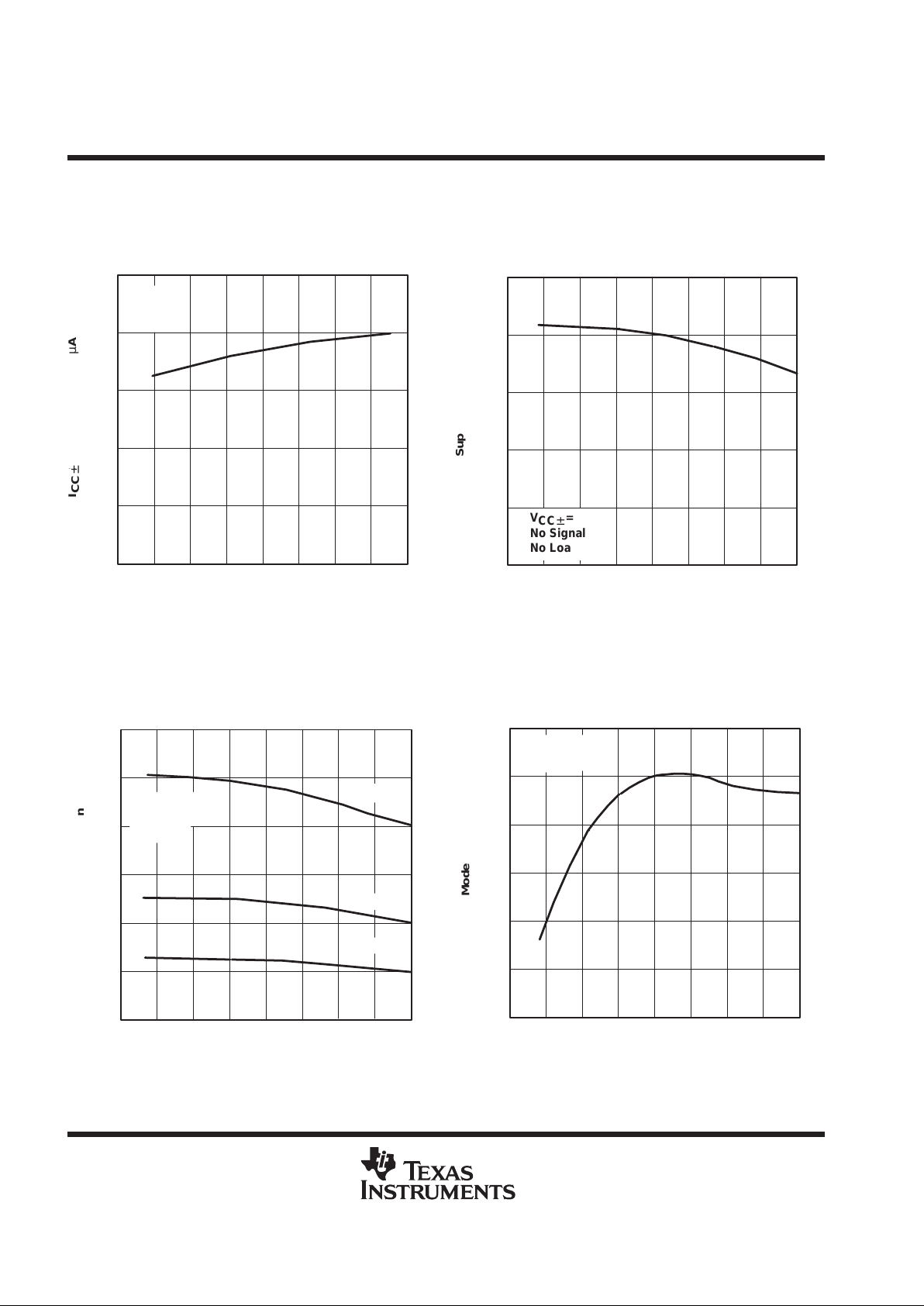
TYPICAL CHARACTERISTICS
Table of Graphs
FIGURE
Maximum peak output voltage vs Supply voltage 4
Maximum peak output voltage vs Free-air temperature 5
Maximum peak output voltage vs Load resistance 6
Maximum peak output voltage vs Frequency 7
Differential voltage amplification vs Free-air temperature 8
Large-signal differential voltage amplification vs Frequency 9
Phase shift vs Frequency 9
Supply current vs Supply voltage 10
Supply current vs Free-air temperature 11
Total power dissipation vs Free-air temperature 12
Common-mode rejection ratio vs Free-air temperature 13
Normalized unity-gain bandwidth vs Free-air temperature 14
Normalized slew rate vs Free-air temperature 14
Normalized phase shift vs Free-air temperature 14
Input bias current vs Free-air temperature 15
Voltage-follower large-signal pulse response vs T ime 16
Output voltage vs Elapsed time 17
Equivalent input noise voltage vs Frequency 18

TL061, TL061A, TL061B, TL061Y, TL062, TL062A
TL062B, TL062Y, TL064, TL064A, TL064B, TL064Y
LOW-POWER JFET-INPUT OPERATIONAL AMPLIFIERS
SLOS078F – NOVEMBER 1978 – REVISED JANUARY 1999
14
POST OFFICE BOX 655303 • DALLAS, TEXAS 75265
TYPICAL CHARACTERISTICS
†
Figure 4
0
0
VOM – Maximum Peak Output Voltage – V
|V
CC±
| – Supply Voltage – V
±2.5
±5
±7.5
±10
±12.5
±15
2 4 6 8 10 12 14 16
RL = 10 kΩ
TA = 25°C
See Figure 2
MAXIMUM PEAK OUTPUT VOLTAGE
vs
SUPPLY VOLTAGE
V
OM
Figure 5
–75
0
VOM – Maximum Peak Output Voltage – V
TA – Free-Air Temperature – °C
±2.5
±5
±7.5
±10
±12.5
±15
–50 –25 0 25 50 75 100 125
V
CC±
= ±15 V
RL = 10 kΩ
See Figure 2
MAXIMUM PEAK OUTPUT VOLTAGE
vs
FREE-AIR TEMPERATURE
V
OM
Figure 6
See Figure 2
TA = 25°C
V
CC±
= ±15 V
0
100
VOM – Maximum Peak Output Voltage – V
RL – Load Resistance – Ω
1 k 10 k
±2.5
±5
±7.5
±10
±12.5
±15
200 400 700 2 k 4 k 7 k
MAXIMUM PEAK OUTPUT VOLTAGE
vs
LOAD RESISTANCE
V
OM
V
CC±
= ±12 V
V
CC±
= ±5 V
f – Frequency – Hz
1 k
0
VOM – Maximum Peak Output Voltage – V
10 k 100 k 1 M
10 M
±2.5
±5
±7.5
±10
±12.5
±15
MAXIMUM PEAK OUTPUT VOLTAGE
vs
FREQUENCY
RL = 10 kΩ
TA = 25°C
See Figure 2
V
OM
V
CC
±
= ±15 V
Figure 7
†
Data at high and low temperatures are applicable only within the specified operating free-air temperature ranges of the various devices.

TL061, TL061A, TL061B, TL061Y, TL062, TL062A
TL062B, TL062Y, TL064, TL064A, TL064B, TL064Y
LOW-POWER JFET-INPUT OPERATIONAL AMPLIFIERS
SLOS078F – NOVEMBER 1978 – REVISED JANUARY 1999
15
POST OFFICE BOX 655303 • DALLAS, TEXAS 75265
TYPICAL CHARACTERISTICS
†
– Differential Voltage Amplification – V/mV
A
VD
RL = 10 kΩ
V
CC±
= ±15 V
1
–75
TA – Free-Air Temperature – °C
–50 –25 0 25 50 75 100 125
2
4
10
7
DIFFERENTIAL VOLTAGE AMPLIFICATION
vs
FREE-AIR TEMPERATURE
Figure 8
A
VD
(left scale)
1
.001
f – Frequency – Hz
10 100 1 k 10 k 100 k 1 M 10 M
.01
.1
1
10
100
Phase Shift
135°
90°
180°
45°
0°
V
CC±
= ±15 V
R
ext
= 0
RL = 10 kΩ
TA = 25°C
Phase Shift
(right scale)
LARGE-SIGNAL
DIFFERENTIAL VOLTAGE
AMPLIFICATION AND PHASE SHIFT
vs
FREQUENCY
– Large-Signal Differential
A
VD
Voltage Amplification – V/mV
Figure 9
†
Data at high and low temperatures are applicable only within the specified operating free-air temperature ranges of the various devices.
TL061, TL061A, TL061B, TL061Y, TL062, TL062A
TL062B, TL062Y, TL064, TL064A, TL064B, TL064Y
LOW-POWER JFET-INPUT OPERATIONAL AMPLIFIERS
SLOS078F – NOVEMBER 1978 – REVISED JANUARY 1999
16
POST OFFICE BOX 655303 • DALLAS, TEXAS 75265
TYPICAL CHARACTERISTICS
†
Figure 10
TA = 25°C
No Signal
No Load
0
0
2 4 6 8 10 12 14 16
50
100
150
200
250
SUPPLY CURRENT
vs
SUPPLY VOLTAGE
|V
CC±
| – Supply Voltage – V
ICC – Supply Current –
I
CC
µA
±
Figure 11
–75
0
ICC – Supply Current –
TA – Free-Air Temperature – °C
50
100
150
200
250
–50 –25 0 25 50 75 100 125
SUPPLY CURRENT
vs
FREE-AIR TEMPERATURE
I
CC
µA
±
V
CC±
= ±15 V
No Signal
No Load
Figure 12
–75
0
TA – Free-Air Temperature – °C
5
10
15
20
25
30
–50 –25 0 25 50 75 100 125
V
CC±
= ±15 V
No Signal
No Load
TL064
TL062
TL061
TOTAL POWER DISSIPATION
vs
FREE-AIR TEMPERATURE
PD – Total Power Dissipation – mW
ÁÁ
P
D
Figure 13
81
CMRR – Common-Mode Rejection Ratio – dB
1251007550250–25–50
TA – Free-Air Temperature – °C
–75
82
83
84
85
86
87
V
CC±
= ±15 V
RL = 10 kΩ
ALL EXCEPT TL06_C
COMMON-MODE REJECTION RATIO
vs
FREE-AIR TEMPERATURE
†
Data at high and low temperatures are applicable only within the specified operating free-air temperature ranges of the various devices.
TL061, TL061A, TL061B, TL061Y, TL062, TL062A
TL062B, TL062Y, TL064, TL064A, TL064B, TL064Y
LOW-POWER JFET-INPUT OPERATIONAL AMPLIFIERS
SLOS078F – NOVEMBER 1978 – REVISED JANUARY 1999
17
POST OFFICE BOX 655303 • DALLAS, TEXAS 75265
TYPICAL CHARACTERISTICS
0.7
Normalized Unity-Gain Bandwidth and Slew Rate
125
1007550250–25–50
TA – Free-Air Temperature – °C
–75
0.8
0.9
1
1.1
1.2
1.3
1.02
1.01
1
0.99
0.98
0.97
Normalized Phase Shift
1.03
V
CC±
= ±15 V
RL = 10 kΩ
f = B1 for Phase Shift
Unity-Gain Bandwidth
(left scale)
Phase Shift
(right scale)
Slew Rate
(left scale)
NORMALIZED UNITY-GAIN BANDWIDTH,
SLEW RATE, AND PHASE SHIFT
vs
FREE-AIR TEMPERATURE
Figure 14
1251007550250–25
0.01
IIB – Input Bias Current – nA
–50
TA – Free-Air Temperature – °C
0.04
0.1
0.4
1
4
10
40
100
INPUT BIAS CURRENT
vs
FREE-AIR TEMPERATURE
V
CC±
= ±15 V
I
IB
Figure 15 Figure 16
–6
Input and Output Voltages – V
t – Time – µs
Input
Output
V
CC±
= ±15 V
RL = 10 kΩ
CL = 100 pF
TA = 25°C
0246810
–4
–2
0
2
4
6
VOLTAGE-FOLLOWER
LARGE-SIGNAL PULSE RESPONSE
vs
TIME

TL061, TL061A, TL061B, TL061Y, TL062, TL062A
TL062B, TL062Y, TL064, TL064A, TL064B, TL064Y
LOW-POWER JFET-INPUT OPERATIONAL AMPLIFIERS
SLOS078F – NOVEMBER 1978 – REVISED JANUARY 1999
18
POST OFFICE BOX 655303 • DALLAS, TEXAS 75265
TYPICAL CHARACTERISTICS
Figure 17
–4
– Output Voltage – mV
t – Elapsed Time – µs
0 0.2 0.4 0.6 0.8 1 1.2 1.4
0
4
8
12
16
20
24
28
V
CC±
= ±15 V
RL = 10 kΩ
TA = 25°C
10%
t
r
Overshoot
90%
OUTPUT VOLTAGE
vs
ELAPSED TIME
V
O
0
Vn – Equivalent Input Noise Voltage –
f – Frequency – Hz
10
20
30
40
50
60
70
80
90
100
10 40 100 400 1 k 4 k 10 k 40 k 100 k
EQUIVALENT INPUT NOISE VOLTAGE
vs
FREQUENCY
V
CC±
= ±15 V
RS = 20 Ω
TA = 25°C
V
n
nV/
Hz
Figure 18
TL061, TL061A, TL061B, TL061Y, TL062, TL062A
TL062B, TL062Y, TL064, TL064A, TL064B, TL064Y
LOW-POWER JFET-INPUT OPERATIONAL AMPLIFIERS
SLOS078F – NOVEMBER 1978 – REVISED JANUARY 1999
19
POST OFFICE BOX 655303 • DALLAS, TEXAS 75265
APPLICATION INFORMATION
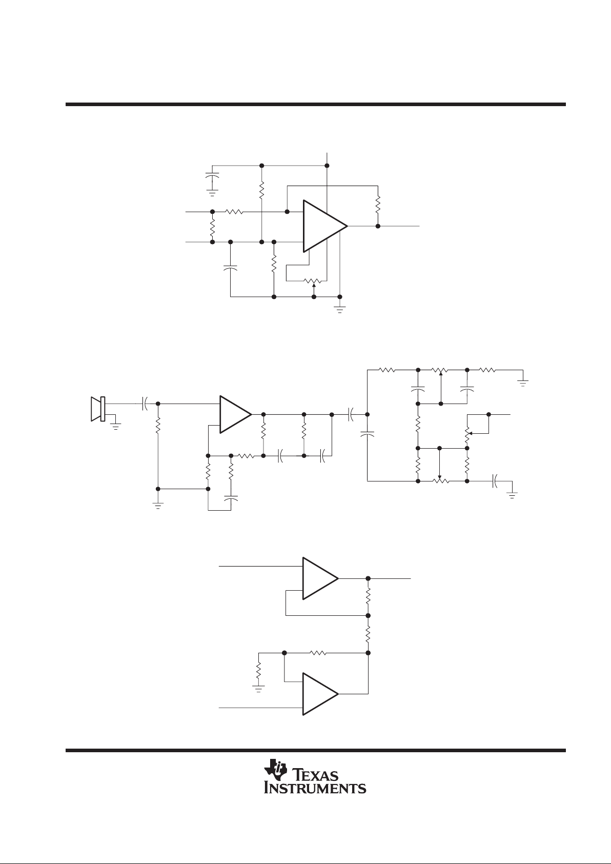
Table of Application Diagrams
APPLICATION DIAGRAM
PART
NUMBER
FIGURE
Instrumentation amplifier TL064 19
0.5-Hz square-wave oscillator TL061 20
High-Q notch filter TL061 21
Audio-distribution amplifier TL064 22
Low-level light detector preamplifier TL061 23
AC amplifier TL061 24
Microphone preamplifier with tone control TL061 25
Instrumentation amplifier TL062 26
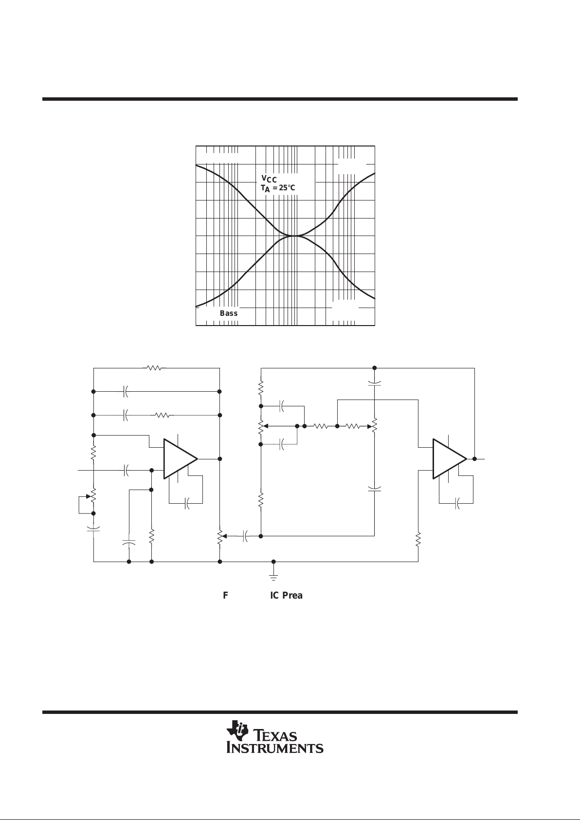
IC preamplifier TL062 27
+
–
–
+
+
–
+
–
TL064
V
CC+
V
CC–
100 kΩ
Input B
10 kΩ
0.1% 0.1%
10 kΩ
V
CC–
V
CC+
TL064
Input A
V
CC+
TL064
V
CC–
100 kΩ
10 kΩ
0.1%
10 kΩ
0.1%
TL064
V
CC–
V
CC+
100 kΩ
100 kΩ
Output
1 MΩ
Figure 19. Instrumentation Amplifier
TL061
+
–
–15 V
15 V
Output
1 kΩ
9.1 kΩ
3.3 kΩ
CF = 3.3 µF
RF = 100 kΩ
3.3 kΩ
f
+
1
2p
R
F
C
F
Figure 20. 0.5-Hz Square-Wave Oscillator
TL061
+
–
R2
R1
C1 C2
R3
C3
V
CC–
V
CC+
OutputInput
C1+C2
+
C3
2
+
110 pF
f
o
+
1
2p R1
C1
+
1kHz
R1 = R2 = 2
× R3 = 1.5 MΩ
Figure 21. High-Q Notch Filter
TL061, TL061A, TL061B, TL061Y, TL062, TL062A
TL062B, TL062Y, TL064, TL064A, TL064B, TL064Y
LOW-POWER JFET-INPUT OPERATIONAL AMPLIFIERS
SLOS078F – NOVEMBER 1978 – REVISED JANUARY 1999
20
POST OFFICE BOX 655303 • DALLAS, TEXAS 75265
APPLICATION INFORMATION
+
–
+
–
TL064
Output C
V
CC+
V
CC+
Output B
TL064
–
+
V
CC+
Output A
TL064
–
+
V
CC+
TL064
V
CC+
100 kΩ
100 µF
Input
1 µF
1 MΩ
100 kΩ
100 kΩ
Figure 22. Audio-Distribution Amplifier
+
–
TIL601
10 kΩ
15 V
Output
–15 V
5 kΩ
100 pF
TL061
10 kΩ
10 kΩ
10 kΩ
10 kΩ
10 kΩ
Figure 23. Low-Level Light Detector Preamplifier
TL061, TL061A, TL061B, TL061Y, TL062, TL062A
TL062B, TL062Y, TL064, TL064A, TL064B, TL064Y
LOW-POWER JFET-INPUT OPERATIONAL AMPLIFIERS
SLOS078F – NOVEMBER 1978 – REVISED JANUARY 1999
21
POST OFFICE BOX 655303 • DALLAS, TEXAS 75265
APPLICATION INFORMATION
TL061
N2
+
–
0.1 µF
10 kΩ
50 Ω
250 kΩ
N1
Output
1 MΩ
V
CC+
10 kΩ
10 kΩ
0.1 µF
Figure 24. AC Amplifier
1.2 MΩ 100 kΩ
20 µF
+
–
0.1 µF
47 kΩ
TL061
2.7 kΩ
270 Ω
0.003 µF 0.001 µF
0.002 µF
1 µF
10 kΩ
100 kΩ
50 kΩ
0.06 µF
50 kΩ
10 kΩ 100 kΩ 1 kΩ
0.06 µF
10 kΩ
0.02 µF
100 kΩ
+
Figure 25. Microphone Preamplifier With Tone Control
IN–
IN+
100 kΩ
TL062
TL062
1 kΩ
1 kΩ
100 kΩ
–
+
–
+
Output
Figure 26. Instrumentation Amplifier
TL061, TL061A, TL061B, TL061Y, TL062, TL062A
TL062B, TL062Y, TL064, TL064A, TL064B, TL064Y
LOW-POWER JFET-INPUT OPERATIONAL AMPLIFIERS
SLOS078F – NOVEMBER 1978 – REVISED JANUARY 1999
22
POST OFFICE BOX 655303 • DALLAS, TEXAS 75265
APPLICATION INFORMATION
TL062
220 kΩ
–
+
0.00375 µF
TL062
–
+
10 pF
68 kΩ
0.003 µF
0.03 µF
0.03 µF
10 kΩ 3.3 kΩ
0.003 µF
V
CC–
V
CC+
Output
Input
V
CC–
V
CC+
10 pF
MIN
MAX
100 kΩ
Treble
MIN
MAX
100 kΩ
Bass
10 kΩ
10 kΩ
+
0.01 µF
27 kΩ
100 Ω
Balance
100 Ω
50 pF
+
75 µF
47 µF
5 kΩ
Gain
47 kΩ
1 µF
TA = 25°C
V
CC±
= ±15 V
Max
Treble
Max Bass
200 10 k4 k2 k1 k40040 100
20
15
10
5
0
–5
–10
–15
–20
–25
20 k
25
f – Frequency – Hz
Voltage Amplification – dB
20
IC PREAMPLIFIER RESPONSE CHARACTERISTICS
Min
Treble
Min Bass
Figure 27. IC Preamplifier

IMPORTANT NOTICE
T exas Instruments and its subsidiaries (TI) reserve the right to make changes to their products or to discontinue
any product or service without notice, and advise customers to obtain the latest version of relevant information
to verify, before placing orders, that information being relied on is current and complete. All products are sold
subject to the terms and conditions of sale supplied at the time of order acknowledgement, including those
pertaining to warranty, patent infringement, and limitation of liability.
TI warrants performance of its semiconductor products to the specifications applicable at the time of sale in
accordance with TI’s standard warranty. Testing and other quality control techniques are utilized to the extent
TI deems necessary to support this warranty. Specific testing of all parameters of each device is not necessarily
performed, except those mandated by government requirements.
CERT AIN APPLICATIONS USING SEMICONDUCTOR PRODUCTS MA Y INVOLVE POTENTIAL RISKS OF
DEATH, PERSONAL INJURY, OR SEVERE PROPERTY OR ENVIRONMENTAL DAMAGE (“CRITICAL
APPLICATIONS”). TI SEMICONDUCTOR PRODUCTS ARE NOT DESIGNED, AUTHORIZED, OR
WARRANTED TO BE SUITABLE FOR USE IN LIFE-SUPPORT DEVICES OR SYSTEMS OR OTHER
CRITICAL APPLICATIONS. INCLUSION OF TI PRODUCTS IN SUCH APPLICA TIONS IS UNDERST OOD TO
BE FULLY AT THE CUSTOMER’S RISK.
In order to minimize risks associated with the customer’s applications, adequate design and operating
safeguards must be provided by the customer to minimize inherent or procedural hazards.
TI assumes no liability for applications assistance or customer product design. TI does not warrant or represent
that any license, either express or implied, is granted under any patent right, copyright, mask work right, or other
intellectual property right of TI covering or relating to any combination, machine, or process in which such
semiconductor products or services might be or are used. TI’s publication of information regarding any third
party’s products or services does not constitute TI’s approval, warranty or endorsement thereof.
Copyright 1998, Texas Instruments Incorporated
 Loading...