www.DataSheet4U.com
D
Direct Upgrades to TL07x and TL08x BiFET
Operational Amplifiers
D
Faster Slew Rate (20 V/µs Typ) Without
Increased Power Consumption
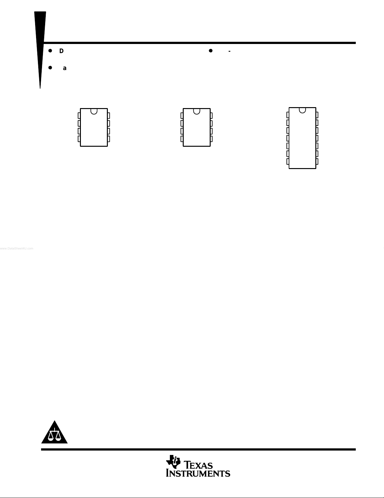
TL051
D OR P PACKAGE
(TOP VIEW)
D
TL052
D, P, OR PS PACKAGE
(TOP VIEW)
TL05x, TL05xA
ENHANCED-JFET LOW-OFFSET
OPERATIONAL AMPLIFIERS
SLOS178A – FEBRUARY 1997 - REVISED FEBRUARY 2003
On-Chip Offset-Voltage Trimming for
Improved DC Performance and Precision
Grades Are Available (1.5 mV, TL051A)
D, DB, N, OR NS PACKAGE
TL054
(TOP VIEW)
OFFSET N1
IN–
IN+
V
CC–
1
2
3
4
NC
8
V
7
CC+
OUT
6
OFFSET N2
5
1OUT
1IN–
1IN+
V
CC–
1
2
3
4
8
7
6
5
V
CC+
2OUT
2IN–
2IN+
1OUT
1IN–
1IN+
V
CC+
2IN+
2IN–
2OUT
1
2
3
4
5
6
7
14
13
12
11
10
9
8
4OUT
4IN–
4IN+
V
3IN+
3IN–
3OUT
description/ordering information
The TL05x series of JFET-input operational amplifiers of fers improved dc and ac characteristics over the TL07x
and TL08x families of BiFET operational amplifiers. On-chip Zener trimming of offset voltage yields precision
grades as low as 1.5 mV (TL051A) for greater accuracy in dc-coupled applications. T exas Instruments improved
BiFET process and optimized designs also yield improved bandwidth and slew rate without increased power
consumption. The TL05x devices are pin-compatible with the TL07x and TL08x and can be used to upgrade
existing circuits or for optimal performance in new designs.
BiFET operational amplifiers offer the inherently higher input impedance of the JFET -input transistors, without
sacrificing the output drive associated with bipolar amplifiers. This makes them better suited for interfacing with
high-impedance sensors or very low-level ac signals. They also feature inherently better ac response than
bipolar or CMOS devices having comparable power consumption.
The TL05x family was designed to offer higher precision and better ac response than the TL08x, with the low
noise floor of the TL07x. Designers requiring significantly faster ac response or ensured lower noise should
consider the Excalibur TLE208x and TLE207x families of BiFET operational amplifiers.
CC–
Because BiFET operational amplifiers are designed for use with dual power supplies, care must be taken to
observe common-mode input voltage limits and output swing when operating from a single supply . DC biasing
of the input signal is required, and loads should be terminated to a virtual-ground node at mid-supply. Texas
Instruments TLE2426 integrated virtual ground generator is useful when operating BiFET amplifiers from single
supplies.
The TL05x are fully specified at ±15 V and ±5 V. For operation in low-voltage and/or single-supply systems,
Texas Instruments LinCMOS families of operational amplifiers (TLC-prefix) are recommended. When moving
from BiFET to CMOS amplifiers, particular attention should be paid to the slew rate and bandwidth
requirements, and also the output loading.
Please be aware that an important notice concerning availability, standard warranty, and use in critical applications of
Texas Instruments semiconductor products and disclaimers thereto appears at the end of this data sheet.
PRODUCTION DATA information is current as of publication date.
Products conform to specifications per the terms of Texas Instruments
standard warranty. Production processing does not necessarily include
testing of all parameters.
POST OFFICE BOX 655303 • DALLAS, TEXAS 75265
Copyright 2003, Texas Instruments Incorporated
1
TL05x, TL05xA
PDIP (P)
Tube of 50
052AC
PDIP (P)
Tube of 50
TL051C
0°C to 70°C
SOIC (D)
TL052C
TL054C
4 mV
SOIC (D)
TL054C
SOIC (D)
052AI
PDIP (P)
Tube of 50
40°C to 85°C
1.5 mV
TL052I
TL054AI
SOIC (D)
TL054I
ENHANCED-JFET LOW-OFFSET
OPERATIONAL AMPLIFIERS
SLOS178A – FEBRUARY 1997 - REVISED FEBRUARY 2003
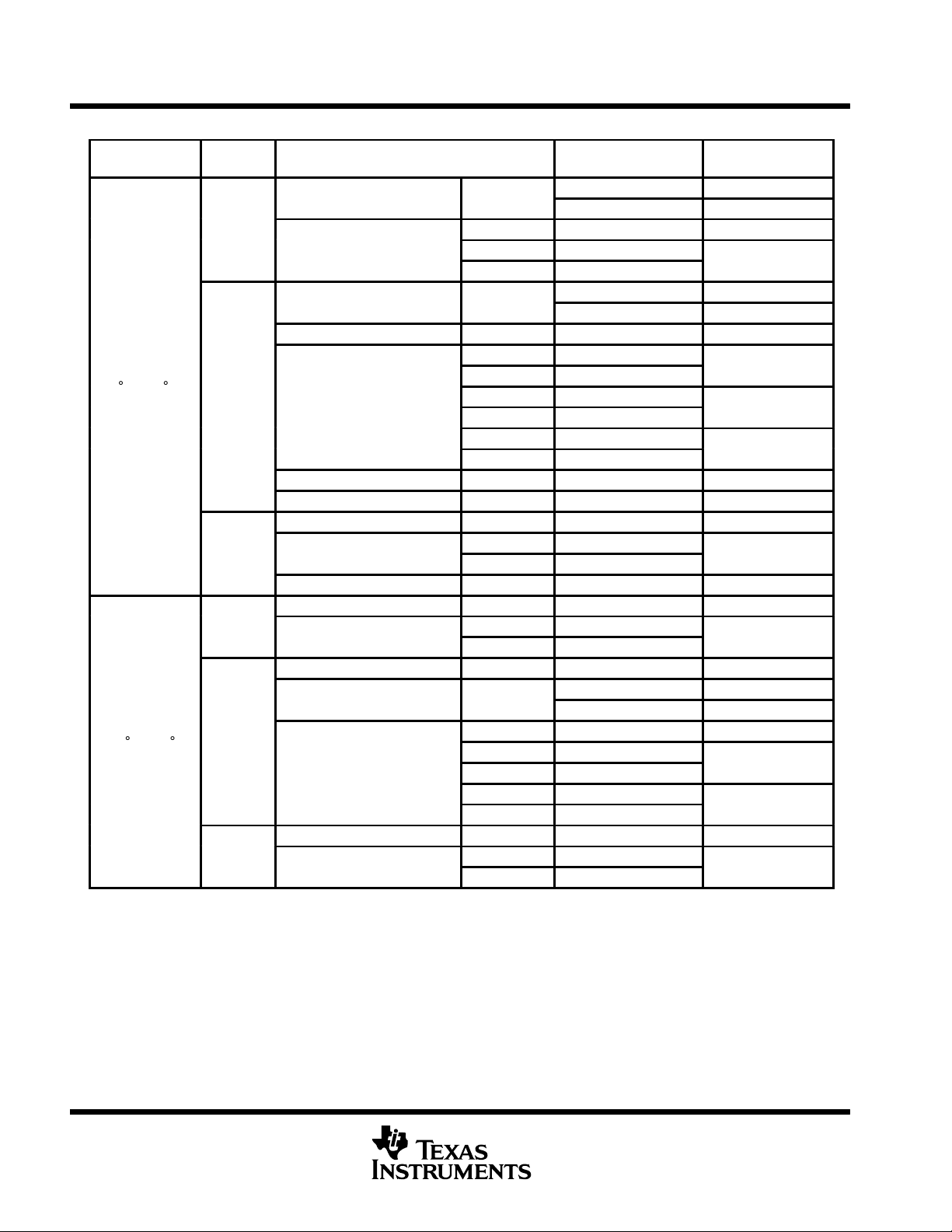
ORDERING INFORMATION
T
A
–
†
Package drawings, standard packing quantities, thermal data, symbolization, and PCB design guidelines are available at
www.ti.com/sc/package.
VIOmax
AT 25°C
800 µV
1.5 mV
800 µV
4 mV
PACKAGE
SOIC (D)
PDIP (N) Tube of 25 TL054ACN TL054ACN
SOP (PS) Reel of 2000 TL052CPSR TL052
SSOP (DB) Reel of 2000 TL054CDBR TL054
PDIP (N) Tube of 25 TL054CN TL054CN
SOP (NS) Reel of 2000 TL054CNSR TL054
PDIP (P) Tube of 50 TL052AIP TL052AI
PDIP (N) Tube of 25 TL054AIN TL054AIN
SOIC (D)
PDIP (N) Tube of 25 TL054IN TL054IN
†
Tube of 75 TL051ACD 051AC
Tube of 75 TL052ACD
Reel of 2500 TL052ACDR
Tube of 75 TL051CD
Reel of 2500 TL051CDR
Tube of 75 TL052CD
Reel of 2500 TL052CDR
Tube of 50 TL054ACD
Reel of 2500 TL054ACDR
Tube of 50 TL054CD
Reel of 2500 TL054CDR
Tube of 75 TL052AID
Reel of 2500 TL052AIDR
Tube of 75 TL051ID TL051I
Tube of 75 TL052ID
Reel of 2500 TL052IDR
Tube of 50 TL054AID
Reel of 2500 TL054AIDR
Tube of 50 TL054ID
Reel of 2500 TL054IDR
ORDERABLE
PART NUMBER
TL051ACP TL051ACP
TL052ACP TL052ACP
TL051CP TL051CP
TL052CP TL052CP
TL051IP TL051IP
TL052IP TL052IP
TOP-SIDE
MARKING
2
POST OFFICE BOX 655303 • DALLAS, TEXAS 75265
T
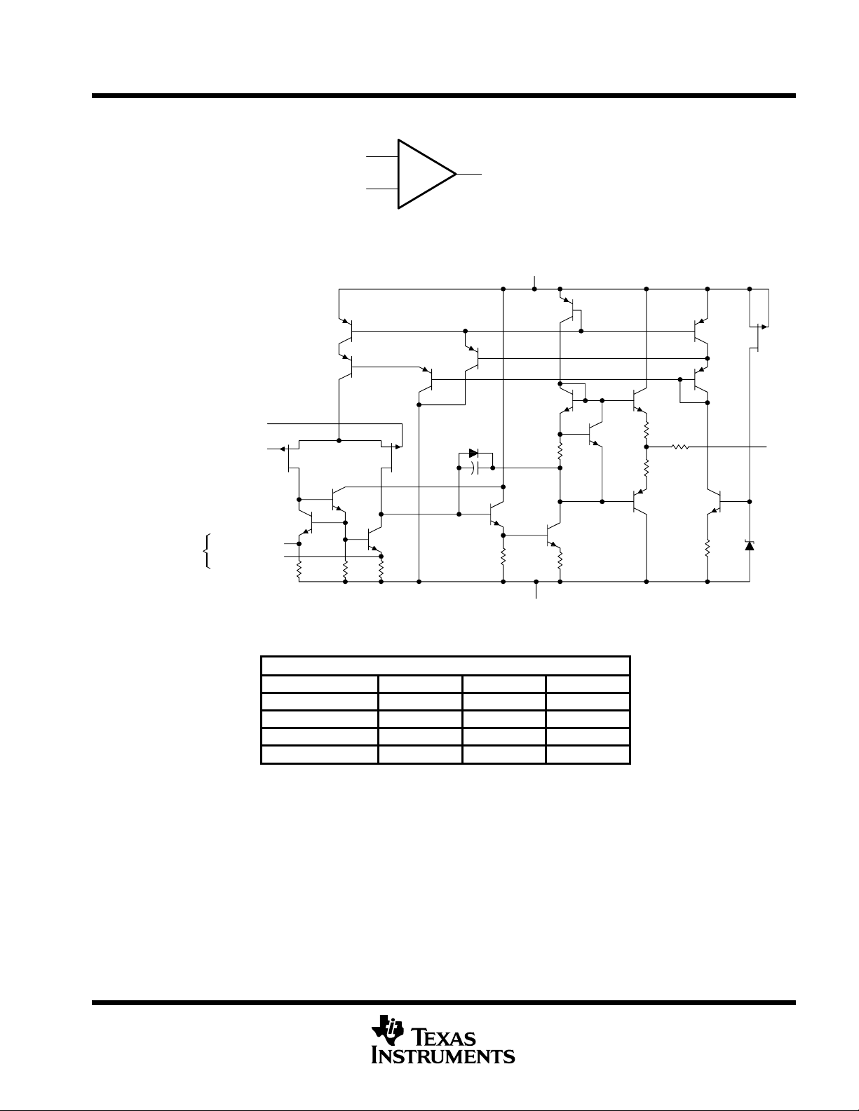
symbol (each amplifier)
TL05x, TL05xA
ENHANCED-JFET LOW-OFFSET
OPERATIONAL AMPLIFIERS
SLOS178A – FEBRUARY 1997 - REVISED FEBRUARY 2003
IN–
IN+
equivalent schematic (each amplifier)
Q2
Q3
IN+
IN–
JF1 JF2
Q4
Q1
See Note A
OFFSET N1
OFFSET N2
R1
R2 R3
Q5
–
+
Q6
Q7
D1
C1
R4
OUT
Q8
V
CC+
R5
R6
Q10
Q11
Q9
Q12
R8
Q13
R7
R9
Q14
R10 D2
Q17
Q15
Q16
JF3
OU
NOTE A: OFFSET N1 and OFFSET N2 are available only on the TL051x.
ACTUAL DEVICE COMPONENT COUNT
COMPONENT TL051 TL052 TL054
Transistors 20 34 62
Resistors 10 19 37
Diodes 2 3 5
Capacitors 1 2 4
†
These figures include all four amplifiers and all ESD, bias, and trim circuitry.
V
CC–
†
POST OFFICE BOX 655303 • DALLAS, TEXAS 75265
3
TL05x, TL05xA
UNIT
VICCommon-mode input voltage
V
ENHANCED-JFET LOW-OFFSET
OPERATIONAL AMPLIFIERS
SLOS178A – FEBRUARY 1997 - REVISED FEBRUARY 2003
absolute maximum ratings over operating free-air temperature range (unless otherwise noted)
Supply voltage, V
Supply voltage, V
Differential input voltage (see Note 2) ±30 V. . . . . . . . . . . . . . . . . . . . . . . . . . . . . . . . . . . . . . . . . . . . . . . . . . . . . . . .
Input voltage range, V
Input current, I
I
Output current, I
Total current into V
Total current out of V
Duration of short-circuit current at (or below) 25°C Unlimited. . . . . . . . . . . . . . . . . . . . . . . . . . . . . . . . . . . . . . . . .
Package thermal impedance, θ
Operating virtual junction temperature, T
Lead temperature 1,6 mm (1/16inch) from case for 10 seconds 260°C. . . . . . . . . . . . . . . . . . . . . . . . . . . . . . . .
Storage temperature range –65°C to 150°C. . . . . . . . . . . . . . . . . . . . . . . . . . . . . . . . . . . . . . . . . . . . . . . . . . . . . . . .
†
Stresses beyond those listed under “absolute maximum ratings” may cause permanent damage to the device. These are stress ratings only, and
functional operation of the device at these or any other conditions beyond those indicated under “recommended operating conditions” is not
implied. Exposure to absolute-maximum-rated conditions for extended periods may affect device reliability.
NOTES: 1. All voltage values, except differential voltages, are with respect to the midpoint between V
2. Differential voltages are at IN+ with respect to IN–.
3. The magnitude of the input voltage must never exceed the magnitude of the supply voltage or 15 V, whichever is less.
4. Maximum power dissipation is a function of TJ(max),
ambient temperature is PD = (TJ(max) – TA)/
5. The package thermal impedance is calculated in accordance with JESD 51-7.
(see Note 1) 18 V. . . . . . . . . . . . . . . . . . . . . . . . . . . . . . . . . . . . . . . . . . . . . . . . . . . . . . . . . . .
CC+
(see Note 1) –18 V. . . . . . . . . . . . . . . . . . . . . . . . . . . . . . . . . . . . . . . . . . . . . . . . . . . . . . . . . .
CC–
(any input, see Notes 1 and 3) ±15 V. . . . . . . . . . . . . . . . . . . . . . . . . . . . . . . . . . . . . . . . .
I
(each input) ±1 mA. . . . . . . . . . . . . . . . . . . . . . . . . . . . . . . . . . . . . . . . . . . . . . . . . . . . . . . . . . . . . . .
(each output) ±80 mA. . . . . . . . . . . . . . . . . . . . . . . . . . . . . . . . . . . . . . . . . . . . . . . . . . . . . . . . . .
O
160 mA. . . . . . . . . . . . . . . . . . . . . . . . . . . . . . . . . . . . . . . . . . . . . . . . . . . . . . . . . . . . . . . . . .
CC+
160 mA. . . . . . . . . . . . . . . . . . . . . . . . . . . . . . . . . . . . . . . . . . . . . . . . . . . . . . . . . . . . . . . . .
CC–
(see Notes 4 and 5): D package (8 pin) 97°C/W. . . . . . . . . . . . . . . . . . . . . .
JA
D package (14 pin) 86°C/W. . . . . . . . . . . . . . . . . . . . .
DB package (14 pin) 96°C/W. . . . . . . . . . . . . . . . . . .
N package (14 pin) 80°C/W. . . . . . . . . . . . . . . . . . . . .
NS package (14 pin) 76°C/W. . . . . . . . . . . . . . . . . . .
P package (8 pin) 85°C/W. . . . . . . . . . . . . . . . . . . . . .
PS package (8 pin) 95°C/W. . . . . . . . . . . . . . . . . . . .
150°C. . . . . . . . . . . . . . . . . . . . . . . . . . . . . . . . . . . . . . . . . . . . . . . . . . .
J
and V
CC+
θ
, and TA. The maximum allowable power dissipation at any allowable
θ
JA
JA
. Operating at the absolute maximum TJ of 150°C can impact reliability.
CC–.
†
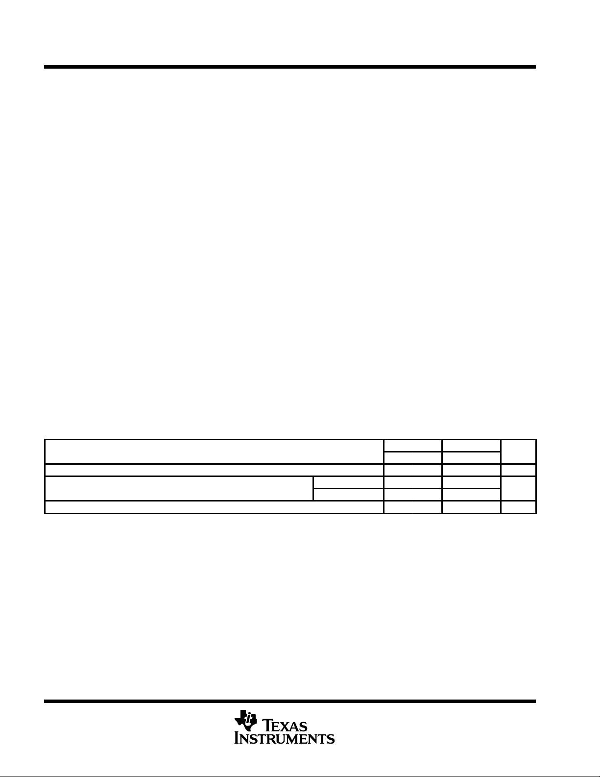
recommended operating conditions
V
T
CC±
A
Supply voltage ±5 ±15 ±5 ±15 V
p
Operating free-air temperature 0 70 –40 85 °C
C SUFFIX I SUFFIX
MIN MAX MIN MAX
V
= ±5 V –1 4 –1 4
CC±
V
= ±15 V –11 11 –11 11
CC±
4
POST OFFICE BOX 655303 • DALLAS, TEXAS 75265
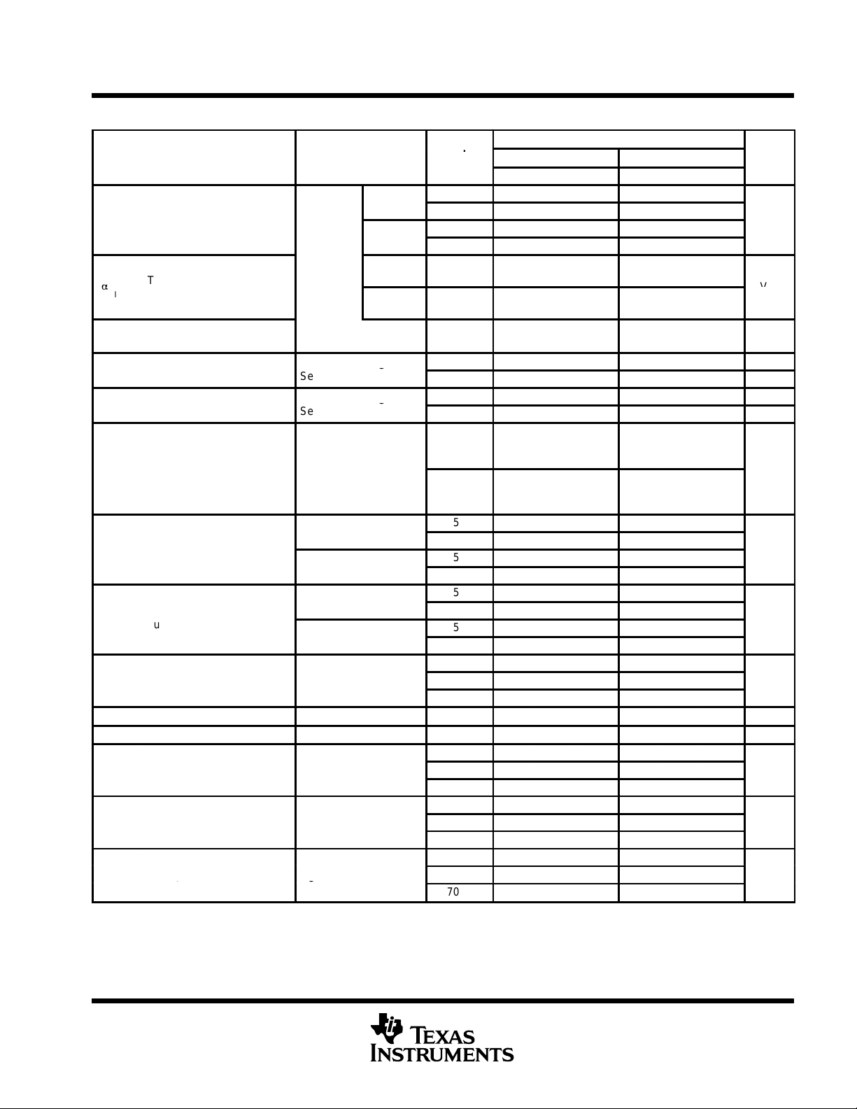
†
TL051C
VIOInput offset voltage
mV
TL051AC
V
0
a
R
S
Ω
V/°C
IIOInput offset current
OIC
IIBInput bias current
OIC
V
V
R
10 kΩ
V
V
R
2 kΩ
R
10 kΩ
V
g
V
R
2 kΩ
L
diff
l
¶
voltage am lification
¶
C
V
V
i
rejection ratio
V
O
R
S
Ω
S
ratio (∆V
CC±
/∆VIO)
CCyO
TL05x, TL05xA
ENHANCED-JFET LOW-OFFSET
OPERATIONAL AMPLIFIERS
SLOS178A – FEBRUARY 1997 - REVISED FEBRUARY 2003
TL051C and TL051AC electrical characteristics at specified free-air temperature
TL051C, TL051AC
PARAMETER TEST CONDITIONS
p
,
=
O
Temperature coefficient
V
IO
of input offset voltage
Input offset-voltage
long-term drift
p
p
ICR
OM+
OM–
A
VD
r
i
c
i
CMRR
k
SVR
I
CC
†
Full range is 0°C to 70°C.
‡
This parameter is tested on a sample basis for the TL051A. For other test requirements, please contact the factory. This statement has no bearing
on testing or nontesting of other parameters.
§
Typical values are based on the input offset-voltage shift observed through 168 hours of operating life test at TA = 150°C, extrapolated to
TA = 25°C using the Arrhenius equation, and assuming an activation energy of 0.96 eV .
¶
For V
Common-mode input
voltage range
Maximum positive peak
output voltage swing
Maximum negative peak
output voltage swing
arge-signal
Input resistance 25°C 10
Input capacitance 25°C 10 12 pF
ommon-mode
upply-voltage rejection
Supply current VO = 0, No load
= ±5 V, VO = ±2.3 V, or for V
CC±
p
‡
§
erentia
VIC = 0,
R
= 50 Ω
= 50
VO = 0, VIC = 0,
See Figure 5
VO = 0, VIC = 0,
See Figure 5
=
L
=
L
=
L
=
L
RL = 2 kΩ
=
IC
= 0,
VO = 0, RS = 50 Ω
= ±15 V, VO = ±10 V.
CC±
ICR
TL051C
TL051AC
n,
m
= 50
T
A
25°C 0.75 3.5 0.59 1.5
Full range 4.5 2.5
25°C 0.55 2.8 0.35 0.8
Full range 3.8 1.8
25°C to
70°C
25°C to
70°C
25°C 0.04 0.04 µV/mo
25°C 4 100 5 100 pA
70°C 0.02 1 0.025 1 nA
25°C 20 200 30 200 pA
70°C 0.15 4 0.2 4 nA
25°C
Full range
25°C 3 4.2 13 13.9
Full range 3 13
25°C 2.5 3.8 11.5 12.7
Full range 2.5 11.5
25°C –2.5 –3.5 –12 –13.2
Full range –2.5 –12
25°C –2.3 –3.2 –11 –12
Full range –2.3 –11
25°C 25 59 50 105
0°C 30 65 60 129
70°C 20 46 30 85
25°C 65 85 75 93
0°C 65 84 75 92
70°C 65 84 75 91
25°C 75 99 75 99
0°C 75 98 75 98
70°C 75 97 75 97
25°C 2.6 3.2 2.7 3.2
0°C 2.7 3.2 2.8 3.2
70°C 2.6 3.2 2.7 3.2
V
= ±5 V V
CC±
MIN TYP MAX MIN TYP MAX
8 8
8 8 25
–1
–2.3
to
to
4
5.6
–1
to
4
12
–11
–11
to
11
to
11
CC±
= ±15 V
–12.3
to
15.6
12
10
UNIT
µ
V/mV
Ω
dB
dB
mA
°
POST OFFICE BOX 655303 • DALLAS, TEXAS 75265
5
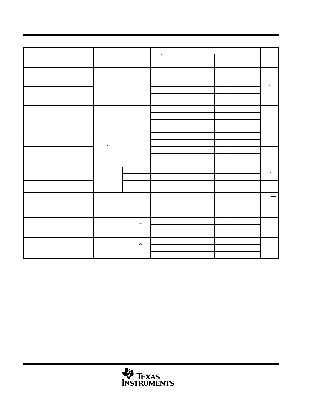
TL05x, TL05xA
†
Positi
L
,
L
,
V/µs
N
ns
C
L
100 F
g
V
q
V/√H
C
L
See Figure 4
Ph
V
10 mV,R
2 kΩ
gain
C
L
See Figure 4
ENHANCED-JFET LOW-OFFSET
OPERATIONAL AMPLIFIERS
SLOS178A – FEBRUARY 1997 - REVISED FEBRUARY 2003
TL051C and TL051AC operating characteristics at specified free-air temperature
TL051C, TL051AC
PARAMETER TEST CONDITIONS
SR+
SR–
t
r
t
f
n
V
N(PP)
I
n
THD
B
1
φ
m
†
Full range is 0°C to 70°C.
‡
For V
CC±
§
This parameter is tested on a sample basis for the TL051A. For other test requirements, please contact the factory. This statement has no bearing
on testing or nontesting of other parameters.
¶
For V
CC±
ve slew rate
§
‡
‡
= ±1 V; for V
I(PP)
O(RMS)
= 1 V; for V
at unity gain
egative slew rate
at unity gain
Rise time
Fall time
Overshoot factor
Equivalent input noise
voltage
Peak-to-peak equivalent
input noise voltage
Equivalent input
noise current
Total harmonic distortion
Unity-gain bandwidth
ase margin at unity
= ±5 V, V
= ±5 V, V
R
= 2 kΩ,C
See Figure 1
V
= ±10 mV ,
I(PP)
RL = 2 kΩ,
See Figures 1 and 2
RS = 20 Ω,
See Figure 3
f = 1 kHz 25°C 0.01 0.01
RS = 1 kΩ,
¶
f = 1 kHz
VI = 10 mV, RL = 2 kΩ,
I
CC±
=
= 25 F,
=
= 25 F,
=
= ±15 V, V
= ±15 V, V
CC±
p
p
p
= 100 pF,
,
f = 10 Hz 25°C 75 75
f = 1 kHz 25°C 18 18 30
f = 10 Hz to
10 kHz
RL = 2 kΩ,
=
L
= ±5 V.
I(PP)
= 6 V.
O(RMS)
T
A
25°C 16 13 20
Full
range
25°C 15 13 18
Full
range
25°C 55 56
0°C 54 55
70°C 63 63
25°C 55 57
0°C 54 56
70°C 62 64
25°C 24 19
0°C 24 19
70°C 24 19
25°C 4 4 µV
25°C 0.003 0.003 %
25°C 3 3.1
0°C 3.2 3.3
70°C 2.7 2.8
25°C 59 62
,
0°C 58 62
70°C 59 62
V
= ±5 V V
CC±
MIN TYP MAX MIN TYP MAX
16.4 11 22.6
16 11 19.3
CC±
= ±15 V
UNIT
%
n
pA/√Hz
MHz
deg
z
6
POST OFFICE BOX 655303 • DALLAS, TEXAS 75265
†
A
TL051I
VIOInput offset voltage
mV
TL051AI
V
0
a
R
S
Ω
V/°C
IIOInput offset current
OIC
IIBInput bias current
OIC
V
V
R
10 kΩ
V
V
R
2 kΩ
R
10 kΩ
V
g
V
R
2 kΩ
L
diff
l
¶
voltage am lification
¶
,
C
V
IC
V
ICR
min,
rejection ratio
S
V
0
ratio (∆V
CC±
/∆VIO)
R
S
Ω
TL05x, TL05xA
ENHANCED-JFET LOW-OFFSET
OPERATIONAL AMPLIFIERS
SLOS178A – FEBRUARY 1997 - REVISED FEBRUARY 2003
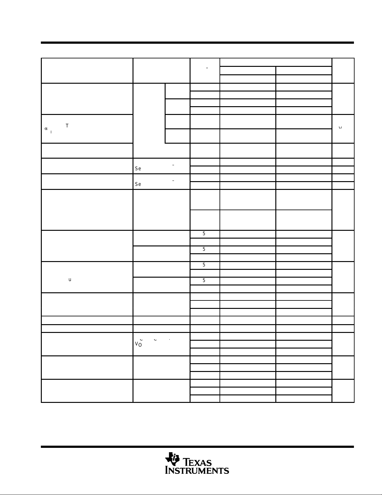
TL051I and TL051AI electrical characteristics at specified free-air temperature
TL051I, TL051AI
PARAMETER TEST CONDITIONS
p
,
=
O
Temperature coefficient of
V
IO
input offset voltage
Input offset-voltage
long-term drift
p
p
ICR
OM +
OM –
A
VD
r
i
c
i
CMRR
k
SVR
I
CC
†
Full range is –40°C to 85°C
‡
This parameter is tested on a sample basis for the TL051A. For other test requirements, please contact the factory. This statement has no bearing
on testing or nontesting of other parameters.
§
Typical values are based on the input offset-voltage shift observed through 168 hours of operating life test at TA = 150°C, extrapolated to
TA = 25°C using the Arrhenius equation, and assuming an activation energy of 0.96 eV .
¶
For V
Common-mode input
voltage range
Maximum positive peak
output voltage swing
Maximum negative peak
output voltage swing
arge-signal
Input resistance 25°C
Input capacitance 25°C 10 12 pF
ommon-mode
upply-voltage rejection
Supply current VO = 0, No load –40°C 2.4 3.2 2.6 3.2 mA
= ±5 V, VO = ±2.3 V, or for V
CC±
‡
§
erentia
p
VIC = 0,
R
= 50 Ω
= 50
VO = 0, VIC = 0,
See Figure 5
VO = 0, VIC = 0,
See Figure 5
=
L
=
L
=
L
=
L
RL = 2 kΩ –40°C 30 74 60 145 V/mV
V
= V
VO = 0,
RS = 50 Ω
=
O
= 50
= ±15 V, VO = ±10 V.
CC±
TL051I
TL051AI
min
,
T
A
25°C 0.75 3.5 0.59 1.5
Full range 5.3 3.3
25°C 0.55 2.8 0.35 0.8
Full range 4.6 2.6
25°C to
85°C
25°C to
85°C
25°C 0.04 0.04 µV/mo
25°C 4 100 5 100 pA
85°C 0.06 10 0.07 10 nA
25°C 20 200 30 200 pA
85°C 0.6 20 0.7 20 nA
25°C
Full range
25°C 3 4.2 13 13.9
Full range 3 13
25°C 2.5 3.8 11.5 12.7
Full range 2.5 11.5
25°C –2.5 –3.5 –12 –13.2
Full range –2.5 –12
25°C –2.3 –3.2 –11 –12
Full range –2.3 –11
25°C 25 59 50 105
85°C 20 43 30 76
25°C 65 85 75 93
–40°C 65 83 75 90 dB
85°C 65 84 75 93
25°C 75 99 75 99
–40°C 75 98 75 98 dB
85°C 75 99 75 99
25°C 2.6 3.2 2.7 3.2
85°C 2.5 3.2 2.6 3.2
V
= ±5 V V
CC±
MIN TYP MAX MIN TYP MAX
7 8
8 8 25
–1
–2.3
to
to
4
5.6
–1
to
4
12
10
–11
–11
to
11
to
11
CC±
= ±15 V
–12.3
to
15.6
12
10
UNIT
µ
Ω
°
POST OFFICE BOX 655303 • DALLAS, TEXAS 75265
7

TL05x, TL05xA
†
Positi
L
,
L
,
V/µs
N
ns
()
C
L
100 F
g
g
V
q
V/√H
C
L
See Figure 4
Ph
V
10 mV,R
2 kΩ
gain
C
L
See Figure 4
ENHANCED-JFET LOW-OFFSET
OPERATIONAL AMPLIFIERS
SLOS178A – FEBRUARY 1997 - REVISED FEBRUARY 2003
TL051I and TL051AI operating characteristics at specified free-air temperature
TL051I, TL051AI
PARAMETER TEST CONDITIONS
SR+
SR–
t
r
t
f
n
V
N(PP)
I
n
THD Total harmonic distortion
B
1
φ
m
†
Full range is –40°C to 85°C.
‡
For V
CC±
§
This parameter is tested on a sample basis for the TL051A. For other test requirements, please contact the factory. This statement has no bearing
on testing or nontesting of other parameters.
¶
For V
CC±
ve slew rate
§
‡
‡
= ±1 V; for V
I(PP)
O(RMS)
= 1 V; for V
at unity gain
egative slew rate
at unity gain
Rise time
Fall time
Overshoot factor
Equivalent input noise
voltage
Peak-to-peak equivalent
input noise voltage
Equivalent input
noise current
Unity-gain bandwidth
ase margin at unity
= ±5 V, V
= ±5 V, V
R
= 2 kΩ,C
See Figure 1
V
= ±10 mV ,
I(PP)
RL = 2 kΩ,
See Fi
RS = 20 Ω,
See Figure 3
f = 1 kHz 25°C 0.01 0.01 pA/√Hz
RS = 1 kΩ,
¶
f = 1 kHz
VI = 10 mV, RL = 2 kΩ,
I
CC±
=
= 25 F,
=
= 25 F,
=
= ±15 V, V
= ±15 V, V
CC±
p
ures 1 and 2
p
p
= 100 pF,
,
f = 10 Hz 25°C 75 75
f = 1 kHz 25°C 18 18 30
f = 10 Hz to
10 kHz
RL = 2 kΩ,
=
L
= ±5 V.
I(PP)
= 6 V.
O(RMS)
T
A
25°C 16 13 20
Full
range
25°C 15 13 18
Full
range
25°C 55 56
–40°C 52 53
85°C 64 65
25°C 55 57
–40°C 51 53
85°C 64 65
25°C 24 19
–40°C 24 19
85°C 24 19
25°C 4 4 µV
25°C 0.003 0.003 %
25°C 3 3.1
–40°C 3.5 3.6
85°C 2.6 2.7
25°C 59 62
,
–40°C 58 61
85°C 59 62
V
= ±5 V V
CC±
MIN TYP MAX MIN TYP MAX
11
11
CC±
= ±15 V
UNIT
%
n
MHz
deg
z
8
POST OFFICE BOX 655303 • DALLAS, TEXAS 75265

A
TL052C
VIOInput offset voltage
mV
TL052AC
V
IC
R
S
Ω
TL052C
8
8
a
V/°C
TL052AC
8625
IIOInput offset current
O
,
V
0
IIBInput bias current
O
,
V
0
V
V
R
10 kΩ
V
V
R
2 kΩ
R
10 kΩ
V
g
V
R
2 kΩ
¶
voltage am lification
¶
C
V
V
i
rejection ratio
V
O
TL05x, TL05xA
ENHANCED-JFET LOW-OFFSET
OPERATIONAL AMPLIFIERS
SLOS178A – FEBRUARY 1997 - REVISED FEBRUARY 2003
TL052C and TL052AC electrical characteristics at specified free-air temperature
TL052C, TL052AC
PARAMETER TEST CONDITIONS
p
VO = 0,
= 0,
= 50 Ω
50
R
Temperature coefficient
V
IO
of input offset voltage
Input offset-voltage
long-term drift
p
p
Common-mode input
ICR
voltage range
Maximum positive peak
OM+
output voltage swing
Maximum negative peak
OM–
output voltage swing
A
r
i
c
CMRR
†
Full range is 0°C to 70°C.
‡
This parameter is tested on a sample basis. For other test requirements, please contact the factory. This statement has no bearing on testing
or nontesting of other parameters.
§
Typical values are based on the input offset-voltage shift observed through 168 hours of operating life test at TA = 150°C, extrapolated to
TA = 25°C using the Arrhenius equation, and assuming an activation energy of 0.96 eV .
¶
For V
Large-signal differential
VD
Input resistance 25°C
Input capacitance 25°C 10 12 pF
i
ommon-mode
= ±5 V, VO = ±2.3 V; at V
CC±
p
‡
§
VO = 0,
RS = 50 Ω
V
= 0,
See Figure 5
V
= 0,
See Figure 5
=
L
=
L
=
L
=
L
RL = 2 kΩ
=
IC
ICR
= 0,
=
= ±15 V, VO = ±10 V.
CC±
VIC = 0, 25°C 0.04 0.04 µV/mo
,
=
IC
,
=
IC
n,
m
RS = 50 Ω
†
T
A
25°C 0.73 3.5 0.65 1.5
Full range 4.5 2.5
25°C 0.51 2.8 0.4 0.8
Full range 3.8 1.8
25°C to
70°C
25°C to
70°C
25°C 4 100 5 100 pA
70°C 0.02 1 0.025 1 nA
25°C 20 200 30 200 pA
70°C
25°C
Full range
25°C 3 4.2 13 13.9
Full range 3 13
25°C 2.5 3.8 11.5 12.7
Full range 2.5 11.5
25°C –2.5 –3.5 –12 –13.2
Full range –2.5 –12
25°C –2.3 –3.2 –11 –12
Full range –2.3 –11
25°C 25 59 50 105
0°C 30 65 60 129
70°C 20 46 30 85
25°C 65 85 75 93
0°C
70°C 65 84 75 91
V
= ±5 V V
CC±
MIN TYP MAX MIN TYP MAX
0.15 4 0.2 4 nA
–1
–2.3
to
to
4
5.6
–1
to
4
12
10
65 84 75 92
–11
–11
to
11
to
11
CC±
= ±15 V
–12.3
to
15.6
12
10
UNIT
µ
V/mV
Ω
dB
POST OFFICE BOX 655303 • DALLAS, TEXAS 75265
9
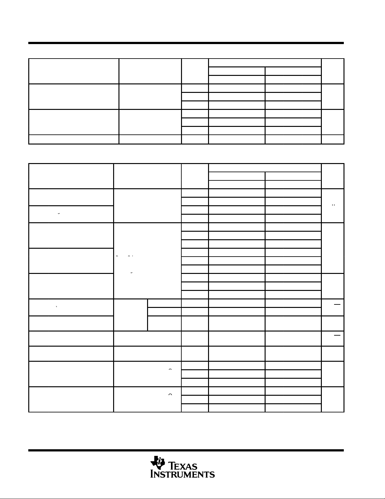
TL05x, TL05xA
A
ratio (∆V
CC±
/∆VIO)
(two am lifiers)
A
SR+Slew rate at unity gain
V/µs
SR
g
ns
()
C
L
100 F
g
g
V
q
V/√H
C
L
See Figure 4
Ph
V
10 mV
R
2 kΩ
gain
C
L
See Figure 4
ENHANCED-JFET LOW-OFFSET
OPERATIONAL AMPLIFIERS
SLOS178A – FEBRUARY 1997 - REVISED FEBRUARY 2003
TL052C and TL052AC electrical characteristics at specified free-air temperature (continued)
TL052C, TL052AC
k
SVR
I
CC
VO1/V
PARAMETER TEST CONDITIONS
Supply-voltage rejection
Supply current
p
Crosstalk attenuation AVD = 100 25°C 120 120 dB
O2
VO = 0, RS = 50 Ω
VO = 0, No load
T
A
25°C 75 99 75 99
0°C
70°C 75 97 75 97
25°C 4.6 5.6 4.8 5.6
0°C
70°C 4.4 6.4 4.6 6.4
V
= ±5 V V
CC±
MIN TYP MAX MIN TYP MAX
75 98 75 98
4.7 6.4 4.8 6.4
CC±
= ±15 V
TL052C and TL052AC operating characteristics at specified free-air temperature
TL052C, TL052AC
PARAMETER TEST CONDITIONS
RL = 2 kΩ, CL = 100 pF,
Negative slew rate
–
at unity gain
t
r
t
f
V
I
n
THD Total harmonic distortion
B
φ
†
Full range is 0°C to 70°C.
‡
For V
§
This parameter is tested on a sample basis. For other test requirements, please contact the factory. This statement has no bearing on testing
or nontesting of other parameters.
¶
For V
Rise time
Fall time
Overshoot factor
Equivalent input noise
n
voltage
Peak-to-peak equivalent
N(PP)
input noise current
Equivalent input
noise current
Unity-gain bandwidth
1
m
ase margin at unity
= ±5 V, V
CC±
= ±5 V, V
CC±
§
‡
= ±1 V; for V
I(PP)
O(RMS)
= 1 V; for V
See Figure 1
V
= ±10 mV ,
I(PP)
RL = 2 kΩ,
See Fi
RS = 20 Ω,
See Figure 3
f = 1 kHz 25°C 0.01 0.01 pA/√Hz
RS = 1 kΩ,
¶
f = 1 kHz
VI = 10 mV,
CC±
=
= 25 F,
=
I
= 25 F,
=
= ±15 V, V
= ±15 V, V
CC±
p
,
ures 1 and 2
f = 10 Hz 25°C 71 71
f = 1 kHz 25°C 19 19 30
f = 10 Hz to
10 kHz
RL = 2 kΩ,
RL = 2 kΩ,
p
,
p
I(PP)
=
L
= ±5 V.
O(RMS)
,
= 6 V.
†
T
A
25°C 17.8 9 20.7
Full range
25°C 15.4 9 17.8
Full range 8
25°C 55 56
0°C 54 55
70°C 63 63
25°C 55 57
0°C 54 56
70°C 62 64
25°C 24 19
0°C 24 19
70°C 24 19
25°C 4 4 µV
25°C 0.003 0.003 %
25°C 3 3
0°C 3.2 3.2
70°C 2.6 2.7
25°C 60 63
0°C 59 63
70°C 60 63
V
= ±5 V V
CC±
MIN TYP MAX MIN TYP MAX
CC±
8
= ±15 V
UNIT
dB
mA
UNIT
%
n
MHz
deg
z
10
POST OFFICE BOX 655303 • DALLAS, TEXAS 75265
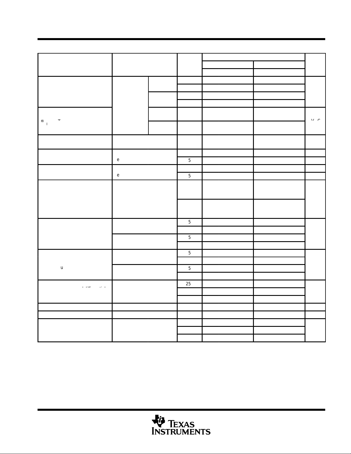
A
TL052I
VIOInput offset voltage
mV
V
0
TL052AI
V
IC
a
T
fficient
‡
V/°C
IIOInput offset current
O
,
IC
,
IIBInput bias current
O
,
IC
,
V
V
R
10 kΩ
V
V
R
2 kΩ
R
10 kΩ
V
g
V
R
2 kΩ
¶
voltage am lification
¶
C
V
V
i
rejection ratio
V
O
TL05x, TL05xA
ENHANCED-JFET LOW-OFFSET
OPERATIONAL AMPLIFIERS
SLOS178A – FEBRUARY 1997 - REVISED FEBRUARY 2003
TL052I and TL052AI electrical characteristics at specified free-air temperature
TL052I, TL052AI
PARAMETER TEST CONDITIONS
p
,
=
O
=
= 0,
RS = 50 Ω
emperature coe
V
IO
Input offset-voltage
long-term drift
p
p
Common-mode input
ICR
voltage range
Maximum positive peak
OM+
output voltage swing
Maximum negative peak
OM–
output voltage swing
A
r
c
CMRR
†
‡
§
¶
Large-signal differential
VD
Input resistance 25°C 10
i
Input capacitance 25°C 10 12 pF
i
ommon-mode
Full range is –40°C to 85°C.
This parameter is tested on a sample basis. For other test requirements, please contact the factory. This statement has no bearing on testing
or nontesting of other parameters
Typical values are based on the input offset-voltage shift observed through 168 hours of operating life test at TA = 150°C, extrapolated to
TA = 25°C using the Arrhenius equation, and assuming an activation energy of 0.96 eV .
At V
= ±5 V, VO = ±2.3 V; at V
CC±
§
p
VO = 0,
RS = 50 Ω
V
= 0, V
See Figure 5
V
= 0, V
See Figure 5
=
L
=
L
=
L
=
L
RL = 2 kΩ
=
IC
ICR
= 0,
=
= ±15 V, VO = ±10 V.
CC±
TL052I
TL052AI
VIC = 0, 25°C 0.04 0.04 µV/mo
= 0,
= 0,
n,
m
RS = 50 Ω
†
T
A
25°C 0.73 3.5 0.65 1.5
Full range 5.3 3.3
25°C 0.51 2.8 0.4 0.8
Full range 4.6 2.6
25°C to
85°C
25°C to
85°C
25°C 4 100 5 100 pA
85°C 0.06 10 0.07 10 nA
25°C 20 200 30 200 pA
85°C 0.6 20 0.7 20 nA
25°C
Full range
25°C 3 4.2 13 13.9
Full range 3 13
25°C 2.5 3.8 11.5 12.7
Full range 2.5 11.5
25°C –2.5 –3.5 –12 –13.2
Full range –2.5 –12
25°C –2.3 –3.2 –11 –12
Full range –2.3 –11
25°C 25 59 50 105
–40°C 30 74 60 145
85°C 20 43 30 76
25°C 65 85 75 93
–40°C 65 83 75 90
85°C 65 84 75 93
V
= ±5 V V
CC±
MIN TYP MAX MIN TYP MAX
7 6
6 6 25
–1
–2.3
to
to
4
5.6
–1
to
4
12
–11
–11
to
11
to
11
CC±
= ±15 V
–12.3
to
15.6
12
10
UNIT
µ
V/mV
Ω
dB
POST OFFICE BOX 655303 • DALLAS, TEXAS 75265
11
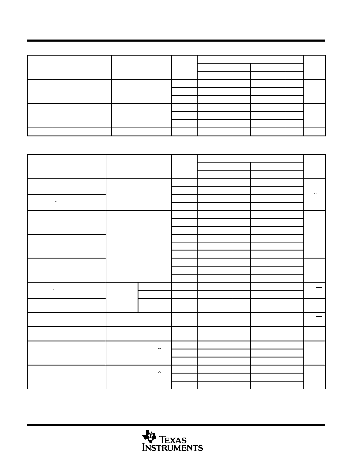
TL05x, TL05xA
A
ratio (∆V
CC±
/∆VIO)
(two am lifiers)
A
SR
Sl
‡
L
,
L
,
V/µs
SR
g
ns
V
I(PP)
±10 mV
V
q
V/√H
C
L
See Figure 4
Ph
V
10 mV
R
2 kΩ
gain
C
L
See Figure 4
ENHANCED-JFET LOW-OFFSET
OPERATIONAL AMPLIFIERS
SLOS178A – FEBRUARY 1997 - REVISED FEBRUARY 2003
TL052I and TL052AI electrical characteristics at specified free-air temperature (continued)
TL052I, TL052AI
k
SVR
I
CC
VO1/V
PARAMETER TEST CONDITIONS
Supply-voltage rejection
Supply current
p
Crosstalk attenuation AVD = 100 25°C 120 120 dB
O2
VO = 0, RS = 50 Ω
VO = 0, No load
T
A
25°C 75 99 75 99
–40°C
85°C 75 99 75 99
25°C 4.6 5.6 4.8 5.6
–40°C
85°C 4.4 6.4 4.6 6.4
V
= ±5 V V
CC±
MIN TYP MAX MIN TYP MAX
75 98 75 98
4.5 6.4 4.7 6.4
CC±
= ±15 V
TL052I and TL052AI operating characteristics at specified free-air temperature
TL052I, TL052AI
PARAMETER TEST CONDITIONS
+
ew rate at unity gain
Negative slew rate at
–
unity gain
t
r
t
f
V
I
n
THD Total harmonic distortion
B
φ
†
Full range is –40°C to 85°C.
‡
For V
§
This parameter is tested on a sample basis. For other test requirements, please contact the factory. This statement has no bearing on testing
or nontesting of other parameters.
¶
For V
Rise time
Fall time
Overshoot factor
Equivalent input noise
n
voltage
Peak-to-peak equivalent
N(PP)
input noise current
Equivalent input noise
current
Unity-gain bandwidth
1
m
CC±
CC±
‡
§
ase margin at unity
= ±5 V, V
= ±5 V, V
= ±1 V; for V
I(PP)
O(RMS)
= 1 V; for V
R
= 2 kΩ, C
See Figure 1
=
=
RL = 2 kΩ, CL = 100 pF,
See Figures 1 and 2
RS = 20 Ω,
See Figure 3
f = 1 kHz 25°C 0.01 0.01 pA/√Hz
RS = 1 kΩ,
¶
f = 1 kHz
VI = 10 mV,
= 25 F,
p
=
I
= 25 F,
=
p
= ±15 V, V
CC±
= ±15 V, V
CC±
= 100 pF,
,
f = 10 Hz 25°C 71 71
f = 1 kHz 25°C 19 19 30
f = 10 Hz to
10 kHz
RL = 2 kΩ,
RL = 2 kΩ,
,
I(PP)
=
L
O(RMS)
,
= ±5 V.
= 6 V.
†
T
A
25°C 17.8 9 20.7
Full range 8
25°C 15.4 9 17.8
Full range 8
25°C 55 56
–40°C 52 53
85°C 64 65
25°C 55 57
–40°C 51 53
85°C 64 65
25°C 24% 19%
–40°C 24% 19%
85°C 24% 19
25°C 4 4 µV
25°C 0.003 0.003 %
25°C 3 3
–40°C 3.5 3.6
85°C 2.5 2.6
25°C 60 63
–40°C 58 61
85°C 60 63
V
= ±5 V V
CC±
MIN TYP MAX MIN TYP MAX
CC±
= ±15 V
UNIT
dB
mA
UNIT
%
n
MHz
deg
z
12
POST OFFICE BOX 655303 • DALLAS, TEXAS 75265
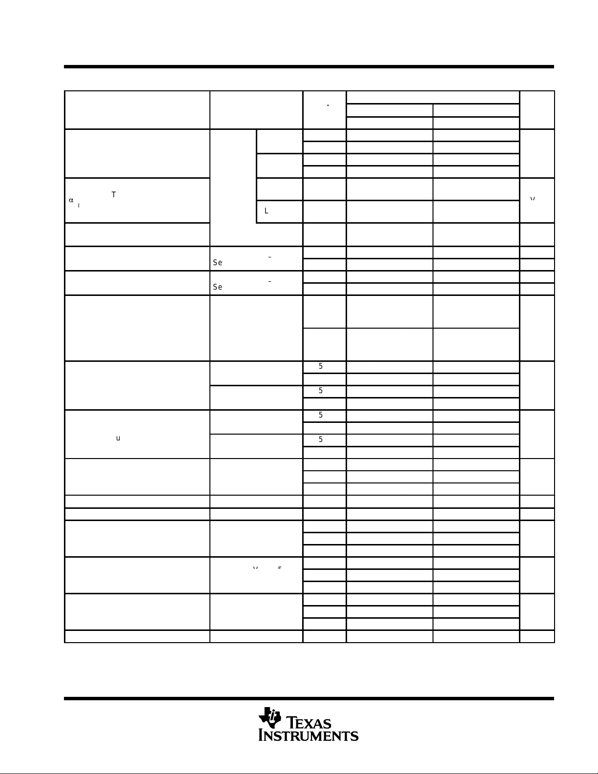
†
TL054C
VIOInput offset voltage
mV
TL054AC
V
O
a
R
S
Ω
V/°C
IIOInput offset current
OIC
IIBInput bias current
OIC
V
V
R
10 kΩ
V
V
R
2 kΩ
R
10 kΩ
V
g
V
R
2 kΩ
L
diff
l
voltage am lification
§
C
V
V
i
rejection ratio
V
O
R
S
Ω
S
V
±5 V to ±15 V
ratio (∆V
CC±
/∆VIO)
V
O
R
S
Ω
S
t
(four am lifiers)
TL05x, TL05xA
ENHANCED-JFET LOW-OFFSET
OPERATIONAL AMPLIFIERS
SLOS178A – FEBRUARY 1997 - REVISED FEBRUARY 2003
TL054C and TL054AC electrical characteristics at specified free-air temperature
TL054C, TL054AC
PARAMETER TEST CONDITIONS
p
= 0,
V
IO
ICR
OM+
OM–
A
VD
r
i
c
i
CMRR
k
SVR
I
CC
VO1/V
†
Full range is 0°C to 70°C.
‡
Typical values are based on the input offset-voltage shift observed through 168 hours of operating life test at TA = 150°C, extrapolated to
TA = 25°C using the Arrhenius equation, and assuming an activation energy of 0.96 eV .
§
For V
Temperature coefficient
of input offset voltage
Input offset-voltage
long-term drift
p
p
Common-mode input
voltage range
Maximum positive peak
output voltage swing
Maximum negative peak
output voltage swing
arge-signal
Input resistance 25°C
Input capacitance 25°C 10 12 pF
ommon-mode
upply-voltage rejection
upply curren
Crosstalk attenuation AVD = 100 25°C 120 120 dB
O2
= ±5 V, VO = ±2.3 V, at V
CC±
‡
erentia
p
p
VIC = 0,
= 50 Ω
50
R
VO = 0, VIC = 0,
See Figure 5
VO = 0, VIC = 0,
See Figure 5
=
L
=
L
=
L
=
L
RL = 2 kΩ 0°C 30 88 60 173 V/mV
=
IC
= 0,
CC±
= 0,
VO = 0, No load 0°C 8.2 12.8 8.5 12.8 mA
= ±15 V, VO = ±10 V.B
CC±
=
ICR
TL054C
TL054AC
n,
m
= 50
= 50
T
A
25°C 0.64 5.5 0.56 4
Full range 7.7 6.2
25°C 0.57 3.5 0.5 1.5
Full range 5.7 3.7
25°C to
70°C
25°C to
70°C
25°C 0.04 0.04 µV/mo
25°C 4 100 5 100 pA
70°C 0.02 1 0.025 1 nA
25°C 20 200 30 200 pA
70°C 0.15 4 0.2 4 nA
25°C
Full range
25°C 3 4.2 13 13.9
Full range 3 13
25°C 2.5 3.8 11.5 12.7
Full range 2.5 11.5
25°C –2.5 –3.5 –12 –13.2
Full range –2.5 –12
25°C –2.3 –3.2 –11 –12
Full range –2.3 –11
25°C 25 72 50 133
70°C 20 57 30 85
25°C 65 84 75 92
0°C 65 84 75 92 dB
70°C 65 84 75 93
25°C 75 99 75 99
,
0°C 75 99 75 99 dB
70°C 75 99 75 99
25°C 8.1 11.2 8.4 11.2
70°C 7.9 11.2 8.2 11.2
V
= ±5 V V
CC±
MIN TYP MAX MIN TYP MAX
25 23
24 23
–1
–2.3
to
–1
to
to
4
5.6
4
12
10
–11
–11
11
11
to
to
CC±
= ±15 V
–12.3
to
15.6
12
10
UNIT
µ
Ω
°
POST OFFICE BOX 655303 • DALLAS, TEXAS 75265
13
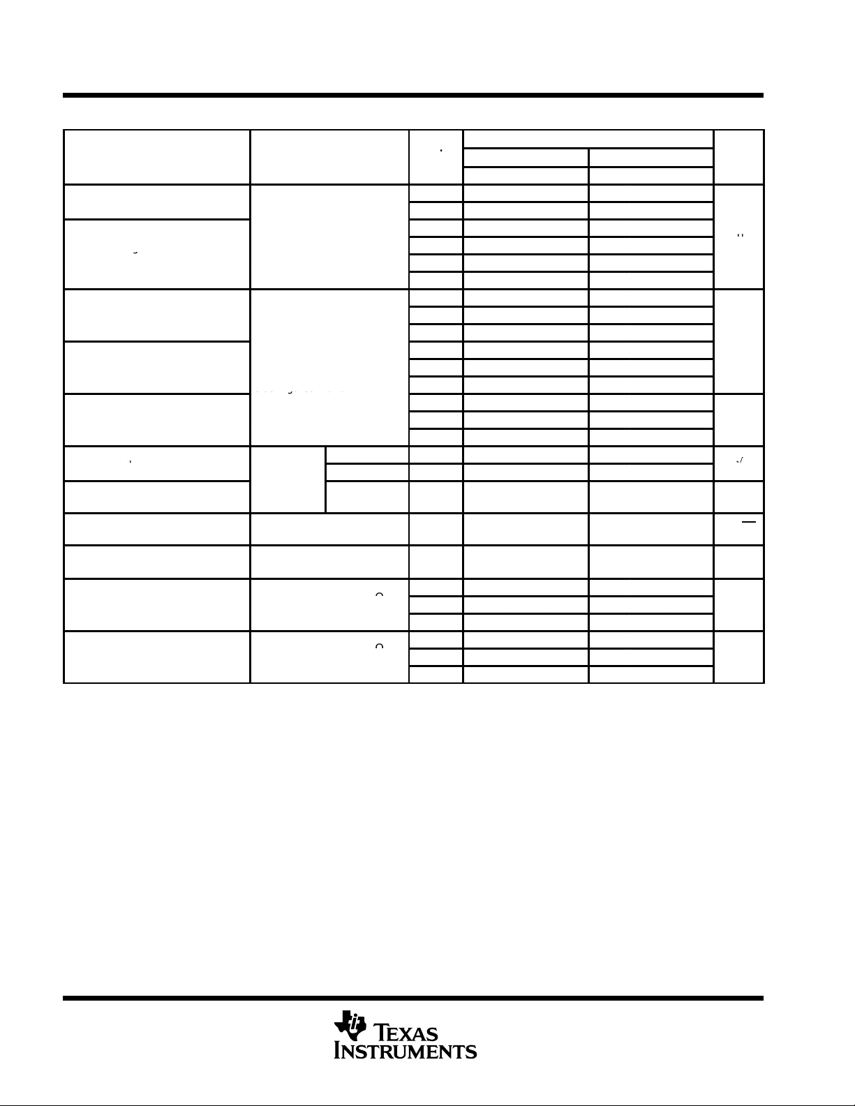
TL05x, TL05xA
†
SR
L L
V/µs
SR
g
ns
R
2 kΩ
C
L
100 F
g
See Figures 1 and 2
V
q
nV/√Hz
V
10 mV,R
2 kΩ
C
L
See Figure 4
Phase margin at
V
10 mV,R
2 kΩ
unity gain
C
L
See Figure 4
ENHANCED-JFET LOW-OFFSET
OPERATIONAL AMPLIFIERS
SLOS178A – FEBRUARY 1997 - REVISED FEBRUARY 2003
TL054C and TL054AC operating characteristics at specified free-air temperature
TL054C, TL054C
PARAMETER TEST CONDITIONS
Positive slew rate
+
at unity gain
RL = 2 kΩ,CL = 100 pF,
Negative slew rate at
–
unity gain
t
r
t
f
n
V
N(PP)
I
n
THD
B
1
φ
m
†
Full range is 0°C to 70°C.
‡
For V
§
This parameter is tested on a sample basis. For other test requirements, please contact the factory. This statement has no bearing on testing
or nontesting of other parameters.
¶
For V
Rise time 0°C 54 55
Fall time
Overshoot factor 0°C 24% 19%
Equivalent input noise
voltage
Peak-to-peak equivalent
input noise voltage
Equivalent input
noise current
Total harmonic
distortion
Unity-gain bandwidth
= ±5 V, V
CC±
= ±5 V, V
CC±
‡
§
¶
= ±1 V; for V
I(PP)
O(RMS
) = 1 V; for V
See Figure 1 and Note 7
V
= ±10 mV ,
I(PP)
See Fi
RS = 20 Ω,
See Figure 3
f = 1 kHz 25°C 0.01 0.01
RS = 1 kΩ,
f = 1 kHz
I
I
CC±
=
L
=
=
= 25 F,
=
= 25 F,
=
= ±15 V, V
CC±
,
p
,
ures 1 and 2
f = 10 Hz 25°C 75 75
f = 1 kHz 25°C 21 21 45
f = 10 Hz to
10 kHz
RL = 2 kΩ,
=
p
p
= ±15 V, V
L
=
L
I(PP)
O(RMS)
= ±5 V.
T
A
25°C 15.4 10 17.8
0°C 15.7 8 17.9
70°C 14.4 8 17.5
25°C 13.9 10 15.9
0°C 14.3 8 16.1
70°C 13.3 8 15.5
25°C 55 56
70°C 63 63
25°C 55 57
0°C 54 56
70°C 62 64
25°C 24% 19%
70°C 24% 19
25°C 4 4 µV
25°C 0.003 0.003 %
25°C 2.7 2.7
,
0°C 3 3 MHz
70°C 2.4 2.4
25°C 61 64
,
0°C 60 64 deg
70°C 61 63
= 6 V.
V
= ±5 V V
CC±
MIN TYP MAX MIN TYP MAX
CC±
= ±15 V
UNIT
%
pA/√Hz
14
POST OFFICE BOX 655303 • DALLAS, TEXAS 75265
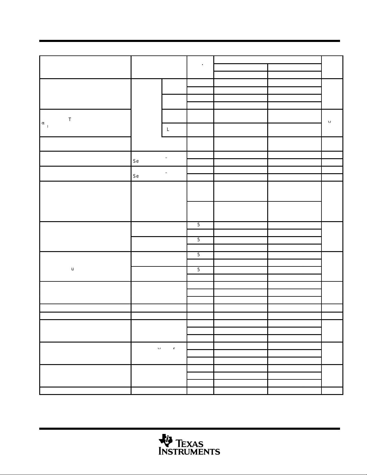
†
A
TL054I
VIOIn ut offset voltage
mV
TL054AI
V
O
R
S
Ω
V/°C
IIOInput offset current
OIC
IIBInput bias current
OIC
V
V
R
10 kΩ
V
V
R
2 kΩ
R
10 kΩ
V
g
V
R
2 kΩ
L
diff
l
voltage am lification
§
C
V
V
i
rejection ratio
V
O
R
S
Ω
S
V
±5 V to ±15 V
ratio (∆V
CC±
/∆VIO)
V
O
R
S
Ω
S
t
(four am lifiers)
TL05x, TL05xA
ENHANCED-JFET LOW-OFFSET
OPERATIONAL AMPLIFIERS
SLOS178A – FEBRUARY 1997 - REVISED FEBRUARY 2003
TL054I and TL054AI electrical characteristics at specified free-air temperature
TL054I, TL054AI
PARAMETER TEST CONDITIONS
p
= 0,
a
V
IO
ICR
OM+
OM–
A
VD
r
i
c
i
CMRR
k
SVR
I
CC
VO1/V
†
Full range is –40°C to 85°C.
‡
Typical values are based on the input offset voltage shift observed through 168 hours of operating life test at TA = 150°C, extrapolated to
TA = 25°C using the Arrhenius equation, and assuming an activation energy of 0.96 eV .
§
For V
Temperature coefficient of
input offset voltage
Input offset voltage
long-term drift
p
p
Common-mode input
voltage range
Maximum positive peak
output voltage swing
Maximum negative peak
output voltage swing
arge-signal
Input resistance 25°C
Input capacitance 25°C 10 12 pF
ommon-mode
upply-voltage rejection
upply curren
Crosstalk attenuation AVD = 100 25°C 120 120 dB
O2
= ±5 V, VO = ±2.3 V, at V
CC±
‡
erentia
p
p
VIC = 0,
= 50 Ω
50
R
VO = 0, VIC = 0,
See Figure 5
VO = 0, VIC = 0,
See Figure 5
=
L
=
L
=
L
=
L
RL = 2 kΩ –40°C 30 101 60 212 V/mV
=
IC
= 0,
CC±
= 0,
VO = 0, No load –40°C 7.9 12.8 8.2 12.8 mA
= ±15 V, VO = ±10 V.
CC±
=
ICR
TL054I
TL054AI
n,
m
= 50
= 50
T
A
25°C
Full range 8.8 7.3
25°C 0.57 3.5 0.5 1.5
Full range 6.8 4.8
25°C to
85°C
25°C to
85°C
25°C 0.04 0.04 µV/mo
25°C 4 100 5 100 pA
85°C 0.06 10 0.07 10 nA
25°C 20 200 30 200 pA
85°C 0.6 20 0.7 20 nA
25°C
Full range
25°C 3 4.2 13 13.9
Full range 3 13
25°C 2.5 3.8 11.5 12.7
Full range 2.5 11.5
25°C –2.5 –3.5 –12 –13.2
Full range –2.5 –12
25°C –2.3 –3.2 –11 –12
Full range –2.3 –11
25°C 25 72 50 133
85°C 20 50 30 70
25°C 65 84 75 92
–40°C 65 83 75 92 dB
85°C 65 84 75 93
25°C 75 99 75 99
,
–40°C 75 98 75 99 dB
85°C 75 99 75 99
25°C 8.1 11.2 8.4 11.2
85°C 7.6 11.2 7.9 11.2
V
= ±5 V V
CC±
MIN TYP MAX MIN TYP MAX
0.64 5.5 0.56 4
25 24
25 23
–1
–2.3
to
–1
to
to
4
5.6
4
12
10
= ±15 V UNIT
CC±
–11
–12.3
to
to
11
15.6
–11
to
11
12
10
µ
°
Ω
POST OFFICE BOX 655303 • DALLAS, TEXAS 75265
15

TL05x, TL05xA
†
A
SR
L L
V/µs
SR
g
,
ns
V
I(PP)
±10 mV, R
L
kΩ,
V
q
nV/√Hz
V
10 mV,R
2 kΩ
C
L
See Figure 4
Phase margin at
V
10 mV,R
2 kΩ
unity gain
C
L
See Figure 4
ENHANCED-JFET LOW-OFFSET
OPERATIONAL AMPLIFIERS
SLOS178A – FEBRUARY 1997 - REVISED FEBRUARY 2003
TL054I and TL054AI operating characteristics at specified free-air temperature
TL054I, TL054AI
PARAMETER TEST CONDITIONS
Positive slew rate
+
at unity gain
RL = 2 kΩ,CL = 100 pF,
Negative slew rate at
–
unity gain
t
r
t
f
n
V
N(PP)
I
n
THD
B
1
φ
m
†
Full range is –40°C to 85°C.
‡
For V
§
This parameter is tested on a sample basis. For other test requirements, please contact the factory. This statement has no bearing on testing
or nontesting of other parameters.
¶
For V
Rise time –40°C 52 53
Fall time
Overshoot factor –40°C 24 19
Equivalent input noise
voltage
Peak-to-peak equivalent
input noise voltage
Equivalent input
noise current
Total harmonic distortion
Unity-gain bandwidth
= ±5 V, V
CC±
= ±5 V, V
CC±
‡
§
= ±1 V; for V
I(PP)
O(RMS)
= 1 V; for V
See Figure 1
= ±10 mV, R
V
CL = 100 pF,
See Figures 1 and 2
RS = 20 Ω,
See Figure 3
f = 1 kHz 25°C 0.01 0.01 pA/√Hz
RS = 1 kΩ,
¶
f = 1 kHz
=
I
= 25 F,
p
=
I
=
p
= 25 F,
= ±15 V, V
CC±
= ±15 V, V
CC±
= 2 kΩ
2
f = 10 Hz 25°C 75 75
f = 1 kHz 25°C 21 21 45
f = 10 Hz to
10 kHz
RL = 2 kΩ,
=
L
=
L
= ±5 V.
I(PP)
O(RMS)
T
A
25°C 15.4 10 17.8
–40°C 16.4 8 18
85°C 14 8 17.3
25°C 13.9 10 15.9
–40°C 14.7 8 16.1
85°C 13 8 15.3
25°C 55 56
85°C 64 65
25°C 55 57
–40°C 51 53
85°C 64 65
25°C 24 19
85°C 24 19
25°C 4 4 µV
25°C 0.003% 0.003% %
25°C 2.7 2.7
,
–40°C 3.3 3.3 MHz
85°C 2.3 2.4
25°C 61 64
,
–40°C 59 62 deg
85°C 61 64
= 6 V.
V
= ±5 V V
CC±
MIN TYP MAX MIN TYP MAX
= ±15 V UNIT
CC±
%
16
POST OFFICE BOX 655303 • DALLAS, TEXAS 75265
TL05x, TL05xA
ENHANCED-JFET LOW-OFFSET
OPERATIONAL AMPLIFIERS
SLOS178A – FEBRUARY 1997 - REVISED FEBRUARY 2003
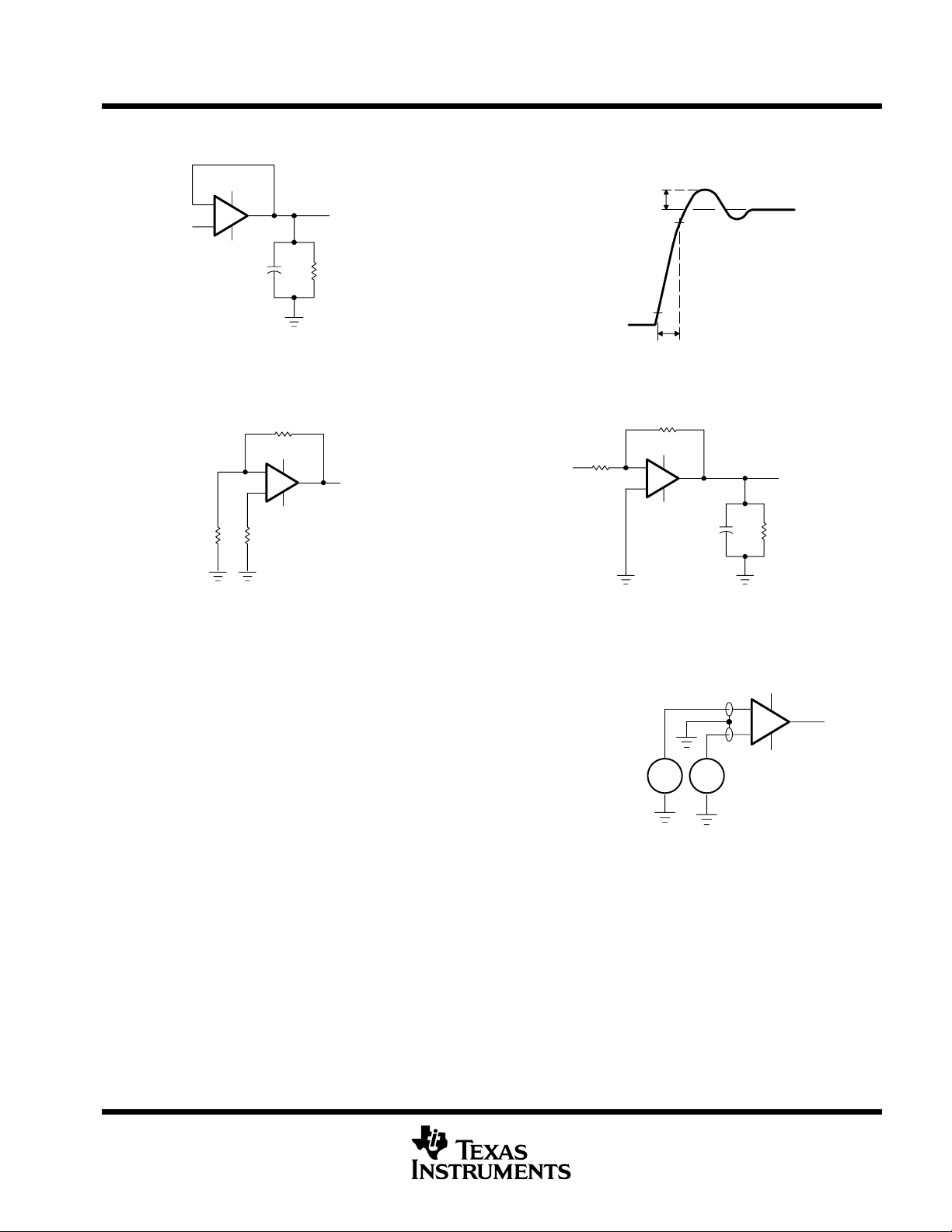
PARAMETER MEASUREMENT INFORMATION
V
CC+
–
V
NOTE A: CL includes fixture capacitance.
+
I
V
CC–
(see Note A)
C
L
V
O
R
L
Figure 1. Slew Rate, Rise/Fall Time,
and Overshoot Test Circuit
Overshoot
90%
10%
t
r
Figure 2. Rise-Time and Overshoot
Waveform
2 kΩ
V
CC+
–
+
V
CC–
R
S
R
S
V
O
V
I
100 Ω
NOTE A: CL includes fixture capacitance.
10 kΩ
V
CC+
–
+
V
CC–
(see Note A)
C
V
L
R
L
Figure 4. Unity-Gain Bandwidth and
Figure 3. Noise-Voltage Test Circuit
typical values
Typical values, as presented in this data sheet
Phase-Margin Test Circuit
Ground Shield
V
–
+
CC+
represent the median (50% point) of device
parametric performance.
pA pA
V
CC–
input bias and offset current
At the picoamp-bias-current level typical of the
TL05x and TL05xA, accurate measurement of the
bias current becomes difficult. Not only does this
Figure 5. Input-Bias and Offset-Current Test Circuit
measurement require a picoammeter, but
test-socket leakages easily can exceed the actual device bias currents. To accurately measure these small
currents, Texas Instruments uses a two-step process. The socket leakage is measured using picoammeters
with bias voltages applied, but with no device in the socket. The device then is inserted in the socket, and a
second test that measures both the socket leakage and the device input bias current is performed. The two
measurements then are subtracted algebraically to determine the bias current of the device.
noise
Because of the increasing emphasis on low noise levels in many of today’s applications, the input noise voltage
density is sample tested at f = 1 kHz. Texas Instruments also has additional noise-testing capability to meet
specific application requirements. Please contact the factory for details.
O
POST OFFICE BOX 655303 • DALLAS, TEXAS 75265
17
TL05x, TL05xA
ENHANCED-JFET LOW-OFFSET
OPERATIONAL AMPLIFIERS
SLOS178A – FEBRUARY 1997 - REVISED FEBRUARY 2003
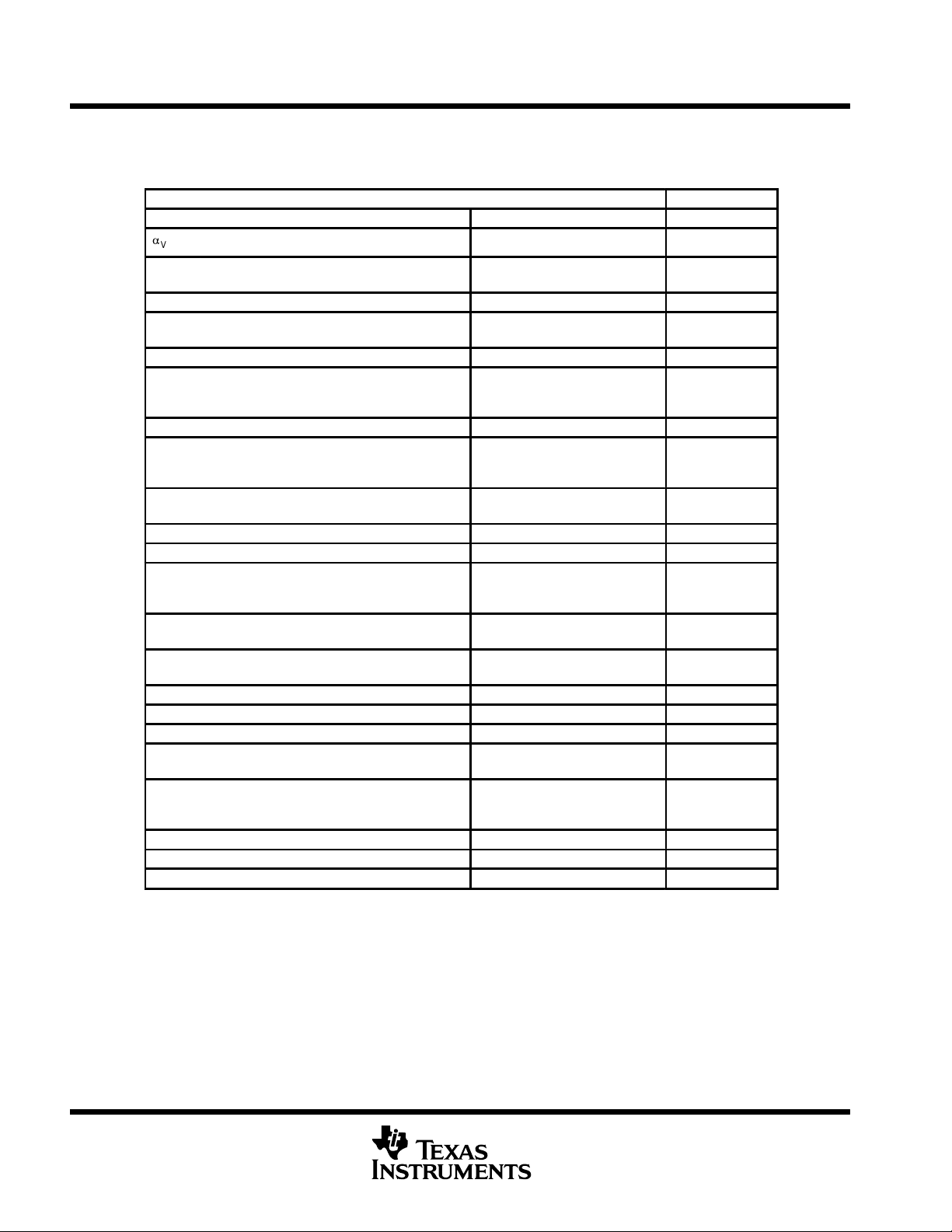
TYPICAL CHARACTERISTICS
V
IO
a
I
IB
I
IO
V
IC
V
O
V
OM
V
O(PP)
A
VD
CMRR Common-mode rejection ratio
z
o
k
SVR
I
OS
I
CC
SR Slew rate
V
n
THD Total harmonic distortion vs Frequency 63
B
1
φ
m
Input offset voltage Distribution 6–11
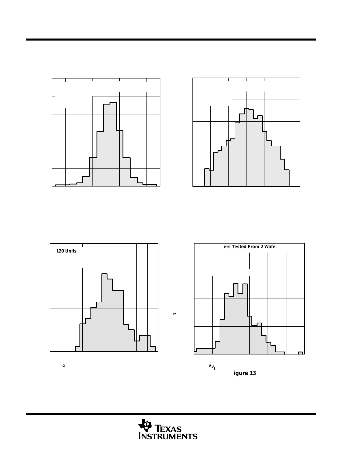
Temperature coefficient of input offset voltage Distribution 12, 13, 14
V
IO
Input bias current
Input offset current vs Free-air temperature 16
Common-mode input voltage range limits
Output voltage vs Differential input voltage 19, 20
Maximum peak output voltage
Maximum peak-to-peak output voltage vs Frequency 22, 23, 24
Large-signal differential voltage amplification
Output impedance vs Frequency 37
Supply-voltage rejection ratio vs Free-air temperature 38
Short-circuit output current
Supply current
Overshoot factor vs Load capacitance 60
Equivalent input noise voltage vs Frequency 61, 62
Unity-gain bandwidth
Phase margin
Phase shift vs Frequency 30
Voltage-follower small-signal pulse response vs Time 79
Voltage-follower large-signal pulse response vs Time 80
Table of Graphs
vs Common-mode input voltage
vs Free-air temperature
vs Supply voltage
vs Free-air temperature
vs Supply voltage
vs Output current
vs Free-air temperature
vs Load resistance
vs Frequency
vs Free-air temperature
vs Frequency
vs Free-air temperature
vs Supply voltage
vs Time
vs Free-air temperature
vs Supply voltage
vs Free-air temperature
vs Load resistance
vs Free-air temperature
vs Supply voltage
vs Free-air temperature
vs Supply voltage
vs Load capacitance
vs Free-air temperature
FIGURE
15
16
17
18
21
25, 26
27, 28
29
30
31, 32, 33
34, 35
36
39
40
41
42, 43, 44
45, 46, 47
48–53
54–59
64, 65, 66
67, 68, 69
70, 71, 72
73, 74, 75
76, 77, 78
18
POST OFFICE BOX 655303 • DALLAS, TEXAS 75265
P
t
f
A
lifi
%
TL05x, TL05xA
ENHANCED-JFET LOW-OFFSET
OPERATIONAL AMPLIFIERS
SLOS178A – FEBRUARY 1997 - REVISED FEBRUARY 2003
TYPICAL CHARACTERISTICS
Percentage of Units – %
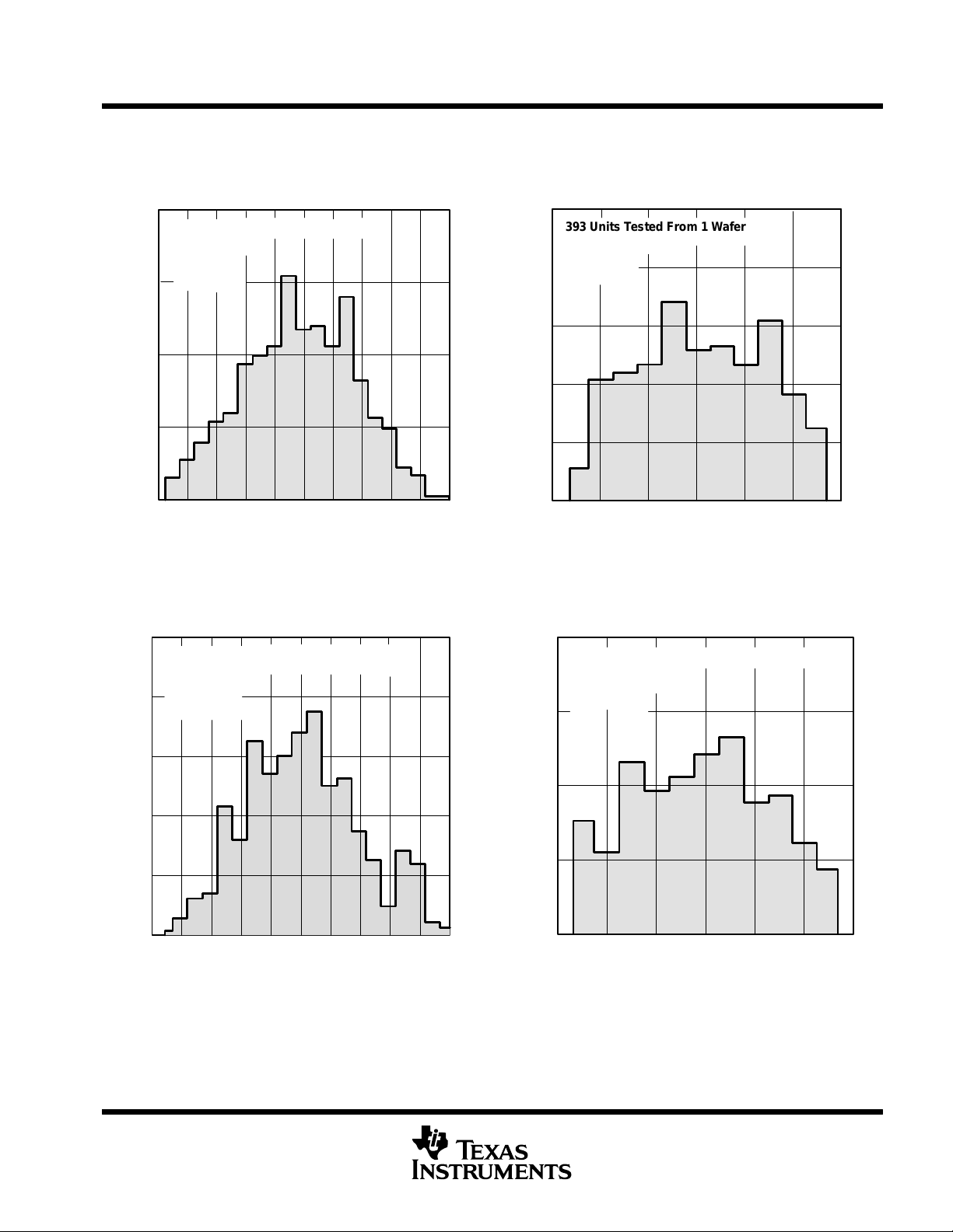
DISTRIBUTION OF TL051
INPUT OFFSET VOLTAGE
16
433 Units Tested From 1 Wafer Lot
V
= ±15 V
CC±
TA = 25°C
P Package
12
8
4
0
–1.5
–0.9 –0.3 0 0.3 0.9 1.5
–1.1 –0.6 0.6 1.1
VIO – Input Offset Voltage – mV
Figure 6
DISTRIBUTION OF TL052
INPUT OFFSET VOLTAGE
15
476 Amplifiers Tested From 1 Wafer Lot
V
= ±15 V
CC±
TA = 25°C
12
P Package
Percentage of Units – %
DISTRIBUTION OF TL051A
INPUT OFFSET VOLTAGE
20
393 Units Tested From 1 Wafer Lot
V
= ±15 V
CC±
TA = 25°C
16
P Package
12
8
4
0
–900
VIO – Input Offset Voltage – µV
Figure 7
DISTRIBUTION OF TL052A
INPUT OFFSET VOLTAGE
20
403 Amplifiers Tested From 1 Wafer Lot
V
= ±15 V
CC±
TA = 25°C
P Package
15
9006003000–300–600
ers –
mp
age o
ercen
9
6
3
0
–1.5
–0.9 –0.3 0 0.3 0.9 1.5
–1.2 –0.6 0.6 1.2
VIO – Input Offset Voltage – mV
Figure 8
10
5
Percentage of Amplifiers – %
0
–900 –600 –300 0 300 600 900
POST OFFICE BOX 655303 • DALLAS, TEXAS 75265
VIO – Input Offset Voltage – µV
Figure 9
19
TL05x, TL05xA
ENHANCED-JFET LOW-OFFSET
OPERATIONAL AMPLIFIERS
SLOS178A – FEBRUARY 1997 - REVISED FEBRUARY 2003
TYPICAL CHARACTERISTICS
Percentage of Amplifiers – %
DISTRIBUTION OF TL054
INPUT OFFSET VOLTAGE
30
1140 Amplifiers Tested From 3 Wafer Lots
V
= ±15 V
CC±
25
TA = 25°C
N Package
20
15
10
5
0
–4
–2013–3 –124
VIO – Input Offset Voltage – mV
Figure 10
DISTRIBUTION OF TL051
INPUT OFFSET VOLTAGE
TEMPERATURE COEFFICIENT
20
120 Units Tested From 2 Wafer Lots
V
= ±15 V
CC±
TA = 25°C to 125°C
16
P Package
Percentage of Amplifiers – %
DISTRIBUTION OF TL054A
INPUT OFFSET VOLTAGE
15
1048 Amplifiers Tested From 3 Wafer Lots
V
= ±15 V
CC±
TA = 25°C
12
N Package
9
6
3
0
–1.8
VIO – Input Offset Voltage – mV
Figure 11
DISTRIBUTION OF TL052
INPUT OFFSET VOLTAGE
TEMPERATURE COEFFICIENT
20
172 Amplifiers Tested From 2 Wafer Lots
V
= ±15 V
CC±
TA = 25°C to 125°C
P Package
15
Outlier: One Unit at –34.6 µV/°C
1.81.20.60–0.6–1.2
20
Percentage of Units – %
12
8
4
0
–20 –15 –10 –5 0 510152025
–25
a
– Temperature Coefficient – µV/°C
V
IO
Figure 12
POST OFFICE BOX 655303 • DALLAS, TEXAS 75265
Percentage of Amplifiers – %
10
5
0
a
– Temperature Coefficient – µV/°C
V
IO
20100–10–20–30
30
Figure 13
TL05x, TL05xA
ENHANCED-JFET LOW-OFFSET
OPERATIONAL AMPLIFIERS
SLOS178A – FEBRUARY 1997 - REVISED FEBRUARY 2003
TYPICAL CHARACTERISTICS
Percentage of Amplifiers – %
50
40
30
20
10
0
–60
100
10
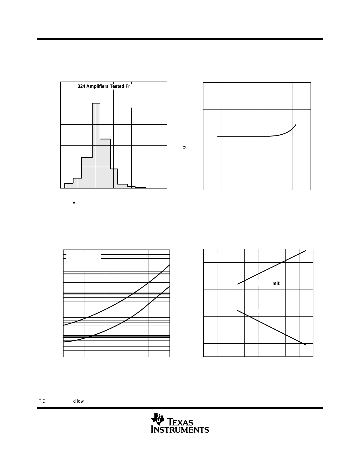
DISTRIBUTION OF TL054
INPUT OFFSET VOLTAGE
TEMPERATURE COEFFICIENT
324 Amplifiers Tested From 3 Wafer Lots
TA = 25°C to 125°C
–40 –20 0 20 40 60
– Temperature Coefficient – µV/°C
a
V
IO
Figure 14
INPUT BIAS CURRENT AND
INPUT OFFSET CURRENT
vs
FREE-AIR TEMPERATURE
V
= ±15 V
CC±
VO = 0
VIC = 0
I
1
IB
V
= ±15 V
CC±
N Package
†
INPUT BIAS CURRENT
vs
COMMON-MODE INPUT VOLTAGE
10
V
= ±15 V
CC±
TA = 25°C
5
0
– Input Bias Current – nA
IB
–5
I
–10
–15
–10 –5051015
VIC – Common-Mode Input Voltage – V
Figure 15
COMMON-MODE
INPUT VOLTAGE RANGE LIMITS
vs
16
TA = 25°C
12
8
4
SUPPLY VOLTAGE
Positive Limit
I
IO
I
I
– Input Bias and Offset Currents – nA
IO
and
IB
0.1
0.01
0.001
25
45 65 85 105 125
TA – Free-Air Temperature – °C
Figure 16
†
Data at high and low temperatures are applicable only within the rated operating free-air temperature ranges of the various devices.
POST OFFICE BOX 655303 • DALLAS, TEXAS 75265
0
Negative Limit
–4
–8
– Common-Mode Input Voltage – V
IC
–12
V
–16
2 4 6 8 10 12 14 16
0
|V
| – Supply Voltage – V
CC±
Figure 17
21
 Loading...