

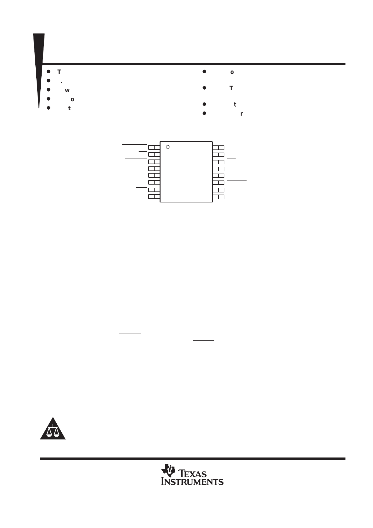
THMC50
REMOTE/LOCAL TEMPERATURE MONITOR AND
FAN CONTROLLER WITH SMBus INTERFACE
SLIS090 – JUL Y 1999
1
POST OFFICE BOX 655303 • DALLAS, TEXAS 75265
D
T wo-Wire SMBus Serial Interface
D
3.3 V Operation
D
Low Operating and Standby Current
D
Remote and Local Temperature Monitoring
D
0 V to 2.5 V, 8-bit DAC for Fan Speed
Control
D
Two Voltage Supervisors With Reset
Functions
D
Fault Tolerant Fan Control With Automatic
Hardware Trip Point
D
Bidirectional Thermal Overload Indicator
D
ACPI Thermal Model Compliant
1
2
3
4
5
6
7
8
16
15
14
13
12
11
10
9
FAN_OFF
MR
AUXRST
GND
VCC3AUX
VCC3
RST
FAN_SPD/NTEST_IN
SDA
SCL
INT
ADD/NTEST_OUT
GPI
THERM
REMOTE_DIODE+
REMOTE_DIODE–
16-Pin SSOP DBQ Package
(TOP VIEW)
NOTE: Pin assignments are preliminary.
description
The THMC50 is a local/remote temperature monitor with two voltage supervisor circuits and an 8-bit, 0-V to
2.5-V DAC designed for temperature monitoring and fan control via a two-wire SMBus serial interface. The
THMC50 is intended for use in personal computer applications according to the Advanced Configuration and
Power Interface (ACPI) thermal model. The device is also suitable for use in network routers and hubs, office
equipment, telephone switching networks, industrial control applications, and any other application requiring
temperature monitoring, fan speed control, and two 3.3-V supply voltage supervisors.
T emperature data is reported in a 2s complement, 8-bit binary format. The local temperature sensor can be used
to monitor the ambient temperature, while a remote thermal diode, such as the one present on the Intel
Pentium II, III, and the Sun UltraSPARC microprocessors, can be used to monitor the actual CPU die
temperature. For applications not using a microprocessor with an integrated thermal diode, an inexpensive
diode-connected 2N3904 NPN transistor can also be used to sense the remote temperature.
The THMC50 provides maskable interrupts for under/over temperature condition with default or user adjustable
limit values. If the temperature limit values are exceeded, the THMC50 asserts INT
low. If the default thermal
limits are exceeded, the THERM
terminal is asserted low, and the F AN_SPD analog output automatically goes
to full-scale voltage to set the fan at maximum speed. THERM
can also be used as an input to instantly command
full fan speed.
The 8-bit, 0–2.5 V DAC output of the THMC50, along with an external amplifier circuit, provides the means to
control the speed of a cooling fan. Fault tolerant fan-speed control is achieved through default and
user-programmable values for high temperature limits that command the fan to full speed once the temperature
limits are exceeded.
The THMC50 also provides two reset functions for the V
(VCC3AUX)
and V
(VCC3)
supply voltage. The reset
functions are assured down to 1-V supply voltage.
Copyright 1999, Texas Instruments Incorporated
PRODUCTION DATA information is current as of publication date.
Products conform to specifications per the terms of Texas Instruments
standard warranty. Production processing does not necessarily include
testing of all parameters.
Please be aware that an important notice concerning availability, standard warranty, and use in critical applications of
Texas Instruments semiconductor products and disclaimers thereto appears at the end of this data sheet.
Intel and Pentium are registered trademarks of Intel Corporation.
Sun is a registered trademark and UltraSPARC is a trademark of Sun Microsystems.
THMC50
REMOTE/LOCAL TEMPERATURE MONITOR AND
FAN CONTROLLER WITH SMBus INTERFACE
SLIS090 – JUL Y 1999
2
POST OFFICE BOX 655303 • DALLAS, TEXAS 75265
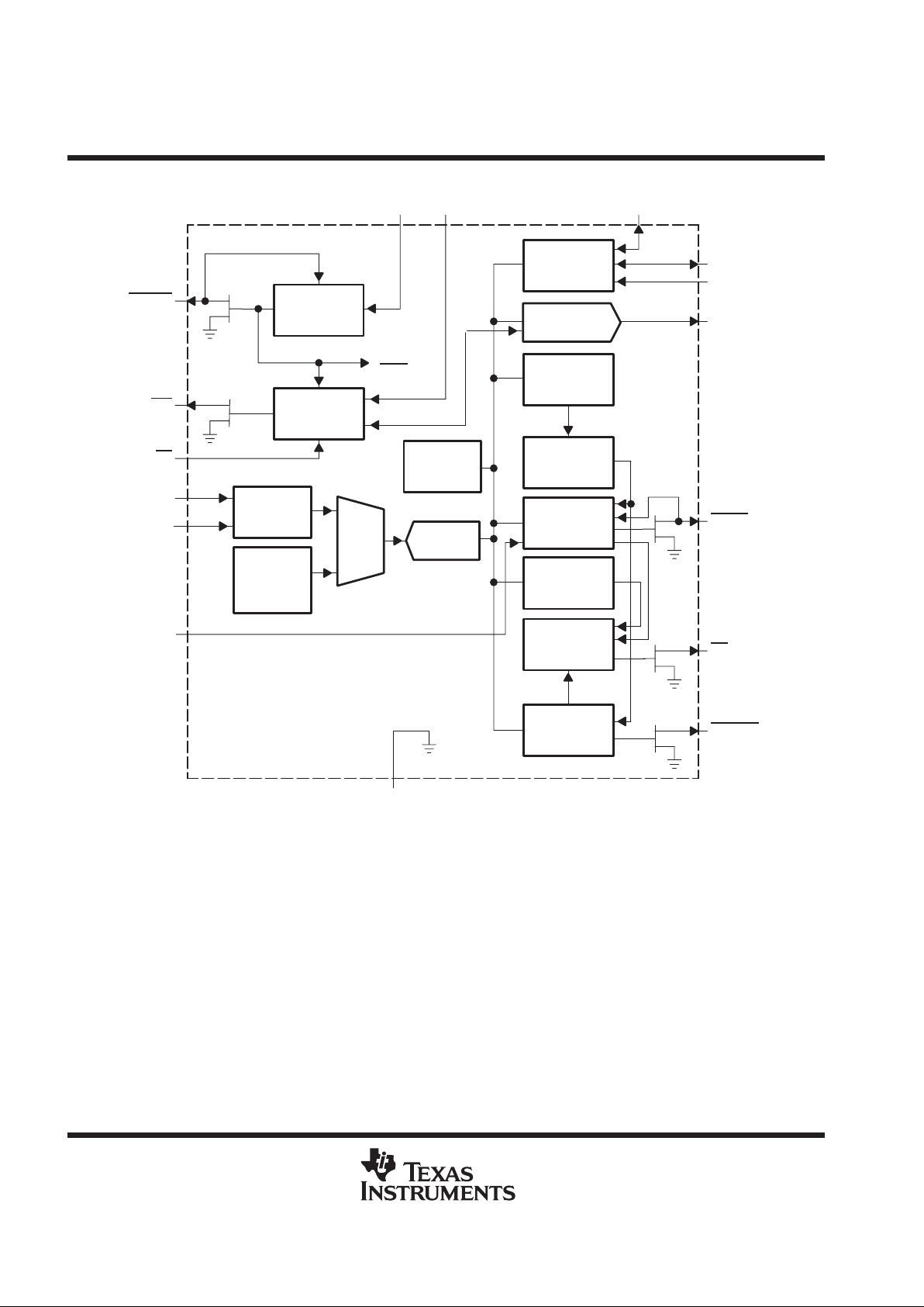
schematic/block diagram
ADC
Aux Reset
Generator
Bandgap
Temperature
Sensor
(Ambient)
Signal
Conditioning
Main Reset
Generator
Analog
Mux
SDA
Analog Output
Register & DAC
Configuration
Register
Mask
Gating
Interrupt
Mask
Register
Interrupt
Status
Registers
Limit
Comparators
Value & Limit
Registers
Serial Bus
Interface
GND
SCL
FAN_SPD/NTEST_IN
THERM
INT
FAN_OFF
AUXRST
RST
MR
REMOTE_DIODE+
REMOTE_DIODE–
GPI
VCC3AUX VCC3 ADD/NTEST_OUT
Address
Pointer
Register
Internal
Reset
THMC50
REMOTE/LOCAL TEMPERATURE MONITOR AND
FAN CONTROLLER WITH SMBus INTERFACE
SLIS090 – JUL Y 1999
3
POST OFFICE BOX 655303 • DALLAS, TEXAS 75265
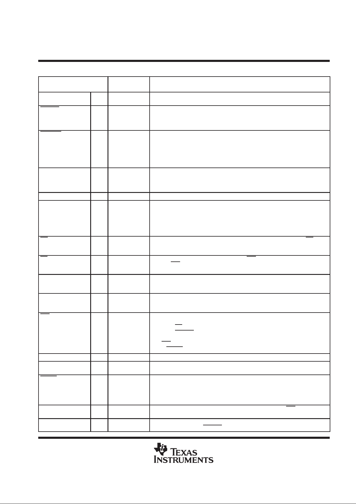
Terminal Functions
TERMINAL
NAME NO.
I/O
DESCRIPTION
ADD/NTEST_OUT 13 Digital I/O This terminal is used to determine the two LSBs of the SMBus address during initial
power on and it also functions as a digital output when doing a NAND tree test.
AUXRST 3 Digital I/O
(open drain)
This terminal is asserted low while VCC3AUX remains below the reset threshold. It
remains asserted for the reset timeout period after the reset condition is terminated. It is
bidirectional so that the THMC50 can be optionally reset; external logic must be used to
prevent a system auxiliary reset from occurring.
FAN_OFF 1 Digital output
(open drain)
Fan off request output. When commanded low via bit 5 in the configuration register
(0×40), this indicates a request to shut the fan off independent of the F AN_SPD output.
When commanded high via bit 5 in the configuration register (0×40), it indicates that the
fan may be turned on. This is an open-drain output requiring an external pullup.
Note: This terminal requires external circuitry to turn the fan off. It does not command the
analog output to 0×00 (see
Typical Application Schematic
).
FAN_SPD/NTEST_IN 8 Analog
output/test input
This terminal is an active-high input that enables NAND tree board-level connectivity
testing during device power up. Refer to the section on NAND tree testing. Also used as
the analog output of the 8-bit DAC for fan speed control when not in NAND tree test
mode.
GND 4 Ground
GPI 12 Digital input General-purpose input. The logic state of this terminal is reflected in bit 4 of the interrupt
status register (0x41). The logic state of the GPI terminal reported in bit 4 of the interrupt
status register (0x41) is inverted from the actual GPI logic state if bit 6 of the configuration
register (0x40) is set to a 1. If bit 6 of the configuration register (0×40) is set to a 0, then bit
4 of the interrupt status register (0×41) reports the same logic state present on the GPI
terminal.
INT 14 Digital output
(open drain)
System interrupt output. This signal indicates a violation of a set trip point. The INT output
is enabled when bit 1 of the configuration register (0x40) is set to 1. The default state is
disabled.
MR 2 Digital input Manual reset. A logic low on this input causes RST to be asserted. Once this input is
negated, RST
remains asserted for approximately 180 ms. This input has an internal
20-kΩ pullup resistor. Leave unconnected if not used.
REMOTE_DIODE– 9 Remote thermal
diode negative
input
This is the negative input (current sink) from the remote thermal diode.
REMOTE_DIODE+ 10 Remote thermal
diode positive
input
This is the positive input (current source) from the remote thermal diode.
RST 7 Digital output
(open drain)
This terminal is asserted low under any of the following conditions:
• VCC3 remains below the reset threshold
• While MR
is held low
• While AUXRST
is asserted
It remains asserted for the reset timeout period after the reset conditions are terminated.
The RST
function also resets the FAN_SPD analog output to 0xoo when asserted,
unless THERM
is asserted, then the FAN_SPD analog output will be 0xFF.
SCL 15 Digital input Serial SMBus clock
SDA 16 Digital I/O
(open drain)
Serial SMBus bidirectional data
THERM 11 Digital I/O
(open drain)
This is an active low thermal overload output that indicates a violation of a temperature
set point (overtemperature) for at least three monitoring cycles. Also acts as an input to
indicate a thermal event for fan control. When this signal is asserted low externally, a
status bit is set. The automatic fan control is activated to full on whenever this signal is
low.
VCC3 6 Analog input This is a 3.3-V main voltage monitor input for main reset generator (RST). This is not the
power supply terminal for THMC50.
VCC3AUX 5 Power supply
voltage input
This 3.3-V auxiliary voltage is the THMC50 power source and voltage monitor input for
auxiliary reset generator (AUXRST
). This terminal powers all THMC50 internal circuitry.
THMC50
REMOTE/LOCAL TEMPERATURE MONITOR AND
FAN CONTROLLER WITH SMBus INTERFACE
SLIS090 – JUL Y 1999
4
POST OFFICE BOX 655303 • DALLAS, TEXAS 75265
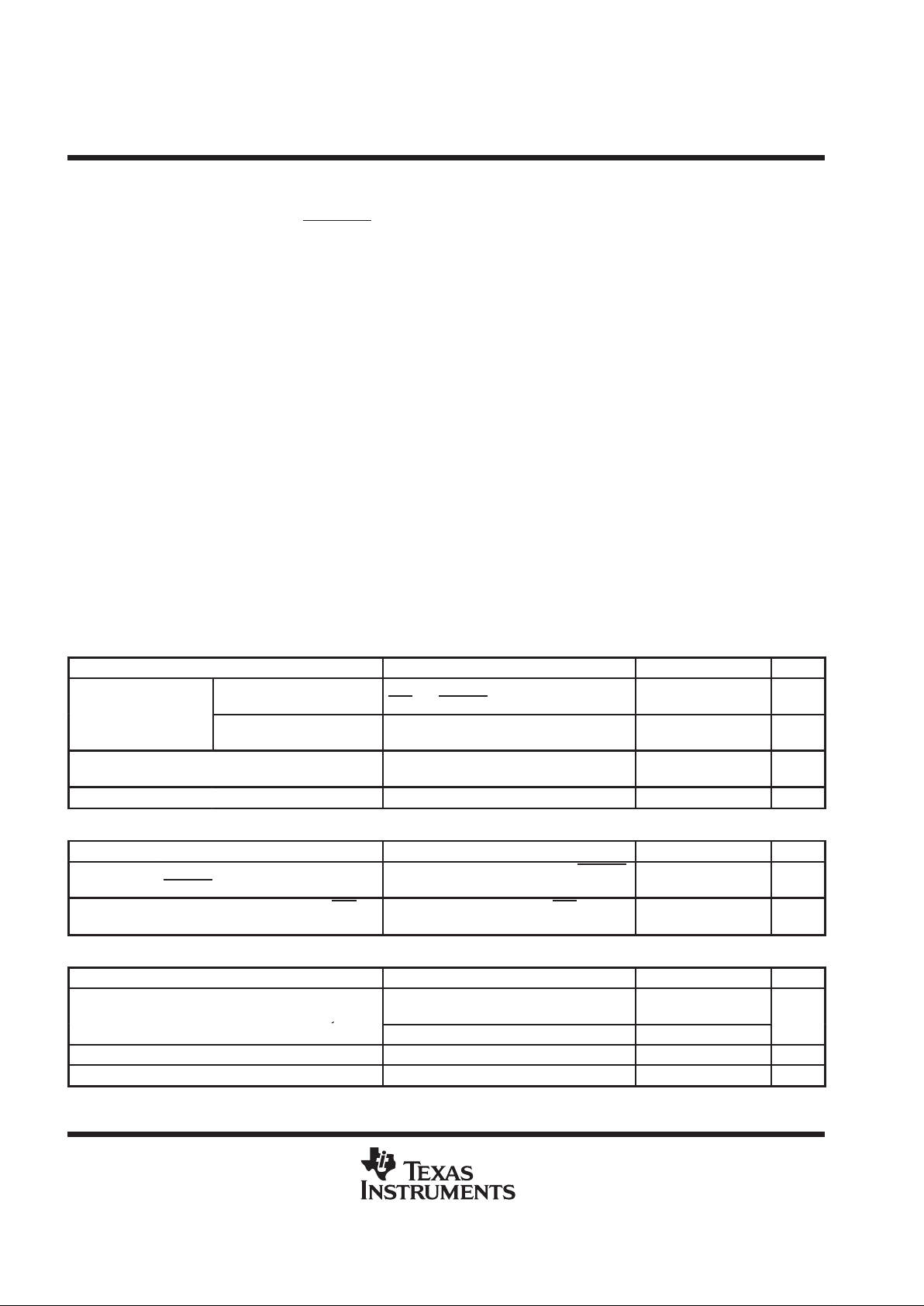
absolute maximum ratings over operating case temperature (see Note 1) (unless otherwise noted)
†
Voltage on VCC3AUX supply terminal, V
(VCC3AUX)
–0.3 V to 5.75 V. . . . . . . . . . . . . . . . . . . . . . . . . . . . . . . . . .
Maximum voltage allowed for FAN_OFF
pullup, V
(FAN_OFF)
5.5 V. . . . . . . . . . . . . . . . . . . . . . . . . . . . . . . . . . .
Input voltage on any I/O terminals (except analog inputs), V
(IOIN)
–0.3 V to V
(VCC3AUX)
+0.3 V. . . . . . . . . .
Input current on any I/O terminal (see Note 2), I
(IOIN)
–5 mA to 5 mA. . . . . . . . . . . . . . . . . . . . . . . . . . . . . . . . . .
Package input current (see Note 2), I
(PACKAGE)
–20 mA to 20 mA. . . . . . . . . . . . . . . . . . . . . . . . . . . . . . . . . . . .
Input voltage on REMOTE_DIODE– terminal,V
(REMOTE_DIODE–)
–0.3 V to 0.8 V. . . . . . . . . . . . . . . . . . . . . .
REMOTE_DIODE– input current, I
(REMOTE_DIODE–)
–1 mA to 1 mA. . . . . . . . . . . . . . . . . . . . . . . . . . . . . . . . .
Human body model ESD susceptibility, V
(HBMESD)
±2 kV. . . . . . . . . . . . . . . . . . . . . . . . . . . . . . . . . . . . . . . . . . .
Continuous power dissipation (see Note 3), P
D
330 mW. . . . . . . . . . . . . . . . . . . . . . . . . . . . . . . . . . . . . . . . . . . . .
Operating case temperature range, T
C
–40°C to 125°C. . . . . . . . . . . . . . . . . . . . . . . . . . . . . . . . . . . . . . . . . . . . .
Storage temperature (see Note 4), T
stg
–65°C to 165°C. . . . . . . . . . . . . . . . . . . . . . . . . . . . . . . . . . . . . . . . . . . . .
Junction temperature, T
J
150°C. . . . . . . . . . . . . . . . . . . . . . . . . . . . . . . . . . . . . . . . . . . . . . . . . . . . . . . . . . . . . . . . . .
Lead temperature (soldering, 10 sec), T
(LEAD)
300°C. . . . . . . . . . . . . . . . . . . . . . . . . . . . . . . . . . . . . . . . . . . . . . .
†
Stresses beyond those listed under “absolute maximum ratings” may cause permanent damage to the device. These are stress ratings only, and
functional operation of the device at these or any other conditions beyond those indicated under “recommended operating conditions” is not
implied. Exposure to absolute-maximum-rated conditions for extended periods may affect device reliability.
NOTES: 1. All voltages are measured with respect to GND, unless otherwise specified.
2. The 20-mA maximum package input current rating limits the number of terminals that can safely exceed the power supplies with
an input current of 5 mA to four terminals.
3. The maximum power dissipation must be derated at elevated temperatures and is dictated by T
Jmax
, θJA and the ambient
temperature, TA. The maximum allowable power dissipation at any temperature is PD = (T
Jmax
– TA)/θJA.
4. Solder accordingly to IPC standards.
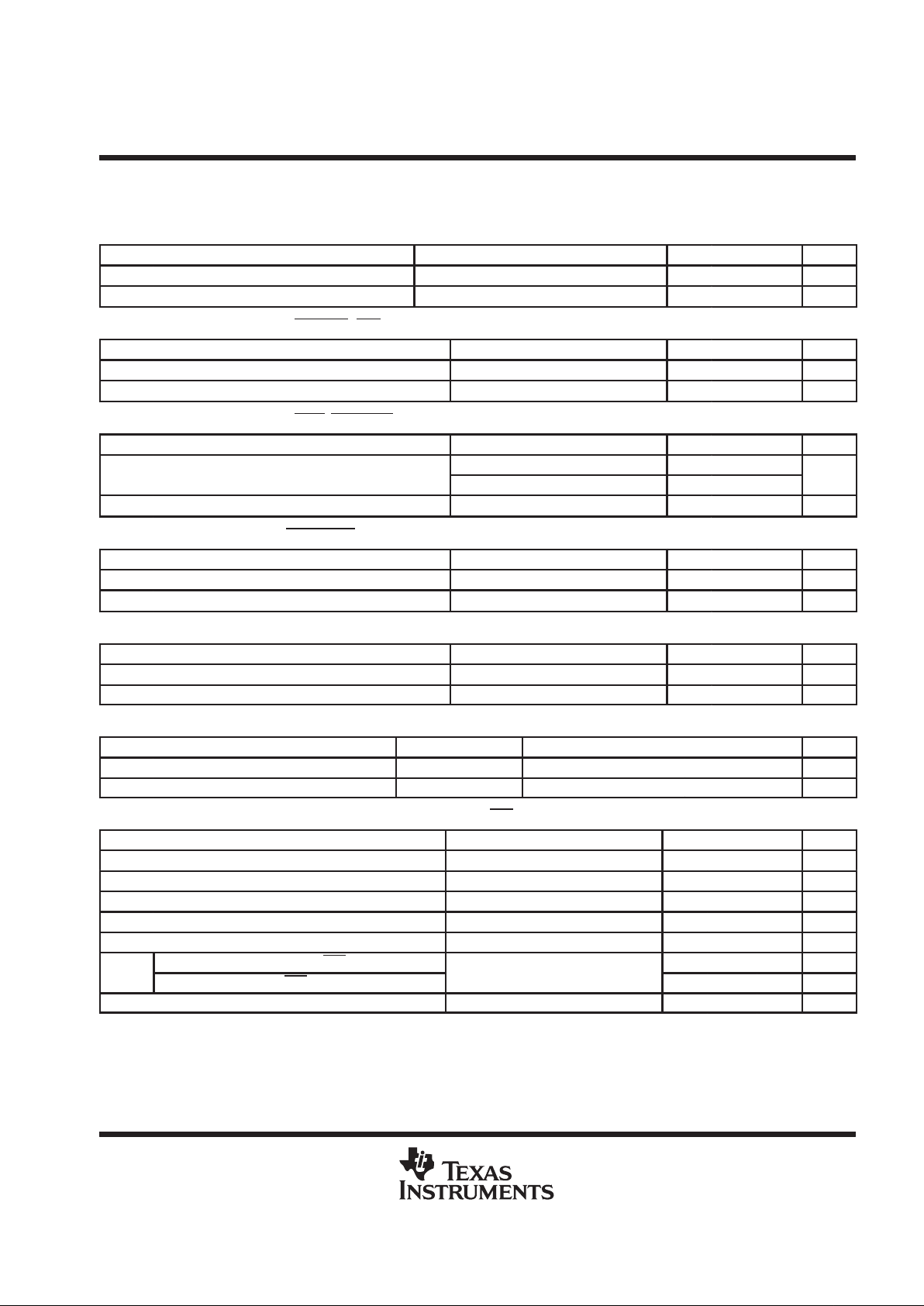
dc electrical characteristics, V
CC3
= V
(VCC3AUX)
= 3.3 V, TA = 25°C (unless otherwise noted)
power supply
PARAMETER TEST CONDITIONS MIN TYP MAX UNITS
VCC3AUX reset generator
supply voltage
Voltage on VCC3AUX needed to guarantee
RST
and AUXRST to stay valid
1 3.8 V
V
(VCC3AUX_RST)
VCC3AUX supply voltage
Normal operating supply voltage for all other
THMC50 circuits
3 3.3 3.8 V
I
(VCC3AUX)
Supply current
(interface inactive)
Exclude D/A converter source/sink current 1 2 mA
I
(VCC3AUX_STANDBY)
Standby mode 500 µA
voltage supervisors
PARAMETER TEST CONDITIONS MIN TYP MAX UNITS
V
THAUXRST
Threshold voltage on VCC3AUX for
AUXRST
active
Reduce VCC3AUX from 3.8 V until AUXRST
is low.
2.88 3 V
V
THRST
Threshold voltage on VCC3 for RST
active
Reduce VCC3 from 3.8 V until RST is low
with VCC3AUX = 3.3 V
2.88 3 V
temperature-to-digital converter
PARAMETER TEST CONDITIONS MIN TYP MAX UNITS
T
Measured temperature accurac
y
–40°C ≤TA < 60°C and
100°C <TA ≤ 125°C
–5 5
°C
(ACC)
y
60°C ≤TA ≤ 100°C –3 3
T
(RES)
Temperature resolution Design parameter – not tested 1 °C
V
(THRESH)
Remote_Diode+ open fault threshold 2.4 V
THMC50
REMOTE/LOCAL TEMPERATURE MONITOR AND
FAN CONTROLLER WITH SMBus INTERFACE
SLIS090 – JUL Y 1999
5
POST OFFICE BOX 655303 • DALLAS, TEXAS 75265
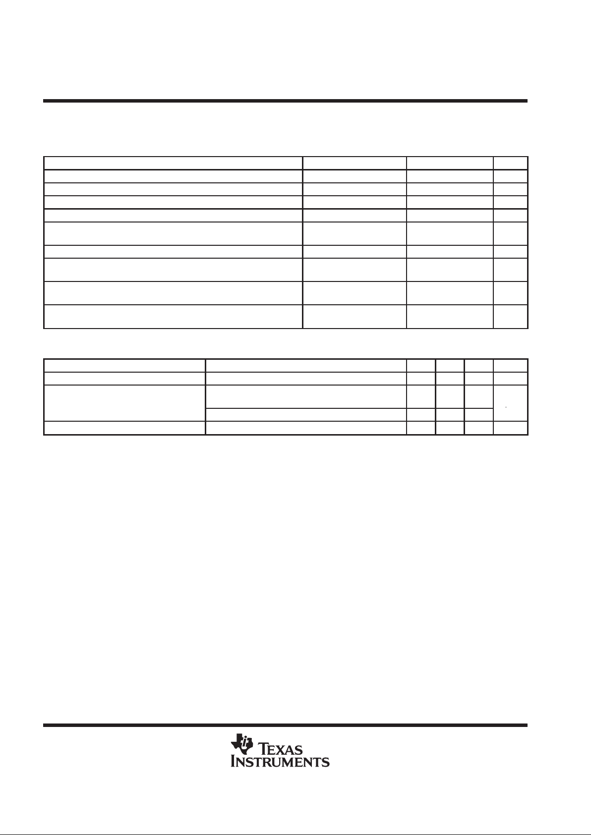
dc electrical characteristics, V
CC3
= V
(VCC3AUX)
= 3.3 V, TA = 25°C (unless otherwise noted)
(continued)
digital output: ADD/NTEST_OUT
PARAMETER TEST CONDITIONS MIN TYP MAX UNITS
V
OH
Logical 1 output voltage I
OUT
= –3 mA at V
(VCC3AUX)
= 2.85 V 2.4 V
V
OL
Logical 0 output voltage I
OUT
= 3 mA at V
(VCC3AUX)
= 3.8 V 0.4 V
open-drain digital outputs: THERM, INT
PARAMETER TEST CONDITIONS MIN TYP MAX UNITS
V
OL
Logical 0 output voltage I
OUT
= 3 mA at V
(VCC3AUX)
= 3.8 V 0.4 V
I
OH
High level output current V
OUT
= V
(VCC3AUX)
= 3.8 V 0.1 100 µA
open-drain digital outputs: RST, AUXRST
PARAMETER TEST CONDITIONS MIN TYP MAX UNITS
p
I
OUT
= 3 mA at V
(VCC3AUX)
= 3.8 V 0.4
VOLLogical 0 output voltage
I
OUT
= 3 mA at V
(VCC3AUX)
= 1 V 0.4
V
I
OH
High level output current V
OUT
= V
(VCC3AUX)
= 3.8 V 0.1 100 µA
open-drain digital output: FAN_OFF
PARAMETER TEST CONDITIONS MIN TYP MAX UNITS
V
OL
Logical 0 output voltage I
OUT
= 6 mA at V
(VCC3AUX)
= 3.8 V 0.4 V
I
OH
High level output current V
OUT
= V
(VCC3AUX)
= 3.8 V 0.1 100 µA
open-drain SMBus output: SDA
PARAMETER TEST CONDITIONS MIN TYP MAX UNITS
V
OL
Logical 0 output voltage I
OUT
= 3 mA at V
(VCC3AUX)
= 3.8 V 0.4 V
I
OH
High level output current V
OUT
= V
(VCC3AUX)
= 3.8 V 0.1 100 µA
SMBus digital inputs: SCL, SDA
PARAMETER TEST CONDITIONS MIN TYP MAX UNITS
V
IH
Logical 1 input voltage 0.7 × V
(VCC3AUX)
V
V
IL
Logical 0 input voltage 0.3 × V
(VCC3AUX)
V
digital inputs: FAN_SPD/NTEST_IN, ADD/NTEST_OUT, MR, GPI
PARAMETER TEST CONDITIONS MIN TYP MAX UNITS
V
IH
Logical 1 input voltage (5 V) 2.4 V
V
IL
Logical 0 input voltage (5 V) 0.8 V
V
IH
Logical 1 input voltage (3.3 V) 2 V
V
IL
Logical 0 input voltage (3.3 V) 0.4 V
I
IH
Logical 1 input current VIN = V
(VCC3AUX)
–0.005 –1 mA
Logical 0 input current (except MR)
0.005 1 mA
I
IL
Logical 0 input current (MR)
V
IN
=
0 V dc
165 250 µA
C
(IN)
Digital input terminal capacitance Design parameter only – not tested 20 pF
THMC50
REMOTE/LOCAL TEMPERATURE MONITOR AND
FAN CONTROLLER WITH SMBus INTERFACE
SLIS090 – JUL Y 1999
6
POST OFFICE BOX 655303 • DALLAS, TEXAS 75265
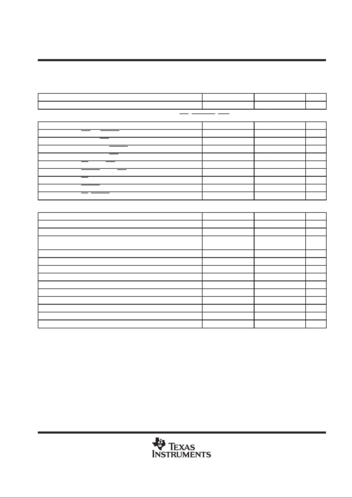
dc electrical characteristics, V
CC3
= V
(VCC3AUX)
= 3.3 V, TA = 25°C (unless otherwise noted)
(continued)
analog output: FAN_SPD/NTEST_IN
PARAMETER TEST CONDITIONS MIN TYP MAX UNITS
V
OUT
Output voltage range 0 2.5 V
Total unadjusted error (TUE) (see Note 5) IL = –2 mA –3% 3%
Full-scale error –3% ±1% 3%
Zero error, LSB No load 2
Differential nonlinearity (DNL), LSB (monotonic by design)
DAC setting
0 × 16 to 0 ×FF
–1 1
Integral nonlinearity , LSB ±1
C
(LOAD)
Maximum external load capacitance allow to insure DAC
stability
Design parameter only –
not tested
50 pF
I
(SOURCE)
Output source current
DAC setting
0 × 16 to 0 ×FF
–2 mA
I
(SINK)
Output sink current
DAC setting
0 × 16 to 0 ×FF
1 mA
NOTE 5: Total unadjusted error (TUE) includes offset, gain, and linearity errors of the DAC.
remote thermal diode sensing
PARAMETER TEST CONDITIONS MIN TYP MAX UNITS
T
(RES)
T emperature resolution 1 °C
I
Diode source current
REMOTE_DIODE+ = REMOTE_DIODE– + 0.65 V ,
high level
80 130
µ
A
(DIODE)
Low level 8 13
µ
I
(RATIO)
Diode source current ratio High level/low level 9.8 10 10.2
THMC50
REMOTE/LOCAL TEMPERATURE MONITOR AND
FAN CONTROLLER WITH SMBus INTERFACE
SLIS090 – JUL Y 1999
7
POST OFFICE BOX 655303 • DALLAS, TEXAS 75265
ac electrical characteristics, V
CC3
= V
(VCC3AUX)
= 3.3 V, TA = 25°C (see Notes 6 and 7) (unless
otherwise noted)
temperature-to-digital converter timing parameters: Remote_Diode+, Remote_Diode–
PARAMETER TEST CONDITIONS MIN TYP MAX UNITS
t
(SAMPLE)
T emperature-to-digital acquisition sample rate 0.75 1 1.25 sa/s
reset function timing parameters: VCC3, VCC3AUX, MR, AUXRST, RST
PARAMETER TEST CONDITIONS MIN TYP MAX UNITS
t
(RP)
RST and AUXRST pulse duration See Figures 17–20 140 560 ms
t
(VCC3RST)
VCC3 to RST delay See Figures 17–20 20 µs
t
(VCC3AUX1)
VCC3AUX to AUXRST delay See Figures 17–20 20 µs
t
(VCC3AUX2)
VCC3AUX to RST delay See Figures 17–20 20 µs
t
(MR)
MR input to RST delay See Figures 17–20 0.5 µs
t
(RST)
AUXRST input to RST delay See Figures 17–20 0.5 µs
t
(MRMIN)
MR input minimum pulse width 10 µs
t
(AUXRSTMIN)
AUXRST input minimum pulse width 10 µs
t
(GLITCH)
MR, AUXRST glitch immunity 100 ns
SMBus interface timing parameters: SCL, SDA
PARAMETER TEST CONDITIONS MIN TYP MAX UNITS
f
(SCL)
SCL operating frequency See Figure 1 10 100 kHz
t
(BUF)
Bus free time between stop and start condition See Figure 1 4.7 µs
t
(HDSTA)
Hold time after (repeated) start condition. After this period,
the first clock is generated
See Figure 1 4 µs
t
(SUSTA)
Repeated start condition setup time See Figure 1 4.7 µs
t
(SUSTO)
Stop condition setup time See Figure 1 4 µs
t
(HDDAT)
Data hold time See Figure 1 300 ns
t
(SUDAT)
Data setup time See Figure 1 250 ns
t
(LOW)
SCL clock low period See Figure 1 4.7 µs
t
(HIGH)
SCL clock high period See Figure 1 4 50 µs
t
(LOWSEXT)
Cumulative clock low extend time (slave device) See Figure 1 25 ms
t
(LOWMEXT)
Cumulative clock low extend time (master device) See Figure 1 10 ms
t
F
Clock/data fall time See Figure 1 300 ns
t
R
Clock/data rise time See Figure 1 1000 ns
NOTES: 6. Typicals are at TJ = TA = 25°C with V
(VCC3AUX)
= 3.3 V and represent most likely parametric norm.
7. Timing specifications are tested at the TTL logic levels, VIL = 0.4 V for a falling edge and VIH = 2.4 V for a rising edge. The 3-state
output voltage is forced to 1.4 V.
THMC50
REMOTE/LOCAL TEMPERATURE MONITOR AND
FAN CONTROLLER WITH SMBus INTERFACE
SLIS090 – JUL Y 1999
8
POST OFFICE BOX 655303 • DALLAS, TEXAS 75265
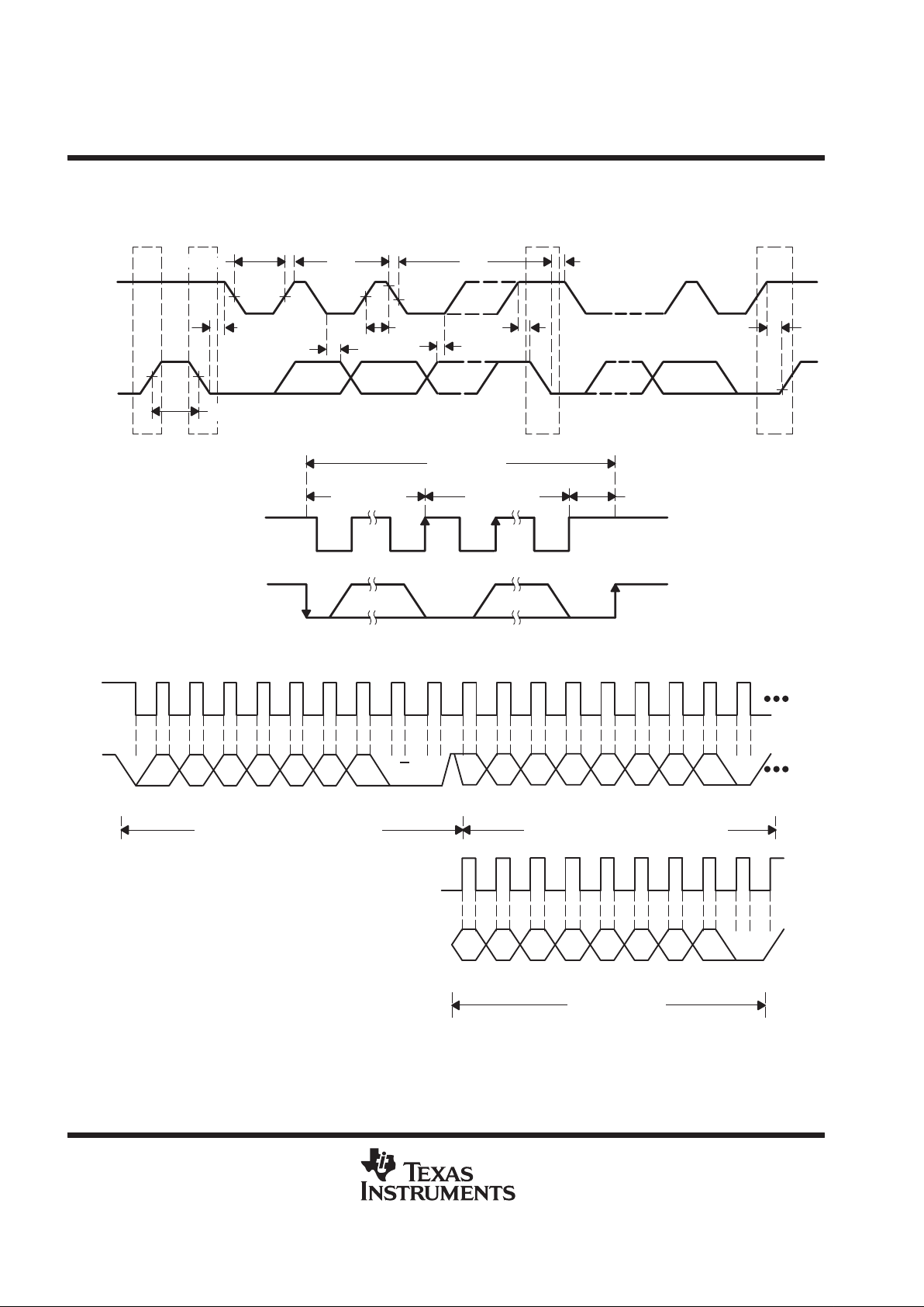
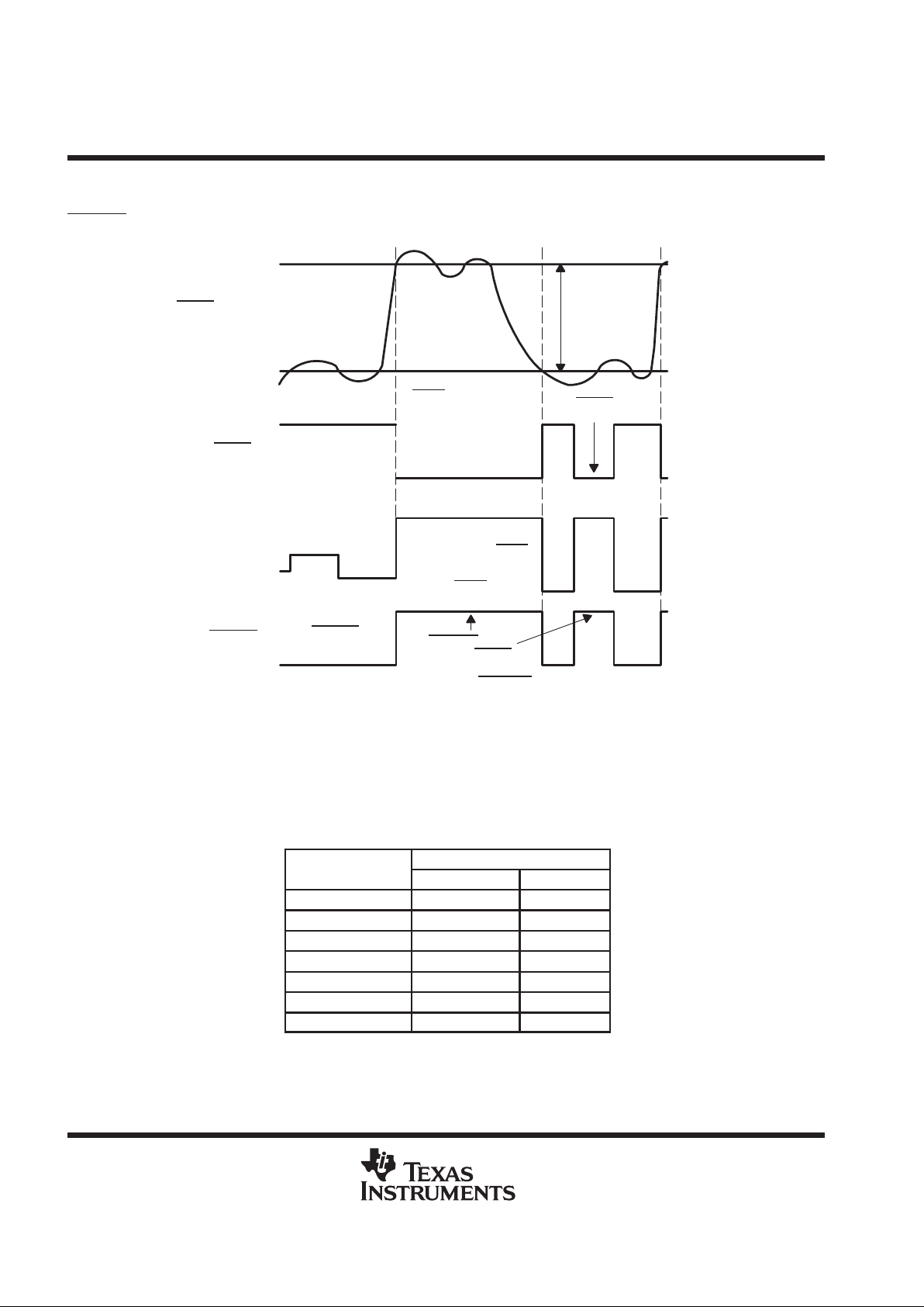
PARAMETER MEASUREMENT INFORMATION
SMBus timing diagrams
PS
t
(HDSTA)
t
(HDDAT)
t
(HIGH)
t
(SUDAT)
t
(SUSTA)
t
(HDSTA)
t
(SUSTO)
SP
SCLK
SDATA
Start
Stop
SCLK
ACK
SCLK
ACK
t
(LOWMEXT)
SCLK
SDATA
t
(LOW)
t
(LOWSEXT)
t
F
t
R
t
(BUF)
t
(LOWMEXT)
t
(LOWMEXT)
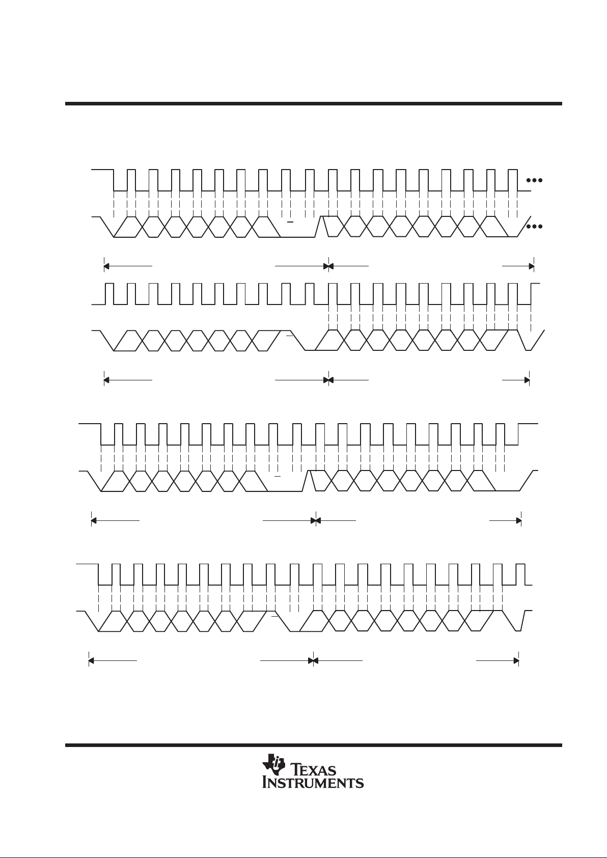
Figure 1. SMBus Timing Diagram
Frame 3 Data Byte
Frame 1 SMBus Slave Address Byte
Frame 2 Address Pointer Register Byte
A6 A5 A4 A3 A2 A1 A0 D7 D6 D5 D4 D3 D2 D1 D0R/W
SCLK
SDATA
Start By
Master
ACK By
THMC50
ACK By
Master
D7 D6 D5 D4 D3 D2 D1 D0
ACK By
THMC50
Stop By
Master
SCLK
(Continued)
SDATA
(Continued)
1
91 9
19
Figure 2. SMBus Timing Diagram for Write Byte Format
THMC50
REMOTE/LOCAL TEMPERATURE MONITOR AND
FAN CONTROLLER WITH SMBus INTERFACE
SLIS090 – JUL Y 1999
9
POST OFFICE BOX 655303 • DALLAS, TEXAS 75265
PARAMETER MEASUREMENT INFORMATION
SMBus timing diagrams (continued)
Frame 1 SMBus Slave Address Byte
Frame 2 Address Pointer Register Byte
A6 A5 A4 A3 A2 A1 A0 D7 D6 D5 D4 D3 D2 D1 D0R/W
SCLK
SDATA
Start By
Master
ACK By
THMC50
ACK By
Master
SCLK
(Continued)
SDATA
(Continued)
1
91 9
Frame 3 SMBus Slave Address Byte
Frame 4 Data Byte Read From THMC50
A6 A5 A4 A3 A2 A1 A0 D7 D6 D5 D4 D3 D2 D1 D0R/W
Start By
Master
ACK By
THMC50
NACK By
THMC50
1
91 9
Stop By
Master
Figure 3. SMBus Timing Diagram for Read Byte Format
Frame 1 SMBus Slave Address Byte
Frame 2 Address Pointer Register Byte
A6 A5 A4 A3 A2 A1 A0 D7 D6 D5 D4 D3 D2 D1 D0R/W
SCLK
SDATA
Start By
Master
ACK By
THMC50
ACK By
THMC50
1
91 9
Stop By
Master
Figure 4. SMBus Timing Diagram for Send Byte Format
Frame 1 SMBus Slave Address Byte
Frame 2 Data Byte From THMC50
A6 A5 A4 A3 A2 A1 A0 D7 D6 D5 D4 D3 D2 D1 D0R/W
SCLK
SDATA
Start By
Master
ACK By
THMC50
NACK
By Master
1
91 9
Stop By
Master
Figure 5. SMBus Timing Diagram for Recieve Byte Format

THMC50
REMOTE/LOCAL TEMPERATURE MONITOR AND
FAN CONTROLLER WITH SMBus INTERFACE
SLIS090 – JUL Y 1999
10
POST OFFICE BOX 655303 • DALLAS, TEXAS 75265
PRINCIPLES OF OPERATION
functional description
The THMC50 provides a remote thermal diode temperature sensor, an internal ambient temperature sensor,
an analog output, and two voltage supervisors/reset generators.
Temperatures read from the remote and internal sensors are converted into an 8-bit, 2s-complement digital
word with a 1°C LSB (least significant bit). The analog output is a 0-V to 2.5-V output from an 8-bit DAC that
is used along with external circuitry to control the fan speed. The analog output is automatically set by the
THMC50 to full on (0×FF), the FAN_OFF
output floats (fan is on), and THERM is asserted low when either of
two automatic trip points is exceeded for more than three monitoring cycle times. The FAN_SPD analog output
will be reset to full off (0x00) whenever RST
is asserted.
The THMC50 provides a number of internal registers, as detailed in Table 1. These include:
Register: Function:
Configuration register Provides control and configuration, as well as initialization
Interrupt status register Provides status of each limit or interrupt event
Interrupt status register mirror Mirror registers can be used by second agent needing to monitor
the THMC50 status.
Interrupt mask register Allows masking of individual interrupt sources, as well as
separate masking for the hardware interrupt output
Value RAM The monitoring results and limits for temperature are all
contained in the value RAM.
When the THMC50 is first started, it performs temperature conversions at a rate of 1Hz. Each measured
temperature value is compared to values stored in the limit registers. When the measured value exceeds the
programmed limit, the THMC50 sets a corresponding error bit in the interrupt status register. An open drain
hardware interrupt line, INT
, is available to generate an interrupt. INT is fully programmable with masking of each
interrupt source, and with masking of the INT
output.
The temperature monitoring section also has an open drain input/output, THERM
. This line is asserted low
internally whenever a critical temperature limit is exceeded for at least three monitoring cycles. It can also be
asserted low externally. Whenever THERM
is asserted low, either internally or externally, the analog output
automatically goes to full scale (0xFF) and the FAN_OFF
output floats (fan is on) in order to command the fan
to full speed.
SMBus interface
When using the SMBus interface, a write always consists of the THMC50 SMBus interface address byte,
followed by the internal address register byte, then the data byte (see Figure 2). There are two cases for a read:
1. If the internal address register is known to be at the desired address, simply read the THMC50 with the
SMBus interface address byte, followed by the data byte read from the THMC50 (see Figure 5).
2. If the internal address register value is unknown, write to the THMC50 with the SMBus interface address
byte, followed by the internal address register byte (see Figure 4). Next, restart the serial communication
with a read consisting of the SMBus interface address byte, followed by the data byte read from the
THMC50.
The default power-on SMBus address for the THMC50 is 0101 1XX binary, where XX reflects the state defined
by the add terminal. This allows up to three THMC50 devices to be used on a single system. T able 1 shows how
the state of the add terminal is used to define the THMC50 SMBus slave address.

THMC50
REMOTE/LOCAL TEMPERATURE MONITOR AND
FAN CONTROLLER WITH SMBus INTERFACE
SLIS090 – JUL Y 1999
11
POST OFFICE BOX 655303 • DALLAS, TEXAS 75265
PRINCIPLES OF OPERATION
Table 1. THMC50 ADD Terminal States and Resulting SMBus Slave Address
ADD TERMINAL RESULTING THMC50 SMBUS ADDRESS
GND 0101110
No Connect 0101100
VCC 0101101
Refer to Figure 1 through Figure 5 for the SMBus timing diagrams. The THMC50 does not support the SMBSUS
or SMBALERT sideband signals referenced in the SMBus specification.
THMC50 usage
The following sections describe the typical usage for the THMC50.
power-on reset
Applying power to the VCC3AUX terminal causes a reset of all of the registers to their default states. Some
registers have indeterminate power-on values, such as the limit and RAM registers, and these are not shown
in the table. Writing limit values into the value RAM should be the first action performed after power up. Refer
to the register definition tables for default power-on values of all other registers.
If the FAN_SPD/NTEST_IN terminal is held high during power-on reset, the THMC50 enters the NAND tree test
mode. Once the NAND tree test mode is enabled, it can only be disabled by cycling VCC3AUX power.
The FAN_SPD analog output is reset to 0x00 whenever RST
is asserted low. During the time RST is asserted
low, a THERM
assertion will still cause the FAN_SPD analog output to go to full scale (0xFF).
The THMC50 contains a bidirectional reset terminal, AUXRST
, which causes an internal reset when pulled low
externally. Refer to the section describing AUXRST
for more detail.
soft reset
The THMC50 can be commanded to perform an internal soft reset by setting bit 4 of the configuration register
(0x40). This bit automatically clears itself after being set. A soft reset performs a similar reset to the power-on
reset, except that the value RAM remains unchanged. Registers that are reset by both types of reset include:
0×40 configuration register
0×41 interrupt status register
0×43 interrupt mask register
0×4C interrupt status register mirror
beginning a conversion
The THMC50 monitoring function is started by default. It is expected that the system BIOS initializes the
THMC50 as quickly as possible during POST. The BIOS should then clear the INT
clear (bit 2) and set INT
enable (bit 1) in the configuration register (0×40) in order to enable THMC50 interrupts and the INT function.
The results of the sampling and conversion can be found in the value RAM and are available at any time.

THMC50
REMOTE/LOCAL TEMPERATURE MONITOR AND
FAN CONTROLLER WITH SMBus INTERFACE
SLIS090 – JUL Y 1999
12
POST OFFICE BOX 655303 • DALLAS, TEXAS 75265
PRINCIPLES OF OPERATION
interrupt status register/interrupt status register mirror
The THMC50 contains a pair of interrupt status registers. These registers reflect the state of all of the possible
error conditions that the THMC50 monitors. When an error occurs during the conversion cycle, the
corresponding bit is set in the interrupt status register and the interrupt status register mirror. Once set, the bit
in the interrupt status register is cleared upon reading that register. Reading the interrupt status register does
not clear the mirror register, and vice versa. If the error condition persists after being cleared, the bit is again
set in both the interrupt status register and the mirror register.
analog output - FAN_SPD
The THMC50 has a single analog output, FAN_SPD/NTEST_IN, from an unsigned 8-bit DAC which produces
0 V to 2.5 V. This register is set to 0x00 on RST
, which results in the minimal fan speed possible.
Note that if RST
is asserted low, it is still possible for the FAN_SPD analog output to go to full scale (0xFF) if
THERM
is asserted.
The FAN_SPD output must be amplified with external circuitry in order to achieve an output voltage range of
0 V to 12 V and an output current of at least 250 mA in order to drive a cooling fan. Figure 6 through Figure 1 1
illustrate external circuits that can be used to drive a fan.
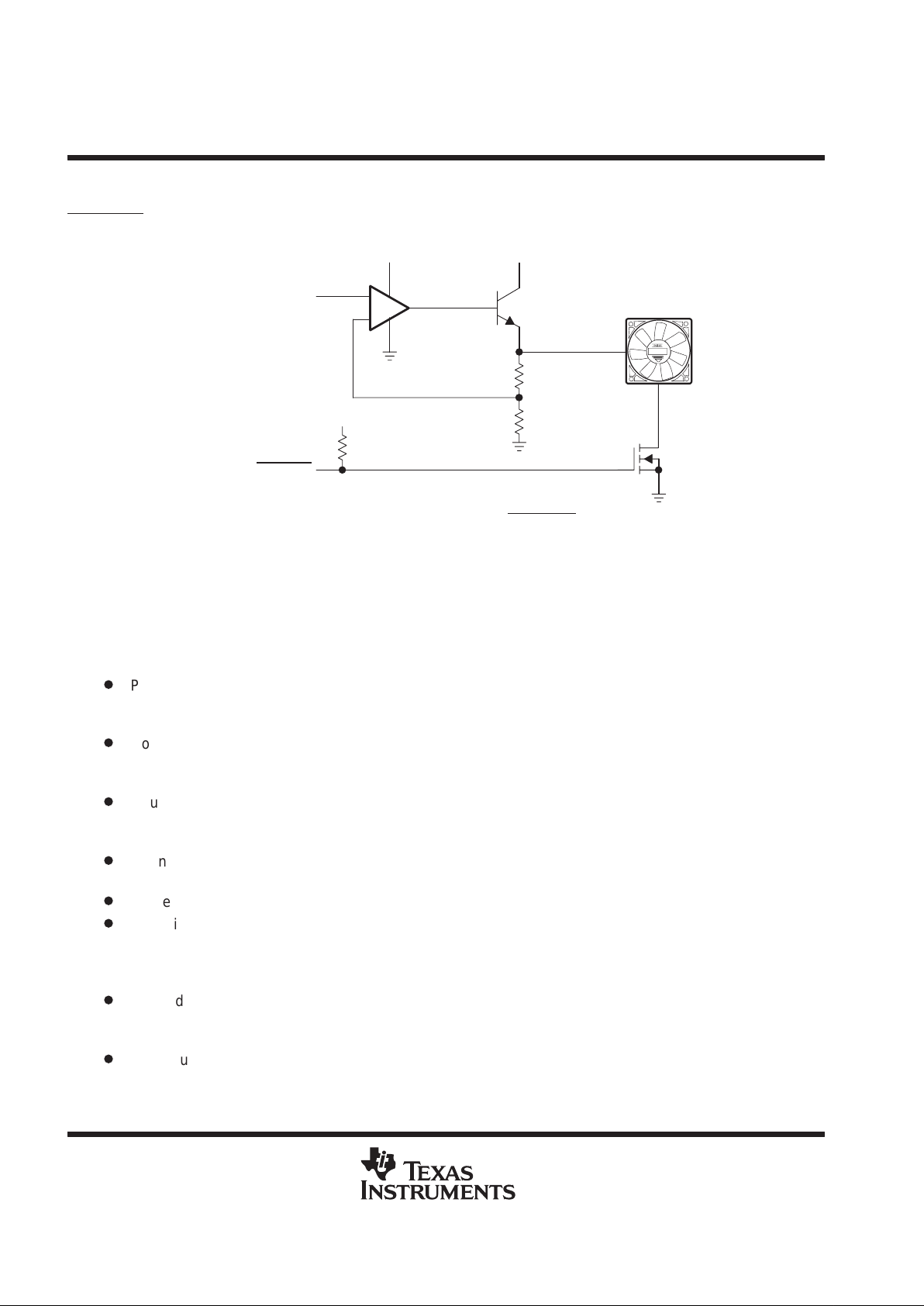
+12 V +12 V
FAN_SPD/NTEST_IN
LM324
Q1
2N2219A
R1
36 kΩ
R2
10 kΩ
_
+
Figure 6. External Fan Drive Circuit Using 1/4 LM324 and NPN Emitter-Follower, Single Supply
+12 V +12 V
FAN_SPD/NTEST_IN
LM324
R4
1 kΩ
R3
1 kΩ
R1
39 kΩ
R2
10 kΩ
Q1
BD136
2SA968
+
–
Figure 7. External Fan Drive Circuit Using 1/4 LM324 and PNP Transistor, Single Supply

THMC50
REMOTE/LOCAL TEMPERATURE MONITOR AND
FAN CONTROLLER WITH SMBus INTERFACE
SLIS090 – JUL Y 1999
13
POST OFFICE BOX 655303 • DALLAS, TEXAS 75265
+12 V
FAN_SPD/NTEST_IN
LM324
R1
39 kΩ
R2
10 kΩ
R3
100 kΩ
Q1
IRF9620
+12 V
+
–
Figure 8. External Fan Drive Circuit Using 1/4 LM324 and P-Channel FET, Single Supply

THMC50
REMOTE/LOCAL TEMPERATURE MONITOR AND
FAN CONTROLLER WITH SMBus INTERFACE
SLIS090 – JUL Y 1999
14
POST OFFICE BOX 655303 • DALLAS, TEXAS 75265
PRINCIPLES OF OPERATION
analog output - FAN_SPD (continued)
FAN_SPD/NTEST_IN
+12 V
R1
100 kΩ
R2
100 kΩ
Q1/Q2
MBT3904
DUAL
Q3
IRF9620
R3
3.9 kΩ
R4
1 kΩ
R5
5 kΩ
Figure 9. External Fan Drive Circuit Using Discrete Components With P-Channel FET, Single Supply
+12 V
FAN_SPD/NTEST_IN
–12 V
R2
100 kΩ
Q1/Q2
MBT3904
DUAL
R1
4.7 kΩ
Q3
IRF9620
R3
39 kΩ
R4
10 kΩ
Figure 10. External Fan Drive Circuit Using Discrete Components With P-Channel FET, Dual Supply
+12 V
FAN_SPD/NTEST_IN
R1
100 kΩ
R2
100 kΩ
Q3
BC556
2N3906
R5
100 Ω
Q1/Q2
MBT3904
DUAL
Q4
BD132
TIP32A
R3
3.9 kΩ
R4
1 kΩ
R6
5 kΩ
Figure 11. External Fan Drive Circuit Using Discrete Components and
PNP Output Transistor, Single Supply

THMC50
REMOTE/LOCAL TEMPERATURE MONITOR AND
FAN CONTROLLER WITH SMBus INTERFACE
SLIS090 – JUL Y 1999
15
POST OFFICE BOX 655303 • DALLAS, TEXAS 75265
PRINCIPLES OF OPERATION
analog output - FAN_SPD (continued)
NOTE:
R5 in Figure 9 and R6 in Figure 11 are required to insure FAN_SPD/NTEST_IN is below the
NTEST_IN enable threshold during power up. Without these pulldown resistors, the external fan
drive circuit would cause the THMC50 to always power up in the NAND tree test mode. If an external
fan drive circuit other than the ones shown above is used, insure that the FAN_SPD/NTEST_IN
terminal is held below 0.3 × VCC3AUX during power up to prevent the THMC50 from entering the
NAND tree test mode inadvertently.
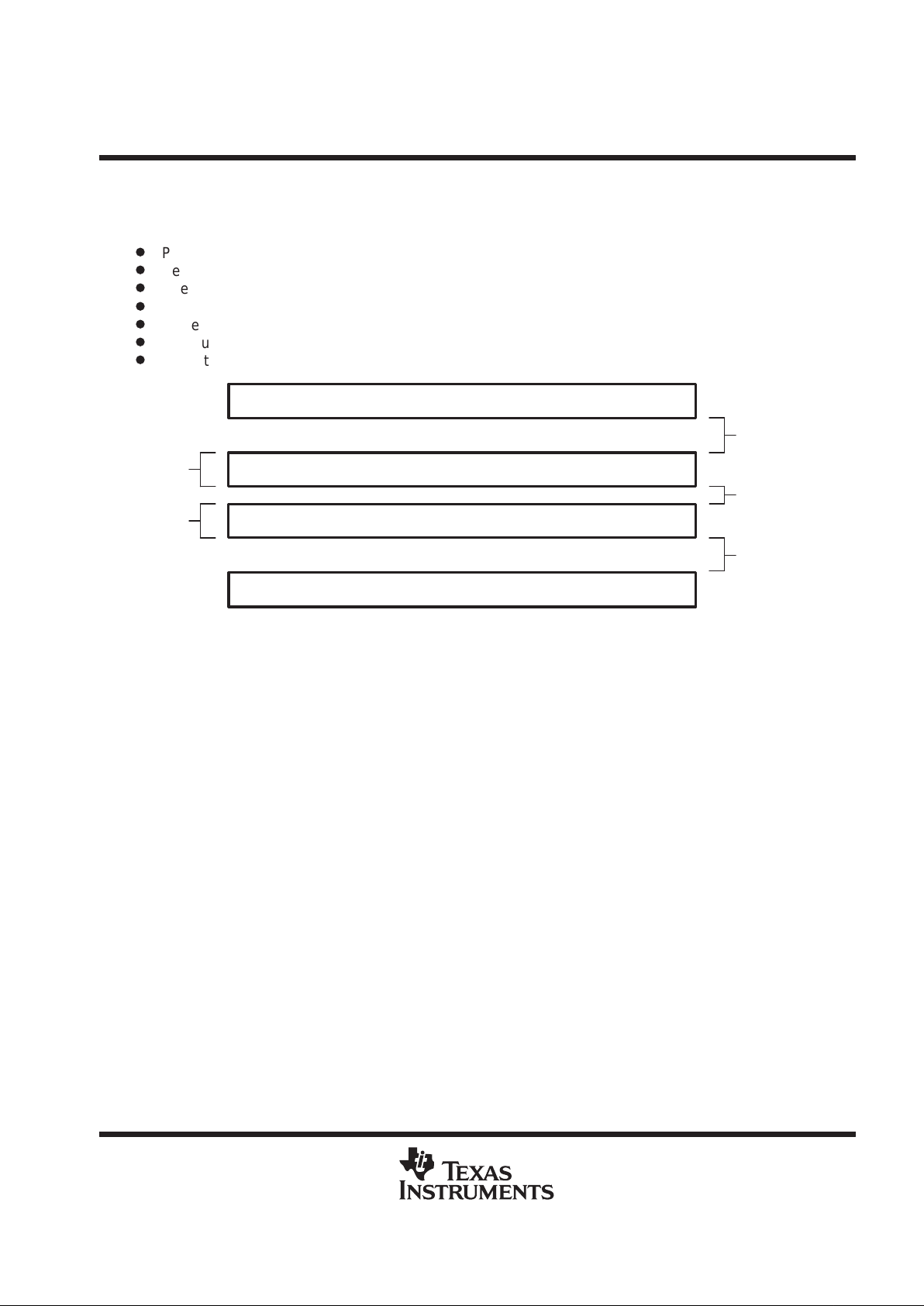
The circuits shown in Figure 6 through Figure 11 should be implemented with the following considerations:
D
The output transistor or FET used must be capable of sourcing a current greater than the maximum fan
current value, and it must be capable of handling the power dissipation generated by the voltage drop across
the device when the fan operates at less than full speed.
D
It may be necessary to add clamping diodes to protect the output transistor or FET from voltage transients
caused by a sudden drop in fan speed from full scale to 0 V.
D
All of the circuits shown in Figure 6 through Figure 1 1 deliver an output voltage swing from near 0 V to near
12 V. The exception is the circuit in Figure 6, which is only able to supply a voltage up to a V
BE
drop down
from 12 V due to the emitter-follower drive stage.
D
If a different circuit is implemented, the gain of the amplifier should be around 4.8 to amplify the F AN_SPD
output from 0 V-to-2.5 V to 0 V-to-12 V.
D
When selecting an operational amplifier, insure that its input common mode range accounts for the range
of the FAN_SPD output (0 V to 2.5 V) and that the output voltage swing of the operational amplifier is
suitable.
D
The operational amplifier can either be powered from 12 V alone or from a ±12 V dual supply. If the
operational amplifier is powered from 12 V only, then the input common mode range of the operational
amplifier should include ground to accommodate the FAN_SPD output voltage range (0 V to 2.5 V). The
output voltage swing of the operational amplifier should be less than 0.6 V, if it is desired to have the fan
turn off when the DAC is commanded to 0x00.
D
Insure that the FAN_SPD/NTEST_IN terminal is held below 0.3 × VCC3AUX during power up to prevent
the THMC50 from entering the NAND tree test mode inadvertently . A pulldown resistor, such as R5 in Figure
9 and R6 in Figure 1 1, may be needed for external circuits to source current into the F AN_SPD/NTEST_IN
terminal to satisfy this requirement.
D
Care should also be taken when using a dual supply for the operational amplifier. Clamping diodes from
the output of the operational amplifier to ground should be used to prevent the base-emitter junction of the
external transistor from being reversed bias if the output of the operational amplifier swings below ground.
FAN_OFF output
The open drain FAN_OFF output of the THMC50 provides a way to turn off the cooling fan regardless of the
voltage on the FAN_SPD analog output terminal. Setting bit 5 in the configuration register (0x40) to a 1 causes
this output to float. Setting bit 5 in the configuration register (0x40) to a 0 causes the output to sink current (go
low). This output can be used in conjunction with an external FET or transistor to gate the fan on or off as shown
in Figure 12.
THMC50
REMOTE/LOCAL TEMPERATURE MONITOR AND
FAN CONTROLLER WITH SMBus INTERFACE
SLIS090 – JUL Y 1999
16
POST OFFICE BOX 655303 • DALLAS, TEXAS 75265
PRINCIPLES OF OPERATION
FAN_OFF
output (continued)
FAN_SPD/NTEST_IN
FAN_OFF
Q1
2N2219A
+12 V+12 V
M1
MMFT3055EL
+5 V
R3
1 kΩ
R1
36 kΩ
R2
10 kΩ
LM324
_
+
Figure 12. Example for Implementing the FAN_OFF Output Signal
layout and grounding
The power supply bypass, the parallel combination of 10 µF (electrolytic or tantalum), and 0.1 µF (ceramic)
bypass capacitors connected between terminals 5, 7, and ground should also be located as close as possible
to the THMC50.
The following are general guidelines for generating the PCB layout for the THMC50:
D
Place the THMC50 as close as practical to the remote diode. In a noisy environment, such as a computer
motherboard, this distance can be 4 inches to 8 inches (typical) or more, as long as the worst noise sources
(such as CRTs, clock generators, memory buses, and ISA/PCI buses) are avoided.
D
Do not route the remote diode lines next to the deflection coils of a CRT . Also, do not route the traces across
a fast memory bus, which can easily introduce 30°C error even with good filtering. Otherwise, most noise
sources are fairly benign.
D
Route the remote diode traces in parallel and in close proximity to each other, away from any high-voltage
traces such as 12 Vdc. Leakage currents from PC board contamination must be taken into consideration,
since a 20 MΩ leakage path from REMOTE_DIODE+ to ground causes about 1°C error.
D
Connect guard traces to GND on either side of the remote diode traces (Figure 13). With guard traces in
place, routing near high-voltage traces is not an issue.
D
Route through as few vias and crossunders as possible to minimize copper/solder thermocouple effects.
D
When introducing a thermocouple, insure that both remote diode traces have matching thermocouples. In
general, PC board induced thermocouples are not a serious problem. A copper-solder thermocouple
exhibits 3 µV/°C, and it takes about 200 µV of voltage error at the remote diode terminals to cause a 1°C
measurement error. Hence, most parasitic thermocouple errors are swamped out.
D
Use wide traces, as narrow ones are more inductive and tend to pick up radiated noise. The 10-mil widths
and spacings recommended in Figure 13 are not absolutely necessary (as they offer only a minor
improvement in leakage and noise), but usage is recommended where practical.
D
Do not use copper as an EMI shield as only ferrous materials such as steel work well. Placing a copper
ground plane between the remote diode traces and traces carrying high-frequency noise signals does not
minimize EMI.
THMC50
REMOTE/LOCAL TEMPERATURE MONITOR AND
FAN CONTROLLER WITH SMBus INTERFACE
SLIS090 – JUL Y 1999
17
POST OFFICE BOX 655303 • DALLAS, TEXAS 75265
PRINCIPLES OF OPERATION
PCB layout checklist
D
Place the THMC50 as close as possible to the remote diode.
D
Keep the remote diode traces away from high voltages (12-V bus).
D
Keep the remote diode traces away from fast data/memory buses and CRTs.
D
Use recommended trace widths and spacings.
D
Place a ground plane under the traces.
D
Use guard traces flanking the remote diode traces and connect them to ground.
D
Place the 0.1-µF VCC3AUX bypass capacitor as close to the THMC50 as possible.
10 MILS
REMOTE_DIODE–
REMOTE_DIODE+
GND
GND
10 MILS
MINIMUM
10 MILS
10 MILS
Figure 13. Recommended PC Board Layout for Remote Diode Traces
use of twisted pair and shielded cables for remote thermal sensor
For remote-sensor distances longer than 8 inches or in particularly noisy environments, a twisted pair is
recommended. Its practical length is 6 feet to 12 feet (typical) before noise becomes a problem, as tested in
a noisy electronics laboratory. For longer distances, the best solution is a shielded twisted pair like that used
for audio microphones. For example, Belden
#8451 works well for distances up to 100 feet in a noisy
environment. Connect the twisted pair to the remote diode terminals and the shield to ground, and leave the
shield’s remote end unterminated. Excess capacitance at REMOTE_DIODE– limits practical remote sensor
distances. For very long cable runs, the cable’s parasitic capacitance often provides noise filtering; hence, the
2200-pF capacitor can often be removed or reduced in value. Cable resistance also affects remote-sensor
accuracy. A 1-Ω series resistance introduces about 0.5°C error.
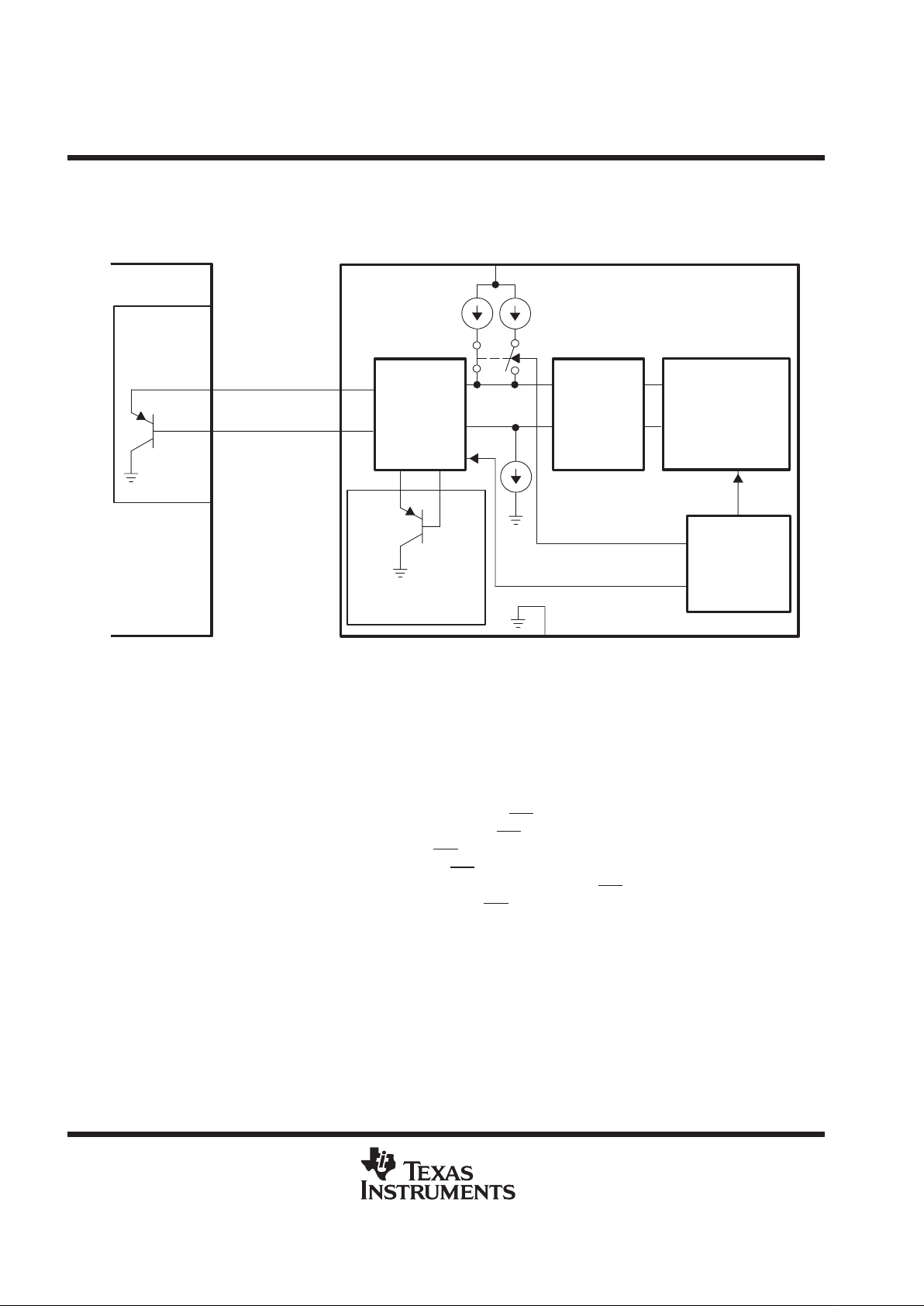
temperature measurement system
The remote thermal diode sensor monitors a remotely placed diode such as those found in some
microprocessors. A 2N3904 transistor can also be used for remote thermal sensing. The THMC50 also has an
internal thermal diode sensor which can be used to monitor the ambient temperature of the environment around
the device. Figure 14 shows the block diagram of the analog front end for the THMC50 temperature-to-digital
converter.
A digital 8-bit comparator is used to compare the temperature readings to the user-programmable high/low, to
over-temperature limit values, and to generate interrupts accordingly.
Belden is a registered trademark of Belden Corporation.
THMC50
REMOTE/LOCAL TEMPERATURE MONITOR AND
FAN CONTROLLER WITH SMBus INTERFACE
SLIS090 – JUL Y 1999
18
POST OFFICE BOX 655303 • DALLAS, TEXAS 75265
PRINCIPLES OF OPERATION
temperature measurement system (continued)
8-Bit A/D
Converter
REMOTE_DIODE+
Substrate
On-Chip Temperature
Sensor
GND
10 µA 90 µA
Control
State
Machine
Analog
MUX
Die
Substrate
REMOTE_DIODE–
Low-Pass
Filter
Remote
Temperature
Sensor
(CPU)
THMC50
Front End
Remote
VCC3AUX
Figure 14. THMC50 Temperature-to-Digital Converter Analog Front-End Block Diagram
temperature interrupts
There are two value RAM limits for the temperature reading that affect the interrupt behavior of the THMC50.
They are remote thermal diode high limit and remote thermal diode low limit.
temperature interrupt operation
Exceeding any of the value RAM thermal limits results in the INT
output being asserted (if the corresponding
mask bits are not set) and respective status bit to be set. The INT
output remains asserted until cleared by either
reading the interrupt status register, or setting the INT
clear (bit 2) of the configuration register. Status bits are
cleared by reading the interrupt status register. The INT
output can only be asserted again if the appropriate
high limit is reprogrammed. If the high limit is not reprogrammed, then the INT
output is asserted again once
the temperature falls below the appropriate low limit. The INT
output is now asserted again if the temperature
again rises above the appropriate high limit or falls below the appropriate low limit. See Figure 15 for an example.

THMC50
REMOTE/LOCAL TEMPERATURE MONITOR AND
FAN CONTROLLER WITH SMBus INTERFACE
SLIS090 – JUL Y 1999
19
POST OFFICE BOX 655303 • DALLAS, TEXAS 75265
PRINCIPLES OF OPERATION
temperature interrupt operation (continued)
100°C
High
Low
Temp
ACPI control
methods clear
event
ACPI control
methods clear
event
ACPI control
methods clear
event
†
†
†
†
†
†
90°C
80°C
70°C
60°C
50°C
40°C
†
ACPI control methods adjust temperature limit values.
INT
Figure 15. Examples of Temperature Interrupt Events
THERM operation
The THERM output is used for fault tolerant fan control. It is asserted by the THMC50 whenever the remote
thermal diode temperature or ambient temperature exceeds the appropriate automatic trip point for three
consecutive acquisitions (see Figure 16). The remote and local thermal diode trip point values are contained
in the programmable remote/local temperature automatic trip point registers (if bit 3 in the configuration register
is set) or the default remote/local temperature automatic trip point (if bit 3 in the configuration register is cleared).
The default trip points are hardware-set trip points that can be read from the value RAM. Programmable trip
points provide for increased flexibility in the ability to tailor the thermal characteristics of the system. The
programmable values can be written to, and then locked down, by writing a 1 to the
write once
bit located in the
configuration register.
THERM
is asserted after three consecutive acquisitions of a remote or an internal temperature that exceeds
the appropriate automatic trip points (based upon bit 3 of the configuration register). When THERM
is asserted
by the THMC50, it remains active (with FAN_SPD = 0xFF and F AN_OFF = FLOATING) until both the local and
remote temperatures fall 5°C below the appropriate automatic trip point values (based upon bit 3 of the
configuration register) for three consecutive temperature acquisitions. Once THERM
has been cleared, the
FAN_SPD output returns to its previously programmed value and FAN_OFF
returns to its previously
programmed state. Note that when FAN_SPD goes to full scale (0xFF) during a THERM
event, the value in the
analog output register (0x19) reflects the previously programmed value and not 0xFF, unless 0xFF was the
previously programmed value. When THERM
is asserted internally, it causes INT to be unconditionally
asserted.
An external device that pulls THERM low causes the fan control to be turned to full on and corresponding status
bits to be set. In addition, whenever THERM
is active, the FAN_OFF bit in the configuration register is
unconditionally set. Note that an INT
generated by an external device pulling THERM low is maskable, but an
INT
generated by an internally generated THERM condition is not maskable.
THMC50
REMOTE/LOCAL TEMPERATURE MONITOR AND
FAN CONTROLLER WITH SMBus INTERFACE
SLIS090 – JUL Y 1999
20
POST OFFICE BOX 655303 • DALLAS, TEXAS 75265
PRINCIPLES OF OPERATION
THERM
operation (continued)
Temperature
5°C
FAN_SPD/NTEST_IN
0xFF
0xFF
Programmed
value
External
THERM
input
THERM
FAN_OFF
FAN_OFF
commanded
low by user
5°C Hysteresis
THERM goes low after three
consecutive readings that exceed
the trip point, and stays low until
three consecutive readings that
are at least 5°C below the trip
point.
Default or
Programmable
THERM
Limit
FAN_SPD/NTEXT_IN goes to full
scale (0xFF) whenever THERM
is
asserted internally or externally,
returns to previously programmed
value once THERM
is cleared.
FAN_OFF floats
high due to THERM
Figure 16. Examples of THMC50 THERM Event Behavior
temperature data format
T emperature data can be read from the remote diode temperature register or the ambient temperature register
in the value RAM (locations 0x26 and 0x27, respectively). Temperature data is represented by an 8-bit, 2s
complement word with an LSB equal to 1°C as shown in Table 2.
Table 2. T
emperature Data Format
DIGITAL OUTPUT
TEMPERATURE
BINARY HEX
125°C 0111 1101 0x7D
25°C 0001 1001 0x19
1°C 0000 0001 0x01
0°C 0000 0000 0x00
–1°C 1111 1111 0xFF
–25°C 1 110 0111 0xE7
–55°C 1100 1001 0xC9
THMC50
REMOTE/LOCAL TEMPERATURE MONITOR AND
FAN CONTROLLER WITH SMBus INTERFACE
SLIS090 – JUL Y 1999
21
POST OFFICE BOX 655303 • DALLAS, TEXAS 75265
PRINCIPLES OF OPERATION
diode fault status
The THMC50 provides for indications of a fault (open or short-circuited) with the remote thermal diode. Before
a remote thermal diode conversion is updated, the status of the remote thermal diode is checked for an
open-circuited or short-circuited condition. If such a fault condition occurs, a status bit is set in the status register,
and an interrupt is generated (unless masked). An open or shorted condition on the remote diode causes the
remote temperature value to read 0x80, does not have an effect on the F AN_SPD output, and does not cause
a THERM
condition.
The following table describes the THMC50 behavior under various remote diode fault conditions:
FAULT CONDITION ON
Remote_Diode+ and Remote_Diode_
REMOTE TEMPERATURE
(REGISTER 0x26)
THERM
ACTIVATED
INT
GENERATED
REMOTE DIODE DEFAULT
STATUS BITS SET
Any remote diode pin open 0x80 No
†
Yes
‡
Yes
Short between Remote_Diode± pins 0x80 No
†
Yes
‡
Yes
Remote_Diode+ short to supply 0x80 No
†
Yes
‡
Yes
Remote_Diode+ short to GND 0x80 No
†
Yes
‡
Yes
Remote_Diode– shorted to supply 0x80 No
†
Yes
‡
Yes
Remote_Diode– shorted to GND Normal operation No
§
No
§
No
†
THERM will not be asserted due to this fault, however, THERM could still activate due to a valid internal temperature THERM condition or if
THERM
is asserted externally.
‡
INT
will not be generated if the Remote diode fault is masked. A remote temperature error INT or a remote temperature error status bit will not
be generated by a faulted remote diode.
§
THERM
or INT will be asserted if the temperature in 0x26 meets the criteria for a THERM or INT event and INT is not masked.
interrupt output
All interrupts are indicated in the interrupt status register and its mirror register. The INT
output has an individual
mask register and individual masks for each interrupt. This hardware interrupt line can also be enabled/disabled
in the configuration register. When enabled, the INT
line reflects all interrupt error conditions. INT can be
generated from the following sources:
D
T emperature Interrupt: An interrupt is generated if a high or a low temperature limit has been exceeded
on either the local or remote thermal diode.
D
Remote Diode Fault Interrupt: An interrupt is generated if either a short-circuit or open-circuit fault exists
on the remote thermal diode inputs.
general-purpose input - GPI
The GPI logic input terminal allows the THMC50 SMBus host to read the logic state of this input terminal by
reading bit 4 of the interrupt status register (0x41). The logic state of the GPI terminal reported in bit 4 of the
interrupt status register (0x41) is inverted from the actual GPI logic state if bit 6 of the configuration register
(0x40) is set to a 1. If bit 6 of the configuration register (0x40) is set to a 0, then bit 4 of the interrupt status register
(0x41) reports the same logic state present on the GPI terminal. The GPI interrupt bit can be masked by setting
bit 4 of the interrupt mask register (0x43) to 1. Note that the state of GPI is not latched into bit 4; this bit simply
reflects the state or inverted state of the GPI terminal. If this bit is 1, reading this register does not clear it to 0.
interrupt clearing
Reading the interrupt status register or the interrupt status register mirror outputs the contents of the register
and resets that register only . A subsequent read done before the next conversion is complete indicates a cleared
register. Allow at least 1.5 seconds for all registers to be updated between reads. In summary, the interrupt
status register clears upon being read, and requires at least 1.5 seconds to be updated. When the interrupt
status register clears, the INT
output also clears until the registers are updated by the next conversion.
THMC50
REMOTE/LOCAL TEMPERATURE MONITOR AND
FAN CONTROLLER WITH SMBus INTERFACE
SLIS090 – JUL Y 1999
22
POST OFFICE BOX 655303 • DALLAS, TEXAS 75265
PRINCIPLES OF OPERATION
interrupt clearing (continued)
The INT output can be cleared with the INT clear bit (bit 2 of the configuration register) without affecting the
contents of the interrupt status register.
reset generators
The THMC50 contains the equivalent of two MAX81 1 microprocessor voltage monitors for generation of system
resets. One of these functions monitors the THMC50 VCC3 terminal connected to the system’s 3.3-V main
power supply. The other function monitors the VCC3AUX terminal connected to the system’s 3.3-V auxiliary
power supply. Each function has a corresponding reset output (RST
, AUXRST) that is used by the core logic
for proper system hardware initialization.
When a particular power supply voltage falls below a threshold of 2.93V (max), the associated reset output is
asserted low for at least 140 ms after the power supply voltage has risen above the threshold (see Figure 18
and Figure 20). The reset outputs are a logic 0 for V
CC
(VCC3 or VCC3AUX) > 1 V.
The THMC50 includes a manual reset input, MR
. When asserted low (0), the RST output is asserted low. This
output remains asserted as long as the MR
input is asserted. Once MR is negated, this reset output continues
to be asserted for 180 ms (typical) (see Figure 17). The MR
input may be used by test equipment or external
logic (e.g., front bezel panel reset button) to initiate a reset independent of power supply voltage status. It is
recommended that a 0.1-µF capacitor be connected between MR
and ground if the terminal is connected to a
long lead/cable length.
Asserting the AUXRST
output causes the RST output to also be asserted regardless of the voltage level on the
VCC3 terminal. This insures that the auxiliary reset output (AUXRST
) is negated before the RST output is
negated. Once AUXRST
is negated, the RST output continues to remain asserted for 180 ms (typical) (see
Figure 19).
The AUXRST
terminal is bidirectional. It can be driven by an external device to force the THMC50 into a hard
reset condition. Insure that other devices connected to AUXRST
are not also reset, if that is an undesirable
behavior. If AUXRST
is only used as an output, then isolation is not necessary.
reset generators timing diagrams
Figure 17 through Figure 20 illustrate the timing relationship of the THMC50 reset generators.
D
Figure 17 shows RST output behavior when the MR input is asserted low.
D
Figure 18 shows RST output behavior according to the voltage seen at the VCC3 terminal.
D
Figure 19 shows RST output behavior whenever an AUXRST is generated or is asserted manually.
D
Figure 20 shows AUXRST output and RST output behavior according to the voltage seen at the VCC3AUX
terminal.
Figure 17. MR
to RST Timing
Figure 18. VCC3 to RST
Timing
MR
RST
TIME
t
(RP)
t
(MR)
VCC3
RST
2.93V
TIME
t
(RP)
t
(VCC3RST)

THMC50
REMOTE/LOCAL TEMPERATURE MONITOR AND
FAN CONTROLLER WITH SMBus INTERFACE
SLIS090 – JUL Y 1999
23
POST OFFICE BOX 655303 • DALLAS, TEXAS 75265
PRINCIPLES OF OPERATION
reset generators timing diagrams (continued)
Figure 19. AUXRST to RST Timing
Figure 20. VCC3AUX, AUXRST,
and RST Timing
RST
TIME
AUXRST
t
(RP)
t
(RST)
VCC3AUX
AUXRST
2.93V
TIME
RST
t
(RP)
t
(RP)
t
(VCC3AUX1)
t
(VCC3AUX2)
NAND tree tests - FAN_SPD/NTEST_IN and ADD/NTEST_OUT
A NAND tree is provided in the THMC50 for automated test equipment (A TE) board level connectivity testing.
If a logic 1 is applied to the FAN_SPD/NTEST_IN input terminal during initial power up, the device is in the NAND
tree test mode and the ADD/NTEST_OUT terminal becomes the NAND tree output. Power must be removed
from the device in order to return to normal operation. To perform a NAND tree test, MR
, SDA, SCL, and GPI
terminals should be initially driven low, and FAN_SPD/NTEST_IN initially driven high. Starting with MR
and
ending with GPI, each input should be toggled high and left high. This results in ADD/NTEST_OUT reflecting
the following pattern: (1 –> 0 –> 1 –> 0 –> 1) (see Figure 21).
Allow for a typical propagation delay of 500 ns.
GPI
SCL
SDA
MR
ADD/NTEST_OUT
D
Q
AUXRST
FAN_SPD/NTEST_IN
ENABLE
ENABLE
GPI
SCL SDA MR ADD/NTEST_OUT
0 0 0 0 1
0 0 0 1 0
0 0 1 1 1
0 1 1 1 0
1 1 1 1 1
Figure 21. NAND Tree Test Equivalent Circuit

THMC50
REMOTE/LOCAL TEMPERATURE MONITOR AND
FAN CONTROLLER WITH SMBus INTERFACE
SLIS090 – JUL Y 1999
24
POST OFFICE BOX 655303 • DALLAS, TEXAS 75265
PRINCIPLES OF OPERATION
NAND tree tests - FAN_SPD/NTEST_IN and ADD/NTEST_OUT (continued)
NOTE:
To properly implement the NAND tree test on the PCB, no terminals listed in the tree should be
connected directly to power or ground. If it is necessary to permanently connect a terminal to
ground, such as an address terminal, it should be connected to ground through a low value resistor,
such as 3.3 kΩ, to allow the system-level ATE to drive it high. All terminals listed in the NAND tree
which need to be permanently tied high should be pulled up to the supply via a resistor to allow the
ATE to drive the node low during the NAND tree test.
registers and RAM
REGISTERS AND RAM A7 - A0 IN HEX POWER ON VALUE OF REGISTERS: <7:0> IN BINARY
Configuration register 0x40 0010 0101
Interrupt status register 0x41 0000 0000
Interrupt mask register 0x43 0000 0000
Interrupt status register mirror 0x4C 0000 0000
Value RAM 0x13 – 0x3D, 0x43 – 0x4A See value RAM section for complete description
Company ID 0x3E Contains company number
Stepping 0x3F Contains stepping number and device version
register 0x40 configuration register
BIT NAME R/W DESCRIPTION
0 Start Read/write Setting this bit to a 1 enables start-up of the THMC50; clearing this bit to 0 places the THMC50 in
standby mode.
Caution: The INT output is not cleared if this bit was cleared after an interrupt has occurred (see INT
clear bit).
At start-up, temperature monitoring and limit checking functions begin. Note: All limit values should
be programmed into the THMC50 prior to using the standard thermal interrupt mechanism based
upon high and low limits. (power-up default=1)
1 INT enable Read/write Setting this bit to a 1 enables the INT output. 1=enabled 0=disabled (power-up default = 0)
2 INT clear Read/Write This bit clears the INT output when set (1) without affecting the contents of the interrupt status
register. (power-up default = 1)
3 Programmable
automatic trip
point control
register write
once bit
Read/write
once
Setting this bit to a 1 locks in the values set into the programmable remote thermal diode automatic
trip point and programmable ambient temperature automatic trip point (value RAM locations 0x14
and 0x13). Furthermore when this bit is set, the values in the default remote thermal diode
automatic trip point and default ambient temperature automatic trip point (value RAM locations
0x18 and 0x17) no longer have an effect on the THERM
, FAN_SPD, or FAN_OFF outputs. This
register is unable to be written again until AUXRST
is asserted. (power-up default = 0)
4 Soft reset Read/write Setting this bit to a 1 restores power-up default values to the configuration register , interrupt status
register, interrupt status register mirror, and interrupt mask register. This bit automatically clears
itself since the power-on default is zero.
5 FAN_OFF Read/write Setting this bit to a 1 causes the FAN_OFF terminal to be floated. Clearing this bit to 0 causes the
FAN_OFF
terminal to be driven low which requests that the fan be turned off. This bit is
unconditionally set if the THERM
terminal is ever asserted. Reading this bit reflects the state of the
FAN_OFF
output buffer. Due to the open drain nature of this terminal, the value read does not
represent the actual state of the external net connected to it. (power-up default =1)
6 GPI invert Read/write Setting this bit to a 1 inverts the GPI input for the purpose of level detection and interrupt generation.
Clearing this bit to 0 leaves the GPI input unmodified. (power-up default=0)
7 Reserved Read/write Reserved (default = 0)

THMC50
REMOTE/LOCAL TEMPERATURE MONITOR AND
FAN CONTROLLER WITH SMBus INTERFACE
SLIS090 – JUL Y 1999
25
POST OFFICE BOX 655303 • DALLAS, TEXAS 75265
PRINCIPLES OF OPERATION
register 0x41 interrupt status register
power-on default <7:0> = 00h
BIT NAME READ/WRITE DESCRIPTION
0 Ambient temperature error Read only A 1 indicates one of the ambient temperature limits has been exceeded.
1 Reserved Read only Undefined (reserved for remote thermal diode 2 temperature error)
2 Reserved Read only Undefined (reserved for remote thermal diode 2 fault)
3 Reserved Read only Undefined
4 GPI input Read only A 1 indicates that the GPI terminal is asserted. The polarity of the GPI terminal is
determined by GPI invert (bit 6) in the configuration register. For example, if GPI invert is
cleared, then this bit is 1 when the GPI terminal is high (1); this bit is 0 when the GPI
terminal is low (0). If GPI invert is set, then this bit is 1 when the GPI terminal is low (0); this
bit is 0 when the GPI terminal is high (1). Note: The state of GPI is not latched; this bit
simply reflects the state or inverted state of the GPI terminal. If this bit is 1, reading this
register does not clear it to 0.
5 Remote temperature error Read only A 1 indicates one of the remote thermal diode limits has been exceeded.
6 THERM input Read only A 1 indicates that the thermal overload (THERM) line has been asserted externally.
7 Remote diode fault Read only A 1 indicates either a short or open circuited fault on the remote thermal diode inputs.
NOTE: An error that causes continuous interrupts to be generated may be masked in its respective mask register, until the error can be alleviated.
register 0x43 interrupt mask register
power-on default <7:0> = 00h
BIT NAME READ/WRITE DESCRIPTION
0 Ambient temperature error Read/write A 1 disables the corresponding interrupt status bit for the INT output.
1 Reserved Read only Undefined (reserved for remote thermal diode 2 temperature error)
2 Reserved Read only Undefined (reserved for remote thermal diode 2 fault)
3 Reserved Read only Undefined
4 GPI input Read/write A 1 disables the corresponding interrupt status bit for the INT output.
5 Remote temperature error Read/write A 1 disables the corresponding interrupt status bit for the INT output.
6 THERM input Read/write A 1 disables the corresponding interrupt status bit for the INT output.
7 Remote diode fault Read/write A 1 disables the corresponding interrupt status bit for the INT output.

THMC50
REMOTE/LOCAL TEMPERATURE MONITOR AND
FAN CONTROLLER WITH SMBus INTERFACE
SLIS090 – JUL Y 1999
26
POST OFFICE BOX 655303 • DALLAS, TEXAS 75265
PRINCIPLES OF OPERATION
register 0x4C interrupt status register 1 mirror
power-on default <7:0> = 00h
BIT NAME READ/WRITE DESCRIPTION
0 Ambient temperature error Read only A 1 indicates one of the ambient temperature limits has been exceeded.
1 Reserved Read only Undefined (reserved for remote thermal diode 2 temperature error)
2 Reserved Read only Undefined (reserved for remote thermal diode 2 fault)
3 Reserved Read only Undefined
4 GPI input Read only A 1 indicates that the GPI terminal is asserted. The polarity of the GPI terminal is
determined by GPI invert (bit 6) in the configuration register. For example, if GPI invert is
cleared, then this bit is 1 when the GPI terminal is high (1); this bit is 0 when the GPI
terminal is low (0). If GPI invert is set, then this bit is 1 when the GPI terminal is low (0); this
bit is 0 when the GPI terminal is high (1). Note: The state of GPI is not latched; this bit
simply reflects the state or inverted state of the GPI terminal. If this bit is 1, reading this
register does not clear it to 0.
5 Remote temperature error Read only A 1 indicates one of the remote thermal diode limits has been exceeded.
6 THERM input Read only A 1 indicates that the thermal overload (THERM) line has been asserted externally.
7 Remote diode fault Read only A 1 indicates either a short or open circuited fault on the remote thermal diode inputs.
register 0x13 - 0x4A value RAM
power-on default are undefined unless stated otherwise
ADDRESS READ/WRITE DESCRIPTION
0x13 Read/write Programmable ambient temperature automatic trip point ≥ default 70°C. This register can only be written if the
write-once bit in the configuration register (0x40, bit 3) has not been set.
0x14 Read/write Programmable remote thermal diode automatic trip point ≥ default 100°C. This register can only be written if the
write-once bit in the configuration register (0x40, bit 3) has not been set.
0x15 Read/write Manufacturer’s test register
0x17 Read only Default ambient temperature automatic trip point ≥ 70° C
0x18 Read only Default remote thermal diode automatic trip point ≥ 100°C
0x19 Read/write Analog output (defaults to 0x00)
0x20 N/A Reserved (for future second remote thermal diode temperature)
0x26 Read only Remote thermal diode temperature
0x27 Read only Ambient temperature
0x2B N/A Reserved (for future second remote thermal diode high limit)
0x2C N/A Reserved (for future second remote thermal diode low limit)
0x37 Read/write Remote thermal diode high limit
0x38 Read/write Remote thermal diode low limit
0x39 Read/write Ambient temperature high limit
0x3A Read/write Ambient temperature low limit
0x3E Read only Company ID number (0x49)
0x3F Read only Stepping ID number and THMC50 version number
0x44 Read/write For manufacturer’s test use (reads or writes have unpredictable results)
0x47 Read/write For manufacturer’s test use (reads or writes have unpredictable results)
0x4A Read/write For manufacturer’s test use (reads or writes have unpredictable results)
NOTE: All unspecified locations are considered as reserved and should not be accessed. Unpredictable results may occur.

THMC50
REMOTE/LOCAL TEMPERATURE MONITOR AND
FAN CONTROLLER WITH SMBus INTERFACE
SLIS090 – JUL Y 1999
27
POST OFFICE BOX 655303 • DALLAS, TEXAS 75265
PRINCIPLES OF OPERATION
manufacturer’s test register - address 0x15
This register should only be used by Texas Instruments for testing. Reading or writing to this register during
normal use leads to erroneous events or measurements.
analog output - address 0x19
This register latches an 8-bit value into an R-2R D/A to provide a range of 0 V–2.5 V , accuracy can be ±5% or
more.
company ID - address 0x3E
This location contains the company identification number for TI – 0x49. This register is read only.
stepping - address 0x3F
This location contains the stepping number of the part in the lower four bits of the register [3:0]. The upper four
bits reflect the THMC50 version number [7:4]. The first version is 1 100. The next version of the THMC50 would
be 1 101, etc. For example, if the stepping were A0 and this part is a THMC50-1, then this register would read
1100 0000. This register is read only.

THMC50
REMOTE/LOCAL TEMPERATURE MONITOR AND
FAN CONTROLLER WITH SMBus INTERFACE
SLIS090 – JUL Y 1999
28
POST OFFICE BOX 655303 • DALLAS, TEXAS 75265
TYPICAL CHARACTERISTICS
ESD protection structures (example method to be used as reference only)
To Internal Circuitry
D1
D2
D3
Analog/Digital Inputs
V+
GND
NOTE:
Diodes are forward biased when the forward voltage exceeds 50 mV.
TERMINAL NAME D1 D2 D3
FAN_OFF X X
MR X X
AUXRST X X
VCC3 X
RST X X
FAN_SPD/NTEST_IN X
SDA X X
SCL X
INT X X X
ADD/NTEST_OUT X X X
GPI X
THERM X X
REMOTE_DIODE+ X
REMOTE_DIODE– X
X - Diode exists

THMC50
REMOTE/LOCAL TEMPERATURE MONITOR AND
FAN CONTROLLER WITH SMBus INTERFACE
SLIS090 – JUL Y 1999
29
POST OFFICE BOX 655303 • DALLAS, TEXAS 75265
TYPICAL CHARACTERISTICS
Ambient
Temperature Error
GPI Input
Remote
Temperature Error
Remote Diode
Fault
INT
Enable
INT
Clear
THERM
INT
THERM Error
6
Ambient
Temperature Error
GPI Input
Remote
Temperature Error
Remote Diode
Fault
THERM
Error
THERM Input
THERM
6
Soft Reset
Soft Reset
Soft Reset
FAN_OFF
GPI Invert
GPI Invert
GPI Invert
0x41
Interrupt
Status
Register
0
4
5
6
7
Cleared on Power Up
After Register is
Read
or Soft Reset = 1
0x4C
Interrupt
Status
Register 1
Mirror
0
4
5
6
7
Cleared on Power Up
After Register is
Read
or Soft Reset = 1
0
4
5
6
7
0
4
5
6
7
0x43
Interrupt
Mask
Register
Cleared on Power Up
or Soft Reset = 1
Status Bit
Mask Bit
0x40
Configuration
12
4
5
6
on Power Up
or Soft Reset = 1
THERM Error
THERM
(Non-Maskable)
Register
Reset to Default Values
66
Figure 22. Interrupt Structure

THMC50
REMOTE/LOCAL TEMPERATURE MONITOR AND
FAN CONTROLLER WITH SMBus INTERFACE
SLIS090 – JUL Y 1999
30
POST OFFICE BOX 655303 • DALLAS, TEXAS 75265
TYPICAL CHARACTERISTICS
Embedded
Controller
With
SMBus
THMC50
VCC3AUX
VCC3AUX
C1
C2
R6
VCC3AUX
AUXRST
VCC3 R7
RST
MR
GPI
R8
THERM
VCC3AUX
R9
INT
VCC3AUX
R10
SCL
VCC3AUX R11
SDA
ADD/NTEST_OUT
VCC3AUX
GND
13 4
9
10
16
15
14
11
12
2
7
3
56
8
1
FAN_OFF
FAN_SPD/NTEST_IN
VCC3
C3
C4
+12V +12V
LM324
+5 V
R3
Q1
2N2219A
R1
R2
MMFT3055EL
M1
REMOTE_DIODE+
REMOTE_DIODE–
B14
B15
C5
2200 pF
R4 R5
VCC3
Pentium
Intel
10 kΩ
10 kΩ
0.1 µF
10 µF
0.1 µF
10 µF
10 kΩ
10 kΩ
36 kΩ
10 kΩ
10 kΩ
10 kΩ
10 kΩ
300 kΩ
10 kΩ
_
+
Figure 23. Typical Application Schematic

THMC50
REMOTE/LOCAL TEMPERATURE MONITOR AND
FAN CONTROLLER WITH SMBus INTERFACE
SLIS090 – JUL Y 1999
31
POST OFFICE BOX 655303 • DALLAS, TEXAS 75265
MECHANICAL DATA
DBQ (R-PDSO-G**) PLASTIC SMALL-OUTLINE PACKAGE
Gage Plane
0.008 (0,20) NOM
0.010 (0,25)
0.016 (0,40)
0.035 (0,89)
2420
Seating Plane
(8,74)
(8,56)
0.3370.337
(8,56)
(8,74)
0.344 0.344
4073301/D 08/98
13
0.150 (3,81)
0.157 (3,99)
0.012 (0,30)
0.008 (0,20)
12
A
24–PIN SHOWN
1
24
16
DIM
PINS **
A MIN
A MAX
0.004 (0,10)
0.010 (0,25)
0.069 (1,75) MAX
0.244 (6,20)
0.228 (5,80)
0.197
(5,00)
(4,78)
0.188
0.004 (0,10)
M
0.005 (0,13)
0.025 (0,64)
0°–8°
NOTES: A. All linear dimensions are in inches (millimeters).
B. This drawing is subject to change without notice.
C. Body dimensions do not include mold flash or protrusion not to exceed 0.006 (0,15).
D. Falls within JEDEC MO-137

IMPORTANT NOTICE
T exas Instruments and its subsidiaries (TI) reserve the right to make changes to their products or to discontinue
any product or service without notice, and advise customers to obtain the latest version of relevant information
to verify, before placing orders, that information being relied on is current and complete. All products are sold
subject to the terms and conditions of sale supplied at the time of order acknowledgement, including those
pertaining to warranty, patent infringement, and limitation of liability.
TI warrants performance of its semiconductor products to the specifications applicable at the time of sale in
accordance with TI’s standard warranty. Testing and other quality control techniques are utilized to the extent
TI deems necessary to support this warranty. Specific testing of all parameters of each device is not necessarily
performed, except those mandated by government requirements.
CERT AIN APPLICATIONS USING SEMICONDUCTOR PRODUCTS MAY INVOLVE POTENTIAL RISKS OF
DEATH, PERSONAL INJURY, OR SEVERE PROPERTY OR ENVIRONMENTAL DAMAGE (“CRITICAL
APPLICATIONS”). TI SEMICONDUCTOR PRODUCTS ARE NOT DESIGNED, AUTHORIZED, OR
WARRANTED TO BE SUITABLE FOR USE IN LIFE-SUPPORT DEVICES OR SYSTEMS OR OTHER
CRITICAL APPLICATIONS. INCLUSION OF TI PRODUCTS IN SUCH APPLICA TIONS IS UNDERST OOD TO
BE FULLY AT THE CUSTOMER’S RISK.
In order to minimize risks associated with the customer’s applications, adequate design and operating
safeguards must be provided by the customer to minimize inherent or procedural hazards.
TI assumes no liability for applications assistance or customer product design. TI does not warrant or represent
that any license, either express or implied, is granted under any patent right, copyright, mask work right, or other
intellectual property right of TI covering or relating to any combination, machine, or process in which such
semiconductor products or services might be or are used. TI’s publication of information regarding any third
party’s products or services does not constitute TI’s approval, warranty or endorsement thereof.
Copyright 1999, Texas Instruments Incorporated
 Loading...