THMC40, THMC41
VARIABLE SPEED 12-VDC BRUSHLESS FAN MOTOR DRIVERS
SLIS097 – MARCH 2000
1
POST OFFICE BOX 655303 • DALLAS, TEXAS 75265
D
DC Fan Drive Speed Control With No
External Power Drive Stage Required
D
11% to 100% PWM Range Adjustable Via
0–2.5 V DC Control Voltage – Suited for
Cooling Fan Applications Requiring
Variable RPM to Reduce Noise and/or
Increase MTBF
D
Speed Control Capability With Either DC or
PWM Input Signal for Greater System-Level
Flexibility
D
Sleep-State Mode to Eliminate External Fan
ON/OFF Power Device – Suited for Cooling
Fans
in Instantly Available
PCs
D
Thermal Shutdown Protection
D
High Impedance V
PWM
Input for Speed
Control of Multiple Fans With a Single
Signal
D
Locked Rotor Protection (THMC40,
THMC41) With Open-Drain Output
Indication (THMC41)
D
Open-Drain Tachometer Signal Valid Over
Entire RPM Range (THMC40)
D
Noise Immune Signal Conditioning to Allow
Use of Low-Cost Hall Effect Position
Sensor
D
Patented High Efficiency Drive Topology
With Integrated Low R
DS(ON)
LDMOS
Output Drivers
1
2
3
4
5
6
7
14
13
12
11
10
9
8
C
OSC
TACH
CP
V
PWR
V
OUT
NC
PGND
V
PWM
H+
H–
PHA
PHB
AGND
NC
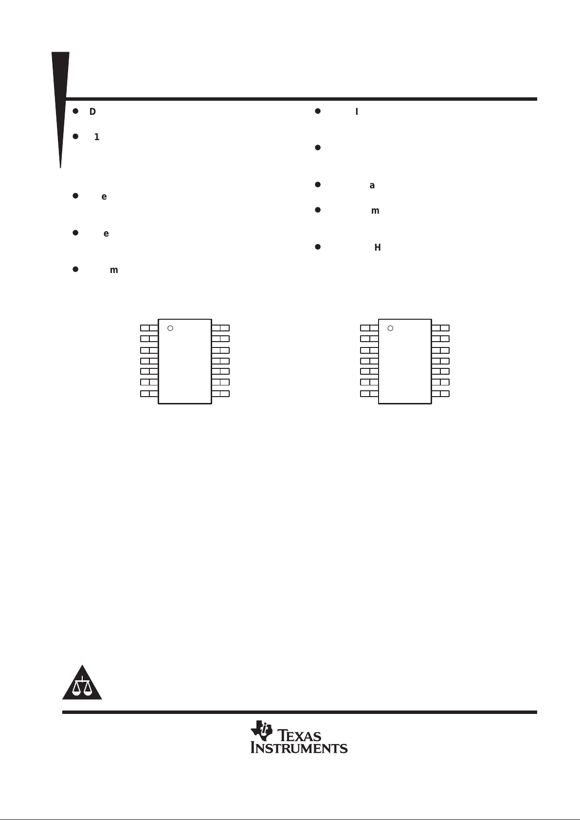
THMC40 ...TACH OUTPUT
14-Pin SOP D Package
(TOP VIEW)
1
2
3
4
5
6
7
14
13
12
11
10
9
8
C
OSC
RD
CP
V
PWR
V
OUT
NC
PGND
V
PWM
H+
H–
PHA
PHB
AGND
NC
THMC41 . . . RD OUTPUT
14-Pin SOP D Package
(TOP VIEW)
description
The THMC40 and THMC41 are 2-phase, dc brushless motor (BLM) drive and control devices intended for use
with 12-Vdc cooling fans. Both devices include a high-efficiency PWM drive topology using integrated 0.5-Ω
(typical) LDMOS drivers, plus a speed control input stage to provide the industry’s first solution for efficient
speed control
inside
dc cooling fans. This patented solution eliminates the need for power drive components
on the main system board, thus reducing printed-circuit board (PCB) component count, PCB space, and
assembly time. This solution also offers other advantages over the two commonly used fan speed control
methods, adjustable external dc supply voltage, and adjustable external PWM drive duty cycle.
Unlike other methods which control speed external to the cooling fan, the THMC40 and THMC41 high-efficiency
PWM drive stage adjusts only the level of motor phase winding power. All other circuitry inside the fan obtains
power from the fixed dc voltage fan supply. This method eliminates the typical problem associated with an
external dc voltage regulation method causing loss of headroom to internal control circuitry at low fan supply
voltage and the resulting limitation of low-speed operation to ≈40%. The PWM drive method employed by the
THMC40 and THMC41 also reduces fan supply power consumption over the external linear regulation method,
which has V×I power loss due to the voltage drop across the regulator.
An external PWM drive method disrupts power to the motor and also to all internal fan circuitry . The THM40 and
THMC41 solution maintains all signal integrity with phase drive commutation and tachometer, while providing
reliable low speed fan operation down to 1 1% PWM. This method allows fan health monitoring over the full fan
speed range.
Copyright 2000, Texas Instruments Incorporated
PRODUCTION DATA information is current as of publication date.
Products conform to specifications per the terms of Texas Instruments
standard warranty. Production processing does not necessarily include
testing of all parameters.
Please be aware that an important notice concerning availability, standard warranty, and use in critical applications of
Texas Instruments semiconductor products and disclaimers thereto appears at the end of this data sheet.
THMC40, THMC41
VARIABLE SPEED 12-VDC BRUSHLESS FAN MOTOR DRIVERS
SLIS097 – MARCH 2000
2
POST OFFICE BOX 655303 • DALLAS, TEXAS 75265
description (continued)
The V
OUT
duty cycle, and thus the motor speed, is proportional to the voltage present at the V
PWM
input terminal.
This terminal allows controlling the fan speed via a DAC output from an external control IC or an RC-filtered
PWM output from a PC Super I/O chip.
The THMC40 and THMC41 have an internal Hall sensor amplifier and signal conditioner, global thermal
shutdown, locked rotor protection, and automatic restart after a locked rotor condition. The THMC40 provides
an open-drain tachometer output signal, while the THMC41 provides an open-drain locked rotor detection
output signal. These devices also provide a sleep-state mode to eliminate the need for an external power
component to disconnect the fan from the supply during a system sleep state or
instantly available
power down.
The THMC40 and THMC41 are primarily intended for cooling fan applications that require RPM speed control
and the availability of a tachometer or locked rotor detection signal.
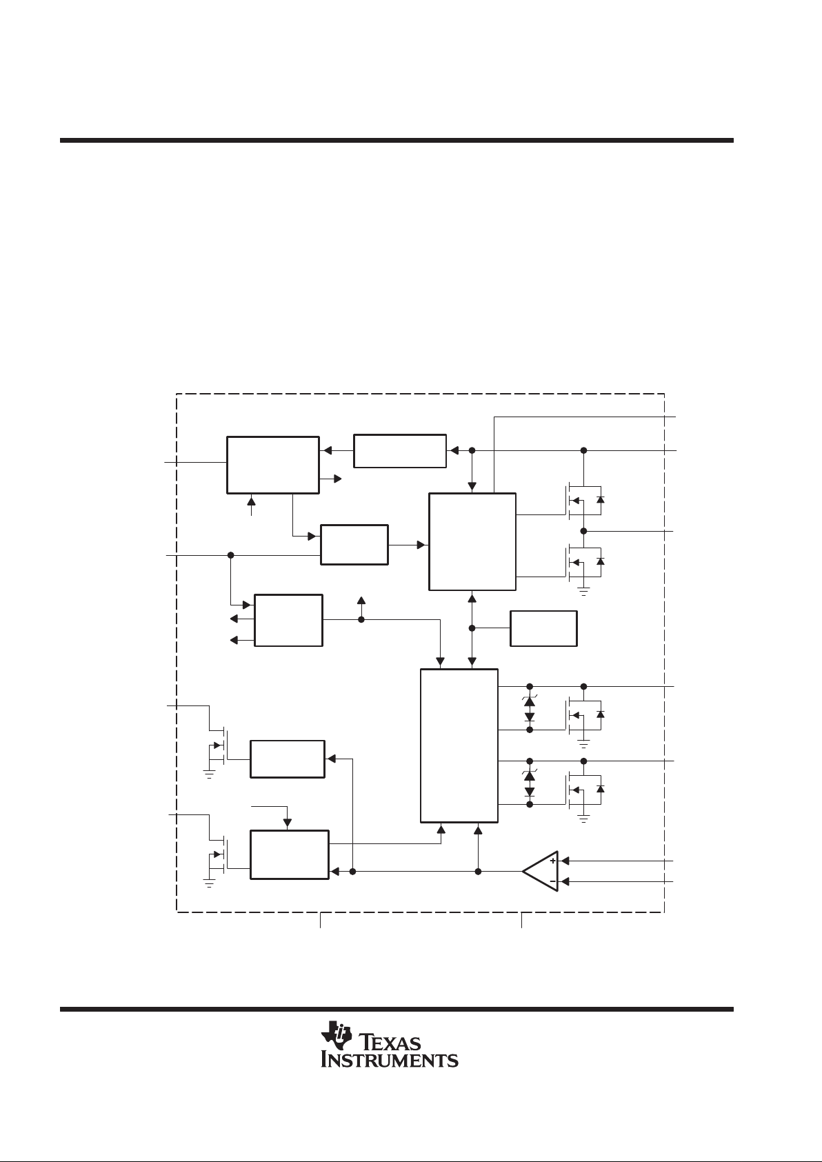
functional block diagram
Tachometer
Output
CP
V
PWM
Low-Side
Gate Drive
Control Logic
and Global
Thermal
Shutdown
High-Side Gate
Drive With
Synchronous
Rectification
Charge Pump
Locked Rotor
Detection and
Auto Restart
SLEEP
START and
SLEEP
Detection
PWM
Generator
PWM
Oscillator
23 kHz Nominal
PUC and V
REF
Thermal
Shutdown
OSC
V
START
V
SLEEP
OSC
PWM
SLEEP
C
OSC
TACH
(THMC40)
RD
(THMC41)
V
PWR
V
OUT
PHA
PHB
H+
H–
PGNDAGND
Hall Sensor
Comparator
THMC40, THMC41
VARIABLE SPEED 12-VDC BRUSHLESS FAN MOTOR DRIVERS
SLIS097 – MARCH 2000
3
POST OFFICE BOX 655303 • DALLAS, TEXAS 75265
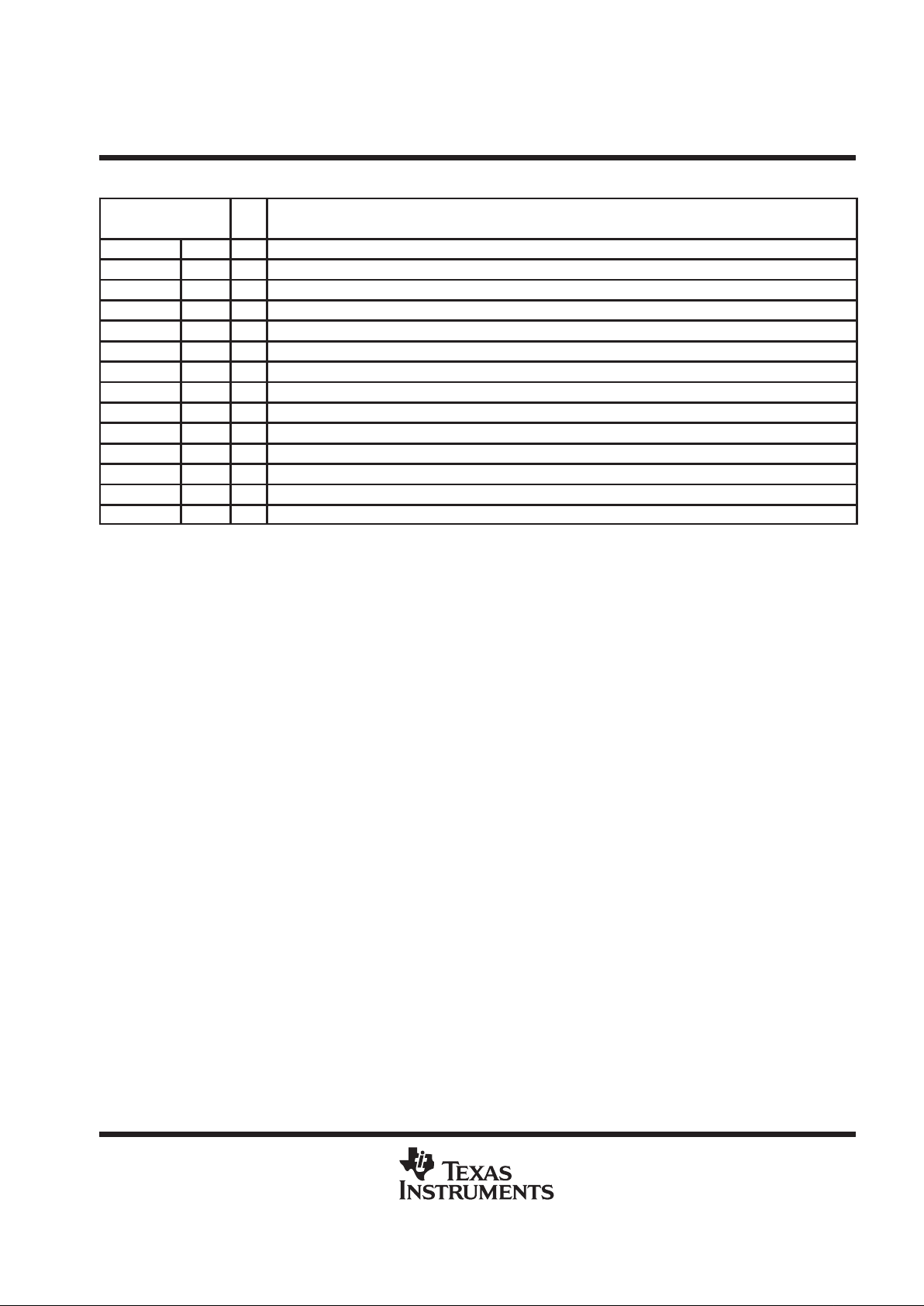
Terminal Functions
TERMINAL
NAME NO.
I/O
DESCRIPTION
AGND 9 I IC analog ground and substrate connection
CP 3 I External charge pump capacitor
C
OSC
1 I/O External oscillator capacitor
H– 12 I Hall sensor negative input
H+ 13 I Hall sensor positive input
NC 6, 8 – No connection
PGND 7 I Power ground for high-side charge pump
PHA 11 O Low-side driver for phase A motor winding
PHB 10 O Low-side driver for phase B motor winding
RD 2 O Open-drain locked rotor detection output—THMC41 only
TACH 2 O Open-drain tachometer output signal—THMC40 only
V
OUT
5 O High-side PWM driver output for motor windings
V
PWR
4 I Supply voltage input
V
PWM
14 I PWM duty cycle control voltage input
absolute maximum ratings over operating case temperature range (unless otherwise noted)
†
(see Note 1)
Supply voltage input, V
PWR
18 V. . . . . . . . . . . . . . . . . . . . . . . . . . . . . . . . . . . . . . . . . . . . . . . . . . . . . . . . . . . . . . . . .
High-side driver, PWM output voltage, V
OUT
18 V. . . . . . . . . . . . . . . . . . . . . . . . . . . . . . . . . . . . . . . . . . . . . . . . . .
Low-side drivers, phase A and B output, V
PHA
, V
PHB
40 V. . . . . . . . . . . . . . . . . . . . . . . . . . . . . . . . . . . . . . . . . .
Hall sensor amplifier input voltage, V
H+
, VH– 7 V. . . . . . . . . . . . . . . . . . . . . . . . . . . . . . . . . . . . . . . . . . . . . . . . . . .
PWM duty cycle control input voltage, V
PWM
7 V. . . . . . . . . . . . . . . . . . . . . . . . . . . . . . . . . . . . . . . . . . . . . . . . . . .
Open-drain tachometer output voltage (THMC40), V
TACH
, or open-drain RD output voltage
(THMC41), VRD 7 V. . . . . . . . . . . . . . . . . . . . . . . . . . . . . . . . . . . . . . . . . . . . . . . . . . . . . . . . . . . . . . . . . . . . . . . . .
Oscillator capacitor voltage, V
COSC
7 V. . . . . . . . . . . . . . . . . . . . . . . . . . . . . . . . . . . . . . . . . . . . . . . . . . . . . . . . . . .
Charge pump capacitor voltage, VCP 30 V. . . . . . . . . . . . . . . . . . . . . . . . . . . . . . . . . . . . . . . . . . . . . . . . . . . . . . . . .
Continuous high-side PWM output source/sink current, I
OUT
1.5 A. . . . . . . . . . . . . . . . . . . . . . . . . . . . . . . . . . .
Continuous low-side PWM output sink current, I
PHA
, I
PHB
1.5 A. . . . . . . . . . . . . . . . . . . . . . . . . . . . . . . . . . . . .
Junction-to-case thermal resistance, R
θJC
26.9°C/W. . . . . . . . . . . . . . . . . . . . . . . . . . . . . . . . . . . . . . . . . . . . . . .
Junction-to-ambient thermal resistance , R
θJA
(see Note 2) 122.3°C/W. . . . . . . . . . . . . . . . . . . . . . . . . . . . . . .
Continuous power dissipation at 25°C , P
D
(see Note 3) 1022 mW. . . . . . . . . . . . . . . . . . . . . . . . . . . . . . . . . . .
Power derating factor above 25°C ambient , P
DERA TING
(see Note 4) 8.18 mW/°C. . . . . . . . . . . . . . . . . . . . .
Operating case temperature range, TC –30°C to 80°C. . . . . . . . . . . . . . . . . . . . . . . . . . . . . . . . . . . . . . . . . . . . . .
Storage temperature range, T
stg
–55°C to 150°C. . . . . . . . . . . . . . . . . . . . . . . . . . . . . . . . . . . . . . . . . . . . . . . . . . .
Maximum junction temperature, T
J
150°C. . . . . . . . . . . . . . . . . . . . . . . . . . . . . . . . . . . . . . . . . . . . . . . . . . . . . . . . .
Lead temperature (soldering, 10 sec), T
LEAD
300°C. . . . . . . . . . . . . . . . . . . . . . . . . . . . . . . . . . . . . . . . . . . . . . . .
†
Stresses beyond those listed under “absolute maximum ratings” may cause permanent damage to the device. These are stress ratings only, and
functional operation of the device at these or any other conditions beyond those indicated under “recommended operating conditions” is not
implied. Exposure to absolute-maximum-rated conditions for extended periods may affect device reliability.
NOTES: 1. All voltage values are with respect to GND.
2. JEDEC low-K board with 0 LFM airflow
3. 150°C maximum junction temperature, JEDEC low-K board with 0 LFM airflow
4. 80°C maximum ambient and 150°C maximum junction temperature
THMC40, THMC41
VARIABLE SPEED 12-VDC BRUSHLESS FAN MOTOR DRIVERS
SLIS097 – MARCH 2000
4
POST OFFICE BOX 655303 • DALLAS, TEXAS 75265
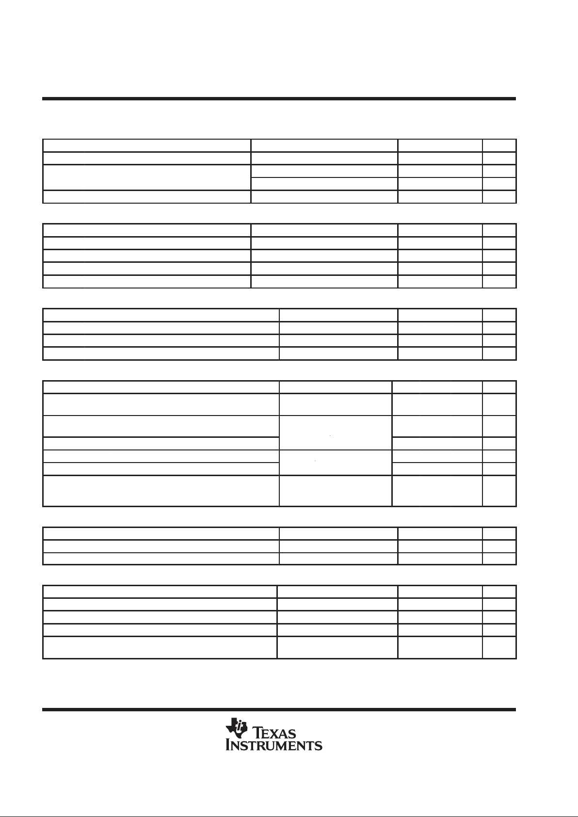
dc electrical characteristics, V
PWR
= 12 V, TA = – 30°C to 80°C (unless otherwise noted)
supply current
PARAMETER TEST CONDITIONS MIN TYP MAX UNITS
V
PWR
Supply voltage range 11 12 13 V
pp
Idle condition in locked rotor detect 2.5 5 mA
I
VPWR
V
PWR
su
pply current
I
LOAD
= –1 A, V
OUT
low, TA = 25°C 5 mA
I
SLEEP
Sleep-state current V
PWM
≤ 0.4 V 300 400 µA
PHA, PHB low-side phase winding driver outputs
PARAMETER TEST CONDITIONS MIN TYP MAX UNITS
I
LEAK
PHA,PHB output leakage current Output = OFF, V
PHx
= 12 V 0.1 10 µA
V
OL
PHA, PHB low-level output voltage Output = ON, I
PHx
= 1 A, TA = 25°C 0.5 0.6 V
R
DS(ON)
PHA, PHB output ON resistance Output = ON, I
PHx
= 1A, TA = 25°C 0.5 0.6 Ω
V
CLAMP
PHA, PHB output active clamp voltage Output = OFF, I
PHx
= 200 mA 32 38 V
Hall sensor signal conditioning
PARAMETER TEST CONDITIONS MIN TYP MAX UNITS
I
IB(HL)
Hall input bias current ±0.1 ±1 µA
V
ICR(HL)
ICR(HL) common-mode input voltage range 1 3.5 V
V
IO
Hall comparator input offset voltage Over V
ICR(HL)
= 1 V to 3.5 V –7 0 7 mV
V
OUT
high-side phase winding driver output
PARAMETER TEST CONDITIONS MIN TYP MAX UNITS
I
LEAK
V
OUT
output sleep-state leakage current
Sleep state engaged,
V
VOUT
= 0 V to V
PWR
±0.1 ±10 µA
V
OH
V
OUT
high-level output voltage
Run state, Output high
I
= –1 A, T
= 25°C
V
PWR
– 0.4
V
PWR
– 0.6
V
R
DS(ON)
V
OUT
output high-side resistance to V
PWR
VOUT
,
A
0.4 0.6 Ω
V
RECIR
V
OUT
output recirculation voltage
Run state, Output low
– 0.3 – 0.5 V
R
DS(ON)(SYNC)VOUT
synchronous switch resistance to PGND
,
I
VOUT
= –1 A, TA = 25°C
0.3 0.5 Ω
I
LIMIT
Pulsed V
OUT
synchronous rectification current
limit
Run state, V
OUT=VPWR
=12V,
V
COSC
> V
PWM,
t
PULSE
= 100 µs, See Note 5
2 2.6 A
CP high-side gate drive charge pump capacitor input
PARAMETER TEST CONDITIONS MIN TYP MAX UNITS
V
CP
Charge pump voltage I
VCP
= –60 µA, V
PWM
= 2.5 V 22 26 V
V
CP(UVLO)VCP
undervoltage lock-out 6.5 7.6 8.5 V
C
OSC
external oscillator capacitor
PARAMETER TEST CONDITIONS MIN TYP MAX UNITS
I
CHARGE
C
OSC
charge source current V
COSC
= 1.4 V, Charge mode –130 –180 –230 µA
I
DISCHARGECOSC
discharge sink current V
COSC
= 1.4 V, Discharge mode 130 180 230 µA
V
DISCHARGECOSC
upper threshold for switching to current sink 2 2.3 2.6 V
V
CHARGE
C
OSC
lower threshold for switching to current
source
0.43 0.5 0.57 V
NOTE 5: V
OUT
current limit, in conjunction with thermal shutdown function, provides device survivability under V
OUT
-to-V
PWR
short condition.
THMC40, THMC41
VARIABLE SPEED 12-VDC BRUSHLESS FAN MOTOR DRIVERS
SLIS097 – MARCH 2000
5
POST OFFICE BOX 655303 • DALLAS, TEXAS 75265
dc electrical characteristics, V
PWR
= 12 V , TA = –30°C to 80°C (unless otherwise noted) (continued)
V
PWM
high-side PWM duty cycle adjust input
PARAMETER TEST CONDITIONS MIN TYP MAX UNITS
I
IB(PWM)
V
PWM
input bias current V
PWM
= 0 V to 3 V ±1 µA
V
PWM
(100%) V
PWM
voltage equivalent to 100% duty cycle 2.3 V
V
SLEEP
V
PWM
voltage threshold to engage sleep mode 0.6 0.7 V
V
START
V
PWM
voltage threshold to disengage sleep
mode
0.8 0.9 V
thermal shutdown characteristics
PARAMETER TEST CONDITIONS MIN TYP MAX UNITS
T
TSD
V
OUT
, PHA, PHB global thermal shutdown
thresholds
Temperature increasing until outputs are off,
See Note 6
150 185 °C
T
HYST
Thermal shutdown hysteresis
After T
TSD
, temperature decreasing until out-
puts return to normal operation, See Note 6
15 °C
TACH Tachometer open-drain output (THMC40)
PARAMETER TEST CONDITIONS MIN TYP MAX UNITS
I
TACHLEAK
TACH high-level output leakage current V
TACH
= 5 V 0.1 1 µA
V
OL
TACH low-level output voltage I
TACH
= 5 mA 0.1 0.3 V
RD locked rotor detection open-drain output (THMC41)
PARAMETER TEST CONDITIONS MIN TYP MAX UNITS
I
RDLEAK
RD high-level output leakage current VRD = 5 V, Locked rotor condition 0.1 1 µA
V
OL
RD low-level output voltage IRD = 5 mA, No locked rotor 0.1 0.3 V
ac electrical characteristics, V
PWR
= 12 V, TA = –30°C to 80°C (unless otherwise noted)
PARAMETER TEST CONDITIONS MIN TYP MAX UNITS
f
PWM
High-side gate drive PWM frequency C
OSC
= 2200 pF 22.7 kHz
t
RD
Locked rotor detect delay time
p
1 s
t
RETRY
Auto-restart delay time
C
OSC
=
2200 pF, See Figure 9
8 s
t
HALL
Hall zero-crossing deglitch time
25 µs
t
DEAD(PHx)
Dead time between phase commutations
See Figure 2
5 µs
t
f(OUT)
V
OUT
output fall time 25 ns
t
r(OUT)
V
OUT
output rise time
R
= 20 Ω , L
= 5 mH,
25 ns
t
f(PHx)
PHA or PHB fall time
L
,
L
,
See Note 6
1 µs
t
r(PHx)
PHA or PHB rise time 1 µs
NOTE 6: Design targets only. Not tested in production.
THMC40, THMC41
VARIABLE SPEED 12-VDC BRUSHLESS FAN MOTOR DRIVERS
SLIS097 – MARCH 2000
6
POST OFFICE BOX 655303 • DALLAS, TEXAS 75265
PRINCIPLES OF OPERATION
general overview
The THMC40 and THMC41 are 2-phase dc brushless fan motor drivers with PWM speed control intended
primarily for applications requiring a wide speed control range and an open-drain tachometer output signal
(THMC40), or a locked rotor detection output (THMC41). The V
OUT
drive duty cycle, and thus fan speed, is
proportional to the voltage level at the V
PWM
input terminal. Each device has an internal Hall sensor
comparator/signal conditioner, a low power sleep-state mode, locked rotor protection with automatic restart
after a locked rotor condition, and over-temperature protection. The tachometer signal (THMC40) can be used
to monitor the
health
of the fan or to close an external loop based on fan RPM. The THMC40 and THMC41
provide a more efficient drive solution to fan RPM control than external linear voltage control. This solution is
also considerably more efficient than controlling dc brushless fan RPM using external PWM drive.
low-side motor phase winding driver outputs (PHA, PHB)
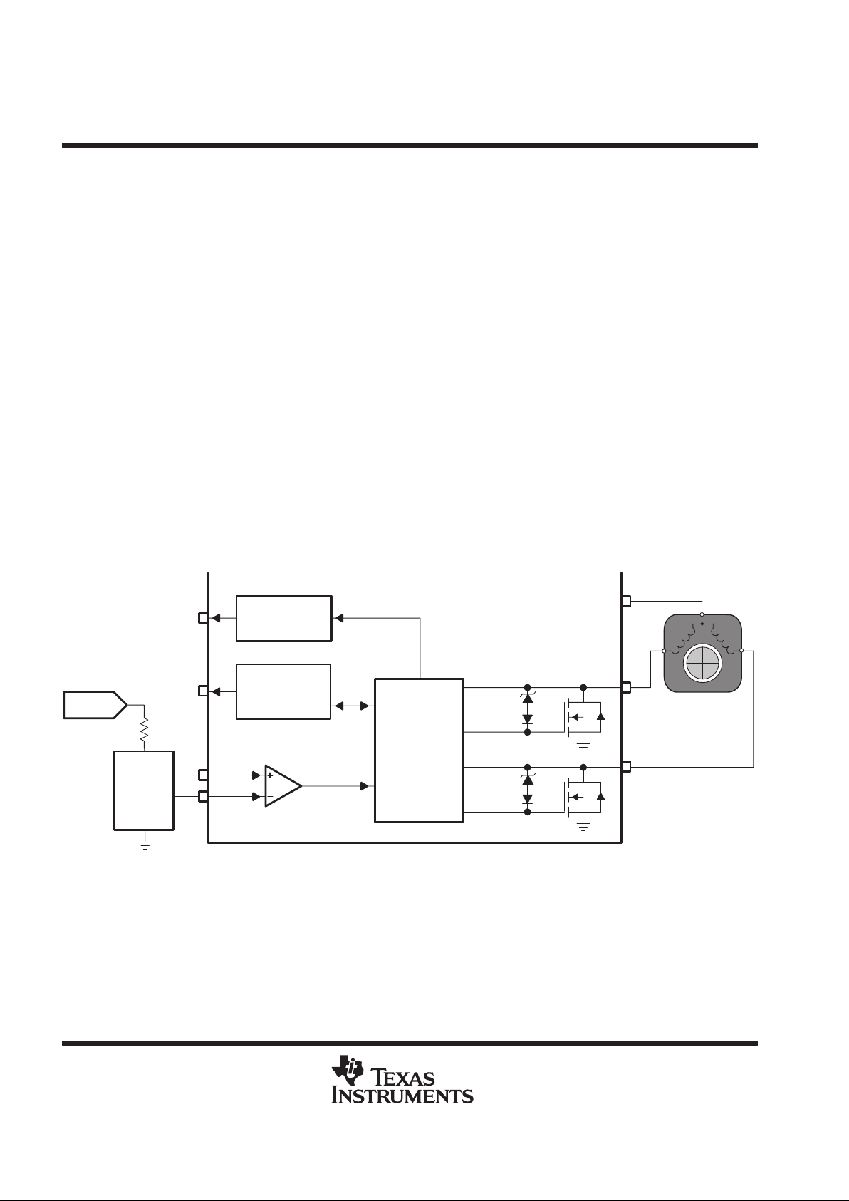
The PHA and PHB outputs provide low-side drive of the motor’s two stator phase windings (see block diagram
and Figure 1). These outputs have a typical R
DS(ON)
of 400 mΩ at 25°C and a 1-A continuous current rating.
The PHA and PHB outputs have an active flyback clamp (V
ZCLAMP
in Figure 1) of 38 V (typical) to snub inductive
energy when a phase drive switches off. The outputs also have global thermal shutdown to prevent device
failure.
Drive commutation of PHA and PHB outputs is controlled according to rotor position monitored by a Hall-effect
position sensor. Discussion of this function is found in the following section, and the relationship between PHA
and PHB outputs to Hall input signal is shown in Figure 2.
Locked Rotor
Detection and
Auto-Restart
V
OUT
TACH
(THMC40)
NS
SN
Tachometer
Output Driver
V
ZCLAMP
V
ZCLAMP
Low-Side
Gate Drive
Control
Logic, and
Global
Thermal
Shutdown
Naked
Hall
Sensor
V
PWR
Hall Sensor
Comparator
RD
(THMC41)
H+
H–
PHA
PHB
Figure 1. Low-Side Gate Drive Block Diagram
 Loading...