

PanelBus DVI RECEIVER WITH TRIPLE DAC
SLDS122A – MARCH 2000 – REVISED JUNE 2000
D
Supports VGA to UXGA Resolutions (Pixel
Rates up to 165 MHz)
D
Digital Visual Interface (DVI) 1.0
Specification Compliant
D
Integrated 165 MHz Triple 8-Bit Video DAC
1
Provides VGA Outputs
D
True-Color, 24 Bits/Pixel, 16.7 M Colors
D
Skew Tolerant Up to One Full Input Clock
Cycle
D
4x Over-Sampling
description
The TFP9431 is a PanelBust digital display product, part of a comprehensive family of end-to-end DVI 1.0
compliant solutions. Targeted at premium digital CRT monitors, the TFP9431 finds applications in designs
requiring a high-speed digital interface with analog output.
The TFP9431 integrates a 165 MHz PanelBust receiver core with a 165 MHz triple 8-bit video DAC to provide
a single chip solution for enabling next generation CRT monitors requiring digital connectivity and enhanced
display quality . The TFP9431 supports display resolutions up to UXGA (1600 x 1200) at 60 Hz and a 24-bit color
depth (16.7 M colors).
D
Laser Trimmed Input Stage for Optimum
Fixed Impedance Matching
D
Reduced Power Consumption - 1.8 V Core
Operation With 3.3 V I/Os and Supplies
D
Lowest Noise and Best Power Dissipation
Using PowerP ADt Packaging
D
Advanced Technology Using Texas
Instruments 0.18 µm EPIC-5t CMOS
Process
D
HSYNC Regeneration Circuitry
3
TFP9431
2
PowerPAD advanced packaging technology results in best in class power dissipation, footprint, and ultra-low
ground inductance.
The TFP9431 combines PanelBust circuit innovation with TI’s advanced 0.18 µm EPIC-5t CMOS process
technology along with PowerP ADt package technology to provide a reliable, low-power, low-noise, high-speed
digital interface solution.
AVAILABLE OPTIONS
PACKAGED DEVICE
T
A
0°C to 70°C TFP9431CPAP
Please be aware that an important notice concerning availability, standard warranty, and use in critical applications of
Texas Instruments semiconductor products and disclaimers thereto appears at the end of this data sheet.
1. The Digital Visual Interface (DVI) specification is an industry standard developed by the Digital Display Working Group (DDWG) for
high-speed digital connection to digital displays.
2. The TFP9431 has an internal voltage regulator that provides the 1.8V core power supply from the externally supplied 3.3V supplies.
3. The TFP9431 incorporates additional circuitry to create a stable HSYNC from DVI transmitters that introduce undesirable jitter on the
transmitted HSYNC signal.
64-TQFP
(PAP)
PRODUCT PREVIEW
EPIC-5, PowerPAD, and PanelBus are trademarks of Texas Instruments.
Other trademarks are property of their respective owners.
PRODUCT PREVIEW information concerns products in the formative or
design phase of development. Characteristic data and other
specifications are design goals. Texas Instruments reserves the right to
change or discontinue these products without notice.
POST OFFICE BOX 655303 • DALLAS, TEXAS 75265
Copyright 2000, Texas Instruments Incorporated
1
TFP9431
PanelBus DVI RECEIVER WITH TRIPLE DAC
SLDS122A – MARCH 2000 – REVISED JUNE 2000
100-PIN PACKAGE
(TOP VIEW)
CC
AV
RXC–
RXC+
AGND
RX0–
RX0+
AGNDAVAGND
CC
RX1–
RX1+
CC
AV
CC
AV
AGND
RX2+
RX2–
AGND
EXT_RES
PV
CC
PGND
TESTB
OCK_INV
DFO
PD
ST
NC
GND
V
CC
NC
SCDT
PDO
V
CC
63 62 61 60 5964 58
1
2
3
4
5
6
7
8
9
10
11
12
13
14
15
16
1718 19
GND
NC
20
CC
DACV
TFP9431
21 22 23 24
COMP
FSADJ
BLUDAC
56 55 5457
25 26 27 28 29
REDDAC
DACGND
GRNDAC
NC
53 52
DE
CC
DACV
51 50 49
30 31 32
VS
HS
48
47
46
45
44
43
42
41
40
39
38
37
36
35
34
33
CTL1
CTL2
NC
NC
NC
NC
NC
NC
NC
NC
NC
NC
NC
A0
OGND
ODCK
OV
CC
CTL3
2
POST OFFICE BOX 655303 • DALLAS, TEXAS 75265
I/O
DESCRIPTION
functional block diagram
3.3 V
Internal 50-Ω
Termination
TFP9431
PanelBus DVI RECEIVER WITH TRIPLE DAC
SLDS122A – MARCH 2000 – REVISED JUNE 2000
3.3 V
1.8 V
Regulator
Rx2+
Rx2-
Rx1+
Rx1-
Rx0+
Rx0-
RxC+
RxC-
TERMINAL
NAME NO.
AGND 1,52,56,5
8,61
AV
CC
51,53,57,64V
+
_
+
_
+
_
+
_
Latch
Latch
Latch
PLL
Channel 2
Channel 1
Channel 0
Data Recovery
and
Synchronization
CH2[9:0]
CH1[9:0]
CH0[9:0]
TMDS
Decoder
Bandgap
Reference
Comp
RED[7:0]
GRN[7:0]
BLU[7:0]
VREF
FSADJ
Terminal Functions
GND Analog Ground – Ground reference and current return for analog circuitry .
Analog VCC – Power supply for analog circuitry. Nominally 3.3 V
CC
DAC
DAC
DAC
ARPr
AGY
ABPb
CTL[3:1]
ODCK
DE
HS
VS
A0 37 DI The A0 configuration bit controls the HSYNC jitter fix mode of the chip.
1 : Normal mode with HSYNC fix
0 : Normal mode without HSYNC fix
BLUDAC 22 A Analog blue output
COMP 20 A Compensation for the internal reference amplifier . A 0.1 µF capacitor should be connected between this pin
and DACVCC.
CTL[3:1] 31,32,33 DO General-purpose control signals – Used for user defined control. In normal mode CTL1 is not powered-down
via PDO
.
DACGND 24 GND DAC ground – Ground reference and current return for the DACs.
DACV
CC
19,27 VCC DAC VCC – Power supply for the DACs. Nominally 3.3 V
DE 28 DO Output data enable – Used to indicate time of active video display versus non-active display or blank time.
During blank, only HSYNC, VSYNC, and CTL1-3 are transmitted. During times of active display, or non-blank,
only video data, GRNDAC, REDDAC, BLUDAC is transmitted.
High : Active display time
Low: Blank time
POST OFFICE BOX 655303 • DALLAS, TEXAS 75265
3
TFP9431
I/O
DESCRIPTION
PanelBus DVI RECEIVER WITH TRIPLE DAC
SLDS122A – MARCH 2000 – REVISED JUNE 2000
Terminal Functions (continued)
TERMINAL
NAME NO.
DFO 7 DI Output clock data format – Controls the output clock (ODCK) format for either TFT or DSTN panel support. For
EXT_RES 2 AI Internal impedance matching – The TFP9431 is internally optimized for impedance matching at 50 Ω.. An
FSADJ 21 A Full scale adjust control – A 2 kΩ resistor should be connected between this pin and DACGND to control the
GND 11,17 GND Digital ground – Ground reference and current return for digital core
GRNDAC 25 A Analog green output
HS 30 DO Horizontal sync output
NC 10,13,
NC 18,26 DI Reserved
NC 41–48 DO Reserved
OCK_INV 6 DI ODCK Polarity – Selects ODCK edge on which pixel data and control signals (HSYNC, VSYNC, DE, CTL1-3 )
ODCK 35 DO Output data clock - Pixel clock. All pixel outputs GRNDAC,REDDAC, BLUDAC, and Q[7:0] along with DE,
OGND 36 GND Output driver ground – Ground reference and current return for digital output drivers
OV
CC
PD 8 DI Power down – An active low signal that controls the TFP9431 power-down state. During power down all output
PDO 15 DI Output drive power down – An active low signal that controls the power-down state of the output drivers.
PGND 4 GND PLL ground – Ground reference and current return for internal PLL
PV
CC
REDDAC 23 A Analog red output
RSVD 99 DI Reserved. Must be tied high for normal operation.
RxC+ 62 AI Clock positive receiver input – Positive side of reference clock. TMDS low voltage signal differential input pair
RxC– 63 AI Clock negative receiver input – Negative side of reference clock. TMDS low voltage signal differential input
Rx0+ 59 AI Channel-0 positive receiver input – Positive side of channel-0. TMDS low voltage signal differential input pair.
38–40
34 V
3 V
TFT support ODCK clock runs continuously. For DSTN support ODCK only clocks when DE is high, otherwise
ODCK is held low when DE is low.
High : DSTN support/ODCK held low when DE = low
Low: TFT support/ODCK runs continuously.
external resistor tied to this pin an A VCC will have no effect on device performance.
full scale output current on the analog outputs.
DI Reserved
are latched
Normal Mode:
High : Latches output data on rising ODCK edge
Low : Latches output data on falling ODCK edge
HSYNC, VSYNC and CTL[3:1] are synchronized to this clock.
Output driver VCC – Power supply for output drivers. Nominally 3.3 V
CC
buffers are switched to a high impedance state and brought low through a weak pulldown. All analog circuits
are powered down and all inputs are disabled, except for PD
is left unconnected an internal pullup will default the TFP9431 to normal operation.
If PD
High : Normal operation
Low: Power down
During output drive power down, the output drivers (except SCDT and CTL1) are driven to a high impedance
state and the DACs are switched off.. A weak pulldown will slowly pull these outputs to a low level. When PDO
is left unconnected, an internal pullup defaults the TFP9431 to normal operation.
High : Normal operation/output drivers on
Low: Output drive power down.
PLL VCC – Power supply for internal PLL
CC
pair.
Channel-0 receives blue pixel data in active display and HSYNC, VSYNC control signals in blank.
.
4
POST OFFICE BOX 655303 • DALLAS, TEXAS 75265
I/O
DESCRIPTION
TFP9431
PanelBus DVI RECEIVER WITH TRIPLE DAC
SLDS122A – MARCH 2000 – REVISED JUNE 2000
Terminal Functions (continued)
TERMINAL
NAME NO.
Rx0– 60 AI Channel-0 negative receiver input – Negative side of channel-0. TMDS low voltage signal differential input
Rx1+ 54 AI Channel-1 positive receiver input – Positive side of channel-1 TMDS low voltage signal differential input pair.
Rx1– 55 AI Channel-1 negative receiver input – Negative side of channel-1 TMDS low voltage signal differential input pair
Rx2+ 49 AI Channel-2 positive receiver input – Positive side of channel-2 TMDS low voltage signal differential input pair.
Rx2- 50 AI Channel-2 negative receiver input – Negative side of channel-2 TMDS low voltage signal differential input pair.
SCDT 14 DO Sync detect – Output to signal when the link is active or inactive. The link is considered to be active when DE is
ST 9 DI Output drive strength select – Selects output drive strength for high or low current drive for digital outputs. (See
TESTB 5 I T est mode enable – This pin must be tied low for normal mode of operation. Connecting this pin to high puts
V
CC
VS 29 DO Vertical sync output
12, 16 VCC Digital VCC – Power supply for digital core. Nominally 3.3 V
pair.
Channel-1 receives green pixel data in active display and CTL1 control signals in blank.
Channel-2 receives red pixel data in active display and CTL2, CTL3 control signals in blank.
actively switching. The TFP9431 monitors the state DE to determine link activity. SCDT can be tied externally
to PDO to power down the out put drivers when the link is inactive.
High: Active link
Low: Inactive link
dc specifications for IOH and IOL vs ST state.)
High : High drive strength
Low : Low drive strength
TFP9431 in test mode.
POST OFFICE BOX 655303 • DALLAS, TEXAS 75265
5
TFP9431
PanelBus DVI RECEIVER WITH TRIPLE DAC
SLDS122A – MARCH 2000 – REVISED JUNE 2000
absolute maximum ratings over operating free-air temperature (unless otherwise noted)
†
Supply voltage range, VCC, AVCC, OVCC, PVCC, DACVCC -0.3 V to 4 V. . . . . . . . . . . . . . . . . . . . . . . . . . . . . .
Input voltage range, logic/analog signals -0.3 V to 4 V. . . . . . . . . . . . . . . . . . . . . . . . . . . . . . . . . . . . . . . . . . . . . . .
Operating ambient temperature range 0°C to 70°C. . . . . . . . . . . . . . . . . . . . . . . . . . . . . . . . . . . . . . . . . . . . . . . . .
Storage temperature range -65°C to 150°C. . . . . . . . . . . . . . . . . . . . . . . . . . . . . . . . . . . . . . . . . . . . . . . . . . . . . . . .
Case temperature for 10 seconds 260°C. . . . . . . . . . . . . . . . . . . . . . . . . . . . . . . . . . . . . . . . . . . . . . . . . . . . . . . . . .
Lead temperature 1,6 mm (1/16 inch) from case for 10 seconds 260°C. . . . . . . . . . . . . . . . . . . . . . . . . . . . . . .
Package power dissipation/PowerPAD:Soldered (see Note 1) 4.3 W. . . . . . . . . . . . . . . . . . . . . . . . . . . . . . . .
Not soldered (see Note 2) 2.7 W. . . . . . . . . . . . . . . . . . . . . . . . . . . . . .
ESD Protection, all pins 2 KV Human Body Model. . . . . . . . . . . . . . . . . . . . . . . . . . . . . . . . . . . . . . . . . . . . . . . . . .
JEDEC latchup (EIA/JESD78) 100 mA. . . . . . . . . . . . . . . . . . . . . . . . . . . . . . . . . . . . . . . . . . . . . . . . . . . . . . . . . . . .
†
Stresses beyond those listed under “absolute maximum ratings” may cause permanent damage to the device. These are stress ratings only, and
functional operation of the device at these or any other conditions beyond those indicated under “recommended operating conditions” is not
implied. Exposure to absolute-maximum-rated conditions for extended periods may affect device reliability.
NOTES: 1. Specified with PowerPAD bond pad on the backside of the package soldered to a 2 oz. Cu plate PCB thermal plane. Specified
at maximum allowed operating temperature, 70°C.
2. PowerPAD bond pad on the backside of the package is not soldered to a thermal plane. Specified at maximum allowed operating
temperature, 70°C.
recommended operating conditions
MIN TYP MAX UNIT
Supply voltage, V
Pixel time, t
Single ended analog input termination resistance, R
Operating free-air temperature, T
†
t
pix
and 2t
pix
is the pixel time defined as the period of the RxC clock input. The period of the output clock, ODCK is equal to t
when in 2-pixel/clock mode.
pix
, AVCC, PVCC, OVCC, DACV
CC
†
A
CC
3 3.3 3.6 V
8.9 40 ns
t
50 Ω
0 25 70 °C
when in 1-pixel/clock mode
pix
6
POST OFFICE BOX 655303 • DALLAS, TEXAS 75265

mA
I
High l
t
¶
mA
I
L
t
¶
mA
Input clamp voltage
V
Output clamp voltage
TFP9431
PanelBus DVI RECEIVER WITH TRIPLE DAC
SLDS122A – MARCH 2000 – REVISED JUNE 2000
electrical characteristics over recommended operating free-air temperature range (unless
otherwise noted)
DAC operating characteristics
PARAMETER TEST CONDITIONS MIN TYP MAX UNIT
Resolution (each DAC) 8 Bits
EL End-point linearity error (each DAC) 1 LSB
ED
Differential linearity error (each DAC)
Gray scale error
Output current‡
DAC-to-DAC matching
DAC-to-DAC crosstalk
Output compliance
Voltage reference output voltage
Output impedance
Output capacitance
Glitch area
‡
Test conditions for RS343–A video signals.
White level relative to black (7.5 IRE) 16.74 17.62 18.5
Blank/black level on RGB analog out
One LSB 276.4 µA
f = 1 MHz, IOUT = 0 13 pF
0 5 50
2% 5%
–20 dB
0 1.2 V
TBD V
50 k
50 pV/s
1 LSB
5%
dc digital I/O specifications
PARAMETER TEST CONDITIONS MIN TYP MAX UNIT
V
IH
V
IL
OH
OL
I
OZ
V
IK(INL)
V
IK(IPL)
V
OK(ONL)
V
OK(OPL)
§
Digital inputs are labeled DI in I/O column of Terminal Functions Table.
¶
Digital outputs are labeled DO in I/O column of Terminal Functions Table.
High level digital input voltage
Low level digital input voltage
evel output drive curren
ow level output drive curren
Hi-Z output leakage current PD = Low or PDO = Low -10 10 µA
p
p
p
p
§
§
ST = High, VOH = 2.4 V TBD 18 TBD
ST = Low, VOH = 2.4 V TBD 9 TBD
ST = High, VOL = 0.8 V TBD 18 TBD
ST = Low, VOL = 0.8 V TBD 9 TBD
ICL = -18 mA GND-0.8
ICL = 18 mA VCC+0.8
ICL = -18 mA OGND-0.8
ICL = 18 mA OVCC+0.8
dc specifications
PARAMETER TEST CONDITIONS MIN TYP MAX UNIT
V
ID
V
IC
V
I(OC)
I
PD
NOTES: 3. Specified as dc characteristic with no overshoot or undershoot.
Analog input differential voltage (see Note 3) 150 1200 mv
Analog input common mode voltage (see Note 3) AVCC-300 AVCC-37 mv
Open circuit analog input voltage AVCC-10 AVCC+10 mv
Power down current (see Note 4) PD = Low TBD TBD TBD µA
4. Analog inputs are open circuit (transmitter is disconnected from TFP401/401A).
2 V
0 0.8 V
CC
V
POST OFFICE BOX 655303 • DALLAS, TEXAS 75265
7

TFP9431
PanelBus DVI RECEIVER WITH TRIPLE DAC
SLDS122A – MARCH 2000 – REVISED JUNE 2000
electrical characteristics over recommended operating free-air temperature range (unless
otherwise noted) (continued)
ac specifications
PARAMETER TEST CONDITIONS MIN TYP MAX UNIT
V
ID(2)
t
ps
t
ccs
t
ijit
t
f1
t
r1
t
r2
t
f2
t
su1
t
h1
t
su2
t
h2
f
ODCK
t
pd(PDL)
t
pd(PDOL)
t
p(PDH-V)
t
wL(PD-MIN)
t
t(HSC)
t
t(FSC)
t
s
t
r3
†
Specified as ac parameter to include sensitivity to overshoot, undershoot and reflection.
‡
t
is 1/10 the pixel time, tpix
bit
§
t
is the pixel time defined as the period of the RxC input clock. The period of ODCK is equal to t
pix
2-pixel/clock mode.
¶
Measured differentially at 50% crossing using ODCK output clock as trigger.
#
Rise and fall times measured as time between 20% and 80% of signal amplitude.
||
Data and control signals are : QE[23:0], QO[23:0], DE, HSYNC, VSYNC and CTL[3:1]
k
Link active or inactive is determined by amount of time detected between DE transitions. SCDT indicates link activity.
NOTES: 5. Measured within +–1 LSB from 50% point of full-scale transition to output settling (settling time does not include clock and data
Differential input sensitivity
Analog input intra-pair (+ to -) differential skew 0.4 t
Analog Input inter-pair or channel-to-channel skew 1 t
Worse case differential input clock jitter tolerance
Fall time of data and control signals#,
Rise time of data and control signals#,
Rise time of ODCK clock
Fall time of ODCK clock
Setup time, data and control signal to falling edge of ODCK
(OCK_INV = low)
Hold time, data and control signal to falling edge of ODCK
(OCK_INV = low)
Setup time, data and control signal to rising edge of ODCK
(OCK_INV = high)
Hold time, data and control signal to rising edge of ODCK
(OCK_INV = high)
ODCK frequency 25 165 MHz
ODCK duty-cycle 40% 50% 60%
Propagation delay time from PD low to Hi-Z outputs 9 ns
Propagation delay time from PDO low to Hi-Z outputs 9 ns
Delay time from PD rising edge to inputs active ns
Pulse duration, minimum time PD low ns
Transition time between DE transition to SCDT low
Transition time between DE transition to SCDT high
Settling time, analog output (see Note 5) 5 ns
Rise time, analog output (see Note 6) 2 ns
Analog output skew 0 2 ns
feedthrough.
6. Measured between 10% and 90% of full-scale transition.
||
†
¶
||
||
#
#
||
||
||
k
k
ST = Low, CL=5 pF
ST = High, CL=10 pF
ST = Low, CL=5 pF
ST = High, CL=10 pF
ST = Low, CL=5 pF
ST = High, CL=10 pF
ST = Low, CL=5 pF
ST = High, CL=10 pF
ST = Low, CL=5 pF
ST = High, CL=10 pF
ST = Low, CL=5 pF
ST = High, CL=10 pF
ST = Low, CL=5 pF
ST = High, CL=10 pF
ST = Low, CL=5 pF
ST = High, CL=10 pF
pix
150 1560 mV
TBD ns
2.9
3.1
2.84
3.2
TBD ns
TBD ns
TBD ns
TBD ns
TBD ns
TBD ns
1e6 t
1600 t
in 1-pixel/clock mode or 2t
when in
pix
bit
pix
ns
ns
pix
pix
p-p
‡
§
8
POST OFFICE BOX 655303 • DALLAS, TEXAS 75265

TFP9431
PanelBus DVI RECEIVER WITH TRIPLE DAC
SLDS122A – MARCH 2000 – REVISED JUNE 2000
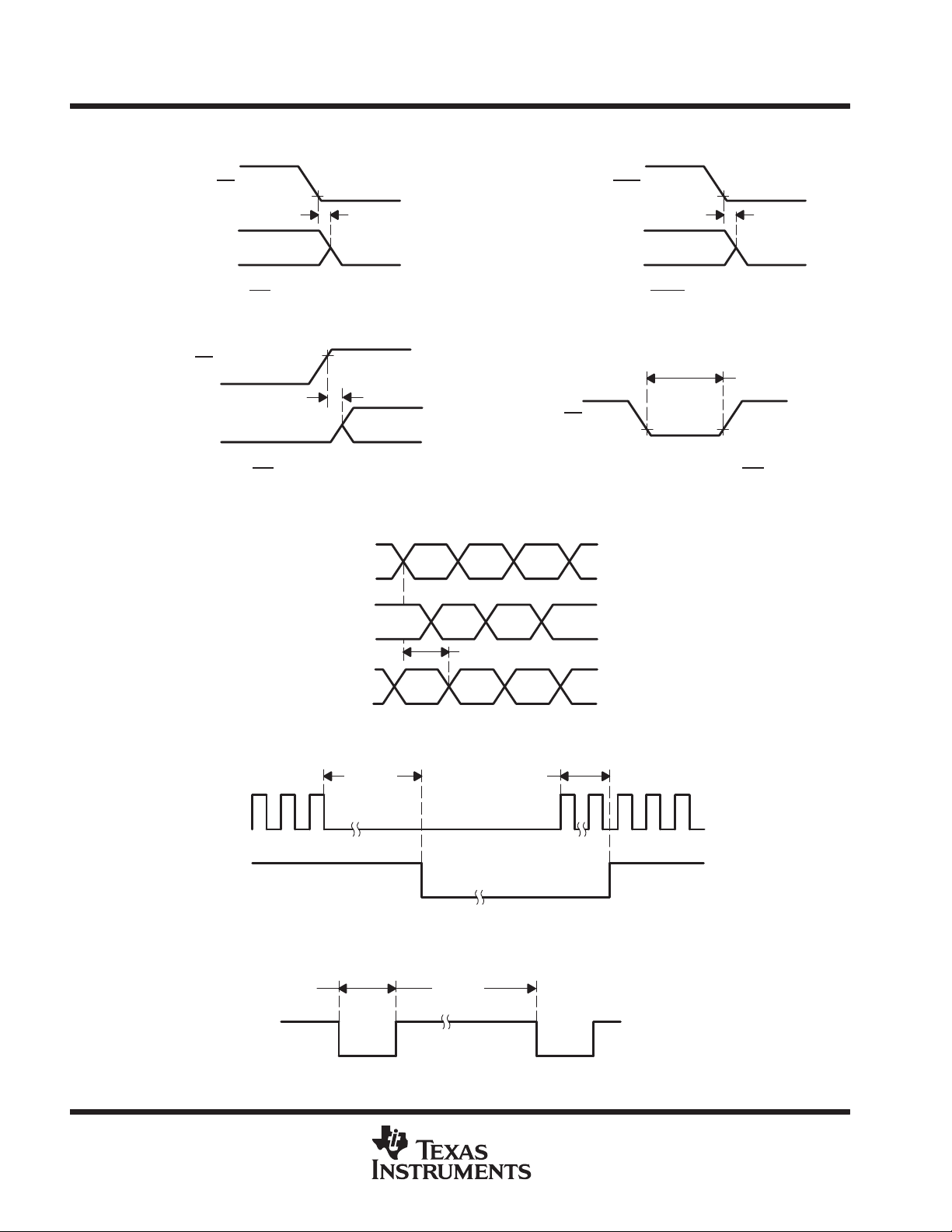
PARAMETER MEASUREMENT INFORMATION
DE CTL(1-3), HSYNC,
Figure 2. Rise and Fall TIme of Data and Control Signals
ODCK
DE CTL(1-3), HSYNC, VSYNC
ODCK
t
r2
20%
80%
t
f2
80%
20%
Figure 1. Rise and Fall Time of ODCK
t
r1
80% 80%
VSYNC
ODCK
20% 20%
f
ODCK
Figure 3. ODCK Frequency
t
(su1)
V
OH
V
OL
V
OH
V
OL
V
OH
V
OL
t
(h1)
t
(su2)
t
f1
t
(h2)
V
OH
V
OL
V
OH
V
OL
V
OH
V
OL
OCK_INV
Figure 4. Data Setup and Hold Time to Rising and Falling Edge of ODCK
V
50%
OH
t
d(st)
ODCK
QE(O-23)
Figure 5. ODCK High to QE[23:0]
Staggered Data Output
Figure 6. Analog Input Intra-Pair
POST OFFICE BOX 655303 • DALLAS, TEXAS 75265
Tx+
50%
Tx-
Differential Skew
t
ps
9
TFP9431
PanelBus DVI RECEIVER WITH TRIPLE DAC
SLDS122A – MARCH 2000 – REVISED JUNE 2000
PARAMETER MEASUREMENT INFORMATION
PD
ODCK, DE, CTL(1-3),
HSYNC, VSYNC, SCDT
V
IL
t
pd(PDL)
ODCK, DE, CTL(2-3),
HSYNC, VSYNC
PDO
V
IL
t
pd(PDOL)
Figure 7. Delay From PD Low to Hi-Z Outputs Figure 8. Delay From PDO Low to Hi-Z Outputs
V
PD
t
Rx(0-2)+, Rx(0-2)-,
DFO, ST,
OCK_INV
p(PDH-V)
Figure 9. Delay From PD Low to High Before
IH
t
wL(PDL_MIN)
PD
V
IL
Figure 10. Minimum Time PD Low
Inputs are Active
TX2
TX1
50%
t
ccs
50%
TX0
Figure 11. Analog Input Channel-to-Channel Skew
DE
SCDT
t
t(HSC)
t
t(FSC)
Figure 12. Time Between DE Transitions to SCDT Low and SCDT High
DE
t
DEL
t
DEH
Figure 13. Minimum DE Low and Maximum DE High
10
POST OFFICE BOX 655303 • DALLAS, TEXAS 75265

PanelBus DVI RECEIVER WITH TRIPLE DAC
SLDS122A – MARCH 2000 – REVISED JUNE 2000
detailed description
fundamental operation
The TFP9431 is a digital visual interface (DVI) compliant TMDS digital receiver that is used in digital display
systems to receive and decode TMDS encoded RGB pixel data streams and provide analog output. In a digital
display system a host, usually a PC or workstation, contains a DVI compatible transmitter that receives 24 bit
pixel data along with appropriate control signals. The transmitter encodes them into a high-speed low-voltage
differential serial bit stream optimized for transmission over a twisted-pair cable to a display device. The display
device, usually a CRT monitor , will require a DVI compatible receiver like the TI TFP9431 to decode the serial
bit stream back to the same 24 bit pixel data and control signals that originated at the host. This decoded data
is then converted to analog signals using a triple high-speed digital-to-analog converter (DAC) optimized for use
in video/graphics applications. The analog signals can be applied directly to the CRT drive circuitry to produce
an image on the display . Since the host and display can be separated by distances up to 5 meters or more, serial
transmission of the pixel data is preferred. T o support modern display resolutions up to UXGA a high bandwidth
receiver with good jitter and skew tolerance is required.
TMDS pixel data and control signal encoding
TMDS stands for transition minimized differential signaling. Only one of two possible TMDS characters for a
given pixel will be transmitted at a given time. The transmitter keeps a running count of the number of ones and
zeros previously sent and transmits the character that will minimize the number of transitions and approximate
a dc balance of the transmission line.
TFP9431
Three TMDS channels are used to receive RGB pixel data during active display time, DE = high. The same three
channels also receive control signals, HSYNC, VSYNC, and user defined control signals CTL[3:1]. These
control signals are received during inactive display or blanking-time. Blanking-time is when DE = low. The
following table maps the received input data to appropriate TMDS input channel in a DVI compliant system.
RECEIVED PIXEL DATA
ACTIVE DISPLAY DE = HIGH
Red[7:0] Channel – 2 (Rx2 ±)
Green[7:0] Channel – 1 (Rx1 ±)
Blue[7:0] Channel – 0 (Rx0 ±)
RECEIVED CONTROL DATA
BLANKING DE = LOW
CTL[3:2] Channel – 2 (Rx2 ±) CTL[3:2]
CTL[1: 0] (see Note 6) Channel – 1 (Rx1 ±) CTL1
HSYNC, VSYNC Channel – 0 (Rx0 ±) HSYNC, VSYNC
NOTE 7: Some TMDS transmitters transmit a CTL0 signal. The TFP9431 decodes and
transfers CTL[3:1] and ignores CTL0 characters. CTL0 is not available as a TFP9431
output.
INPUT CHANNEL
INPUT CHANNEL
OUTPUT PINS
(VALID FOR DE = HIGH)
OUTPUT PINS
(VALID FOR DE = LOW)
The TFP9431 discriminates between valid pixel TMDS characters and control TMDS characters to determine
the state of active display versus blanking, i.e., state of DE.
POST OFFICE BOX 655303 • DALLAS, TEXAS 75265
11

TFP9431
PanelBus DVI RECEIVER WITH TRIPLE DAC
SLDS122A – MARCH 2000 – REVISED JUNE 2000
detailed description (continued)
TFP9431 clocking and data synchronization
The TFP9431 receives a clock reference from the DVI transmitter that has a period equal to the pixel time, Tpix.
The frequency of this clock is also referred to as the pixel rate. Since the TMDS encoded data on Rx[2:0]
contains 10 bits per 8 bit pixel it follows that the Rx[2:0] serial bit rate is 10 times the pixel rate. For example,
the required pixel rate to support an UXGA resolution with 60 Hz refresh rate is 165 MHz. The TMDS serial bit
rate is 10x the pixel rate or 1.65 Gb/s. Due to the transmission of this high-speed digital bit stream, on three
separate channels (or twisted-pair wires) of long distances (3-5 meters), phase synchronization between the
data steams and the input reference clock is not guaranteed. In addition, skew between the three data channels
is common. The TFP9431 uses a 4x oversampling scheme of the input data streams to achieve reliable
synchronization with up to 1-Tpix channel-to-channel skew tolerance. Accumulated jitter on the clock and data
lines due to reflections and external noise sources is also typical of high speed serial data transmission, hence
the TFP9431’s design for high jitter tolerance.
The input clock to the TFP9431 is conditioned by a phase-locked-loop (PLL) to remove high frequency jitter from
the clock. The PLL provides four 10x clock outputs of different phase to locate and sync the TMDS data streams
(4x oversampling). During active display the pixel data is encoded to be transitioned minimized, whereas in
blank, the control data is encoded to be transition maximized. A DVI compliant transmitter is required to transmit
in blank for a minimum period of time, 128-Tpix, to ensure sufficient time for data synchronization when the
receiver sees a transition maximized code. Synchronization during blank, when the data is transition
maximized, ensures reliable data bit boundary detection. Phase synchronization to the data streams is unique
for each of the three input channels and is maintained as long as the link remains active.
TFP9431 TMDS input levels and input impedance matching
The TMDS inputs to the TFP9431 receiver have a fixed single-ended termination to AV
internally optimized using a laser trim process to precisely fix the impedance at 50 Ω. The device will function
normally with or without a resistor on the EXT_RES pin, so it remains drop-in compatible with current sockets.
The fixed impedance eliminates the need for an external resistor while providing optimum impedance matching
to standard 50-Ω DVI cables.
Figure 14 shows a conceptual schematic of a DVI transmitter and TFP9431 receiver connection. A transmitter
drives the twisted pair cable via a current source, usually achieved with an open drain type output driver. The
internal resistor, which is matched to the cable impedance, at the TFP9431 input provides a pullup to AV
Naturally , when the transmitter is disconnected and the TFP9431 DVI inputs are left unconnected, the TFP9431
receiver inputs pull-up to A V
15. The TFP9431 is designed to respond to differential signal swings ranging from 150 mV to 1.56 V with
common mode voltages ranging from (AVCC-300 mV) to (AVCC-37 mV).
. The single ended differential signal and full differential signal is shown in Figure
CC
The TFP9431 is
CC
CC
.
12
POST OFFICE BOX 655303 • DALLAS, TEXAS 75265

PanelBus DVI RECEIVER WITH TRIPLE DAC
detailed description (continued)
TFP9431 TMDS input levels and input impedance matching (continued)
DVI
Transmitter
DVI Compliant Cable
TFP9431
SLDS122A – MARCH 2000 – REVISED JUNE 2000
TI TFP9431
Receiver
AVCC
Internal
Termination at 50 Ω
DATA
AVCC
AVCC - 1/2 VIDIFF
DATA
Current
Source
Figure 14. TMDS Differential Input and Transmitter Connection
1/2 VIDIFF
a ) Single-Ended Input Signal
+ 1/2 VIDIFF
- 1/2 VIDIFF
b) Differential Input Signal
Figure 15. TMDS Inputs
+
_
VIDIFF
POST OFFICE BOX 655303 • DALLAS, TEXAS 75265
13

TFP9431
PanelBus DVI RECEIVER WITH TRIPLE DAC
SLDS122A – MARCH 2000 – REVISED JUNE 2000
detailed description (continued)
TFP9431 incorporates HSYNC jitter immunity
Several DVI transmitters available in the market introduce jitter on the transmitted HSYNC and VSYNC signals
during the TMDS encryption process. The HSYNC signal can shift by one pixel position (one clock) from nominal
in either direction, resulting in up to two cycles of HSYNC shift. This jitter carries through to the DVI receiver,
and if the position of HSYNC shifts continuously , the receiver can lose track of the input timing and pixel noise
will occur on the display. This jitter problem has been shown to be extremely visible on 1280 x 1024 at 85 Hz
CRT monitors and other DVI displays. For this reason, a DVI compliant receiver with HSYNC jitter immunity
should be used in all displays that could be connected to host PCs with transmitters that have this HSYNC jitter
problem.
The TFP9431 integrates HSYNC regeneration circuitry that provides a seamless interface to these
noncompliant transmitters. The position of the data enable (DE) signal is always fixed in relation to data,
irrespective of the location of HSYNC. The TFP9431 receiver uses the DE and clock signals recreate stable
vertical and horizontal sync signals. The circuit filters the HSYNC output of the receiver, and HSYNC is shifted
to the nearest eighth bit boundary , producing a stable output with respect to data, as shown in Figure 16. This
will ensure accurate data synchronization at the input of the display timing controller.
This HSYNC regeneration circuit is transparent to the monitor and need not be removed even if the transmitted
HSYNC is stable. For example, the PanelBus line of DVI 1.0 compliant transmitters, such as the TFP6422
and TFP420, do not have the HSYNC jitter problem. The TFP9431 will operate correctly with either compliant
or noncompliant transmitters.
ODCK
HSYNC IN
DE
HSYNC OUT
HSYNC Shift by ± 1 Clock
Figure 16. HSYNC Regeneration Timing Diagram
14
POST OFFICE BOX 655303 • DALLAS, TEXAS 75265

PanelBus DVI RECEIVER WITH TRIPLE DAC
SLDS122A – MARCH 2000 – REVISED JUNE 2000
TFP9431 modes of operation
The TFP9431 provides systems design flexibility and value by providing the system designer with configurable
options or modes of operation to support varying system architectures. The following table outlines the various
panel modes that can be supported.
TFP9431
PANEL PIXEL RATE
TFT or 16-bit DSTN 1 pix/clock Falling Free run 0 0 0
TFT or 16-bit DSTN 1 pix/clock Rising Free run 0 0 1
24-bit DSTN 1 pix/clock Falling Gated low 1 0 0
NONE 1 pix/clock Rising Gated low 1 0 1
ODCK LATCH
EDGE
ODCK DFO PIXS OCK_INV
TFP9431 output driver configurations
The TFP9431 provides flexibility by offering various output driver features that can be used to optimize power
consumption, ground-bounce and power-supply noise. The following sections outline the output driver features
and their effects.
Output driver power down (PDO
= low), Pulling PDO low will place all the output drivers, except CTL1 and
SCDT, into a high-impedance state and the DAC outputs will be powered down. A weak pulldown
(approximately 10 µA) will gradually pull these Hi-Z outputs to a low level to prevent the outputs from floating.
The SCDT output which indicates link-disabled or link-inactive can be tied directly to the PDO input to disable
the output drivers when the link is inactive or when the cable is disconnected. An internal pullup on the PDO
pin will default the TFP9431 to the normal nonpower down output drive mode if left unconnected.
Drive Strength (ST = high for high drive strength, ST=low for low drive strength.) The TFP9431 allows for
selectable output drive strength on the data, control and ODCK outputs. See the dc specifications table for the
values of I
and IOL current drives for a given ST state. The high output strength offers approximately two times
OH
the drive as the low output drive strength.
Power Management. The TFP9431 offers several system power management features. The following table
outlines the basic TFP9431 power modes.
POWER MODE I
Normal Mode
PIX = Low
Normal Mode
PIX = High
Power Down
= Low
PD
Output driver power down PDO= Low TBD • Cable connected and link is inactive (Can use SCDT to drive PDO)
†
ICC is the calculated as the sum of all VDD power supply currents (AVCC, DVCC, OVCC, PVCC)
‡
Measured when cable is disconnected from inputs.
‡
†
DD
TBD Normal operation pixel rate = 165 MHz
TBD Normal operation pixel rate = 165 MHz
TBD • System power down.
1-pixel/clock
2-pixel/clock (ODCK = 82.5 MHz)
• All outputs are Hi-Z with a weak pulldown (10 µA) to ground
• All inputs are disabled except PD
• All outputs except SCDT and CTL1 are Hi-Z with a weak pulldown (10 µA) to ground.
NOTES
Both PDO and PD have internal pullups so if left unconnected they will default the TFP9431 to normal operating
modes.
The TFP9431 power down (PD = low) is a complete power down in that it powers down the digital core, the
analog circuitry , and output drivers. All output drivers are placed into a Hi-Z state with a weak pulldown (10 µA)
to ground. All inputs are disabled except for the PD input. The TFP9431 will not respond to any digital or analog
inputs until PD is pulled high.
POST OFFICE BOX 655303 • DALLAS, TEXAS 75265
15

TFP9431
PanelBus DVI RECEIVER WITH TRIPLE DAC
SLDS122A – MARCH 2000 – REVISED JUNE 2000
TFP9431 output driver configurations (continued)
Sync Detect. The TFP9431 offers an output, SCDT to indicate link activity . The TFP9431 monitors activity on
DE to determine if the link is active. When 1 million (1e6) pixel clock periods pass without a transition on DE,
the TFP9431 considers the link inactive and SCDT is driven low. While SCDT is low, if two DE transitions are
detected within 1600 pixel clock periods, the link will be considered active and SCDT is pulled high.
SCDT can be used to signal a system power management circuit to initiate a system power down when the link
is considered inactive. The SCDT can also be tied directly to the TFP9431 PDO input to power down the output
drivers when the link is inactive. It is not recommended to use the SCDT to drive the PD input since, once in
complete power-down, the analog inputs are ignored and the SCDT state will not change. An external system
power management circuit to drive PD is preferred.
TI PowerP AD 64-TQFP package
The TFP9431 is packaged in TI’s thermally enhanced PowerPAD 64 TQFP packaging. The PowerPAD
package is a 10 mm × 10 mm × 1.4 mm TQFP outline with 0.5mm lead-pitch. The PowerPAD package has
a specially designed die mount pad that offers improved thermal capability over typical TQFP packages of the
same outline. The TI 64-TQFP PowerPAD package offers a back-side solder plane that connects directly to
the die mount pad for enhanced thermal conduction. The system designer has the option to solder this back
side plane to a thermal/ground plane on the PCB. Since the die pad is electrically connected to the TFP9431
chip substrate and hence ground, the back side PowerPAD connection to a PCB ground plane can improve
ground bounce and power-supply noise.
The connection of the PowerPAD to a PCB thermal/ground plane is purely optional.
Table 1 outlines the thermal properties of the TI 64-TQFP PowerPAD package. The 64-TQFP non-
PowerPAD package is included only for reference.
Table 1. TI 64-TQPF (10 × 10 × 1.4 mm)/0.5 mm Lead Pitch
PARAMETER
Theta-JA
Theta-JC
Maximum power dissipation
Maximum TFP401/401A pixel rate TBD TBD TBD
†
‡
§
†,‡
†,‡
†,‡,§
Specified with 2 oz. Cu PCB plating.
Airflow is at 0 LFM (no airflow)
Measured at ambient temperature, TA = 70°C.
WITHOUT
PowerPAD
45°C/W 27.3°C/W 17.3°C/W
3.11°C/W 0.12°C/W 0.12°C/W
1.6 W 2.7 W 4.3 W
PowerPAD
NOT CONNECTED TO PCB
THERMAL PLANE
PowerPAD
CONNECTED TO PCB
THERMAL PLANE
†
16
POST OFFICE BOX 655303 • DALLAS, TEXAS 75265

TFP9431
PanelBus DVI RECEIVER WITH TRIPLE DAC
SLDS122A – MARCH 2000 – REVISED JUNE 2000
MECHANICAL DATA
PAP (S-PQFP-G64) PowerPAD PLASTIC QUAD FLATPACK
49
64
1,05
0,95
0,50
48
0,27
0,17
33
32
17
1
7,50 TYP
10,20
SQ
9,80
12,20
SQ
11,80
16
M
0,08
Seating Plane
Thermal Pad
(See Note D)
0,15
0,05
0,13 NOM
Gage Plane
0,25
0°–7°
0,75
0,45
1,20 MAX
NOTES: A. All linear dimensions are in millimeters.
B. This drawing is subject to change without notice.
C. Body dimensions do not include mold flash or protrusion.
D. The package thermal performance may be enhanced by bonding the thermal pad to an external thermal plane.
This pad is electrically and thermally connected to the backside of the die and possibly selected leads.
E. Falls within JEDEC MS-026
PowerPAD is a trademark of Texas Instruments.
POST OFFICE BOX 655303 • DALLAS, TEXAS 75265
0,08
4147702/A 01/98
17

IMPORTANT NOTICE
T exas Instruments and its subsidiaries (TI) reserve the right to make changes to their products or to discontinue
any product or service without notice, and advise customers to obtain the latest version of relevant information
to verify, before placing orders, that information being relied on is current and complete. All products are sold
subject to the terms and conditions of sale supplied at the time of order acknowledgment, including those
pertaining to warranty, patent infringement, and limitation of liability.
TI warrants performance of its semiconductor products to the specifications applicable at the time of sale in
accordance with TI’s standard warranty. Testing and other quality control techniques are utilized to the extent
TI deems necessary to support this warranty . Specific testing of all parameters of each device is not necessarily
performed, except those mandated by government requirements.
Customers are responsible for their applications using TI components.
In order to minimize risks associated with the customer’s applications, adequate design and operating
safeguards must be provided by the customer to minimize inherent or procedural hazards.
TI assumes no liability for applications assistance or customer product design. TI does not warrant or represent
that any license, either express or implied, is granted under any patent right, copyright, mask work right, or other
intellectual property right of TI covering or relating to any combination, machine, or process in which such
semiconductor products or services might be or are used. TI’s publication of information regarding any third
party’s products or services does not constitute TI’s approval, warranty or endorsement thereof.
Copyright 2000, Texas Instruments Incorporated
 Loading...