

TCM29C13, TCM29C14, TCM29C16, TCM29C17,
TCM129C13, TCM129C14, TCM129C16, TCM129C17
COMBINED SINGLE-CHIP PCM CODEC AND FILTER
SCTS011H – APRIL 1986 – REVISED JULY 1996
1
POST OFFICE BOX 655303 • DALLAS, TEXAS 75265
D
Replaces Use of TCM2910A in Tandem With
TCM2912C
D
Reliable Silicon-Gate CMOS Technology
D
Low Power Consumption:
Operating Mode...80 mW Typical
Power-Down Mode...5 mW Typical
D
Excellent Power-Supply Rejection Ratio
Over Frequency Range of 0 Hz to 50 kHz
D
No External Components Needed for
Sample, Hold, and Autozero Functions
D
Precision Internal Voltage References
D
Direct Replacement for Intel 2913, 2914,
2916, and 2917
D
Recommended for Direct V oice
Applications
description
The TCM29C13, TCM29C14, TCM29C16,
TCM29C17, TCM129C13, TCM129C14, TCM129C16, and TCM129C17 are single-chip PCM codecs
(pulse-code-modulated encoders and decoders) and PCM line filters. They provide all the functions required
to interface a full-duplex (4-wire) voice telephone circuit with a TDM (time-division-multiplexed) system, and are
intended to replace the TCM2910A in tandem with the TCM2912C. Primary applications include:
• Line interface for digital transmission and switching of T1 carrier, PABX, and central office telephone
systems
• Subscriber line concentrators
• Digital-encryption systems
• Digital voice-band data-storage systems
• Digital signal processing
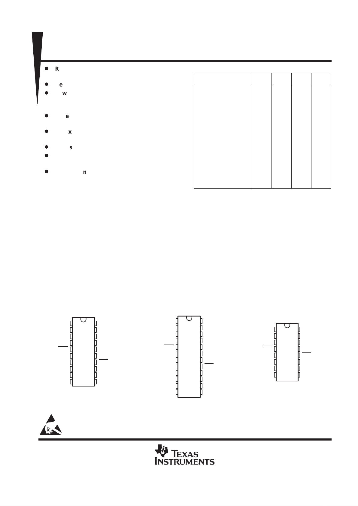
1
2
3
4
5
6
7
8
16
15
14
13
12
11
10
9
V
BB
PWRO+
PWRO–
PDN
DCLKR
PCM IN
FSR/TSRE
DGTL GND
V
CC
GSX
ANLG IN–
ANLG GND
TSX/DCLKX
PCM OUT
FSX/TSXE
CLKR/CLKX
TCM29C16, TCM29C17,
TCM129C16, TLC129C17
DW OR N PACKAGE
(TOP VIEW)
1
2
3
4
5
6
7
8
9
10
20
19
18
17
16
15
14
13
12
11
V
BB
PWRO+
PWRO–
GSR
PDN
CLKSEL
DCLKR
PCM IN
FSR/TSRE
DGTL GND
V
CC
GSX
ANLG IN–
ANLG IN+
ANLG GND
SIGX/ASEL
TSX/DCLKX
PCM OUT
FSX/TSXE
CLKR/CLKX
TCM29C13, TCM129C13
DW OR N PACKAGE
(TOP VIEW)
1
2
3
4
5
6
7
8
9
10
11
12
24
23
22
21
20
19
18
17
16
15
14
13
V
BB
PWRO+
PWRO–
GSR
PDN
CLKSEL
ANLG LOOP
SIGR
DCLKR
PCM IN
FSR/TSRE
DGTL GND
V
CC
GSX
ANLG IN–
ANLG IN+
ANLG GND
NC
SIGX/ASEL
TSX
/DCLKX
PCM OUT
FSX/TSXE
CLKX
CLKR
TCM29C14, TCM129C14
DW PACKAGE
(TOP VIEW)
NC – No internal connection
These devices have limited built-in ESD protection. The leads should be shorted together or the device placed in conductive foam
during storage or handling to prevent electrostatic damage to the MOS gates.
Copyright 1996, Texas Instruments Incorporated
PRODUCTION DATA information is current as of publication date.
Products conform to specifications per the terms of Texas Instruments
standard warranty. Production processing does not necessarily include
testing of all parameters.
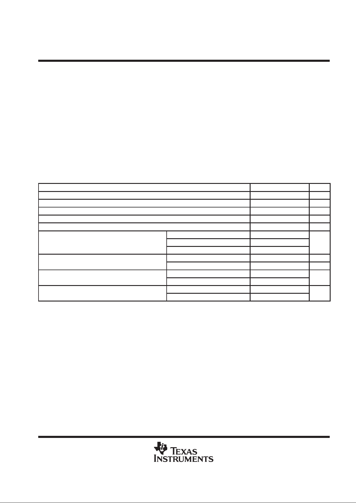
Number of Pins:
24 X
20 X
16 X X
µ-Law/A-Law Coding:
µ-Law X X X
A-Law X X X
Gain Timing Rates:
Variable Mode
64 kHz to 2.048 MHz X X X X
Fixed Mode
1.536 MHz X X
1.544 MHz X X
2.048 MHz X X X X
Loopback Test Capability X
8th-Bit Signaling X
FEATURES TABLE
FEATURE
29C13
129C13
29C14
129C14
29C16
129C16
29C17
129C17
TCM29C13, TCM29C14, TCM29C16, TCM29C17,
TCM129C13, TCM129C14, TCM129C16, TCM129C17
COMBINED SINGLE-CHIP PCM CODEC AND FILTER
SCTS011H – APRIL 1986 – REVISED JULY 1996
2
POST OFFICE BOX 655303 • DALLAS, TEXAS 75265
description (continued)
These devices are designed to perform the transmit encoding (A/D conversion) and receive decoding (D/A
conversion) as well as the transmit and receive filtering functions in a pulse-code-modulated system. They are
intended to be used at the analog termination of a PCM line or trunk.
The TCM129C13, TCM129C14, TCM129C16, TCM129C17, TCM29C13, TCM29C14, TCM29C16, and
TCM29C17 provide the band-pass filtering of the analog signals prior to encoding and after decoding. These
combination devices perform the encoding and decoding of voice and call progress tones as well as the
signaling and supervision information.
The TCM29C13, TCM29C14, TCM29C16, and TCM29C17 are characterized for operation from 0°C to 70°C.
The TCM129C13, TCM129C14, TCM129C16, and TCM129C17 are characterized for operation from –40°C
to 85°C.
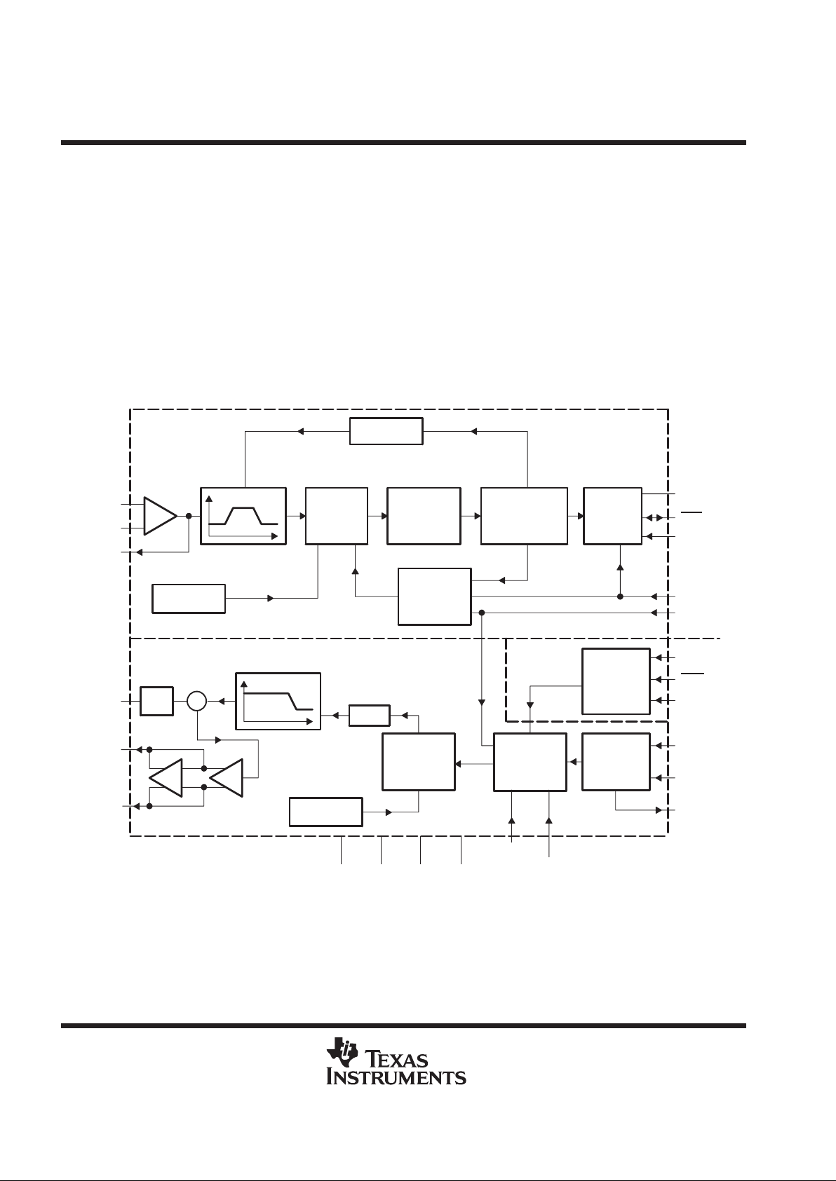
functional block diagram
Successive
Approximation
Buffer
PWRO+
PWRO–
GSR
GSX
ANLG IN–
ANLG IN+
Transmit Section
Receive Section
SIGR
†
Control
Section
PDN
Control
Logic
DCLKR
PCM IN
Input
Register
Digital-
to-Analog
Control
Logic
Reference
Sample
and Hold
and DAC
Analog-
to-Digital
Control
Logic
Gain
Set
Filter
Reference
FSX/TSXE
Autozero
Output
Register
TSX/DCLKX
PCM OUT
Comparator
Sample
and Hold
and DAC
Filter
SIGX/ASEL
CLKX
CLKSEL
ANLG
LOOP
†
FSR/TSRE
CLKR
†
ANLG
GND
DGTL
GND
V
BB
V
CC
‡
†
TCM29C14 and TCM129C14 only
‡
TCM29C13, TCM29C16, TCM29C17, TCM129C13, TCM129C16, and TCM129C17 only
TCM29C13, TCM29C14, TCM29C16, TCM29C17,
TCM129C13, TCM129C14, TCM129C16, TCM129C17
COMBINED SINGLE-CHIP PCM CODEC AND FILTER
SCTS011H – APRIL 1986 – REVISED JULY 1996
3
POST OFFICE BOX 655303 • DALLAS, TEXAS 75265
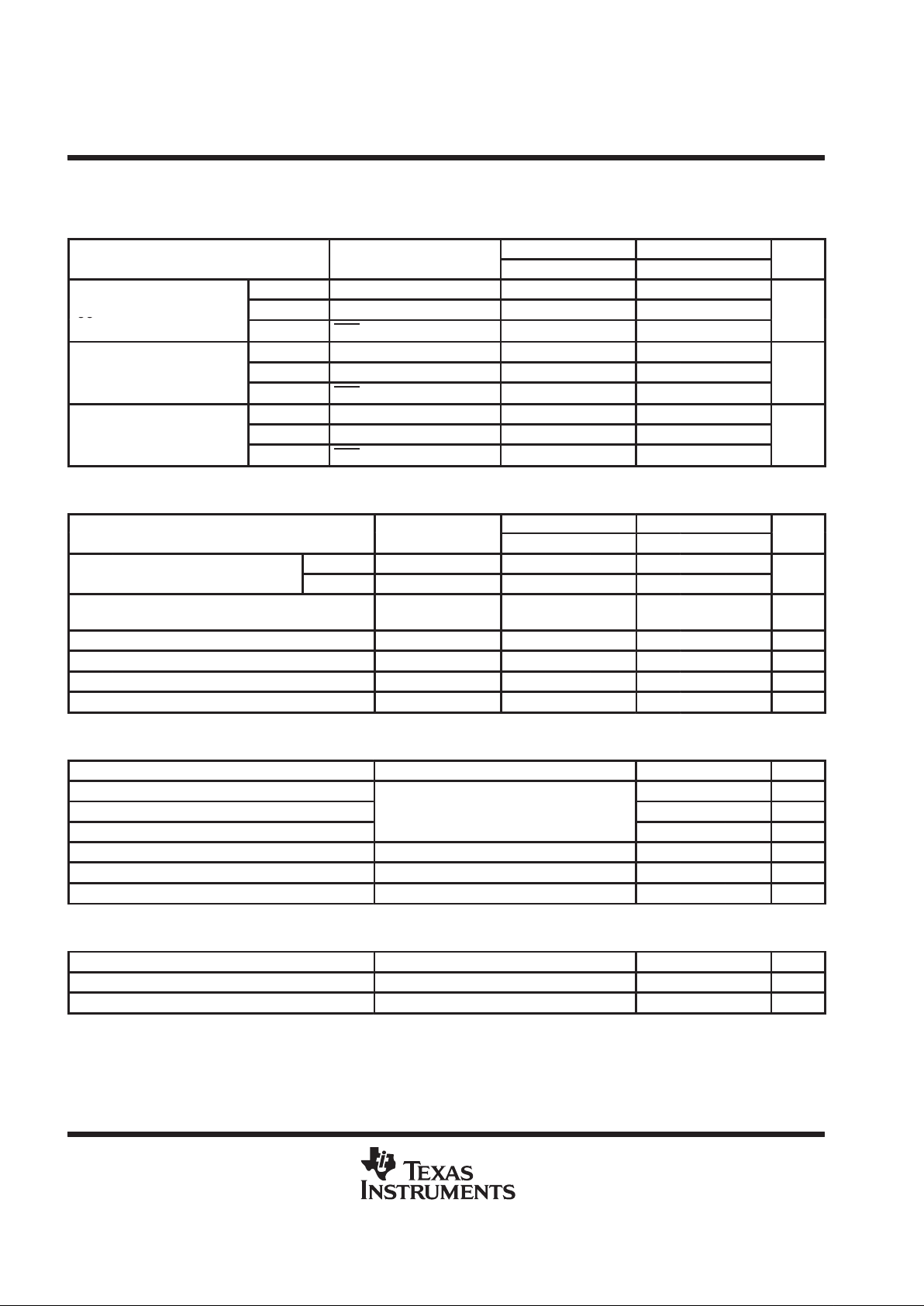
Terminal Functions
TERMINAL NO.
NAME
TCM29C13
TCM129C13
TCM29C14
TCM129C14
TCM29C16
TCM29C17
TCM129C16
TCM129C17
I/O DESCRIPTION
ANLG GND 16 20 13 Analog ground return for all internal voice circuits. Not internally
connected to DGTL GND.
ANLG IN+ 17 21 I Noninverting analog input to uncommitted transmit operational amplifier .
Internally connected to ANLG GND on TCM129C16, TCM29C16,
TCM129C17, and TCM29C17.
ANLG IN– 18 22 14 I Inverting analog input to uncommitted transmit operational amplifier.
ANLG LOOP 7 I Provides loopback test capability. When this input is high, PWRO + is
internally connected to ANLG IN.
CLKR 11 13 9 I Receive master clock and data clock for the fixed-data-rate mode.
Receive master clock only for variable-data-rate mode. CLKR and CLKX
are internally connected together for TCM129C13, TCM129C16,
TCM129C17, TCM29C13, TCM29C16, and TCM29C17.
CLKSEL 6 6 I Clock-frequency selection. Input must be connected to VBB, VCC, or
ground to reflect the master-clock frequency . When tied to VBB, CLK is
2.048 MHz. When tied to GND, CLK is 1.544 MHz. When tied to VCC,
CLK is 1.536 MHz.
CLKX 11 14 9 I Transmit master clock and data clock for the fixed-data-rate mode.
Transmit master clock only for variable-date-rate mode. CLKR and
CLKX are internally connected for the TCM129C13, TCM129C16,
TCM129C17, TCM29C13, TCM29C16, and TCM29C17.
DCLKR 7 9 5 I Fixed or variable-data-rate operation select. When connected to VBB,
the device operates in the fixed-data-rate mode. When DCLKR is not
connected to VBB, the device operates in the variable-data-rate mode,
and DCLKR becomes the receiver data clock. DCLKR then operates at
frequencies from 64 kHz to 2.048 MHz.
DGTL GND 10 12 8 Digital ground for all internal logic circuits. Not internally connected to
ANLG GND.
FSR/TSRE 9 11 7 I Frame synchronization clock input/time-slot enable for receive channel.
In the fixed-data-rate mode, FSR distinguishes between signaling and
nonsignaling frames by a double- or single-length pulse, respectively . In
the variable-data-rate mode, this signal must remain high for the duration
of the time slot. The receive channel enters the standby state when FSR
is TTL low for 300 ms.
FSX/TSXE 12 15 10 I Frame-synchronization clock input/time-slot enable for transmit
channel. Operates independently of, but in an analagous manner to,
FSR/TSRE. The transmit channel enters the standby state when FSX is
low for 300 ms.
GSR 4 4 I Input to the gain-setting network on the output power amplifier.
Transmission level can be adjusted over a 12-dB range depending on the
voltage at GSR.
GSX 19 23 15 O Output terminal of internal uncommitted operational amplifier . Internally ,
this is the voice signal input to the transmit filter.
PCM IN 8 10 6 I Receive PCM input. PCM data is clocked in on eight consecutive
negative transitions of the receive data clock, which is CLKR in
fixed-data-rate timing and DCLKR in variable-data-rate timing.
PCM OUT 13 16 11 O Transmit PCM output. PCM data is clocked out on this output on eight
consecutive positive transitions of the transmit data clock, which is CLKX
in fixed-data-rate timing and DCLKX in variable-data-rate timing.
TCM29C13, TCM29C14, TCM29C16, TCM29C17,
TCM129C13, TCM129C14, TCM129C16, TCM129C17
COMBINED SINGLE-CHIP PCM CODEC AND FILTER
SCTS011H – APRIL 1986 – REVISED JULY 1996
4
POST OFFICE BOX 655303 • DALLAS, TEXAS 75265
Terminal Functions
TERMINAL NO.
NAME
TCM29C13
TCM129C13
TCM29C14
TCM129C14
TCM29C16
TCM29C17
TCM129C16
TCM129C17
I/O DESCRIPTION
PDN 5 5 4 I Power-down select. The device is inactive with a TTL low-level input to
this terminal and active with a TTL high-level input to the terminal.
PWRO+ 2 2 2 O Noninverting output of power amplifier. Can drive transformer hybrids or
high-impedance loads directly in either a differential or a single-ended
configuration
PWRO– 3 3 3 O Inverting output of power amplifier. Functionally identical with and
complementary to PWRO+.
SIGR 8 O Signaling bit output, receive channel. In a fixed-data-rate mode, outputs
the logical state of the 8th bit (LSB) of the PCM word in the most recent
signaling frame.
SIGX/ASEL 15 18 I A-law and µ-law operation select. When connected to VBB, A-law is
selected. When connected to VCC or GND, µ-law is selected. When not
connected to VBB, a TTL-level input is transmitted as the eighth bit (LBS)
of the PCM word during signaling frames on PCM OUT (TCM29C14 and
TCM129C14 only). SIGX/ASEL is internally connected to provide µ-law
operational for TCM29C16 and TCM129C16 and A-law operation for
TCM29C17 and TCM129C17.
TSX/DCLKX 14 17 12 I/O Transmit channel time-slot strobe (output) or data clock (input) for the
transmit channel. In the fixed-data-rate mode, this terminal is an
open-drain output to be used as an enable signal for a 3-state output
buffer. In the variable-data rate mode, DCLKX becomes the transmit
data clock, which operates at TTL level from 64 kHz to 2.048 MHz.
V
BB
1 1 1 Most negative supply voltage. Input is –5 V ±5%.
V
CC
20 24 16 Most positive supply voltage. Input is 5 V ±5%
TCM29C13, TCM29C14, TCM29C16, TCM29C17,
TCM129C13, TCM129C14, TCM129C16, TCM129C17
COMBINED SINGLE-CHIP PCM CODEC AND FILTER
SCTS011H – APRIL 1986 – REVISED JULY 1996
5
POST OFFICE BOX 655303 • DALLAS, TEXAS 75265
absolute maximum ratings over operating free-air temperature range (unless otherwise noted)
†
Supply voltage range, V
CC
(see Note 1) –0.3 V to 15 V. . . . . . . . . . . . . . . . . . . . . . . . . . . . . . . . . . . . . . . . . . . . .
Output voltage range, V
O
–0.3 V to 15 V. . . . . . . . . . . . . . . . . . . . . . . . . . . . . . . . . . . . . . . . . . . . . . . . . . . . . . . . . .
Input voltage range, V
I
–0.3 V to 15 V. . . . . . . . . . . . . . . . . . . . . . . . . . . . . . . . . . . . . . . . . . . . . . . . . . . . . . . . . . . . .
Digital ground voltage range –0.3 V to 15 V. . . . . . . . . . . . . . . . . . . . . . . . . . . . . . . . . . . . . . . . . . . . . . . . . . . . . . . .
Continuous total dissipation at (or below) 25°C free-air temperature 1375 mW. . . . . . . . . . . . . . . . . . . . . . . . .
Operating free-air temperature range, T
A
: TCM29Cxx 0°C to 70°C. . . . . . . . . . . . . . . . . . . . . . . . . . . . . . . . . .
TCM129Cxx –40°C to 85°C. . . . . . . . . . . . . . . . . . . . . . . . . . . . . . .
Storage temperature range, T
stg
–65°C to 150°C. . . . . . . . . . . . . . . . . . . . . . . . . . . . . . . . . . . . . . . . . . . . . . . . . . .
Lead temperature 1,6 mm (1/16 inch) from case for 10 seconds: DW or N package 260°C. . . . . . . . . . . . . .
†
Stresses beyond those listed under “absolute maximum ratings” may cause permanent damage to the device. These are stress ratings only, and
functional operation of the device at these or any other conditions beyond those indicated under “recommended operating conditions” is not
implied. Exposure to absolute-maximum-rated conditions for extended periods may affect device reliability.
NOTE 1: Voltage values for maximum ratings are with respect to VBB.
recommended operating conditions (see Note 2)
MIN NOM MAX UNIT
Supply voltage, VCC (see Note 3) 4.75 5 5.25 V
Supply voltage, V
BB
–4.75 –5 –5.25 V
Digital ground voltage with respect to ANGL GND 0 V
High-level input voltage, VIH (all inputs except CLKSEL) 2.2 V
Low-level input voltage, VIL (all inputs except CLKSEL) 0.8 V
2.048 MHz V
BB
VBB +0.5
Clock-select input voltage
1.544 MHz 0 0.5
V
1.536 MHz VCC –0.5 V
CC
GSX 10 kΩ
Load resistance, R
L
PWRO+ and/or PWRO– 300 Ω
p
GSX 50
p
Load capacitance, C
L
PWRO+ and/or PWRO– 100
pF
p
p
TCM29Cxx 0 70
°
Operating free-air temperature, T
A
TCM129Cxx –40 85
°C
NOTES: 2. T o avoid possible damage to these CMOS devices and resulting reliability problems, the power-up procedure described in the device
power-up sequence paragraphs later in this document should be followed.
3. V oltage at analog inputs and outputs, VCC and VBB terminals, are with respect to the ANLG GND terminal. All other voltages are
referenced to the digital ground terminal unless otherwise noted.
TCM29C13, TCM29C14, TCM29C16, TCM29C17,
TCM129C13, TCM129C14, TCM129C16, TCM129C17
COMBINED SINGLE-CHIP PCM CODEC AND FILTER
SCTS011H – APRIL 1986 – REVISED JULY 1996
6
POST OFFICE BOX 655303 • DALLAS, TEXAS 75265
electrical characteristics over recommended ranges of supply voltage and operating free-air
temperature (unless otherwise noted)
supply current, f
DCLK
= 2.048 MHz, outputs not loaded
TCM29Cxx TCM129Cxx
PARAMETER
TEST CONDITIONS
MIN TYP†MAX MIN TYP†MAX
UNIT
Operating 7 9 8 13
I
CC
Supply current
Standby FSX, FSR = VIL after 300 ms 0.5 1 0.7 1.5
mA
CC
from V
CC
Power down
PDN = VIL after 10 µs
0.3 0.8 0.4 1
Operating –7 –9 –8 –13
I
BB
Supply current
Standby FSX, FSR = VIL after 300 ms –0.5 –1 –0.7 –1.5
mA
BB
from V
BB
Power down
PDN = VIL after 10 µs
–0.3 –0.8 –0.4 –1
Operating 70 90 80 130
P
D
Power dissipation
Standby FSX, FSR = VIL after 300 ms 5 10 7 15
mW
Power down
PDN = VIL after 10 µs
3 8 4 10
†
All typical values are at VBB = –5 V , VCC = 5 V, and TA = 25°C.
digital interface
TCM29Cxx TCM129Cxx
PARAMETER
TEST CONDITIONS
MIN TYP†MAX MIN TYP†MAX
UNIT
p
PCM OUT IOH = –9.6 mA 2.4 2.4
VOHHigh-level output voltage
SIGR IOH = –1.2 mA 2.4 2.4
V
V
OL
Low-level output voltage at PCM OUT,
TSX, SIGR
IOL = 3.2 mA 0.4 0.5 V
I
IH
High-level input current, any digital input VI = 2.2 V to V
CC
10 12 µA
I
IL
Low-level input current, any digital input VI = 0 to 0.8 V 10 12 µA
C
i
Input capacitance 5 10 5 10 pF
C
o
Output capacitance 5 5 pF
†
All typical values are at VBB = –5 V , VCC = 5 V, and TA = 25°C.
transmit amplifier input
PARAMETER TEST CONDITIONS MIN TYP†MAX UNIT
Input current at ANLG IN+, ANLG IN – ±100 nA
Input offset voltage at ANLG IN+, ANLG IN –
VI = –2.17 V to 2.17 V
±25 mV
Common-mode rejection at ANLG IN +, ANLG IN – 55 dB
Open-loop voltage amplification at GSX 5000
Open-loop unity-gain bandwidth at GSX 1 MHz
Input current at ANLG IN+, ANLG IN – 10 MΩ
†
All typical values are at VBB = –5 V , VCC = 5 V, and TA = 25°C.
receive filter output
PARAMETER TEST CONDITIONS MIN TYP†MAX UNIT
Output offset voltage PWRO+, PWRO– (single ended) Relative to ANLG GND 80 180 mV
Output resistance at PWRO+, PWRO– 1 Ω
†
All typical values are at VBB = –5 V , VCC = 5 V, and TA = 25°C.
TCM29C13, TCM29C14, TCM29C16, TCM29C17,
TCM129C13, TCM129C14, TCM129C16, TCM129C17
COMBINED SINGLE-CHIP PCM CODEC AND FILTER
SCTS011H – APRIL 1986 – REVISED JULY 1996
7
POST OFFICE BOX 655303 • DALLAS, TEXAS 75265
gain and dynamic range, VCC = 5 V, VBB = 5 V, TA = 25°C (unless otherwise noted)
(see Notes 4, 5, and 6)
PARAMETER TEST CONDITIONS MIN TYP MAX UNIT
p
Signal input = 1.064 Vrms for µ-law,
Encoder milliwatt response (transmit gain tolerance)
g µ ,
Signal input = 1.068 Vrms for A-law
±
0.04±0.02
dBm0
Encoder milliwatt response additional tolerance
(nominal supplies and temperature)
TA = 0°C to 70°C, Supplies = ± 5% ± 0.08 dB
Digital milliwatt response (receive tolerance gain)
relative to zero-transmission-level point
Signal input per CCITT G.711,
Output signal = 1 kHz
±
0.04±0.02
dBm0
Digital milliwatt response variation with temperature
and supplies
TA = 0°C to 70°C, Supplies = ± 5% ±0.08 dB
µ-law
2.76
Zero-transmission-level point, transmit channel
A-law
R
L
=
600 Ω
2.79
,
(0 dBm0)
µ-law
1
dBm
A-law
R
L
=
900 Ω
1.03
µ-law
5.76
Zero-transmission-level point, receive channel
A-law
R
L
=
600 Ω
5.79
(0 dBm0)
µ-law
4
dBm
A-law
R
L
=
900 Ω
4.03
NOTES: 4. Unless otherwise noted, the analog input is a 0-dBm0, 1020-Hz sine wave, where 0 dBm0 is defined as the zero-reference point of
the channel under test. This corresponds to an analog signal input of 1.064 Vrms or an output of 1.503 Vrms.
5. The input amplifier is set for noninverting unity gain. The digital input is a PCM bit stream generated by passing a 0-dBm0, 1020-Hz
sine wave through an ideal encoder.
6. Receive output is measured single ended in the maximum gain configuration. To set the output amplifier for maximum gain, GSR is
connected to PWRO– and the output is taken at PWRO+. All output levels are (sin x)/x corrected.
gain tracking over recommended ranges of supply voltage and operating free-air temperature,
reference level = –10 dBm0
PARAMETER TEST CONDITIONS MIN MAX UNIT
3 ≥ input level ≥ –40 dBm0 ±0.25
Transmit gain-tracking error , sinusoidal input
–40 > input level ≥ –50 dBm0 ±0.5
dB
–50 > input level ≥ –55 dBm0 ±1.2
3 ≥ input level ≥ –40 dBm0 ±0.25
Receive gain-tracking error, sinusoidal input
–40 > input level ≥ –50 dBm0 ±0.5
dB
–50 > input level ≥ –55 dBm0 ±1.2
TCM29C13, TCM29C14, TCM29C16, TCM29C17,
TCM129C13, TCM129C14, TCM129C16, TCM129C17
COMBINED SINGLE-CHIP PCM CODEC AND FILTER
SCTS011H – APRIL 1986 – REVISED JULY 1996
8
POST OFFICE BOX 655303 • DALLAS, TEXAS 75265
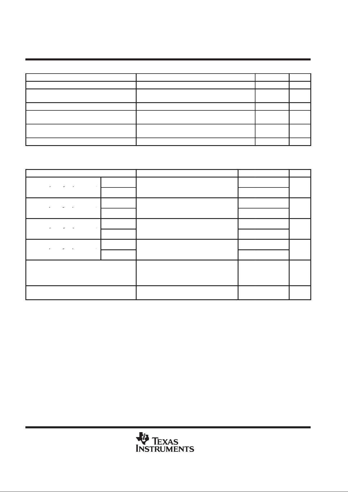
noise over recommended ranges of supply voltage and operating free-air temperature range
PARAMETER TEST CONDITIONS MIN MAX UNIT
Transmit noise, C-message weighted ANLG IN+ = ANLG GND, ANLG IN– = GSX 15 dBrnC0
Transmit noise, C-message weighted with 8-bit-
signaling (TCM29C14 and TCM129C14 only)
ANLG IN+ = ANLG GND, ANLG IN– = GSX,
6th frame signaling
18 dBrnC0
Transmit noise, psophometrically weighted ANLG IN+ = ANLG GND, ANLG IN– = GSX –69 dBm0p
Receive noise, C-message-weighted quiet code
PCM IN = 11111111 (µ-law), PCM IN = 10101010
(A-law), measured at PWRO+
11 dBrnC0
Receive noise, C-message-weighted sign bit toggled
Input to PCM IN is zero code with sign bit toggled at
1-kHz rate
12 dBrmC0
Receive noise, psophometrically weighted PCM = lowest positive decode level –79 dBm0p
power-supply rejection ratio and crosstalk attenuation over recommended ranges of supply
voltage and operating free-air temperature
PARAMETER TEST CONDITIONS MIN TYP†MAX UNIT
V
supply-voltage rejection ratio,
0 ≤ f < 30 kHz
Idle channel,
pp
–30
CC
ygj ,
transmit channel
30 ≤ f < 50 kHz
Supply signal
=
200 mV
(peak-to-peak)
,
f measured at PCM OUT
–45
dB
V
supply-voltage rejection ratio,
0 ≤ f < 30 kHz
Idle channel,
pp
–30
BB
ygj ,
transmit channel
30 ≤ f < 50 kHz
Supply signal
=
200 mV
(peak-to-peak)
,
f measured at PCM OUT
–55
dB
V
supply-voltage rejection ratio,
0 ≤ f < 30 kHz
Idle channel,
pp
–20
CC
ygj ,
receive channel (single ended)
30 ≤ f < 50 kHz
Supply signal
=
200 mV
(peak-to-peak)
,
f measured at PWRO+
–45
dB
V
supply-voltage rejection ratio,
0 ≤ f < 30 kHz
Idle channel,
pp
–20
BB
ygj ,
receive channel (single ended)
30 ≤ f < 50 kHz
Supply signal
=
200 mV
(peak-to-peak)
,
Narrow band, f measured at PWRO+
–45
dB
Crosstalk attenuation, transmit to receive
(single ended)
ANLG IN+ = 0 dBm0, f = 1.02 kHz,
Unity gain,
PCM IN = lowest decode level,
Measured at PWRO+
71 dB
Crosstalk attenuation, receive to transmit
(single ended)
PCM IN = 0 dBm0, f = 1.02 kHz,
Measured at PCM OUT
71 dB
†
All typical values are at VBB = –5 V , VCC = 5 V, and TA = 25°C.

TCM29C13, TCM29C14, TCM29C16, TCM29C17,
TCM129C13, TCM129C14, TCM129C16, TCM129C17
COMBINED SINGLE-CHIP PCM CODEC AND FILTER
SCTS011H – APRIL 1986 – REVISED JULY 1996
9
POST OFFICE BOX 655303 • DALLAS, TEXAS 75265
distortion over recommended ranges of supply voltage and operating free-air temperature
PARAMETER TEST CONDITIONS MIN TYP†MAX UNIT
0 dBm0 ≥ ANLG IN+ ≥ –30 dBm0 36
Transmit signal-to-distortion ratio, sinusoidal
p
–30 dBm0 > ANLG IN+ ≥ –40 dBm0 30
dB
in ut (CCITT G.712
–
Method 2)
–40 dBm0 > ANLG IN+ ≥ –45 dBm0 25
0 dBm0 ≥ ANLG IN+ ≥ –30 dBm0 36
Receive signal-to-distortion ratio, sinusoidal
p
–30 dBm0 > ANLG IN+ ≥ –40 dBm0 30
dB
in ut (CCITT G.712
–
Method 2)
–40 dBm0 > ANLG IN+ ≥ –45 dBm0 25
Transmit single-frequency distortion products AT&T Advisory #64 (3.8), Input signal = 0 dBm0 –46 dBm0
Receive single-frequency distortion products AT&T Advisory #64 (3.8), Input signal = 0 dBm0 –46 dBm0
CCITT G.712 (7.1) –35
Intermodulation distortion, end-to-end spurious
CCITT G.712 (7.2) –49
,
out-of-band signals, end-to-end
CCITT G.712 (6.1) –25
dBm0
CCITT G.712 (9) –40
Transmit absolute delay time to PCM OUT
Fixed-data rate, f
CLKX
+ 2.048 MHz,
Input to ANLG IN+ 1.02 kHz at 0 dBm0
245 µs
f = 500 Hz to 600 Hz 170
Transmit differential envelope delay time
f = 600 Hz to 1000 Hz 95
y
relative to transmit absolute delay time
f = 1000 Hz to 2600 Hz 45
µ
s
f = 2600 Hz to 2800 Hz 105
Receive absolute delay time to PWRO+
Fixed-data rate, f
CLKR
+ 2.048 MHz,
Digital input is DMW code
190 µs
f = 500 Hz to 600 Hz 45
Receive differential envelope delay time
f = 600 Hz to 1000 Hz 35
y
relative to transmit absolute delay time
f = 1000 Hz to 2600 Hz 85
µ
s
f = 2600 Hz to 2800 Hz 110
†
All typical values are at VBB = –5 V , VCC = 5 V, and TA = 25°C.
transmit filter transfer over recommended ranges of supply voltage and operating free-air
temperature (see Figure 1)
PARAMETER TEST CONDITIONS MIN MAX UNIT
f = 16.67 Hz –30
f = 50 Hz –25
f = 60 Hz –23
Input amplifier set for unity gain
,
f = 200 Hz –1.8 –0.125
Gain relative to gain at 1.02 kHz
In ut am lifier set for unity gain,
Noninverting maximum gain output,
f = 300 Hz to 3 kHz –0.15 0.15
dB
Input signal at ANLG IN+ is 0 dBm0
f = 3.3 kHz –0.35 0.15
f = 3.4 kHz –1 –0.1
f = 4 kHz –14
f = 4.6 kHz and above –32

TCM29C13, TCM29C14, TCM29C16, TCM29C17,
TCM129C13, TCM129C14, TCM129C16, TCM129C17
COMBINED SINGLE-CHIP PCM CODEC AND FILTER
SCTS011H – APRIL 1986 – REVISED JULY 1996
10
POST OFFICE BOX 655303 • DALLAS, TEXAS 75265
receive filter transfer over recommended ranges of supply voltage and operating free-air
temperature (see Figure 2)
PARAMETER TEST CONDITIONS MIN MAX UNIT
f < 200 Hz 0.15
f = 200 Hz –0.5 0.15
f = 300 Hz to 3 kHz –0.15 0.15
Gain relative to gain at 1.02 kHz Input signal at PCM IN is 0 dBm0
f = 3.3 kHz –0.35 0.15
dB
f = 3.4 kHz –1 –0.1
f = 4 kHz –14
f w 4.6 kHz –30
timing requirements
clock timing requirements over recommended ranges of supply voltage and operating free-air temperature
(see Figures 3 and 4)
MIN TYP†MAX UNIT
t
c(CLK)
Clock period for CLKX, CLKR (2.048-MHz systems) 488 ns
tr, t
f
Rise and fall times for CLKX and CLKR 5 30 ns
t
w(CLK)
Pulse duration for CLKX and CLKR (see Note 7) 220 ns
t
w(DCLK)
Pulse duration, DCLK (f
DCLK
= 64 kHz to 2.048 MHz) (see Note 7) 220 ns
Clock duty cycle, [t
w(CLK)/tc(CLK)
] for CLKX and CLKR 45% 50% 55%
†
All typical values are at VBB = –5 V , VCC = 5 V, and TA = 25°C.
NOTE 7: FSX CLK must be phase locked with CLKX. FSR CLK must be phase locked with CLKR.
transmit timing requirements over recommended ranges of supply voltage and operating free-air
temperature, fixed-data-rate mode (see Figure 3)
MIN MAX UNIT
t
d(FSX)
Frame-sync delay time 100 t
c(CLK)
–100 ns
t
su(SIGX)
Setup time before bit 7 falling edge of CLKX (TMC29C14 and TCM129C14 only) 0 ns
t
h(SIGX)
Hold time after bit 8 falling edge of CLKX (TCM29C13 and TCM129C14 only) 0 ns
receive timing requirements over recommended ranges of supply voltages and operating free-air
temperature, fixed-data-rate mode (see Figure 4)
PARAMETER MIN MAX UNIT
t
d(FSR)
Frame-sync delay time 100 t
c(CLK)
–100 ns
t
su(PCM IN)
Setup time before bit 1 falling edge (TCM129C14 and TCM29C14 only) 10 ns
t
h(PCM IN)
Hold time after bit 1 falling edge (TCM129C14 and TCM29C14 only) 60 ns
transmit timing requirements over recommended ranges of supply voltage and operating free-air
temperature, fixed-data-rate mode (see Figure 5)
PARAMETER MIN MAX UNIT
t
d(TSDX)
Time-slot delay time from DCLKX (see Note 8) 140 t
d(DCLKX)
–140 ns
t
d(FSX)
Frame-sync delay time 100 t
c(CLK)
–100 ns
t
c(DCLKX)
Clock period for DCLKX 488 15620 ns
NOTE 8: t
FSLX
minimum requirement overrides the t
d(TSDX)
maximum requirement for 64-kHz operation.

TCM29C13, TCM29C14, TCM29C16, TCM29C17,
TCM129C13, TCM129C14, TCM129C16, TCM129C17
COMBINED SINGLE-CHIP PCM CODEC AND FILTER
SCTS011H – APRIL 1986 – REVISED JULY 1996
11
POST OFFICE BOX 655303 • DALLAS, TEXAS 75265
receive timing requirements over recommended ranges of supply voltages and operating free-air
temperature, variable-data-rate mode (see Figure 6)
PARAMETER MIN MAX UNIT
t
d(TSDR)
Time-slot delay time from DCLKR (see Note 9) 140 t
d(DCLKR)
–140 ns
t
d(FSR)
Frame-sync delay time 100 t
c(CLK)
–100 ns
t
su(PCM IN)
Setup time before bit 3 falling edge 10 ns
t
h(PCM IN)
Hold time after bit 4 falling edge 60 ns
t
c(DCLKR)
Data clock period 488 15620 ns
t
SER
Time-slot end receive time 0 ns
NOTE 9: t
FSLR
minimum requirement overrides the t
d(TSDR)
maximum requirement for 64-kHz operation.
64-kbit operation timing requirements over recommended ranges of supply voltage and operating free-air
temperature, variable-data-rate mode
PARAMETER TEST CONDITIONS MIN MAX UNIT
t
FSLX
Transmit frame-sync minimum down time FSX = TTL high for remainder of frame 488 ns
t
FSLR
Receive frame-sync minimum down time FSR = TTL high for remainder of frame 1952 ns
t
w(DCLK)
Pulse duration, data clock 10 µs
switching characteristics
propagation delay times over recommended ranges of supply voltage and operating free-air temperature,
fixed-data-rate mode (see Figures 3 and 4)
PARAMETER TEST CONDITIONS MIN MAX UNIT
t
pd1
From rising edge of transmit clock to bit 1 data valid at PCM OUT (data enable
time on time-slot entry) (see Note 10)
CL = 0 to 100 pF 0 145 ns
t
pd2
From rising edge of transmit clock bit n to bit n data valid at PCM OUT (data
valid time)
CL = 0 to 100 pF 0 145 ns
t
pd3
From falling edge of transmit clock bit 8 to bit 8 Hi-Z at PCM OUT (data float time
on time-slot exit) (see Note 10)
CL = 0 60 215 ns
t
pd4
From rising edge of transmit clock bit 1 to TSX active (low) (time-slot enable
time)
CL = 0 to 100 pF 0 145 ns
t
pd5
From falling edge of transmit clock bit 8 to TSX inactive (high) (time-slot disable
time) (see Note 10)
CL = 0 60 190 ns
t
pd6
From rising edge of channel time slot to SIGR update (TCM129C14 and
TCM29C14 only)
0 2 µs
NOTE 10: Timing parameters t
pd1
, t
pd3
, and t
pd5
are referenced to the high-impedance state.
propagation delay times over recommended ranges of operating conditions, variable-data-rate mode (see
Note 11 and Figure 5)
PARAMETER TEST CONDITIONS MIN MAX UNIT
t
pd7
Data delay time from DCLKX CL = 0 to 100 pF 0 100 ns
t
pd8
Data delay time from time-slot enable to PCM OUT CL = 0 to 100 pF 0 50 ns
t
pd9
Data delay time from time-slot disable to PCM OUT CL = 0 to 100 pF 0 80 ns
t
pd10
Data delay time from FSX t
d(TSDX)
= 80 ns 0 140 ns
NOTE 11: Timing parameters t
pd8
and t
pd9
are referenced to a high-impedance state.

TCM29C13, TCM29C14, TCM29C16, TCM29C17,
TCM129C13, TCM129C14, TCM129C16, TCM129C17
COMBINED SINGLE-CHIP PCM CODEC AND FILTER
SCTS011H – APRIL 1986 – REVISED JULY 1996
12
POST OFFICE BOX 655303 • DALLAS, TEXAS 75265
PARAMETER MEASUREMENT INFORMATION
CLKR and CLKX selection requirements for DSP-based applications
1. Note that CLKX and CLKR must be selected as follows:
CLKSEL
CLKR, CLKX
(BETWEEN 1 MHz to 3 MHz)
DEVICE TYPE
TCM29C13/14/16/17
–5
V
†
=
(256)
×
(frame-sync frequency)
TCM129C13/14/16/17
TCM29C13/14
0 V
=
(193)
×
(frame-sync frequency)
TCM129C13/14
TCM29C13/14
5 V
=
(192)
×
(frame-sync frequency)
TCM129C13/14
e. g., for frame-sync frequency = 9.6 kHz
CLKSEL
CLKR, CLKX
(BETWEEN 1 MHz to 3 MHz)
DEVICE TYPE
TCM29C13/14/16/17
–5
V
†
= 2.
4576 MH
z
TCM129C13/14/16/17
TCM29C13/14
0 V= 1.8528 MH
z
TCM129C13/14
TCM29C13/14
5 V= 1.8432 MH
z
TCM129C13/14
†
CLKSEL is internally set to –5 V for TCM129C16/17 and TCM29C16/17.
2. Corner frequency at 8-kHz frame-sync frequency = 3 kHz
Therefore, the corner frequency = (3/8) × (frame-sync frequency for nonstandard frame sync).

TCM29C13, TCM29C14, TCM29C16, TCM29C17,
TCM129C13, TCM129C14, TCM129C16, TCM129C17
COMBINED SINGLE-CHIP PCM CODEC AND FILTER
SCTS011H – APRIL 1986 – REVISED JULY 1996
13
POST OFFICE BOX 655303 • DALLAS, TEXAS 75265
PARAMETER MEASUREMENT INFORMATION
–1dB
3400 Hz
Typical Filter
Transfer Function
–1.8 dB
200 Hz
–0.15 dB
300 Hz
–0.35 dB
3300 Hz
–0.125 dB
200 Hz
0.15 dB
300 Hz
0.15 dB
3300 Hz
–32 dB
4600 Hz
–14 dB
4000 Hz
–30 dB
16.67 Hz
–25 dB
50 Hz
–23 dB
60 Hz
0
–1
0
–10
–20
–30
–40
–50–50
–40
–30
–20
–10
0
–1
0
10 k1 k1005010
Gain Relative to Gain at 1 kHz – db
f – Frequency – Hz
–0.15 dB
3000 Hz
Expanded Scale
–60 –60
0.15 dB
3000 Hz
Typical Filter
Transfer Function
–0.10 dB
3400 Hz
Figure 1. Transfer Characteristics of the Transmit Filter

TCM29C13, TCM29C14, TCM29C16, TCM29C17,
TCM129C13, TCM129C14, TCM129C16, TCM129C17
COMBINED SINGLE-CHIP PCM CODEC AND FILTER
SCTS011H – APRIL 1986 – REVISED JULY 1996
14
POST OFFICE BOX 655303 • DALLAS, TEXAS 75265
PARAMETER MEASUREMENT INFORMATION
–0.5 dB
200 Hz
–0.15 dB
300 Hz
–1dB
3400 Hz
–0.35 dB
3300 Hz
0.15 dB
200 Hz
0.15 dB
300 Hz
–0.10 dB
3400 Hz
0.15 dB
3000 HZ
–30 dB
4800 Hz
–14 dB
4000 Hz
0
–1
0
–10
–20
–30
–40
–50–50
–40
–30
–20
–10
0
–1
0
10 k1 k100
Gain Relative to Gain at 1 kHz – db
f – Frequency – Hz
–0.15 dB
3000 Hz
Expanded Scale
+1
+2
+1
+2
0.15 dB
3300 HZ
NOTE A: This is a typical transfer function of the receive filter component.
Figure 2. Transfer Characteristics of the Receive Filter

TCM29C13, TCM29C14, TCM29C16, TCM29C17,
TCM129C13, TCM129C14, TCM129C16, TCM129C17
COMBINED SINGLE-CHIP PCM CODEC AND FILTER
SCTS011H – APRIL 1986 – REVISED JULY 1996
15
POST OFFICE BOX 655303 • DALLAS, TEXAS 75265
PARAMETER MEASUREMENT INFORMATION
CLKX
FSX Input
(nonsignaling
frames)
CLKX
PCM OUT
TSX
Output
t
d(FSX)
t
r
t
f
t
w(CLK)
t
c(CLK)
Time-Slot 1
t
d(FSX)
12345678
12345678
Time-Slot N
FRAME SYNCHRONIZATION TIMING
t
pd1
t
pd2
t
pd3
t
pd5
t
pd4
Bit 1
†
Bit 2 Bit 3 Bit 4 Bit 5 Bit 6 Bit 7 Bit 8
†
OUTPUT TIMING
t
d(FSX)
FSX Input
(signaling
frames)
Valid
t
su(SIGX)
t
h(SIGX)
Don’t Care
Don’t Care
SIGX Input
Figure 3. Transmit Timing (Fixed-Data Rate)
CLKR
FSR
(nonsignaling
frames)
CLKR
PCM IN
Time-Slot 1
12345678
t
d(FSR)
t
d(FSR)
t
r
t
f
t
w(CLK)
t
c(CLK)
FRAME SYNCHRONIZATION TIMING
12345678
Time-Slot N
t
su(PCM IN)
t
h(PCM IN)
t
pd6
Bit 1
†
Valid
Bit 2
Valid
Bit 3
Valid
Bit 4
Valid
Bit 5
Valid
Bit 6
Valid
Bit 7
Valid
Bit 8
†
Valid
INPUT TIMING
t
d(FSR)
Valid Valid
SIGR Output
FSR
(signaling
frames)
Figure 4. Receive Timing (Fixed-Data Rate)
†
Bit 1 = MSB = sign bit and is clocked in first on PCM IN or clocked out first on PCM OUT . Bit 8 = LSB = least significant bit a nd is clocked in last
on PCM IN or is clocked out last on PCM OUT.
NOTE A: Inputs are driven from 0.45 V to 2.4 V. Time intervals are referenced to 2 V if the high level is indicated and 0.8 V if the low level is
indicated.

TCM29C13, TCM29C14, TCM29C16, TCM29C17,
TCM129C13, TCM129C14, TCM129C16, TCM129C17
COMBINED SINGLE-CHIP PCM CODEC AND FILTER
SCTS011H – APRIL 1986 – REVISED JULY 1996
16
POST OFFICE BOX 655303 • DALLAS, TEXAS 75265
PARAMETER MEASUREMENT INFORMATION
Time Slot
t
d(TSDX)
t
pd10
FSX
DCLKX
CLKX
PCM OUT
12345678
Bit 1
†
Bit 2 Bit 3 Bit 4 Bit 5 Bit 6 Bit 7 Bit 8
†
t
d(FSX)
t
pd7
t
pd9
t
pd8
Figure 5. Transmit T iming (Variable-Data-Rate)
FSR
DCLKR
CLKR
PCM IN
12345678
t
d(TSDR)
t
d(FSR)
t
su(PCM IN)
t
h(PCM IN)
t
(SER)
Bit 1
†
Bit 2 Bit 3 Bit 4 Bit 5 Bit 6 Bit 7 Bit 8
†
Don’t Care
Figure 6. Receive Timing (Variable-Data-Rate)
†
Bit 1 = MSB = sign bit and is clocked in first on PCM IN or clocked out first on PCM OUT. Bit 8 = LSB = least significant bit and is clocked in
last on PCM IN or is clocked out last on PCM OUT.
NOTE A: All timing parameters are referenced to VIH and VIL except t
pd8
and t
pd9
, which references the high-impedance state.

TCM29C13, TCM29C14, TCM29C16, TCM29C17,
TCM129C13, TCM129C14, TCM129C16, TCM129C17
COMBINED SINGLE-CHIP PCM CODEC AND FILTER
SCTS011H – APRIL 1986 – REVISED JULY 1996
17
POST OFFICE BOX 655303 • DALLAS, TEXAS 75265
PRINCIPLES OF OPERATION
system reliability and design considerations
General TCM29C13, TCM29C14, TCM29C16, TCM29C17, TCM129C13, TCM129C14, TCM129C16, and
TCM129C17 system reliability and design considerations are described in the following paragraphs.
latch-up
Latch-up is possible in all CMOS devices. It is caused by the firing of a parasitic SCR that is present due to the
inherent nature of CMOS. When a latch-up occurs, the device draws excessive amounts of current and will
continue to draw heavy current until power is removed. Latch-up can result in permanent damage to the device
if supply current to the device is not limited.
Even though the TCM29Cxx and TCM129Cxx are heavily protected against latch-up, it is still possible to cause
latch-up under certain conditions in which excess current is forced into or out of one or more terminals. Latch-up
can occur when the positive supply voltage drops momentarily below ground, when the negative supply voltage
rises momentarily above ground, or possibly if a signal is applied to a terminal after power has been applied
but before the ground is connected. This can happen if the device is hot-inserted into a card with the power
applied, or if the device is mounted on a card that has an edge connector, and the card is hot-inserted into a
system with the power on.
To help ensure that latch-up does not occur, it is considered good design practice to connect a reverse-biased
Schottky diode (with a forward voltage drop of less than or equal to 0.4 V — 1N5711 or equivalent), between
each power supply and GND (see Figure 7). If it is possible that a TCM29Cxx- or TCM129Cxx-equipped card
that has an edge connector could be hot-inserted into a powered-up system, it is also important to ensure that
the ground edge connector traces are longer than the power and signal traces so that the card ground is always
the first to make contact.
device power-up sequence
Latch-up can also occur if a signal source is connected without the device being properly grounded. A signal
applied to one terminal could then find a ground through another signal terminal on the device. T o ensure proper
operation of the device and as a safeguard against this sort of latch-up, it is recommended that the following
power-up sequence always be used:
1. Ensure no signals are applied to the device before the power-up sequence is complete.
2. Connect GND.
3. Apply V
BB
(most negative voltage).
4. Apply V
CC
(most positive voltage).
5. Force a power down condition in the device.
6. Connect the clocks.
7. Release the power-down condition.
8. Apply FSX and/or FXR synchronization pulses.
9. Apply signal inputs.
When powering down the device, this procedure should be followed in the reverse order.

TCM29C13, TCM29C14, TCM29C16, TCM29C17,
TCM129C13, TCM129C14, TCM129C16, TCM129C17
COMBINED SINGLE-CHIP PCM CODEC AND FILTER
SCTS011H – APRIL 1986 – REVISED JULY 1996
18
POST OFFICE BOX 655303 • DALLAS, TEXAS 75265
PRINCIPLES OF OPERATION
V
CC
DGND
V
BB
Figure 7. Diode Configuration for Latch-Up Protection Circuitry
internal sequencing
On the transmit channel, digital outputs PCM OUT and TSX
are held in the high-impedance state for
approximately four frames (500 µs) after power up or application of V
BB or
VCC. After this delay , PCM OUT , TSX,
and signaling are functional and occur in the proper time slot. The analog circuits on the transmit side require
approximately 60 ms to reach their equilibrium value due to the autozero circuit settling time. Therefore, valid
digital information, such as on/off hook detection, is available almost immediately while analog information is
available after some delay.
On the receive channel, the digital output SIGR is also held low for a maximum of four frames after power up
or application of V
BB
or VCC. SIGR remains low until it is updated by a signaling frame.
T o further enhance system reliability , PCM OUT and TSX
are placed in the high-impedance state approximately
20 µs after an interruption of CLKX. SIGR is held low approximately 20 µs after an interruption of CLKR. These
interruptions could possibly occur with some kind of fault condition.
power-down and standby operations
To minimize power consumption, a power-down mode and three standby modes are provided.
For power down, an external low signal is applied to PDN
. In the absence of a signal, PDN is internally pulled
up to a high logic level and the device remains active. In the power-down mode, the average power consumption
is reduced to 5 mW.
Three standby modes give the user the options of placing the entire device on standby , placing only the transmit
channel on standby , or placing only the receive channel on standby . T o place the entire device on standby , both
FSX and FSR are held low. For transmit-only operation (receive channel on standby), FSX is high and FSR is
held low. For receive-only operation (transmit section on standby), FSR is high and FSX is held low. When the
entire device is in standby mode, power consumption is reduced to an average of 3 mW. See Table 1 for
power-down and standby procedures.
Table 1. Power-Down and Standby Procedures
DEVICE STATUS PROCEDURE
TYPICAL POWER
CONSUMPTION
DIGITAL OUTPUT STATUS
Power down PDN low 3 mW
TSX and PCM OUT are in the high-impedance state; SIGR
goes low within 10 µs.
Entire device on standby
FSX and FSR are low
3 mW
TSX and PCM OUT are in the high-impedance state; SIGR
goes low within 300 ms.
Only transmit on standby
FSX is low, FSR is high
40 mW
TSX and PCM OUT are placed in the high-impedance state
within 300 ms.
Only receive on standby FSR is low, FSX is high 30 mW SIGR is placed in the high-impedance state within 300 ms.

TCM29C13, TCM29C14, TCM29C16, TCM29C17,
TCM129C13, TCM129C14, TCM129C16, TCM129C17
COMBINED SINGLE-CHIP PCM CODEC AND FILTER
SCTS011H – APRIL 1986 – REVISED JULY 1996
19
POST OFFICE BOX 655303 • DALLAS, TEXAS 75265
PRINCIPLES OF OPERATION
fixed-data-rate timing (see Figure 8)
Fixed-data-rate timing is selected by connecting DCLKR to V
BB
and uses master clocks CLKX and CLKR,
frame-synchronizer clocks FSX and FSR, and output TSX
. FSX and FSR are 8-kHz inputs that set the sampling
frequency and distinguish between signaling and nonsignaling frames by their pulse durations. A frame
synchronization pulse one master-clock period long designates a nonsignaling frame, while a double-length
sync pulse enables the signaling function (TCM29C14 and TCM129C14 only). Data is transmitted on PCM OUT
on the first eight positive transitions of CLKX following the rising edge of FSR. Data is received on PCM IN on
the first eight falling edges of CLKR following FSR. A digital-to-analog (D/A) conversion is performed on the
received digital word, and the resulting analog sample is held on an internal sample-and-hold capacitor until
transferred to the receive filter.
The clock-selection pin (CLKSEL) is used to select the frequency of CLKX and CLKR (TCM29C13, TCM29C14,
TCM129C13, and TCM129C14 only). The TCM29C13, TCM29C14, TCM129C13, and TCM129C14 fixeddata-rate mode can operate with frequencies of 1.536 MHz, 1.544 MHz, or 2.048 MHz. The TCM29C16,
TCM29C17, TCM129C16, and TCM129C17 fixed-data-rate mode operates at 2.048 MHz only.
12345678 12345678
192/193/256
TS1X
Other
Time Slots
TS1X
Transmit Signal Frame
Don’t Care
Don’t Care
Valid
B1B2B3B4B5B6B7B
8
B1B2B3B4B5B
6
B7B8SIGX
12345678 12345678
192/193/256
TS1R
Other
Time Slots
TS1R
Receive Signal Frame
Previous Value
B1B2B3B4B5B6B7B
8
B1B2B3B4B5B6B7B
8
SIGR
9
192/193/256
New Value
CLKX
FSX
PCM OUT
TSX
SIGX
CLKR
FSR
PCM IN
SIGR
Figure 8. Signaling Timing (Fixed-Data-Rate Only)

TCM29C13, TCM29C14, TCM29C16, TCM29C17,
TCM129C13, TCM129C14, TCM129C16, TCM129C17
COMBINED SINGLE-CHIP PCM CODEC AND FILTER
SCTS011H – APRIL 1986 – REVISED JULY 1996
20
POST OFFICE BOX 655303 • DALLAS, TEXAS 75265
PRINCIPLES OF OPERATION
variable-data-rate timing
V ariable-data-rate timing is selected by connecting DCLKR to the bit clock for the receive PCM highway rather
than to V
BB
. It uses master clocks CLKX and CLKR, bit clocks DCLKX and DCLKR, and frame-synchronization
clocks FSX and FSR.
V ariable-data-rate timing allows for a flexible data frequency . The frequency of the bit clocks can be varied from
64 kHz to 2.048 MHz. Master clocks in the TCM29C13, TCM29C14, TCM129C13, and TCM129C14 are
restricted to frequencies of operation of 1.536 MHz, 1.544 MHz, or 2.048 MHz as in the fixed-data-rate timing
mode. The master clock for the TCM29C16, TCM29C17, TCM129C16, and TCM129C17 is restricted to 2.048
MHz.
When the FSX/TSXE is high, PCM data is transmitted from PCM OUT onto the highway on the next eight
consecutive positive transitions of DCLKX. Similarly, while the FSR/TSRE input is high, the PCM word is
received from the highway by PCM IN on the next eight consecutive negative transitions of DCLKR.
The transmitted PCM word is repeated in all remaining time slots in the 125-µs frame as long as DCLKX is pulsed
and FSX is held high. This feature, which allows the PCM word to be transmitted to the PCM highway more than
once per frame if desired, is available only with variable-data-rate timing. Signaling is allowed only in the
fixed-data-rate mode because the variable-data-rate mode provides no means with which to specify a signaling
frame.
signaling
The TCM29C14 (only) provides 8th-bit signaling in the fixed-data-rate timing mode. Transmit and receive
signaling frames are independent of each other and are selected by a double-width frame-sync pulse on the
appropriate channel. During a transmit signaling frame, the signal present on SIGX is substituted for the least
significant bit (LSB) of the encoded PCM word. In a receive signaling frame, the codec decodes the seven most
significant bits in accordance with CCITT G.733 recommendations and outputs the logical state of the LSB on
SIGR until it is updated in the next signaling frame. Timing relationships for signaling operations are shown in
Figure 8. The signaling path is used to transmit digital signaling information such as ring control, rotary dial
pulses, and off-hook and disconnect supervision. The voice path is used to transmit prerecorded messages as
well as the call progress tones: dial tone, ring-back tone, busy tone, and reorder tone.

TCM29C13, TCM29C14, TCM29C16, TCM29C17,
TCM129C13, TCM129C14, TCM129C16, TCM129C17
COMBINED SINGLE-CHIP PCM CODEC AND FILTER
SCTS011H – APRIL 1986 – REVISED JULY 1996
21
POST OFFICE BOX 655303 • DALLAS, TEXAS 75265
PRINCIPLES OF OPERATION
analog loopback
A distinctive feature of the TCM29C14 and TCM129C14 is the analog loopback capability . With this feature, the
user can test the line circuit remotely by comparing the signals sent into the receive channel (PCM IN) with those
generated on the transmit channel (PCM OUT). The test is accomplished by sending a control signal that
internally connects the analog input and output ports. When ANLG LOOP is TTL high, the receive output
(PWRO +) is internally connected to ANLG IN+, GSR is internally connected to PWRO–, and ANLG IN– is
internally connected to GSX (see Figure 9).
_
+
_
+
A/D
D/A
ANLG
IN+
ANLG IN– GSX
ANLG LOOP
GSR
PCM OUT
Digitized PCM
Loopback
Response
PCM IN
Digitized PCM
Test Tone
Transmit
Voice
PWRO+
PWRO–
Figure 9. TCM129C14 and TCM29C14 Analog Loopback Configuration
Due to the difference in the transmit and receive transmission levels, a 0-dBm0 code into PCM IN emerges from
PCM OUT as a 3-dBm0 code, an implicit gain of 3 dB. Because of this, the maximum signal that can be tested
by analog loopback is 0 dBm0.
precision voltage references
Voltage references that determine the gain dynamic range characteristics of the device are generated internally .
No external components are required to provide the voltage references. A difference in subsurface charge
density between two suitably implanted MOS device is used to derive a temperature- and bias-stable reference
voltage, which is calibrated during the manufacturing process. Separate references are supplied to the transmit
and receive sections, and each is calibrated independently . Each reference value is then further trimmed in the
gain-setting operational amplifiers to a final precision value. Manufacturing tolerances of typically ±0.04 dB can
be achieved in absolute gain for each half channel, providing the user a significant margin to compensate for
error in other system components.

TCM29C13, TCM29C14, TCM29C16, TCM29C17,
TCM129C13, TCM129C14, TCM129C16, TCM129C17
COMBINED SINGLE-CHIP PCM CODEC AND FILTER
SCTS011H – APRIL 1986 – REVISED JULY 1996
22
POST OFFICE BOX 655303 • DALLAS, TEXAS 75265
PRINCIPLES OF OPERATION
conversion laws
The TCM29C13, TCM29C14, TCM129C13, and TCM129C14 provide pin-selectable µ-law or A-law operation
as specified by CCITT G.71 1 recommendation. A-law operation is selected when ASEL is connected to V
BB
,
and µ-law operation is selected by connecting ASEL to V
CC
or GND. Signaling is not allowed during A-law
operation. If µ-law operation is selected, SIGX is a TTL-level input that can be used in the fixed-data-rate timing
mode to modify the LSB of the PCM output is signaling frames.
The TCM29C16 and TCM129C16 are µ-law only; the TCM29C17 and TCM129C17 are A-law only .
transmit operation
transmit filter
The input section provides gain adjustment in the pass band by means of an on-chip uncommitted operational
amplifier. The load impedance to ground (ANLG GND) at the amplifier output (GSX) must be greater than
10 kΩ in parallel with less than 50 pF. The input signal on ANLG IN+ can be either ac or dc coupled. The input
operational amplifier can also be used in the inverting mode or differential amplifier mode.
A low-pass antialiasing filter section is included on the device. This section provides 35-dB attenuation at the
sampling frequency . No external components are required to provide the necessary antialiasing function for the
switched-capacitor section of the transmit filter.
The pass-band section provides flatness and stop-band attenuation that fulfills the A T&T D3/D4 channel bank
transmission specification and CCITT recommendation G.712. The device specifications meet or exceed digital
class 5 central office switching-systems requirements.
A high-pass section configuration has been chosen to reject low-frequency noise from 50- and 60-Hz power
lines, 17-Hz European electric railroads, ringing frequencies and their harmonics, and other low-frequency
noise. Even with the high rejection at these frequencies, the sharpness of the band edge gives low attenuation
at 200 Hz. This feature allows the use of low-cost transformer hybrids without external components.
encoding
The encoder internally samples the output of the transmit filter and holds each sample on an internal
sample-and-hold capacitor. The encoder performs an analog-to-digital conversion on a switched-capacitor
array. Digital data representing the sample is transmitted on the first eight data clock bits of the next frame.
The autozero circuit corrects for dc offset on the input signal to the encoder. The autozero circuit uses the
sign-bit-averaging technique. The sign bit from the encoder output is long-term averaged and subtracted from
the input to the encoder. All dc offset is removed from the encoder input waveform.
receive operation
decoding
The serial PCM word is received at PCM IN on the first eight data clock bits of the frame. Digital-to-analog
conversion is performed, and the corresponding analog sample is held on an internal sample-and-hold
capacitor. This sample is transferred to the receive filter.
receive filter
The receive section of the filter provides pass-band flatness and stop-band rejection that fulfills both the A T&T
D3/D4 specification and CCITT recommendation G.712. The filter contains the required compensation for the
(sin x)/x response of such decoders.

TCM29C13, TCM29C14, TCM29C16, TCM29C17,
TCM129C13, TCM129C14, TCM129C16, TCM129C17
COMBINED SINGLE-CHIP PCM CODEC AND FILTER
SCTS011H – APRIL 1986 – REVISED JULY 1996
23
POST OFFICE BOX 655303 • DALLAS, TEXAS 75265
PRINCIPLES OF OPERATION
receive output power amplifiers
A balanced-output amplifier is provided to allow maximum flexibility in output configuration. Either of the two
outputs can be used single ended (i.e., referenced to ANLG GND) to drive single-ended loads. Alternatively,
the differential output directly drives a bridged load. The output stage is capable of driving loads as low as 300-Ω
single-ended to a level of 12 dBm or 600 Ω differentially to a level of 15 dBm.
The receive channel transmission level may be adjusted between specified limits by manipulation of the GSR
input. GSR is internally connected to an analog gain-setting network. When GSR is connected to PWRO–, the
receive level is maximum. When GSR is connected to PWRO+, the level is minimum. The output transmission
level is adjusted between 0 and –12 dB as GSR is adjusted (with an adjustable resistor) between PWRO+ and
PWRO–.
Transmission levels are specified relative to the receive channel output under digital milliwatt conditions
(i.e., when the digital input at PCM IN is the eight-code sequence specified in CCITT recommendation G.71 1).

TCM29C13, TCM29C14, TCM29C16, TCM29C17,
TCM129C13, TCM129C14, TCM129C16, TCM129C17
COMBINED SINGLE-CHIP PCM CODEC AND FILTER
SCTS011H – APRIL 1986 – REVISED JULY 1996
24
POST OFFICE BOX 655303 • DALLAS, TEXAS 75265
APPLICATION INFORMATION
output gain-set design considerations (see Figure 9)
PWRO+ and PWRO– are low-impedance complementary outputs. The voltages at the nodes are:
V
O+
at PWRO+
V
O–
at PWRO–
V
OD
= VO+ – VO– (total differential response)
R1 and R2 are a gain-setting resistor network with the center tap to the GSR input.
A value greater than 10 kΩ and less than 100 kΩ for R1 + R2 is recommended because of the following:
The parallel combination of R1 + R2 and R
L
sets the total loading.
The total capacitance at the GSR input and the parallel combination of R1 and R2 define a time constant
that has to be minimized to avoid inaccuracies.
V
A
represents the maximum available digital milliwatt output response (VA = 3.006 Vrms).
VOD = A × V
A
where A =
1 + (R1/R2)
4 + (R1/R2)
PWRO+
GSR
PWRO–
2
4
3
R1
R2
V
OD
V
O
R
L
PCM IN
TCM129C13
TCM129C14
TCM129C16
TCM129C17
TCM29C13
TCM29C14
TCM29C16
TCM29C17
V
O–
Digital Milliwatt
Sequence Per
CCITT G. 711
Pin numbers shown are for the TCM29C13, TCM29C14, TCM129C13, and TCM129C14 package only.
Figure 10. Gain-Setting Configuration

IMPORTANT NOTICE
T exas Instruments and its subsidiaries (TI) reserve the right to make changes to their products or to discontinue
any product or service without notice, and advise customers to obtain the latest version of relevant information
to verify, before placing orders, that information being relied on is current and complete. All products are sold
subject to the terms and conditions of sale supplied at the time of order acknowledgement, including those
pertaining to warranty, patent infringement, and limitation of liability.
TI warrants performance of its semiconductor products to the specifications applicable at the time of sale in
accordance with TI’s standard warranty. Testing and other quality control techniques are utilized to the extent
TI deems necessary to support this warranty. Specific testing of all parameters of each device is not necessarily
performed, except those mandated by government requirements.
CERT AIN APPLICATIONS USING SEMICONDUCTOR PRODUCTS MAY INVOLVE POTENTIAL RISKS OF
DEATH, PERSONAL INJURY, OR SEVERE PROPERTY OR ENVIRONMENTAL DAMAGE (“CRITICAL
APPLICATIONS”). TI SEMICONDUCTOR PRODUCTS ARE NOT DESIGNED, AUTHORIZED, OR
WARRANTED TO BE SUITABLE FOR USE IN LIFE-SUPPORT DEVICES OR SYSTEMS OR OTHER
CRITICAL APPLICATIONS. INCLUSION OF TI PRODUCTS IN SUCH APPLICA TIONS IS UNDERST OOD TO
BE FULLY AT THE CUSTOMER’S RISK.
In order to minimize risks associated with the customer’s applications, adequate design and operating
safeguards must be provided by the customer to minimize inherent or procedural hazards.
TI assumes no liability for applications assistance or customer product design. TI does not warrant or represent
that any license, either express or implied, is granted under any patent right, copyright, mask work right, or other
intellectual property right of TI covering or relating to any combination, machine, or process in which such
semiconductor products or services might be or are used. TI’s publication of information regarding any third
party’s products or services does not constitute TI’s approval, warranty or endorsement thereof.
Copyright 1998, Texas Instruments Incorporated
 Loading...