

D
Members of the Texas Instruments
Widebus+
D
State-of-the-Art
Family
EPIC-ΙΙB
BiCMOS Design
Significantly Reduces Power Dissipation
D
UBT
(Universal Bus Transceiver)
Combines D-Type Latches and D-Type
Flip-Flops for Operation in Transparent,
Latched, or Clocked Mode
D
ESD Protection Exceeds 2000 V Per
MIL-STD-883, Method 3015; Exceeds 200 V
Using Machine Model (C = 200 pF, R = 0)
D
Latch-Up Performance Exceeds 500 mA Per
JEDEC Standard JESD-17
D
Released as DSCC SMD 5962-9557601NXD
SN54ABTH32501, SN74ABTH32501
36-BIT UNIVERSAL BUS TRANSCEIVERS
WITH 3-STATE OUTPUTS
SCBS229F – JUNE 1992 – REVISED MA Y 1997
D
Typical V
< 0.8 V at VCC = 5 V, TA = 25°C
D
High-Impedance State During Power Up
and Power Down
D
Distributed VCC and GND Pin Configuration
Minimizes High-Speed Switching Noise
D
High-Drive Outputs (–32-mA IOH, 64-mA IOL)
D
Bus Hold on Data Inputs Eliminates the
Need for External Pullup/Pulldown
Resistors
D
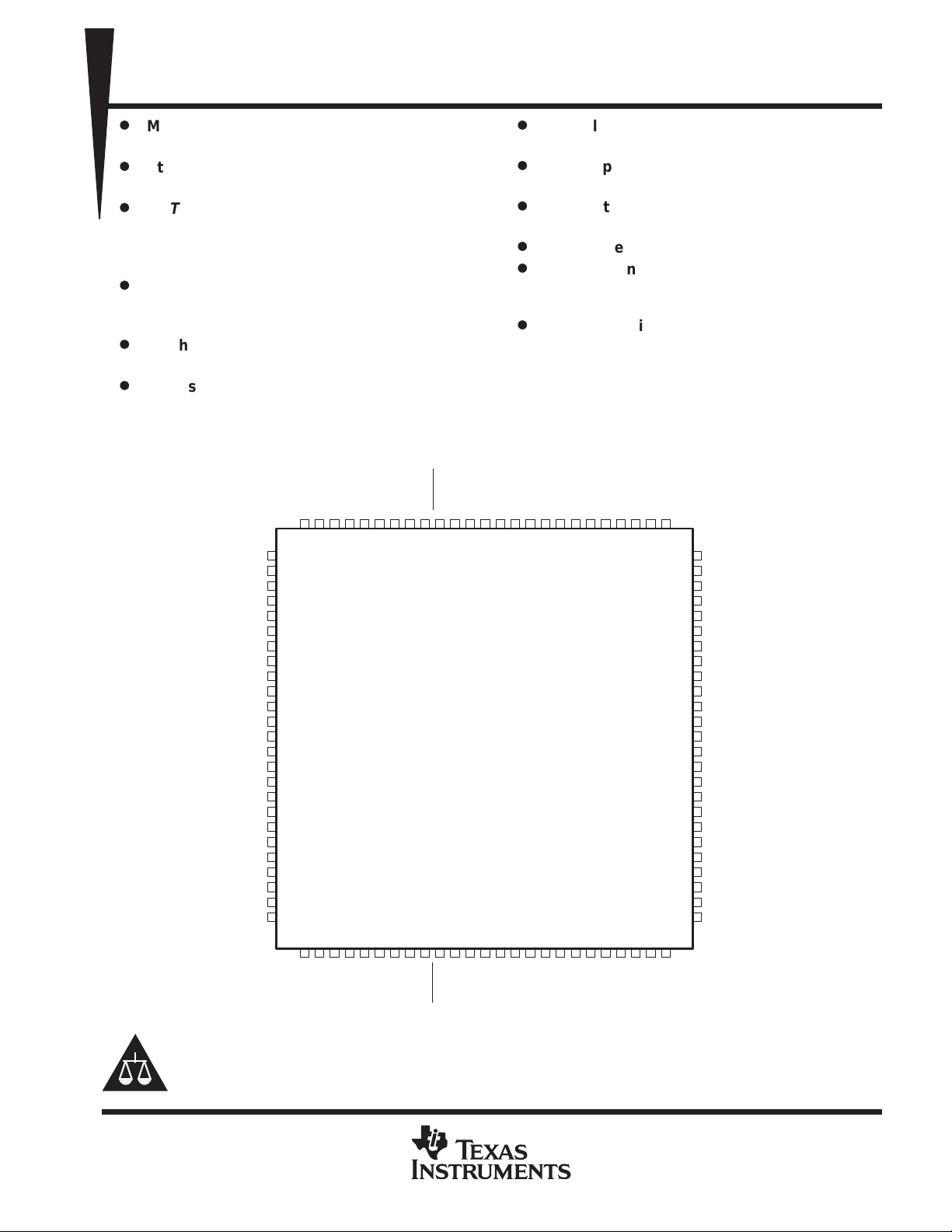
Package Options Include 100-Pin Plastic
Thin Quad Flat (PZ) Package With
14 × 14-mm Body Using 0.5-mm Lead Pitch
and Space-Saving 100-Pin Ceramic Quad
Flat (HS) Package
(Output Ground Bounce)
OLP
†
2A10
2A9
GND
2A8
2A7
2A6
2A5
GND
2A4
2A3
2A2
2A1
V
CC
1A1
1A2
1A3
1A4
GND
1A5
1A6
1A7
1A8
GND
1A9
1A10
1
2
3
4
5
6
7
8
9
10
11
12
13
14
15
16
17
18
19
20
21
22
23
24
25
2A11
2A12
2A13
2A14
GND
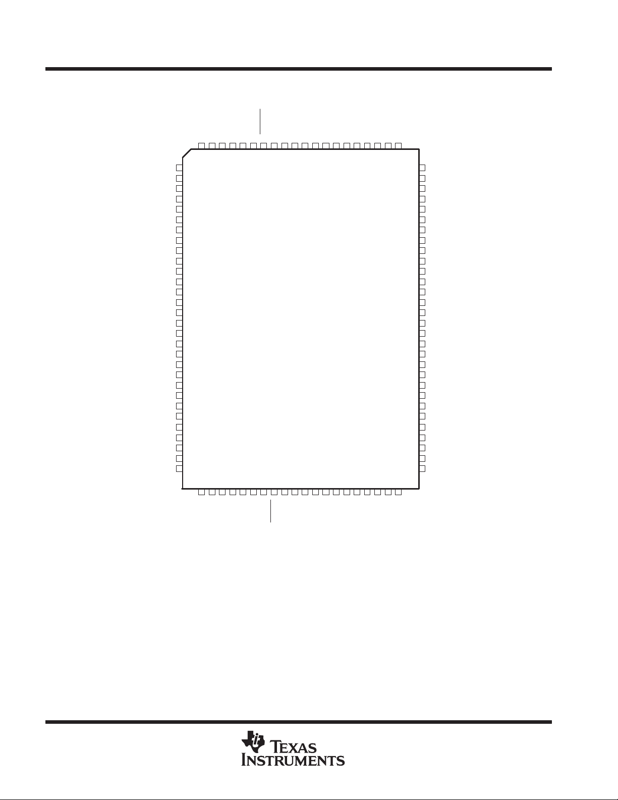
’ABTH32501 ...PZ PACKAGE
2A15
2A16
2A17
2A18
(TOP VIEW)
V
2OEBA
2LEBA
2CLKBA
CC
2CLKAB
2LEAB
2OEAB
2B18
2B17
2B16
2B15
2B14
GND
2B13
2B12
767778798081828384858687888990919293949596979899100
494847464544434241403938373635343332313029282726
50
2B11
2B10
75
2B9
74
GND
73
2B8
72
2B7
71
2B6
70
2B5
69
GND
68
2B4
67
2B3
66
2B2
65
2B1
64
V
63
CC
1B1
62
1B2
61
1B3
60
1B4
59
GND
58
1B5
57
1B6
56
1B7
55
1B8
54
GND
53
1B9
52
1B10
51
GND
1A11
1A12
1A13
1A14
1A15
1A16
1A17
1A18
†
The HS package is not production released.
Please be aware that an important notice concerning availability, standard warranty, and use in critical applications of
Texas Instruments semiconductor products and disclaimers thereto appears at the end of this data sheet.
Widebus+, EPIC-ΙΙB, and UBT are trademarks of Texas Instruments Incorporated.
PRODUCTION DATA information is current as of publication date.
Products conform to specifications per the terms of Texas Instruments
standard warranty. Production processing does not necessarily include
testing of all parameters.
POST OFFICE BOX 655303 • DALLAS, TEXAS 75265
1OEBA
CC
1LEBA
1CLKBAV1CLKAB
1LEAB
1B18
1B17
1OEAB
1B16
1B15
GND
1B14
1B11
1B13
1B12
Copyright 1997, Texas Instruments Incorporated
1
SN54ABTH32501, SN74ABTH32501
36-BIT UNIVERSAL BUS TRANSCEIVERS
WITH 3-STATE OUTPUTS
SCBS229F – JUNE 1992 – REVISED MA Y 1997
2A13
2A12
2A11
2A10
2A9
GND
2A8
2A7
2A6
2A5
GND
2A4
2A3
2A2
2A1
V
CC
1A1
1A2
1A3
1A4
GND
1A5
1A6
1A7
1A8
GND
1A9
1A10
1A11
1A12
1
2
3
4
5
6
7
8
9
10
11
12
13
14
15
16
17
18
19
20
21
22
23
24
25
26
27
28
29
30
SN54ABTH32501 . . . HS PACKAGE
GND
2A14
2A16
2A15
97
98
99
100
34
33
32
31
2A17
2A18
95
96
36
35
(TOP VIEW)
2CLKBA
2LEABA
2OEBA
92
93
94
39
38
37
91
CC
V
40
2OEAB
2LEAB
2CLKAB
88
89
90
43
42
41
2B17
2B18
86
87
45
44
†
2B16
2B15
84
85
47
46
2B14
GND
82
83
49
48
2B13
81
80
79
78
77
76
75
74
73
72
71
70
69
68
67
66
65
64
63
62
61
60
59
58
57
56
55
54
53
52
51
50
2B12
2B11
2B10
2B9
GND
2B8
2B7
2B6
2B5
GND
2B4
2B3
2B2
2B1
V
CC
1B1
1B2
1B3
1B4
GND
1B5
1B6
1B7
1B8
GND
1B9
1B10
1B11
1B12
1B13
CC
GND
1A13
1A14
1A15
1A16
1A17
1A18
1OEBA
†
For HS package availability, please contact the factory or your local TI Field Sales Of fice.
2
POST OFFICE BOX 655303 • DALLAS, TEXAS 75265
V
1LEBA
1CLKBA
1LEAB
1OEAB
1CLKAB
1B18
1B17
1B16
1B15
GND
1B14
SN54ABTH32501, SN74ABTH32501
36-BIT UNIVERSAL BUS TRANSCEIVERS
WITH 3-STATE OUTPUTS
SCBS229F – JUNE 1992 – REVISED MA Y 1997
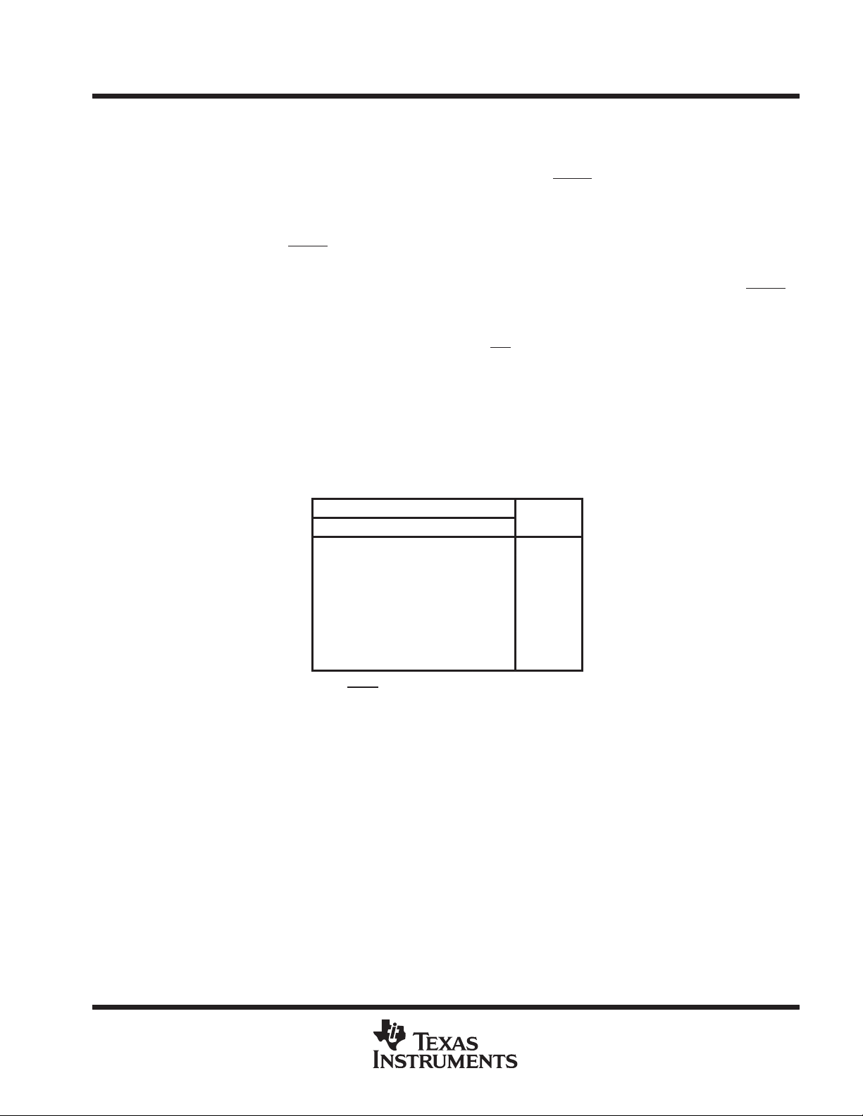
description
These 36-bit UBTs combine D-type latches and D-type flip-flops to allow data flow in transparent, latched, and
clocked modes.
Data flow in each direction is controlled by output-enable (OEAB and OEBA), latch-enable (LEAB and LEBA),
and clock (CLKAB and CLKBA) inputs. For A-to-B data flow, the device operates in the transparent mode when
LEAB is high. When LEAB is low , the A data is latched if CLKAB is held at a high or low logic level. If LEAB is
low, the A data is stored in the latch/flip-flop on the low-to-high transition of CLKAB. Data flow for B to A is similar
to that of A to B, but uses OEBA
Output-enable OEAB is active high. When OEAB is high, the outputs are active. When OEAB is low, the outputs
are in the high-impedance state. The output enables are complementary (OEAB is active high, and OEBA is
active low).
When VCC is between 0 and 2.1 V , the device is in the high-impedance state during power up or power down.
However, to ensure the high-impedance state above 2.1 V, OE should be tied to VCC through a pullup resistor
and OE should be tied to GND through a pulldown resistor; the minimum value of the resistor is determined by
the current-sinking/current-sourcing capability of the driver.
Active bus-hold circuitry is provided to hold unused or floating data inputs at a valid logic level.
The SN54ABTH32501 is characterized for operation over the full military temperature range of –55°C to 125°C.
The SN74ABTH32501 is characterized for operation from –40°C to 85°C.
, LEBA, and CLKBA.
FUNCTION TABLE
INPUTS
OEAB LEAB CLKAB A
L X X X Z
H HXLL
H HXHH
H L ↑ LL
H L ↑ HH
H LHXB
H L L X B
†
A-to-B data flow is shown: B-to-A flow is similar, but
uses OEBA
‡
Output level before the indicated steady-state input
conditions were established
§
Output level before the indicated steady-state input
conditions were established, provided that CLKAB
was low before LEAB went low
, LEBA, and CLKBA.
†
OUTPUT
B
‡
0
§
0
POST OFFICE BOX 655303 • DALLAS, TEXAS 75265
3
 Loading...