

Texas Instruments SN74ABT652DBLE, SN74ABT652DBR, SN74ABT652DW, SN74ABT652DWR, SN74ABT652NT Datasheet
SN54ABT652, SN74ABT652
OCTAL BUS TRANSCEIVERS AND REGISTERS
WITH 3-STATE OUTPUTS
SCBS070D – JULY 1991 – REVISED JULY 1994
Copyright 1994, Texas Instruments Incorporated
2–1
POST OFFICE BOX 655303 • DALLAS, TEXAS 75265
• State-of-the-Art
EPIC-ΙΙB
BiCMOS Design
Significantly Reduces Power Dissipation
• ESD Protection Exceeds 2000 V Per
MIL-STD-883C, Method 3015; Exceeds
200 V Using Machine Model (C = 200 pF,
R = 0)
• Latch-Up Performance Exceeds 500 mA
Per JEDEC Standard JESD-17
• T ypical V
OLP
(Output Ground Bounce)
< 1 V at V
CC
= 5 V, TA = 25°C
• High-Drive Outputs (–32-mA I
OH
,
64-mA IOL)
• Package Options Include Plastic
Small-Outline ((DW)) and Shrink
Small-Outline (DB) Packages, Ceramic
Chip Carriers (FK), and Plastic (NT) and
Ceramic (JT) DIPs
description
These devices consist of bus transceiver circuits,
D-type flip-flops, and control circuitry arranged for
multiplexed transmission of data directly from the
data bus or from the internal storage registers.
Output-enable (OEAB and OEBA
) inputs are
provided to control the transceiver functions.
Select-control (SAB and SBA) inputs are provided
to select whether real-time or stored data is
transferred. The circuitry used for select control
eliminates the typical decoding glitch that occurs
in a multiplexer during the transition between
stored and real-time data. A low input selects
real-time data, and a high input selects stored
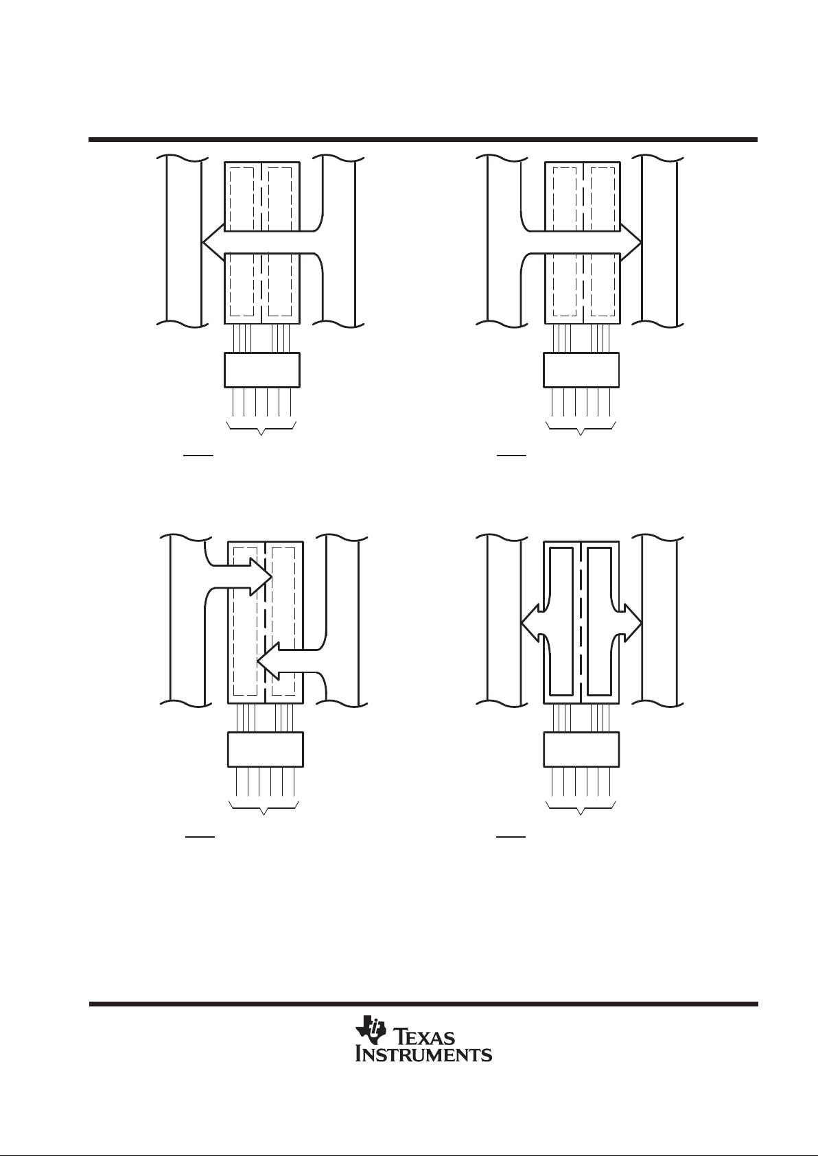
data. Figure 1 illustrates the four fundamental
bus-management functions that can be performed
with the ′ABT652.
Data on the A or B data bus, or both, can be stored in the internal D-type flip-flops by low-to-high transitions at
the appropriate clock (CLKAB or CLKBA) inputs regardless of the select- or enable-control pins. When SAB and
SBA are in the real-time transfer mode, it is possible to store data without using the internal D-type flip-flops by
simultaneously enabling OEAB and OEBA
. In this configuration, each output reinforces its input. When all other
data sources to the two sets of bus lines are at high impedance, each set of bus lines remains at its last state.
To ensure the high-impedance state during power up or power down, OEBA should be tied to VCC through a
pullup resistor; the minimum value of the resistor is determined by the current-sinking capability of the driver
(B to A). OEAB should be tied to GND through a pulldown resistor; the minimum value of the resistor is
determined by the current-sourcing capability of the driver (A to B).
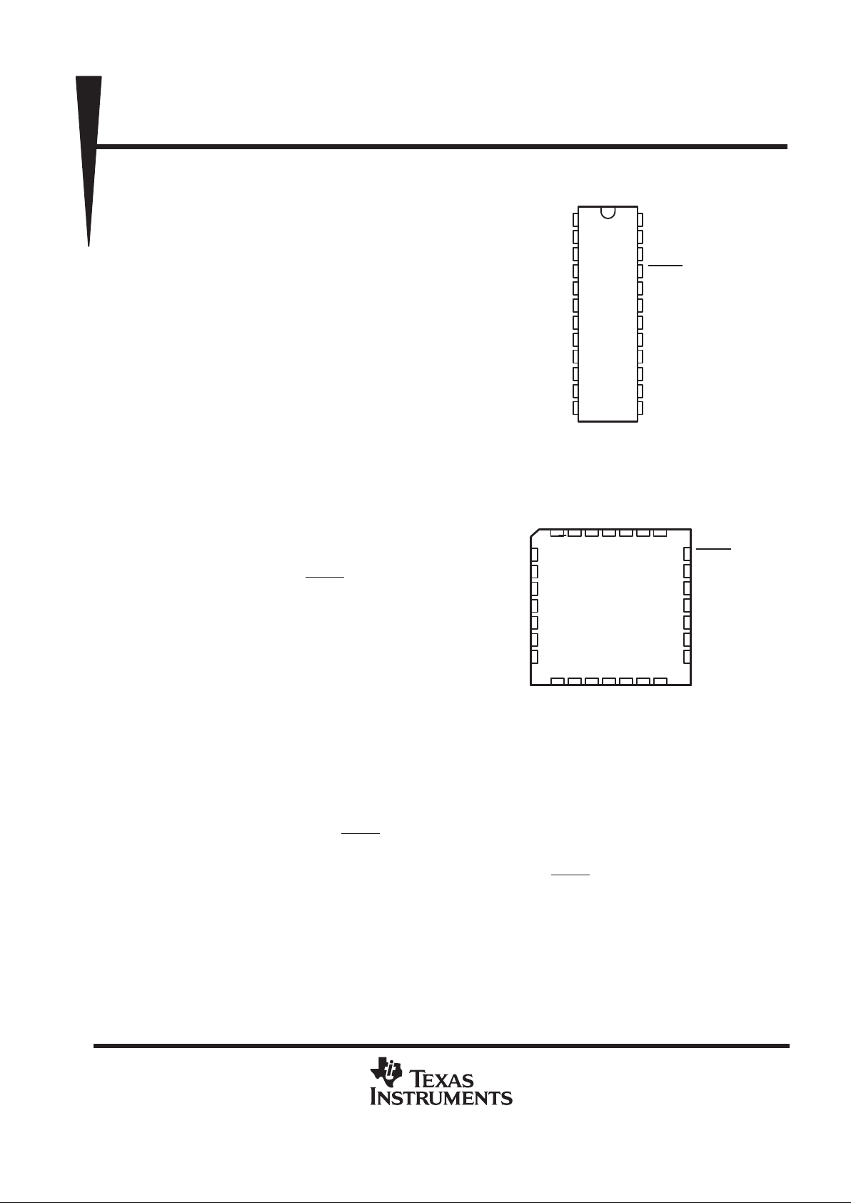
The SN74ABT652 is available in TI’s shrink small-outline package (DB), which provides the same I/O pin count
and functionality of standard small-outline packages in less than half the printed-circuit-board area.
1
2
3
4
5
6
7
8
9
10
11
12
24
23
22
21
20
19
18
17
16
15
14
13
CLKAB
SAB
OEAB
A1
A2
A3
A4
A5
A6
A7
A8
GND
V
CC
CLKBA
SBA
OEBA
B1
B2
B3
B4
B5
B6
B7
B8
SN54ABT652 ...JT PACKAGE
SN74ABT652 ... DB, DW, OR NT PACKAGE
(TOP VIEW)
OEAB
321
13 14
5
6
7
8
9
10
11
OEBA
B1
B2
NC
B3
B4
B5
A1
A2
A3
NC
A4
A5
A6
4
15 16 17 18
A8
GND
NC
B8B7B6
SAB
CLKAB
NC
SN54ABT652 . . . FK PACKAGE
(TOP VIEW)
28 27 26
25
24
23
22
21
20
19
12
A7
V
CLKBA
SBA
NC – No internal connection
CC
EPIC-ΙΙB is a trademark of Texas Instruments Incorporated.
UNLESS OTHERWISE NOTED this document contains PRODUCTION
DATA information current as of publication date. Products conform to
specifications per the terms of Texas Instruments standard warranty.
Production processing does not necessarily include testing of all
parameters.

SN54ABT652, SN74ABT652
OCTAL BUS TRANSCEIVERS AND REGISTERS
WITH 3-STATE OUTPUTS
SCBS070D – JULY 1991 – REVISED JULY 1994
2–2
POST OFFICE BOX 655303 • DALLAS, TEXAS 75265
description (continued)
The SN54ABT652 is characterized for operation over the full military temperature range of –55°C to 125°C. The
SN74ABT652 is characterized for operation from –40°C to 85°C.
FUNCTION TABLE
INPUTS
DATA I/O
†
OEAB OEBA CLKAB CLKBA SAB SBA A1 THRU A8 B1 THRU B8
OPERATION OR FUNCTION
L H H or L H or L X X Input Input Isolation
L H ↑↑X X Input Input Store A and B data
X H ↑ H or L X X Input Unspecified
‡
Store A, hold B
H H ↑↑X
‡
X Input Output Store A in both registers
L X H or L ↑ X X Unspecified
‡
Input Hold A, store B
L L ↑↑XX‡Output Input Store B in both registers
L L X X X L Output Input Real-time B data to A bus
L L X H or L X H Output Input Stored B data to A bus
H H X X L X Input Output Real-time A data to B bus
H H H or L X H X Input Output Stored A data to B bus
H L H or L H or L H H Output Output
Stored A data to B bus and
stored B data to A bus
†
The data output functions may be enabled or disabled by a variety of level combinations at the OEAB or OEBA inputs. Data input functions are
always enabled; i.e., data at the bus pins is stored on every low-to-high transition on the clock inputs.
‡
Select control = L; clocks can occur simultaneously.
Select control = H; clocks must be staggered in order to load both registers.
SN54ABT652, SN74ABT652
OCTAL BUS TRANSCEIVERS AND REGISTERS
WITH 3-STATE OUTPUTS
SCBS070D – JULY 1991 – REVISED JULY 1994
2–3
POST OFFICE BOX 655303 • DALLAS, TEXAS 75265
BUS B
BUS A
BUS B
BUS A
BUS B
BUS A
BUS B
BUS A
OEAB
3
X
L
L
OEAB
3
L
21
L
1
CLKAB
X
23
CLKBA
X
2
SAB
X
22
SBA
L
1
CLKAB
X
23
CLKBA
X
2
SAB
L
22
SBA
X
21
H
1
CLKAB23CLKBA
X
2
SAB
X
22
SBA
X
1
CLKAB23CLKBA2SAB22SBA
X
H
XX
X
X
X
HL L HH
↑
↑
↑↑
OEBA
OEBA
3
H
21
H
OEAB OEBA
321
OEAB OEBA
L
REAL-TIME TRANSFER
BUS B TO BUS A
REAL-TIME TRANSFER
BUS A TO BUS B
STORAGE FROM
A, B, OR A AND B
TRANSFER STORED DATA
TO A AND/OR B
Figure 1. Bus-Management Functions
Pin numbers shown are for the DB, DW, JT, and NT packages.
SN54ABT652, SN74ABT652
OCTAL BUS TRANSCEIVERS AND REGISTERS
WITH 3-STATE OUTPUTS
SCBS070D – JULY 1991 – REVISED JULY 1994
2–4
POST OFFICE BOX 655303 • DALLAS, TEXAS 75265
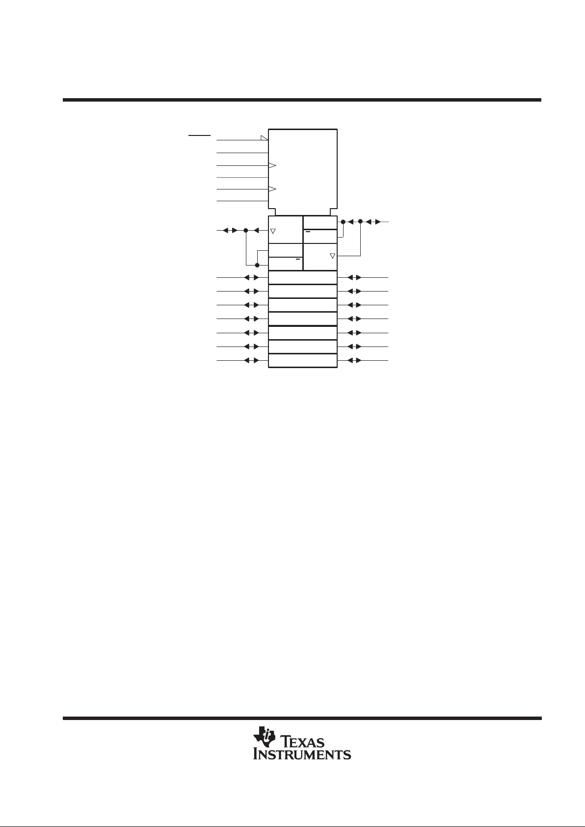
logic symbol
†
OEBA
EN1 [BA]
21
G5
22
SBA
A1
4
B1
20
4D
EN2 [AB]
3
OEAB
23
CLKBA
1
CLKAB
G7
2
SAB
5
7
7
5
1
1
6D ≥1
≥1
1
2
C6
C4
A2
5
B2
19
A3
6
B3
18
A4
7
B4
17
A5
8
B5
16
A6
9
B6
15
A7
10
B7
14
A8
11
B8
13
†
This symbol is in accordance with ANSI/IEEE Std 91-1984 and IEC Publication 617-12.
Pin numbers shown are for the DB, DW, JT, and NT packages.
 Loading...