

Texas Instruments SN74ABT652ADW, SN74ABT652ADWR, SN74ABT652ANT, SN74ABT652ADBLE, SN74ABT652ADBR Datasheet
...
SN54ABT652A, SN74ABT652A
OCTAL REGISTERED TRANSCEIVERS
WITH 3-STATE OUTPUTS
SCBS072F – JANUARY 1991 – REVISED MA Y 1997
D
State-of-the-Art
EPIC-ΙΙB
BiCMOS Design
Significantly Reduces Power Dissipation
D
ESD Protection Exceeds 2000 V Per
MIL-STD-883, Method 3015; Exceeds 200 V
Using Machine Model (C = 200 pF, R = 0)
D
Latch-Up Performance Exceeds 500 mA Per
JEDEC Standard JESD-17
D
Typical V
(Output Ground Bounce)
OLP
< 1 V at VCC = 5 V, TA = 25°C
D
High-Drive Outputs (–32-mA IOH, 64-mA IOL)
D
Package Options Include Plastic
Small-Outline (DW), Shrink Small-Outline
(DB), and Thin Shrink Small-Outline (PW)
Packages, Ceramic Chip Carriers (FK),
Ceramic Flat (W) Package, and Plastic (NT)
and Ceramic (JT) DIPs
description
These devices consist of bus-transceiver circuits,
D-type flip-flops, and control circuitry arranged for
multiplexed transmission of data directly from the
data bus or from the internal storage registers.
Output-enable (OEAB and OEBA) inputs are
provided to control the transceiver functions.
Select-control (SAB and SBA) inputs are provided
to select either real-time or stored data for
transfer. The circuitry used for select control
eliminates the typical decoding glitch that occurs
in a multiplexer during the transition between
stored and real-time data. A low input selects
real-time data, and a high input selects stored
data. Figure 1 illustrates the four fundamental
bus-management functions that can be
performed with the ’ABT652A.
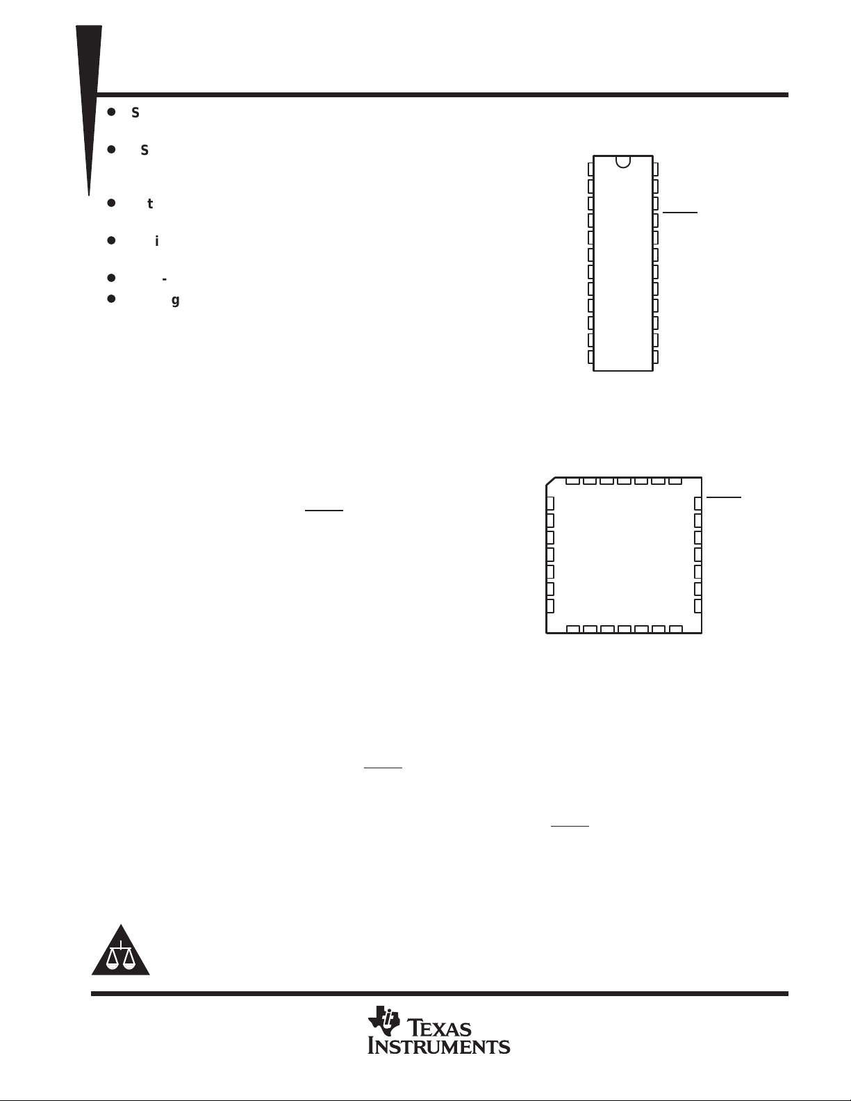
SN54ABT652A . . . JT OR W PACKAGE
SN74ABT652A . . . DB, DW, NT, OR PW PACKAGE
CLKAB
SN54ABT652A . . . FK PACKAGE
A1
A2
A2
NC
A4
A5
A6
NC – No internal connection
(TOP VIEW)
24
23
22
21
20
19
18
17
16
15
14
13
CC
V
B8B7B6
NC
V
CC
CLKBA
SBA
OEBA
B1
B2
B3
B4
B5
B6
B7
B8
SBA
25
24
23
22
21
20
19
OEBA
B1
B2
NC
B3
B4
B5
1
SAB
2
OEAB
GND
3
A1
4
A2
5
A3
6
A4
7
A5
8
A6
9
A7
10
A8
11
12
(TOP VIEW)
OEAB
SAB
CLKABNCCLKBA
3212827
426
5
6
7
8
9
10
11
12 13
14 15 16 17 18
A7
A8
GND
Data on the A- or B-data bus, or both, can be stored in the internal D-type flip-flops by low-to-high transitions
at the appropriate clock (CLKAB or CLKBA) inputs, regardless of the select- or enable-control inputs. When SAB
and SBA are in the real-time transfer mode, it is possible to store data without using the internal D-type flip-flops
by simultaneously enabling OEAB and OEBA
. In this configuration, each output reinforces its input. When all
other data sources to the two sets of bus lines are at high impedance, each set of bus lines remains at its last
state.
To ensure the high-impedance state during power up or power down, OEBA should be tied to VCC through a
pullup resistor; the minimum value of the resistor is determined by the current-sinking capability of the driver
(B to A). OEAB should be tied to GND through a pulldown resistor; the minimum value of the resistor is
determined by the current-sourcing capability of the driver (A to B).
Please be aware that an important notice concerning availability, standard warranty, and use in critical applications of
Texas Instruments semiconductor products and disclaimers thereto appears at the end of this data sheet.
EPIC-ΙΙB is a trademark of Texas Instruments Incorporated.
PRODUCTION DATA information is current as of publication date.
Products conform to specifications per the terms of Texas Instruments
standard warranty. Production processing does not necessarily include
testing of all parameters.
POST OFFICE BOX 655303 • DALLAS, TEXAS 75265
Copyright 1997, Texas Instruments Incorporated
1
SN54ABT652A, SN74ABT652A
OPERATION OR FUNCTION
OCTAL REGISTERED TRANSCEIVERS
WITH 3-STATE OUTPUTS
SCBS072F – JANUARY 1991 – REVISED MA Y 1997
description (continued)
The SN54ABT652A is characterized for operation over the full military temperature range of –55°C to 125°C.
The SN74ABT652A is characterized for operation from –40°C to 85°C.
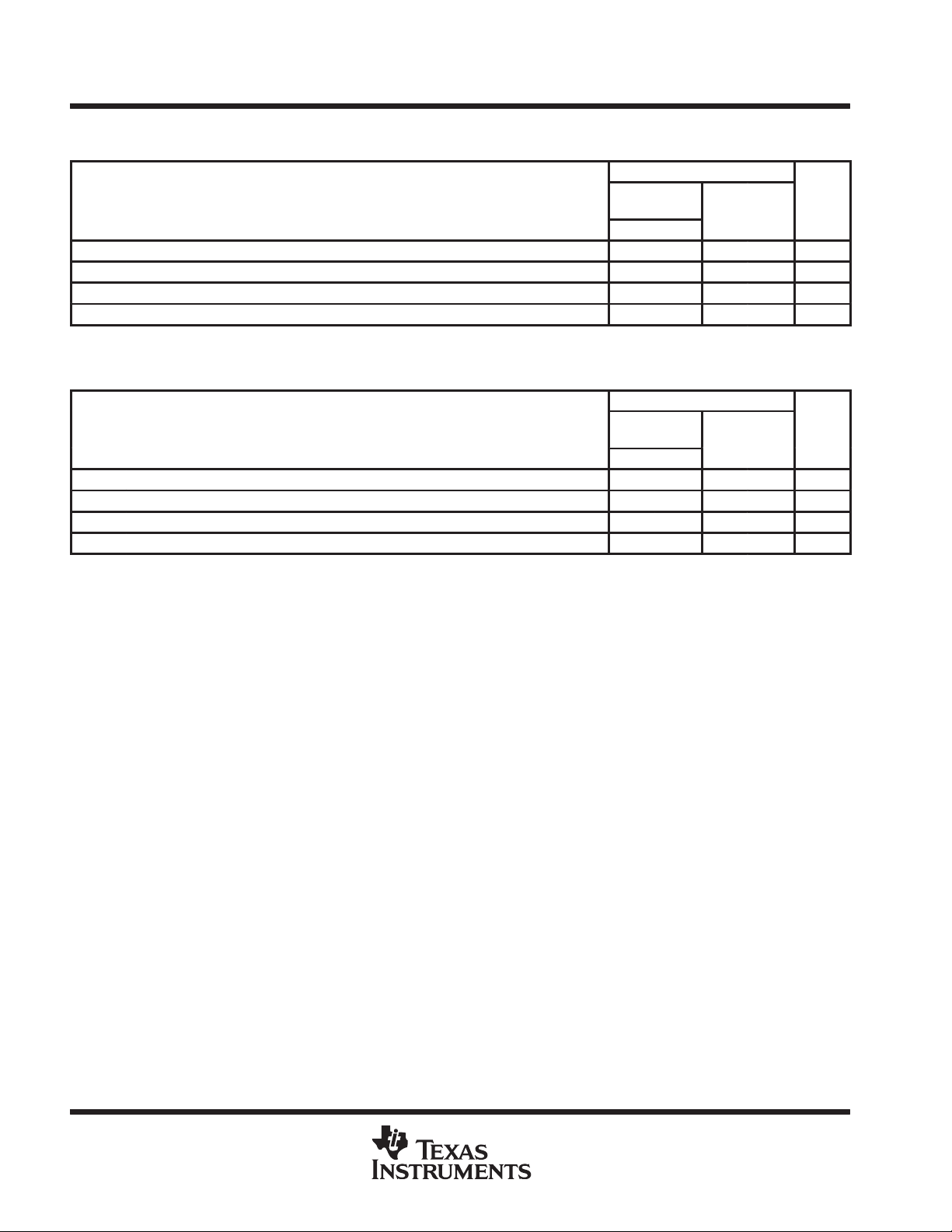
FUNCTION TABLE
INPUTS
OEAB OEBA CLKAB CLKBA SAB SBA A1–A8 B1–B8
L H H or L H or L X X Input Input Isolation
L H ↑↑X X Input Input Store A and B data
X H ↑ H or L X X Input Unspecified
H H ↑↑X
L X H or L ↑ X X Unspecified
L L ↑↑XX‡Output Input Store B in both registers
L L X X X L Output Input Real-time B data to A bus
L L X H or L X H Output Input Stored B data to A bus
H H X X L X Input Output Real-time A data to B bus
H H H or L X H X Input Output Stored A data to B bus
H L H or L H or L H H Output Output
†
The data-output functions may be enabled or disabled by a variety of level combinations at OEAB or OEBA
enabled; i.e., data at the bus terminals is stored on every low-to-high transition of the clock inputs.
‡
Select control = L; clocks can occur simultaneously.
Select control = H; clocks must be staggered to load both registers.
‡
X Input Output Store A in both registers
DATA I/O
†
‡
‡
Input Hold A, store B
Store A, hold B
Stored A data to B bus and
stored B data to A bus
. Data-input functions are always
2
POST OFFICE BOX 655303 • DALLAS, TEXAS 75265
SN54ABT652A, SN74ABT652A
OCTAL REGISTERED TRANSCEIVERS
WITH 3-STATE OUTPUTS
SCBS072F – JANUARY 1991 – REVISED MA Y 1997
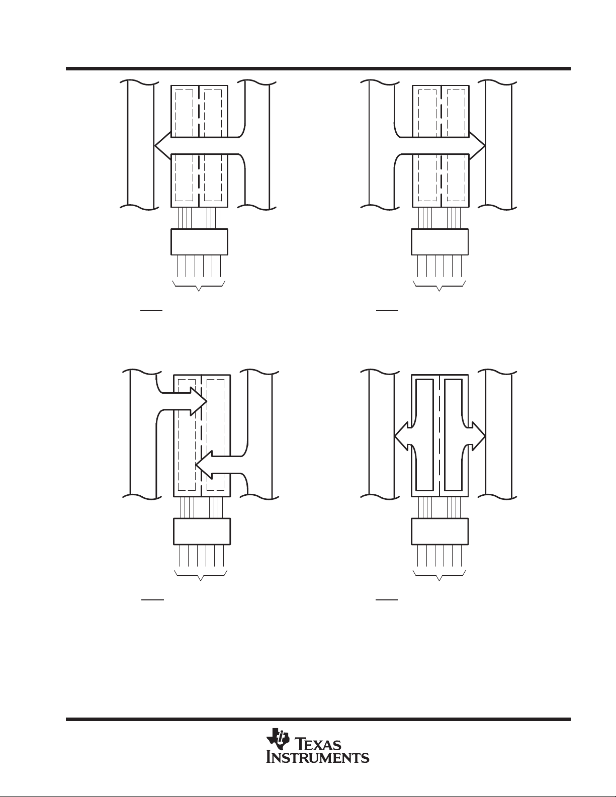
BUS A
3 21 1 23 2 22 1 23 2 22321
OEAB
OEBA
LL
CLKABXCLKBAXSABXSBA
REAL-TIME TRANSFER
BUS B TO BUS A
BUS A
BUS B
OEAB OEBA
L
BUS B
BUS A
HH
BUS A
BUS B
CLKABXCLKBAXSABLSBA
X
REAL-TIME TRANSFER
BUS A TO BUS B
BUS B
3 21 23 2 22 3 21 1 2 22
OEAB
Pin numbers shown are for the DB, DW, JT, NT, PW, and W packages.
OEBA
X
L
L
H
X
H
1
CLKAB CLKBAXSABXSBA
↑
XX
↑
X
↑↑
STORAGE FROM
A, B, OR A AND B
X
X
X
Figure 1. Bus-Management Functions
POST OFFICE BOX 655303 • DALLAS, TEXAS 75265
23
OEAB OEBA
H L H or L H H
CLKAB CLKBA SAB SBA
H or L
TRANSFER STORED DA TA
TO A AND/OR B
3
SN54ABT652A, SN74ABT652A
OCTAL REGISTERED TRANSCEIVERS
WITH 3-STATE OUTPUTS
SCBS072F – JANUARY 1991 – REVISED MA Y 1997
logic symbol
†
This symbol is in accordance with ANSI/IEEE Std 91-1984 and IEC Publication 617-12.
Pin numbers shown are for the DB, DW, JT, NT, PW, and W packages.
†
SBA
SAB
A1
A2
A3
A4
A5
A6
A7
A8
21
3
23
22
1
2
4
5
6
7
8
9
10
11
EN1 [BA]
EN2 [AB]
C4
G5
C6
G7
5
≥1
1
5
7
6D ≥1
1
7
4D
1
2
OEBA
OEAB
CLKBA
CLKAB
19
18
17
16
15
14
13
20
B1
B2
B3
B4
B5
B6
B7
B8
4
POST OFFICE BOX 655303 • DALLAS, TEXAS 75265

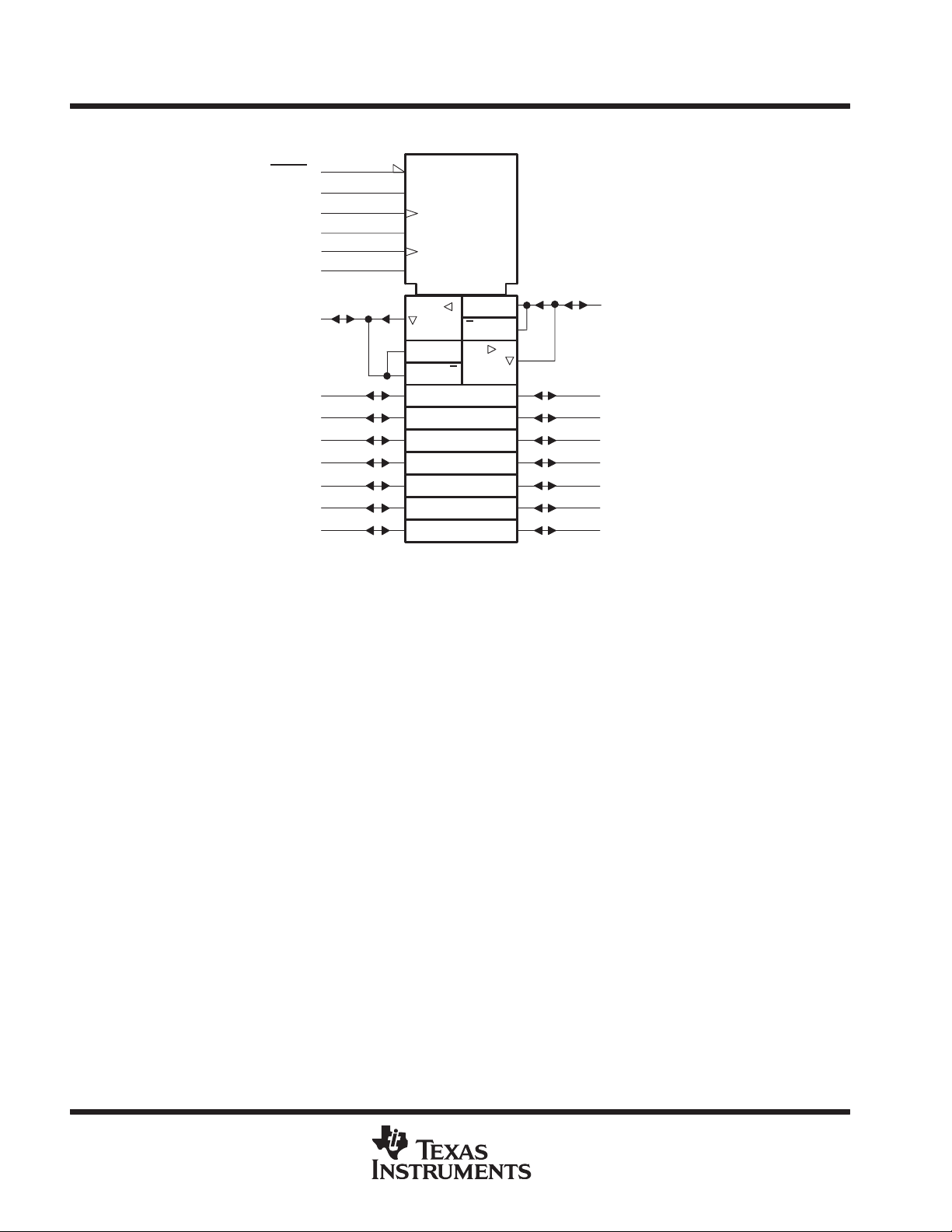
logic diagram (positive logic)
SN54ABT652A, SN74ABT652A
OCTAL REGISTERED TRANSCEIVERS
WITH 3-STATE OUTPUTS
SCBS072F – JANUARY 1991 – REVISED MA Y 1997
OEBA
OEAB
CLKBA
SBA
CLKAB
SAB
A1
21
3
23
22
1
2
4
One of Eight Channels
1D
C1
C1
1D
20
B1
To Seven Other Channels
Pin numbers shown are for the DB, DW, JT, NT, PW, and W packages.
POST OFFICE BOX 655303 • DALLAS, TEXAS 75265
5

SN54ABT652A, SN74ABT652A
UNIT
OCTAL REGISTERED TRANSCEIVERS
WITH 3-STATE OUTPUTS
SCBS072F – JANUARY 1991 – REVISED MA Y 1997
absolute maximum ratings over operating free-air temperature range (unless otherwise noted)
Supply voltage range, V
Input voltage range, VI (except I/O ports) (see Note 1) –0.5 V to 7 V. . . . . . . . . . . . . . . . . . . . . . . . . . . . . . . . . .
Voltage range applied to any output in the high or power-off state, VO –0.5 V to 5.5 V. . . . . . . . . . . . . . . . . . .
Current into any output in the low state, IO: SN54ABT652A 96 mA. . . . . . . . . . . . . . . . . . . . . . . . . . . . . . . . . . .
Input clamp current, I
Output clamp current, I
Package thermal impedance, θ
Storage temperature range, T
†
Stresses beyond those listed under “absolute maximum ratings” may cause permanent damage to the device. These are stress ratings only, and
functional operation of the device at these or any other conditions beyond those indicated under “recommended operating conditions” is not
implied. Exposure to absolute-maximum-rated conditions for extended periods may affect device reliability.
NOTES: 1. The input and output negative-voltage ratings may be exceeded if the input and output clamp-current ratings are observed.
2. The package thermal impedance is calculated in accordance with EIA/JEDEC Std JESD51, except for through-hole packages,
which use a trace length of zero.
–0.5 V to 7 V. . . . . . . . . . . . . . . . . . . . . . . . . . . . . . . . . . . . . . . . . . . . . . . . . . . . . . . . . .
CC
SN74ABT652A 128 mA. . . . . . . . . . . . . . . . . . . . . . . . . . . . . . . . . . .
(V
< 0) –18 mA. . . . . . . . . . . . . . . . . . . . . . . . . . . . . . . . . . . . . . . . . . . . . . . . . . . . . . . . . . .
IK
I
(V
OK
< 0) –50 mA. . . . . . . . . . . . . . . . . . . . . . . . . . . . . . . . . . . . . . . . . . . . . . . . . . . . . . . .
O
(see Note 2): DB package 104°C/W. . . . . . . . . . . . . . . . . . . . . . . . . . . . . . . .
JA
DW package 81°C/W. . . . . . . . . . . . . . . . . . . . . . . . . . . . . . . . .
NT package 67°C/W. . . . . . . . . . . . . . . . . . . . . . . . . . . . . . . . .
PW package 120°C/W. . . . . . . . . . . . . . . . . . . . . . . . . . . . . . . .
–65°C to 150°C. . . . . . . . . . . . . . . . . . . . . . . . . . . . . . . . . . . . . . . . . . . . . . . . . . .
stg
recommended operating conditions (see Note 3)
SN54ABT652A SN74ABT652A
MIN MAX MIN MAX
V
V
V
V
I
OH
I
OL
∆t/∆v Input transition rise or fall rate Outputs enabled 5 5 ns/V
T
NOTE 3: Unused pins (input or I/O) must be held high or low to prevent them from floating.
Supply voltage 4.5 5.5 4.5 5.5 V
CC
High-level input voltage 2 2 V
IH
Low-level input voltage 0.8 0.8 V
IL
Input voltage 0 V
I
High-level output current –24 –32 mA
Low-level output current 48 64 mA
Operating free-air temperature –55 125 –40 85 °C
A
CC
0 V
CC
V
†
6
POST OFFICE BOX 655303 • DALLAS, TEXAS 75265

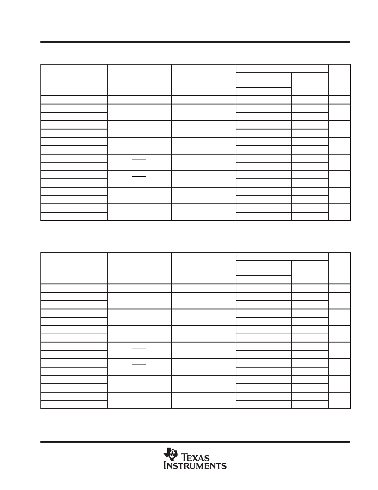
PARAMETER
TEST CONDITIONS
UNIT
V
V
V
4.5 V
VOLV
V
V
I
V
V
V
GND
A
V
CC
SN54ABT652A, SN74ABT652A
OCTAL REGISTERED TRANSCEIVERS
WITH 3-STATE OUTPUTS
SCBS072F – JANUARY 1991 – REVISED MA Y 1997
electrical characteristics over recommended operating free-air temperature range (unless
otherwise noted)
TA = 25°C SN54ABT652A SN74ABT652A
MIN TYP†MAX MIN MAX MIN MAX
V
IK
OH
V
hys
I
I
OZH
I
OZL
I
off
I
CEX
I
O
I
CC
∆I
C
C
* On products compliant to MIL-PRF-38535, this parameter does not apply.
** These limits apply only to the SN74ABT652A.
†
All typical values are at VCC = 5 V.
‡
The parameters I
§
Not more than one output should be tested at a time, and the duration of the test should not exceed one second.
¶
This is the increase in supply current for each input that is at the specified TTL voltage level rather than VCC or GND.
Control inputs
A or B ports
‡
‡
§
¶
CC
Control inputs VI = 2.5 V or 0.5 V 7 pF
i
A or B ports VO = 2.5 V or 0.5 V 12 pF
io
OZH
VCC = 4.5 V, II = –18 mA –1.2 –1.2 –1.2 V
VCC = 4.5 V, IOH = –3 mA 2.5 2.5 2.5
VCC = 5 V, IOH = –3 mA 3 3 3
=
CC
= 4.5
CC
= 5.5 V,
CC
VCC = 5.5 V, VO = 2.7 V 50** 10 50 µA
VCC = 5.5 V, VO = 0.5 V –50** –10 –50 µA
VCC = 0, VI or VO ≤ 4.5 V ±100 ±100 µA
VCC = 5.5 V,
VO = 5.5 V
VCC = 5.5 V, VO = 2.5 V –50 –100 –180 –50 –180 –50 –180 mA
=
= 5.5 V,
IO = 0,
VI = VCC or GND
VCC = 5.5 V, One input at 3.4 V,
Other inputs at VCC or GND
and I
include the input leakage current.
OZL
IOH = –24 mA 2 2
IOH = –32 mA 2* 2
IOL = 48 mA 0.55 0.55
IOL = 64 mA 0.55* 0.55
100 mV
=
or
I
CC
Outputs high 50 50 50 µA
Outputs high 250 250 250 µA
Outputs low 30 30 30 mA
Outputs disabled 250 250 250 µA
±1 ±1 ±1
±100 ±100 ±100
1.5 1.5 1.5 mA
µ
POST OFFICE BOX 655303 • DALLAS, TEXAS 75265
7
SN54ABT652A, SN74ABT652A
OCTAL REGISTERED TRANSCEIVERS
WITH 3-STATE OUTPUTS
SCBS072F – JANUARY 1991 – REVISED MA Y 1997
timing requirements over recommended ranges of supply voltage and operating free-air
temperature (unless otherwise noted) (see Figure 2)
SN54ABT652A
VCC = 5 V,
f
clock
t
w
t
su
t
h
TA = 25°C
MIN MAX
Clock frequency 0 125 0 125 MHz
Pulse duration, CLK high or low 4 4 ns
Setup time, A or B before CLKAB↑ or CLKBA↑ 3 3.5 ns
Hold time, A or B after CLKAB↑ or CLKBA↑ 1.5 1.5 ns
MIN MAX
timing requirements over recommended ranges of supply voltage and operating free-air
temperature (unless otherwise noted) (see Figure 2)
SN74ABT652A
VCC = 5 V,
f
clock
t
w
t
su
t
h
TA = 25°C
MIN MAX
Clock frequency 0 125 0 125 MHz
Pulse duration, CLK high or low 4 4 ns
Setup time, A or B before CLKAB↑ or CLKBA↑ 3 3 ns
Hold time, A or B after CLKAB↑ or CLKBA↑ 0 0 ns
MIN MAX
UNIT
UNIT
8
POST OFFICE BOX 655303 • DALLAS, TEXAS 75265
CLK
B or A
ns
A or B
B or A
ns
SAB
SBA
†
B or A
ns
OEBA
A
ns
OEBA
A
ns
OEAB
B
ns
OEAB
B
ns
CLK
B or A
ns
A or B
B or A
ns
SAB
SBA
†
B or A
ns
OEBA
A
ns
OEBA
A
ns
OEAB
B
ns
OEAB
B
ns
SN54ABT652A, SN74ABT652A
OCTAL REGISTERED TRANSCEIVERS
WITH 3-STATE OUTPUTS
SCBS072F – JANUARY 1991 – REVISED MA Y 1997
switching characteristics over recommended ranges of supply voltage and operating free-air
temperature, C
PARAMETER
f
max
t
PLH
t
PHL
t
PLH
t
PHL
t
PLH
t
PHL
t
PZH
t
PZL
t
PHZ
t
PLZ
t
PZH
t
PZL
t
PHZ
t
†
These parameters are measured with the internal output state of the storage register opposite that of the bus input.
PLZ
= 50 pF (unless otherwise noted) (see Figure 2)
L
FROM
(INPUT)
or
TO
(OUTPUT)
SN54ABT652A
VCC = 5 V,
TA = 25°C
MIN TYP MAX
125 200 125 MHz
2.2 4 5.1 1.7 5.9
1.7 4 5.1 1.7 5.9
1.5 3 4.8 1 5
1.5 3.3 4.6 1 5.6
1.5 4 5.5 1.5 6.8
1.5 3.6 4.9 1.5 6.2
2 3.6 5.4 2 6.8
3 5.7 7.7 3 9.2
1.5 3.2 5.8 1 7.5
1.5 3 4.3 1 4.6
2 4.3 6.1 2 7.8
3 5.5 7.4 3 8.9
1.5 3.3 6 1 8
1.5 3.4 5 1.5 6.8
MIN MAX
UNIT
switching characteristics over recommended ranges of supply voltage and operating free-air
temperature, C
PARAMETER
f
max
t
PLH
t
PHL
t
PLH
t
PHL
t
PLH
t
PHL
t
PZH
t
PZL
t
PHZ
t
PLZ
t
PZH
t
PZL
t
PHZ
t
†
These parameters are measured with the internal output state of the storage register opposite that of the bus input.
PLZ
= 50 pF (unless otherwise noted) (see Figure 2)
L
FROM
(INPUT)
or
TO
(OUTPUT)
SN74ABT652A
VCC = 5 V,
TA = 25°C
MIN TYP MAX
125 200 125 MHz
2.2 4 5.1 2.2 5.6
1.7 4 5.1 1.7 5.6
1.5 3 4.3 1.5 4.8
1.5 3.3 4.6 1.5 5.4
1.5 4 5.1 1.5 6.5
1.5 3.6 4.9 1.5 5.9
2 3.6 4.6 2 5.8
3 5.7 6.8 3 8.5
1.5 3.2 4.5 1.5 5
1.5 3 3.8 1.5 4.1
2 4.3 6.1 2 6.5
3 5.5 6.5 3 7.4
1.5 3.3 4.5 1.5 5.5
1.5 3.4 4.4 1.5 5.1
MIN MAX
UNIT
POST OFFICE BOX 655303 • DALLAS, TEXAS 75265
9
SN54ABT652A, SN74ABT652A
OCTAL REGISTERED TRANSCEIVERS
WITH 3-STATE OUTPUTS
SCBS072F – JANUARY 1991 – REVISED MA Y 1997
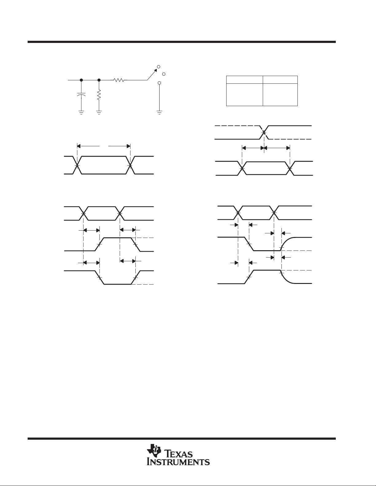
PARAMETER MEASUREMENT INFORMATION
From Output
Under Test
CL = 50 pF
(see Note A)
500 Ω
500 Ω
S1
7 V
GND
Open
TEST S1
t
PLH/tPHL
t
PLZ/tPZL
t
PHZ/tPZH
Open
7 V
Open
LOAD CIRCUIT
t
w
Input
Input
Output
Output
INVERTING AND NONINVERTING OUTPUTS
1.5 V 1.5 V
VOLTAGE WAVEFORMS
PULSE DURATION
1.5 V 1.5 V
t
PLH
1.5 V
t
PHL
VOLTAGE WAVEFORMS
PROPAGATION DELAY TIMES
t
PHL
1.5 V
t
1.5 V1.5 V
PLH
3 V
0 V
3 V
0 V
V
V
V
V
OH
OL
OH
OL
Timing Input
Data Input
Output
Control
Output
Waveform 1
S1 at 7 V
(see Note B)
Output
Waveform 2
S1 at Open
(see Note B)
1.5 V
t
su
1.5 V 1.5 V
VOLTAGE WAVEFORMS
SETUP AND HOLD TIMES
1.5 V
t
PZL
t
PLZ
1.5 V
t
t
PZH
ENABLE AND DISABLE TIMES
LOW- AND HIGH-LEVEL ENABLING
PHZ
1.5 V
VOLTAGE WAVEFORMS
t
h
1.5 V
VOL + 0.3 V
VOH – 0.3 V
3 V
0 V
3 V
0 V
3 V
0 V
3.5 V
V
OL
V
OH
≈ 0 V
NOTES: A. CL includes probe and jig capacitance.
B. Waveform 1 is for an output with internal conditions such that the output is low except when disabled by the output control.
Waveform 2 is for an output with internal conditions such that the output is high except when disabled by the output control.
C. All input pulses are supplied by generators having the following characteristics: PRR ≤ 10 MHz, ZO = 50 Ω, tr ≤ 2.5 ns, tf≤ 2.5 ns.
D. The outputs are measured one at a time with one transition per measurement.
Figure 2. Load Circuit and Voltage Waveforms
10
POST OFFICE BOX 655303 • DALLAS, TEXAS 75265

IMPORTANT NOTICE
T exas Instruments and its subsidiaries (TI) reserve the right to make changes to their products or to discontinue
any product or service without notice, and advise customers to obtain the latest version of relevant information
to verify, before placing orders, that information being relied on is current and complete. All products are sold
subject to the terms and conditions of sale supplied at the time of order acknowledgement, including those
pertaining to warranty, patent infringement, and limitation of liability.
TI warrants performance of its semiconductor products to the specifications applicable at the time of sale in
accordance with TI’s standard warranty. Testing and other quality control techniques are utilized to the extent
TI deems necessary to support this warranty . Specific testing of all parameters of each device is not necessarily
performed, except those mandated by government requirements.
CERTAIN APPLICA TIONS USING SEMICONDUCT OR PRODUCTS MAY INVOLVE POTENTIAL RISKS OF
DEATH, PERSONAL INJURY, OR SEVERE PROPERTY OR ENVIRONMENTAL DAMAGE (“CRITICAL
APPLICATIONS”). TI SEMICONDUCTOR PRODUCTS ARE NOT DESIGNED, AUTHORIZED, OR
WARRANTED TO BE SUITABLE FOR USE IN LIFE-SUPPORT DEVICES OR SYSTEMS OR OTHER
CRITICAL APPLICA TIONS. INCLUSION OF TI PRODUCTS IN SUCH APPLICATIONS IS UNDERST OOD TO
BE FULLY AT THE CUSTOMER’S RISK.
In order to minimize risks associated with the customer’s applications, adequate design and operating
safeguards must be provided by the customer to minimize inherent or procedural hazards.
TI assumes no liability for applications assistance or customer product design. TI does not warrant or represent
that any license, either express or implied, is granted under any patent right, copyright, mask work right, or other
intellectual property right of TI covering or relating to any combination, machine, or process in which such
semiconductor products or services might be or are used. TI’s publication of information regarding any third
party’s products or services does not constitute TI’s approval, warranty or endorsement thereof.
Copyright 1998, Texas Instruments Incorporated
 Loading...