

Texas Instruments SN74ABT373DBLE, SN74ABT373DBR, SN74ABT373DW, SN74ABT373DWR, SN74ABT373N Datasheet
...
SN54ABT373, SN74ABT373
OCTAL TRANSPARENT D-TYPE LATCHES
WITH 3-STATE OUTPUTS
SCBS155D – JANUARY 1991 – REVISED MA Y 1997
1
POST OFFICE BOX 655303 • DALLAS, TEXAS 75265
D
State-of-the-Art
EPIC-ΙΙB
BiCMOS Design
Significantly Reduces Power Dissipation
D
Latch-Up Performance Exceeds 500 mA Per
JEDEC Standard JESD-17
D
T ypical V
OLP
(Output Ground Bounce) < 1 V
at VCC = 5 V, TA = 25°C
D
High-Drive Outputs (–32-mA IOH, 64-mA IOL)
D
Package Options Include Plastic
Small-Outline (DW), Shrink Small-Outline
(DB), and Thin Shrink Small-Outline (PW)
Packages, Ceramic Chip Carriers (FK),
Ceramic Flat (W) Package, and Plastic (N)
and Ceramic (J) DIPs
description
The eight latches of the ’ABT373 are transparent
D-type latches. While the latch-enable (LE) input
is high, the Q outputs follow the data (D) inputs.
When LE is taken low, the Q outputs are latched
at the logic levels set up at the D inputs.
A buffered output-enable (OE
) input can be used
to place the eight outputs in either a normal logic
state (high or low logic levels) or a
high-impedance state. In the high-impedance
state, the outputs neither load nor drive the bus
lines significantly . The high-impedance state and
increased drive provide the capability to drive bus
lines without need for interface or pullup
components.
OE
does not affect the internal operations of the latches. Old data can be retained or new data can be entered
while the outputs are in the high-impedance state.
T o ensure the high-impedance state during power up or power down, OE should be tied to VCC through a pullup
resistor; the minimum value of the resistor is determined by the current-sinking capability of the driver.
The SN54ABT373 is characterized for operation over the full military temperature range of –55°C to 125°C. The
SN74ABT373 is characterized for operation from –40°C to 85°C.
FUNCTION TABLE
(each latch)
INPUTS
OUTPUT
OE LE D
Q
L H H H
L HL L
L LX Q
0
H X X Z
Copyright 1997, Texas Instruments Incorporated
PRODUCTION DATA information is current as of publication date.
Products conform to specifications per the terms of Texas Instruments
standard warranty. Production processing does not necessarily include
testing of all parameters.
Please be aware that an important notice concerning availability, standard warranty, and use in critical applications of
Texas Instruments semiconductor products and disclaimers thereto appears at the end of this data sheet.
EPIC-ΙΙB is a trademark of Texas Instruments Incorporated.
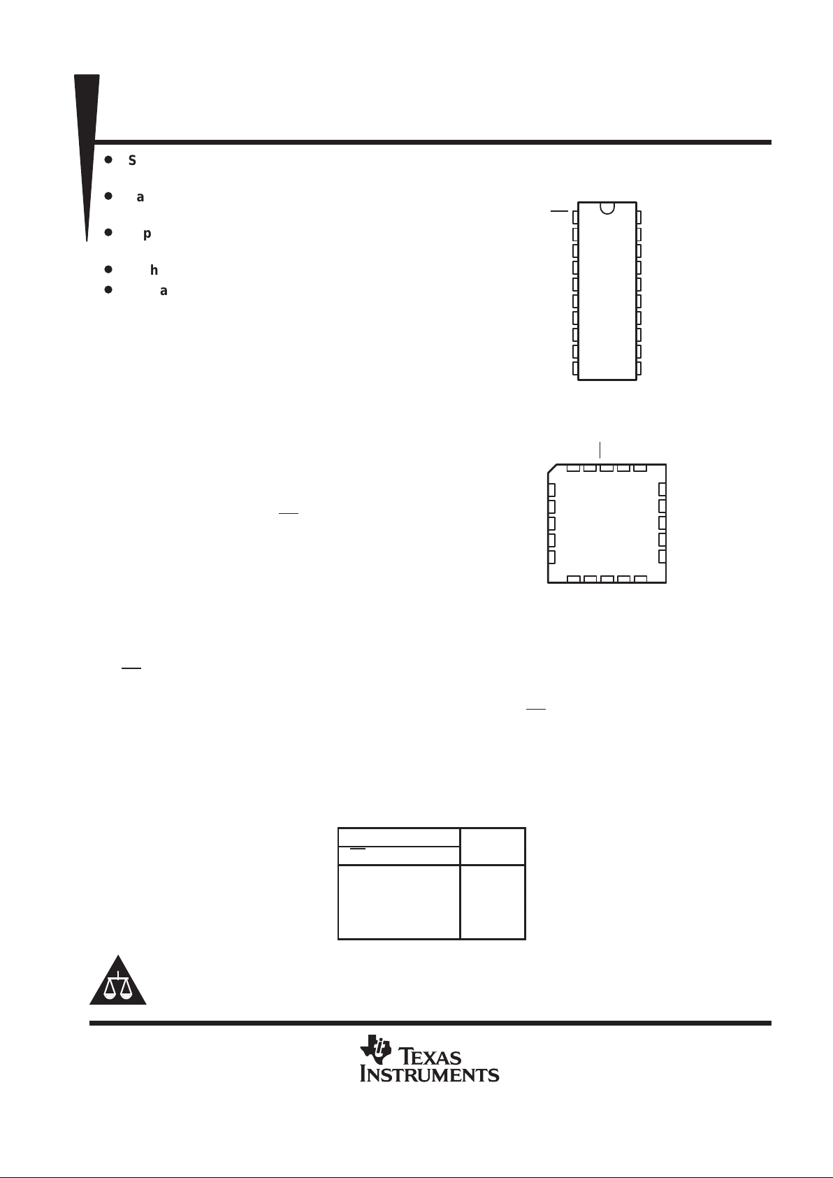
SN54ABT373 ...J OR W PACKAGE
SN74ABT373 . . . DB, DW, N, OR PW PACKAGE
(TOP VIEW)
SN54ABT373 . . . FK PACKAGE
(TOP VIEW)
1
2
3
4
5
6
7
8
9
10
20
19
18
17
16
15
14
13
12
11
OE
1Q
1D
2D
2Q
3Q
3D
4D
4Q
GND
V
CC
8Q
8D
7D
7Q
6Q
6D
5D
5Q
LE
3 2 1 20 19
9 10 11 12 13
4
5
6
7
8
18
17
16
15
14
2D
2Q
3Q
3D
4D
1D1QOE
5Q
5D
8Q
4Q
GND
LE
V
CC
8D
7D
7Q
6Q
6D
SN54ABT373, SN74ABT373
OCTAL TRANSPARENT D-TYPE LATCHES
WITH 3-STATE OUTPUTS
SCBS155D – JANUARY 1991 – REVISED MA Y 1997
2
POST OFFICE BOX 655303 • DALLAS, TEXAS 75265
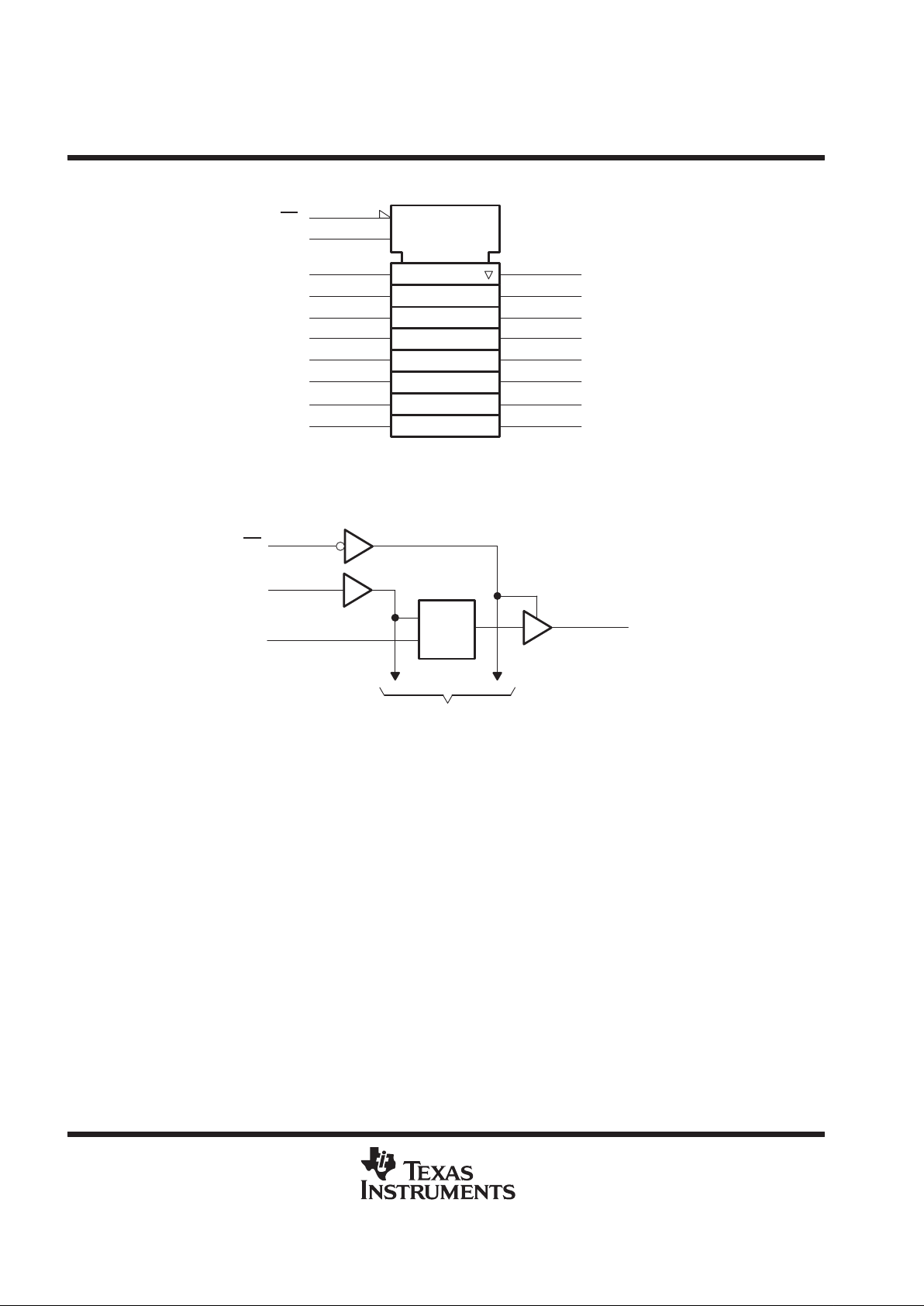
logic symbol
†
1D
3
1D
4
2D
7
3D
EN
1
1Q
2
2Q
5
3Q
6
8
4D
13
5D
14
6D
4Q
9
5Q
12
6Q
15
OE
17
7D
18
8D
C1
11
LE
7Q
16
8Q
19
†
This symbol is in accordance with ANSI/IEEE Std 91-1984 and IEC Publication 617-12.
logic diagram (positive logic)
OE
To Seven Other Channels
1
11
3
2
LE
1D
C1
1D
1Q
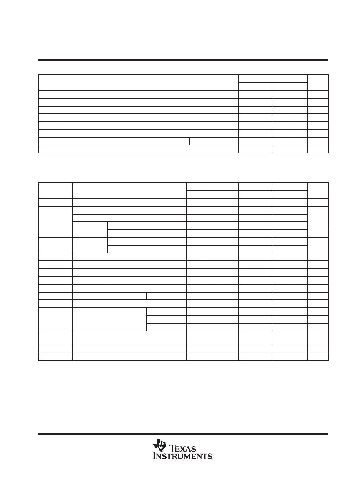
absolute maximum ratings over operating free-air temperature range (unless otherwise noted)
‡
Supply voltage range, VCC –0.5 V to 7 V. . . . . . . . . . . . . . . . . . . . . . . . . . . . . . . . . . . . . . . . . . . . . . . . . . . . . . . . . .
Input voltage range, V
I
(see Note 1) –0.5 V to 7 V. . . . . . . . . . . . . . . . . . . . . . . . . . . . . . . . . . . . . . . . . . . . . . . . . .
Voltage range applied to any output in the high or power-off state, VO –0.5 V to 5.5 V. . . . . . . . . . . . . . . . . . .
Current into any output in the low state, IO: SN54ABT373 96 mA. . . . . . . . . . . . . . . . . . . . . . . . . . . . . . . . . . . .
SN74ABT373 128 mA. . . . . . . . . . . . . . . . . . . . . . . . . . . . . . . . . . .
Input clamp current, IIK (VI < 0) –18 mA. . . . . . . . . . . . . . . . . . . . . . . . . . . . . . . . . . . . . . . . . . . . . . . . . . . . . . . . . . .
Output clamp current, I
OK
(VO < 0) –50 mA. . . . . . . . . . . . . . . . . . . . . . . . . . . . . . . . . . . . . . . . . . . . . . . . . . . . . . . .
Package thermal impedance, θ
JA
(see Note 2): DB package 115°C/W. . . . . . . . . . . . . . . . . . . . . . . . . . . . . . . .
DW package 97°C/W. . . . . . . . . . . . . . . . . . . . . . . . . . . . . . . . .
N package 67°C/W. . . . . . . . . . . . . . . . . . . . . . . . . . . . . . . . . . .
PW package 128°C/W. . . . . . . . . . . . . . . . . . . . . . . . . . . . . . . .
Storage temperature range, T
stg
–65°C to 150°C. . . . . . . . . . . . . . . . . . . . . . . . . . . . . . . . . . . . . . . . . . . . . . . . . . .
‡
Stresses beyond those listed under “absolute maximum ratings” may cause permanent damage to the device. These are stress ratings only, and
functional operation of the device at these or any other conditions beyond those indicated under “recommended operating conditions” is not
implied. Exposure to absolute-maximum-rated conditions for extended periods may affect device reliability.
NOTES: 1. The input and output negative-voltage ratings may be exceeded if the input and output clamp-current ratings are observed.
2. The package thermal impedance is calculated in accordance with EIA/JEDEC Std JESD51, except for through-hole packages,
which use a trace length of zero.
SN54ABT373, SN74ABT373
OCTAL TRANSPARENT D-TYPE LATCHES
WITH 3-STATE OUTPUTS
SCBS155D – JANUARY 1991 – REVISED MA Y 1997
3
POST OFFICE BOX 655303 • DALLAS, TEXAS 75265
recommended operating conditions (see Note 3)
SN54ABT373 SN74ABT373
MIN MAX MIN MAX
UNIT
V
CC
Supply voltage 4.5 5.5 4.5 5.5 V
V
IH
High-level input voltage 2 2 V
V
IL
Low-level input voltage 0.8 0.8 V
V
I
Input voltage 0 V
CC
0 V
CC
V
I
OH
High-level output current –24 –32 mA
I
OL
Low-level output current 48 64 mA
∆t/∆v Input transition rise or fall rate Outputs enabled 5 5 ns/V
T
A
Operating free-air temperature –55 125 –40 85 °C
NOTE 3: Unused inputs must be held high or low to prevent them from floating.
electrical characteristics over recommended operating free-air temperature range (unless
otherwise noted)
TA = 25°C SN54ABT373 SN74ABT373
PARAMETER
TEST CONDITIONS
MIN TYP†MAX MIN MAX MIN MAX
UNIT
V
IK
VCC = 4.5 V, II = –18 mA –1.2 –1.2 –1.2 V
VCC = 4.5 V, IOH = –3 mA
2.5 2.5 2.5
VCC = 5 V, IOH = –3 mA
3 3 3
V
OH
IOH = –24 mA
2 2
V
V
CC
= 4.5
V
IOH = –32 mA
2* 2
IOL = 48 mA
0.55 0.55
V
OL
V
CC
=
4.5 V
IOL = 64 mA
0.55* 0.55
V
V
hys
100 mV
I
I
VCC = 5.5 V, VI = VCC or GND ±1 ±1 ±1 µA
I
OZH
VCC = 5.5 V, VO = 2.7 V 10
‡
10
‡
10
‡
µA
I
OZL
VCC = 5.5 V, VO = 0.5 V –10
‡
–10
‡
–10
‡
µA
I
off
VCC = 0, VI or VO ≤ 4.5 V ±100 ±100 µA
I
CEX
VCC = 5.5 V, VO = 5.5 V Outputs high 50 50 50 µA
I
O
§
VCC = 5.5 V, VO = 2.5 V –50 –100 –180 –50 –180 –50 –180 mA
Outputs high
1 250 250 250
µA
I
CC
VCC = 5.5 V, IO = 0,
Outputs low
24 30 30 30
mA
V
I
=
V
CC
or
GND
Outputs disabled
0.5 250 250 250
µA
∆I
CC
¶
VCC = 5.5 V , One input at 3.4 V,
Other inputs at VCC or GND
1.5 1.5 1.5 mA
C
i
VI = 2.5 V or 0.5 V 3 pF
C
o
VO = 2.5 V or 0.5 V 6 pF
* On products compliant to MIL-PRF-38535, this parameter does not apply.
†
All typical values are at VCC = 5 V.
‡
This data sheet limit may vary among suppliers.
§
Not more than one output should be tested at a time, and the duration of the test should not exceed one second.
¶
This is the increase in supply current for each input that is at the specified TTL voltage level rather than VCC or GND.
 Loading...