

Texas Instruments SN65LVDS9637AD, SN65LVDS9637ADR, SN65LVDT32AD, SN65LVDT32ADR, SN65LVDT3486AD Datasheet
...
SN65LVDS32A, SN65LVDT32A, SN65LVDS3486A
SN65LVDT3486A, SN65LVDS9637A, SN65LVDT9637A
HIGH-SPEED DIFFERENTIAL RECEIVERS
SLLS368C – JULY 1999 – REVISED JANUAR Y 2000
1
POST OFFICE BOX 655303 • DALLAS, TEXAS 75265
D
Meets or Exceeds the Requirements of
ANSI EIA/TIA-644 Standard for Signaling
Rates† Up to 400 Mbps
D
Operates With a Single 3.3 V Supply
D
–2 V to 4.4 V Common-Mode Input Voltage
Range
D
Differential Input Thresholds <50 mV With
50 mV of Hysteresis Over Entire
Common-Mode Input Voltage Range
D
Integrated 110Ω Line Termination Resistors
Offered With the LVDT Series
D
Propagation Delay Times 4 ns (typ)
D
Open-Circuit and Terminated Fail Safe
Assures a High-Level Output With No Input
D
Bus-Pin ESD Protection Exceeds 15 kV
HBM
D
Outputs High-Impedance With VCC < 1.5 V
D
Power Dissipation <400 mW With Four
Receivers Switching at 200 MHz
D
Available in Small-Outline Package With
1,27 mm T erminal Pitch
D
Pin-Compatible With the AM26LS32,
MC3486, or uA9637
description
This family of differential line receivers offer
improved performance and features that implement the electrical characteristics of low-voltage
differential signaling (LVDS). LVDS is defined in
the TIA/EIA-644 standard. This improved performance represents the second generation of
receiver products for this standard providing a
better overall solution for the cabled environment.
The next generation family of products is an
extension to TI’s overall product portfolio and is
not necessarily a replacement for older LVDS
receivers.
Improved features include an input commonmode voltage range 2 V wider than the minimum
required by the standard. This will allow longer
cable lengths by tripling the allowable ground
noise tolerance to 3 V between a driver and
receiver.
Copyright 2000, Texas Instruments Incorporated
Please be aware that an important notice concerning availability, standard warranty, and use in critical applications of
Texas Instruments semiconductor products and disclaimers thereto appears at the end of this data sheet.
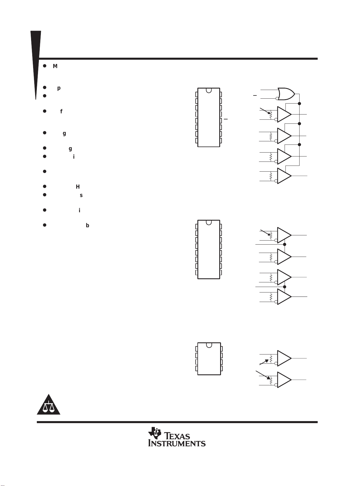
1
2
3
4
5
6
7
8
16
15
14
13
12
11
10
9
1B
1A
1Y
G
2Y
2A
2B
GND
V
CC
4B
4A
4Y
G
3Y
3A
3B
SN65LVDT32A
1
2
3
4
8
7
6
5
V
CC
1Y
2Y
GND
1A
1B
2A
2B
D PACKAGE
(TOP VIEW)
D PACKAGE
(TOP VIEW)
SN65LVDS32A
G
G
1A
1B
2A
2B
3A
3B
4A
4B
1Y
2Y
3Y
4Y
Logic Diagram
(positive logic)
SN65LVDT32A
ONLY (4 Places)
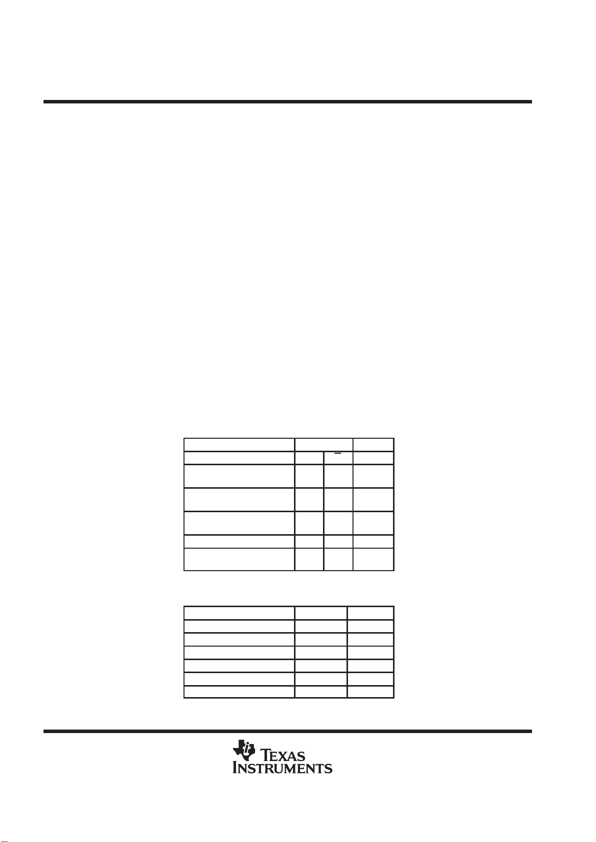
1
2
3
4
5
6
7
8
16
15
14
13
12
11
10
9
1B
1A
1Y
1,2EN
2Y
2A
2B
GND
V
CC
4B
4A
4Y
3,4EN
3Y
3A
3B
SN65LVDT3486A
D PACKAGE
(TOP VIEW)
SN65LVDS3486A
1A
1B
2A
2B
3A
3B
4A
4B
1Y
2Y
3Y
4Y
Logic Diagram
(positive logic)
SN65LVDT3486A
ONLY (4 Places)
1,2EN
3,4EN
1A
1B
2A
2B
1Y
2Y
SN65LVDT9637A
ONLY
SN65LVDT9637A
SN65LVDS9637A
Logic Diagram
(positive logic)
PRODUCTION DATA information is current as of publication date.
Products conform to specifications per the terms of Texas Instruments
standard warranty. Production processing does not necessarily include
testing of all parameters.
†
Signaling rate, 1/t, where t is the minimum unit interval and is expressed in the units bits/s (bits per second)
SN65LVDS32A, SN65LVDT32A, SN65LVDS3486A
SN65LVDT3486A, SN65LVDS9637A, SN65LVDT9637A
HIGH-SPEED DIFFERENTIAL RECEIVERS
SLLS368C – JULY 1999 – REVISED JANUAR Y 2000
2
POST OFFICE BOX 655303 • DALLAS, TEXAS 75265
description (continued)
Precise control of the differential input voltage thresholds now allows for inclusion of 50 mV of input voltage
hysteresis to improve noise rejection on slowly changing input signals. The input thresholds are still no more
than ±50 mV over the full input common-mode voltage range. See
Application Information
for more details on
this feature.
The high-speed switching of L VDS signals almost always necessitates the use of a line impedance matching
resistor at the receiving-end of the cable or transmission media. The SN65L VDT series of receivers eliminates
this external resistor by integrating it with the receiver. The nonterminated SN65LVDS series is also available
for multidrop or other termination circuits.
The receivers can withstand ±15 kV human-body model (HBM) and ±600 V machine model (MM) electrostatic
discharges to the receiver input pins with respect to ground without damage. This provides reliability in cabled
and other connections where potentially damaging noise is always a threat.
The receivers also include a (patent pending) fail-safe circuit that will provide a high-level output within 500 ns
after loss of the input signal. The most common causes of signal loss are disconnected cables, shorted lines,
or powered-down transmitters. This prevents noise from being received as valid data under these fault
conditions. This feature may also be used for wired-OR bus signaling.
The intended application of these devices and signaling technique is for point-to-point baseband data
transmission over controlled impedance media of approximately 100 Ω. The transmission media may be
printed-circuit board traces, backplanes, or cables. The ultimate rate and distance of data transfer is dependent
upon the attenuation characteristics of the media and the noise coupling to the environment.
The SN65LVDS32A, SN65LVDT32A, SN65LVDS3486A, SN65LVDT3486A, SN65LVDS9637A, and
SN65LVDT9637A are characterized for operation from -40°C to 85°C.
Function Tables
SN65LVDS32A and SN65LVDT32A
DIFFERENTIAL INPUT
ENABLES OUTPUT
A-B G G Y
VID ≥ -70 mV
H
X
X
L
H
H
-100 mV < VID ≤ -70 mV
H
X
X
L
?
?
VID≤ -100 mV
H
X
X
L
L
L
X L H Z
Open
H
X
X
L
H
H
H = high level, L = low level, X = irrelevant,
Z = high impedance (off), ? = indeterminate
SN65LVDS3486A and SN65LVDT3486A
DIFFERENTIAL INPUT
ENABLES OUTPUT
A-B EN Y
VID ≥ -70 mV H H
-100 mV < VID ≤ -70 mV H ?
VID≤ -100 mV H L
X L Z
Open H H
H = high level, L = low level, X = irrelevant,
Z = high impedance (off), ? = indeterminate
SN65LVDS32A, SN65LVDT32A, SN65LVDS3486A
SN65LVDT3486A, SN65LVDS9637A, SN65LVDT9637A
HIGH-SPEED DIFFERENTIAL RECEIVERS
SLLS368C – JULY 1999 – REVISED JANUAR Y 2000
3
POST OFFICE BOX 655303 • DALLAS, TEXAS 75265
Function Tables (Continued)
SN65LVDS9637A and SN65LVDT9637A
DIFFERENTIAL INPUT
OUTPUT
A-B Y
VID ≥ -70 mV H
-100 mV < VID ≤ -70 mV ?
VID≤ -100 mV L
Open H
H = high level, L = low level, ? = indeterminate
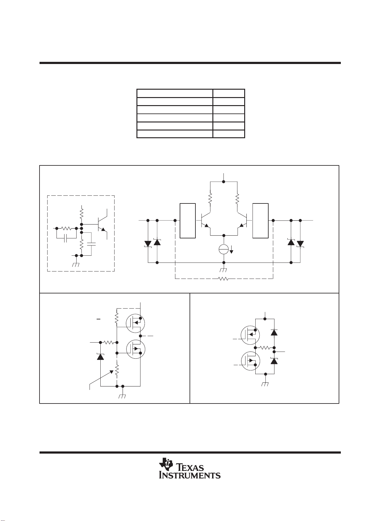
equivalent input and output schematic diagrams
V
CC
37 Ω
7 V
Y Output
LVDT Only 110 Ω
7 V
300 kΩ
50 Ω
V
CC
Enable
Inputs
300 kΩ
(G
Only)
(EN and G Only)
7 V
V
CC
Attenuation
Network
18 V
A Input
Attenuation
Network
B Input
18 V7 V
V
CC
Attenuation
Network
SN65LVDS32A, SN65LVDT32A, SN65LVDS3486A
SN65LVDT3486A, SN65LVDS9637A, SN65LVDT9637A
HIGH-SPEED DIFFERENTIAL RECEIVERS
SLLS368C – JULY 1999 – REVISED JANUAR Y 2000
4
POST OFFICE BOX 655303 • DALLAS, TEXAS 75265
absolute maximum ratings over operating free-air temperature (unless otherwise noted)
†
Supply voltage range, VCC (see Note 1) –0.5 V to 4 V. . . . . . . . . . . . . . . . . . . . . . . . . . . . . . . . . . . . . . . . . . . . . .
Voltage range: Enables or Y –0.5 V to VCC + 3 V. . . . . . . . . . . . . . . . . . . . . . . . . . . . . . . . . . . . . . . . . . . . . . . . . .
A or B –4 V to 6 V. . . . . . . . . . . . . . . . . . . . . . . . . . . . . . . . . . . . . . . . . . . . . . . . . . . . . . . . . . . . . . . .
Electrostatic discharge: A, B, and GND (see Note 2) Class 3, A: 15 kV, B: 600 V. . . . . . . . . . . . . . . . . . . . . . .
All pins Class 3, A: 7 kV, B: 500 V. . . . . . . . . . . . . . . . . . . . . . . . . . . . . . . . . . . . . . . . . .
Continuous power dissipation See Dissipation Rating Table. . . . . . . . . . . . . . . . . . . . . . . . . . . . . . . . . . . . . . . . .
Storage Temperature range –65°C to 150°C. . . . . . . . . . . . . . . . . . . . . . . . . . . . . . . . . . . . . . . . . . . . . . . . . . . . . . .
Lead temperature 1,6 mm (1/16 inch) from case for 10 seconds 260°C. . . . . . . . . . . . . . . . . . . . . . . . . . . . . . .
†
Stresses beyond those listed under “absolute maximum ratings” may cause permanent damage to the device. These are stress ratings only, and
functional operation of the device at these or any other conditions beyond those indicated under “recommended operating conditions” is not
implied. Exposure to absolute-maximum-rated conditions for extended periods may affect device reliability.
NOTES: 1. All voltage values, except differential I/O bus voltages, are with respect to network ground terminal.
2. Tested in accordance with MIL-STD-883C Method 3015.7.
DISSIPATION RATING T ABLE
PACKAGE
TA ≤ 25°C
POWER RATING
OPERATING FACTOR
‡
ABOVE TA = 25°C
TA = 85°C
POWER RATING
D8 725 mW 5.8 mW/°C 377 mW
D16 950 mW 7.6 mW/°C 494 mW
‡
This is the inverse of the junction-to-ambient thermal resistance when board-mounted and with
no air flow.
recommended operating conditions
MIN NOM MAX UNIT
Supply voltage, V
CC
3 3.3 3.6 V
High-level input voltage, V
IH
Enables 2 V
Low-level input voltage, V
IL
Enables 0.8 V
Magnitude of differential input voltage, VID 0.1 3 V
Common-mode input voltage, V
IC
–2 4.4 V
Operating free-air temperature, T
A
–40 85 °C
SN65LVDS32A, SN65LVDT32A, SN65LVDS3486A
SN65LVDT3486A, SN65LVDS9637A, SN65LVDT9637A
HIGH-SPEED DIFFERENTIAL RECEIVERS
SLLS368C – JULY 1999 – REVISED JANUAR Y 2000
5
POST OFFICE BOX 655303 • DALLAS, TEXAS 75265
electrical characteristics over recommended operating conditions (unless otherwise noted)
PARAMETER TEST CONDITIONS MIN TYP†MAX UNIT
V
ITH1
Positive-going differential input voltage threshold
50
V
ITH2
Negative-going differential input voltage threshold
V
IB
=-2 V or 4.4 V,
See Figure 1
–50
mV
V
ITH3
Differential input fail-safe voltage threshold See Figure 2 and Table 1 –70 –100 mV
V
ID(HYS)
Differential input voltage hysteresis,
V
ITH1
- V
ITH2
50 mV
V
OH
High-level output voltage IOH = –8 mA 2.4 V
V
OL
Low-level output voltage IOL = 8 mA 0.4 V
‘32A or ‘3486A
G or EN at VCC, No load,
Steady-state
16 23
I
CC
Supply current
G or EN at GND 1.1 5
mA
‘9637A No load, Steady-state 8 12
VI = 0 V, Other input open ±20
VI =2.4 V , Other input open ±20
SN65LVDS
VI =-2 V, Other input open ±40
µ
A
p
p
VI = 4.4 V, Other input open ±40
IIInput current (A or B inputs)
VI = 0 V, Other input open ±40
VI =2.4 V , Other input open ±40
SN65LVDT
VI =-2 V, Other input open ±80
µ
A
VI = 4.4 V, Other input open ±80
Differential input current
SN65LVDS
VID= 100 mV , VIC= –2 V or 4.4 V,
See Figure 1
±2 µA
I
ID
Differential in ut current
(IIA - IIB)
VID= 0.4 V , VIC= –2 V or 4.4 V 3.1 4.5 mA
SN65LVDT
VID= –0.4 V , VIC= –2 V or 4.4 V –3.1 –4.5 mA
p
p
VA or VB =0 or 2.4 V,
VCC= 0 V
±30
I
I(OFF)
Power-off input current (A or B inputs)
VA or VB =–2 V or 4.4 V,
VCC= 0 V
±50
µ
A
I
IH
High-level input current (enables) VIH = 2 V 10 µA
I
IL
Low-level input current (enables) VIL = 0.8 V 10 µA
I
OZ
High-impedance output current ±10 µA
C
IN
Input capacitance, A or B input to GND VI = 0.4 sin (4E6πt) + 0.5 V 5 pF
†
All typical values are at 25°C and with a 3.3 V supply.

SN65LVDS32A, SN65LVDT32A, SN65LVDS3486A
SN65LVDT3486A, SN65LVDS9637A, SN65LVDT9637A
HIGH-SPEED DIFFERENTIAL RECEIVERS
SLLS368C – JULY 1999 – REVISED JANUAR Y 2000
6
POST OFFICE BOX 655303 • DALLAS, TEXAS 75265
switching characteristics over recommended operating conditions (unless otherwise noted)
PARAMETER TEST CONDITIONS MIN TYP†MAX UNIT
t
PLH
Propagation delay time, low-to-high-level output 2.5 4 6 ns
t
PHL
Propagation delay time, high-to-low-level output 2.5 4 6 ns
t
d1
Delay time, fail-safe deactivate time 6.1 ns
t
d2
Delay time, fail-safe activate time
0.3 1 µs
t
sk(p)
Pulse skew (|t
PHL1
– t
PLH1
|)
CL = 10 pF,
200 ps
t
sk(o)
Output skew
§
See Figure 3
150 ps
t
sk(pp)
Part-to-part skew
‡
1 ns
t
r
Output signal rise time 600 ps
t
f
Output signal fall time 600 ps
t
PHZ
Propagation delay time, high-level-to-high-impedance output 5.5 9 ns
t
PLZ
Propagation delay time, low-level-to-high-impedance output
4.4 9 ns
t
PZH
Propagation delay time, high-impedance -to-high-level output
See Figure 4
3.8 9 ns
t
PZL
Propagation delay time, high-impedance-to-low-level output 7 9 ns
†
All typical values are at 25°C and with a 3.3 V supply.
‡
t
sk(pp)
is the magnitude of the time difference in propagation delay times between any specified terminals of two devices when both devices
operate with the same supply voltages, at the same temperature, and have identical packages and test circuits.
§
t
sk(o)
is the magnitude of the time difference between the t
PLH
or t
PHL
of all receivers of a single device with all of their inputs driven together.
PARAMETER MEASUREMENT INFORMATION
V
ID
A
B
Y
V
O
V
IB
V
IA
V
IC
(VIA + VIB)/2
I
IB
I
IA
V
O
Figure 1. Voltage and Current Definitions
V
ID
V
O
V
IB
V
IA
CL < 50 pF
V
ID
V
O
V
IT–
1 µs
V
IT+
2 µs
–0.2 V
0.2 V
Figure 2. V
ITH3
Input Voltage Threshold Test Circuit and Definitions

SN65LVDS32A, SN65LVDT32A, SN65LVDS3486A
SN65LVDT3486A, SN65LVDS9637A, SN65LVDT9637A
HIGH-SPEED DIFFERENTIAL RECEIVERS
SLLS368C – JULY 1999 – REVISED JANUAR Y 2000
7
POST OFFICE BOX 655303 • DALLAS, TEXAS 75265
PARAMETER MEASUREMENT INFORMATION
Table 1. Receiver Minimum and Maximum Fail-Safe
Input Threshold Test Voltages
APPLIED VOLTAGES
†
RESULTANT INPUTS
VIA (mV) VIB (mV) VID (mV) VIC (mV) Output
–2050 –1950 –100 –2000 L
–2035 –1965 –70 –2000 H
4350 4450 –100 4400 L
4365 4435 –70 4400 H
†
These voltages are applied for a minimum of 1 µs.
V
ID
V
O
V
IB
V
IA
CL = 10 pF
t
PHL
t
PLH
t
f
t
r
80%
20%
80%
20%
V
IA
V
IB
V
ID
V
O
t
D1
t
D2
1.4 V
1 V
0.4 V
0 V
–0.4 V
V
OH
1.4 V
V
OL
–0.2 V
>1 µs
NOTE A: All input pulses are supplied by a generator having the following characteristics: tr or tf ≤ 1 ns, Pulse Repetition Rate (PRR) = 50 Mpps,
Pulsewidth = 10 ± 0.2 ns . CL includes instrumentation and fixture capacitance within 0,06 mm of the D.U.T.
Figure 3. Timing Test Circuit and Waveforms

SN65LVDS32A, SN65LVDT32A, SN65LVDS3486A
SN65LVDT3486A, SN65LVDS9637A, SN65LVDT9637A
HIGH-SPEED DIFFERENTIAL RECEIVERS
SLLS368C – JULY 1999 – REVISED JANUAR Y 2000
8
POST OFFICE BOX 655303 • DALLAS, TEXAS 75265
PARAMETER MEASUREMENT INFORMATION
B
A
G
G
V
O
±
500 Ω
V
TEST
10 pF
1.2 V
t
PZL
t
PLZ
t
PZL
t
PLZ
t
PZH
t
PHZ
t
PZH
t
PHZ
2.5 V
1 V
2 V
1.4 V
0.8 V
2 V
1.4 V
0.8 V
2.5 V
1.4 V
VOL +0.5 V
V
OL
0
1.4 V
2 V
1.4 V
0.8 V
2 V
1.4 V
0.8 V
V
OH
VOH –0.5 V
1.4 V
0
V
TEST
A
G, 1,2EN,or 3,4EN
G
Y
V
TEST
A
G
Y
Inputs
G, 1,2EN,or 3,4EN
NOTE B: All input pulses are supplied by a generator having the following characteristics: tr or tf ≤ 1 ns, pulse
repetition rate (PRR) = 50 Mpps, Pulsewidth = 10 ± 0.2 ns . CL includes instrumentation and fixture
capacitance within 0,06 mm of the D.U.T.
1,2,EN, or 3,4, EN
Figure 4. Enable/Disable Time Test Circuit and Waveforms

SN65LVDS32A, SN65LVDT32A, SN65LVDS3486A
SN65LVDT3486A, SN65LVDS9637A, SN65LVDT9637A
HIGH-SPEED DIFFERENTIAL RECEIVERS
SLLS368C – JULY 1999 – REVISED JANUAR Y 2000
9
POST OFFICE BOX 655303 • DALLAS, TEXAS 75265
TYPICAL CHARACTERISTICS
Figure 5
0
LOW-LEVEL OUTPUT VOLTAGE
vs
LOW-LEVEL OUTPUT CURRENT
IOL – Low-Level Output Current – mA
4
3
0
40 60
2
20
VCC = 3.3 V
TA = 25°C
1
V
OL
– Low-Level Output Voltage – V
5
10080
Figure 6
HIGH-LEVEL OUTPUT VOLTAGE
vs
HIGH-LEVEL OUTPUT CURRENT
IOH – High-Level Output Current – mA
V
OH
– High-Level Output Voltage – V
4
3
0
2
1
–100 –60 –40–80
0–20
VCC = 3.3 V
TA = 25°C
Figure 7
4.5
4
3.5
3
–50 0 50
5
100
TA – Free-Air Temperature – °C
VCC = 3 V
VCC = 3.6 V
VCC = 3.3 V
– Low-To-High Propagation Delay T ime – ns
LOW-TO-HIGH PROPAGATION DELAY TIME
vs
FREE-AIR TEMPERATURE
t
PLH
Figure 8
4.5
4
3.5
3
–50 0 50
5
100
TA – Free-Air Temperature – °C
VCC = 3.3 V
VCC = 3 V
VCC = 3.6 V
HIGH-TO-LOW PROPAGATION DELAY TIME
vs
FREE-AIR TEMPERATURE
– High-To-Low Propagation Delay T ime – ns
t
PHL

SN65LVDS32A, SN65LVDT32A, SN65LVDS3486A
SN65LVDT3486A, SN65LVDS9637A, SN65LVDT9637A
HIGH-SPEED DIFFERENTIAL RECEIVERS
SLLS368C – JULY 1999 – REVISED JANUAR Y 2000
10
POST OFFICE BOX 655303 • DALLAS, TEXAS 75265
TYPICAL CHARACTERISTICS
80
60
20
0
0 100
100
120
SUPPLY CURRENT
vs
FREQUENCY
150 200
40
– Supply Current – mAI
CC
f – Switching Frequency – MHz
VCC = 3 V
VCC = 3.6 V
VCC = 3.3 V
140
Figure 9

SN65LVDS32A, SN65LVDT32A, SN65LVDS3486A
SN65LVDT3486A, SN65LVDS9637A, SN65LVDT9637A
HIGH-SPEED DIFFERENTIAL RECEIVERS
SLLS368C – JULY 1999 – REVISED JANUAR Y 2000
11
POST OFFICE BOX 655303 • DALLAS, TEXAS 75265
APPLICATION INFORMATION
1B
1A
1Y
G
2Y
2A
2B
GND
V
CC
4B
4A
4Y
G
3Y
3A
3B
1
2
3
4
5
6
7
8
16
15
14
13
12
11
10
9
100 Ω
100 Ω
100 Ω
(see Note B)
100 Ω
V
CC
See Note C
≈3.6 V
0.1 µF
(see Note A)
1N645
(2 places)
0.01 µF
5 V
NOTES: A. Place a 0.1 µF Z5U ceramic, mica or polystyrene dielectric, 0805 size, chip capacitor between VCC and the ground plane. The
capacitor should be located as close as possible to the device terminals.
B. The termination resistance value should match the nominal characteristic impedance of the transmission media with ±10%.
C. Unused enable inputs should be tied to VCC or GND as appropriate.
Figure 10. Operation with 5-V Supply
related information
IBIS modeling is available for this device. Please contact the local TI sales office or the TI Web site at
www.ti.com
for more information.
For more application guidelines, please see the following documents:
D
Low-Voltage Differential Signalling Design Notes
(TI literature number SLLA014)
D
Interface Circuits for TIA/EIA-644
(LVDS) (SLLA038)
D
Reducing EMI With L VDS
(SLLA030)
D
Slew Rate Control of LVDS Circuits
(SLLA034)
D
Using an LVDS Receiver With RS-422 Data
(SLLA031)
D
Evaluating the LVDS EVM
(SLLA033)

SN65LVDS32A, SN65LVDT32A, SN65LVDS3486A
SN65LVDT3486A, SN65LVDS9637A, SN65LVDT9637A
HIGH-SPEED DIFFERENTIAL RECEIVERS
SLLS368C – JULY 1999 – REVISED JANUAR Y 2000
12
POST OFFICE BOX 655303 • DALLAS, TEXAS 75265
APPLICATION INFORMATION
abstract terminated failsafe
Differential data line receivers commonly have failsafe circuits to prevent the receiver from switching on input
noise. This can occur when the bus driver is turned off or the interconnecting cable is damaged or left floating.
This is generally solved with an external resistor network that applies a steady state bias voltage to the undriven
input pins. In addition to the cost of external components, this has the effect of lowering the input magnitude
thereby reducing the differential noise margin. Current Integrated solutions will not work in wired-OR or common
mode termininated bus applications. The terminated failsafe circuit works over its entire extended common
mode range and will ensure a known state regardless of the common mode signal present.
_
+
Main Receiver
_
+
_
+
A > B + 80 mV
B > A + 80 mV
Failsafe
Timer
Failsafe
Output
Buffer
Reset
Window Comparator
A
B
R
Figure 11. Receiver with Terminated Failsafe

SN65LVDS32A, SN65LVDT32A, SN65LVDS3486A
SN65LVDT3486A, SN65LVDS9637A, SN65LVDT9637A
HIGH-SPEED DIFFERENTIAL RECEIVERS
SLLS368C – JULY 1999 – REVISED JANUAR Y 2000
13
POST OFFICE BOX 655303 • DALLAS, TEXAS 75265
MECHANICAL DATA
D (R-PDSO-G**) PLASTIC SMALL-OUTLINE PACKAGE
14 PIN SHOWN
4040047/D 10/96
0.228 (5,80)
0.244 (6,20)
0.069 (1,75) MAX
0.010 (0,25)
0.004 (0,10)
1
14
0.014 (0,35)
0.020 (0,51)
A
0.157 (4,00)
0.150 (3,81)
7
8
0.044 (1,12)
0.016 (0,40)
Seating Plane
0.010 (0,25)
PINS **
0.008 (0,20) NOM
A MIN
A MAX
DIM
Gage Plane
0.189
(4,80)
(5,00)
0.197
8
(8,55)
(8,75)
0.337
14
0.344
(9,80)
16
0.394
(10,00)
0.386
0.004 (0,10)
M
0.010 (0,25)
0.050 (1,27)
0°–8°
NOTES: A. All linear dimensions are in inches (millimeters).
B. This drawing is subject to change without notice.
C. Body dimensions do not include mold flash or protrusion, not to exceed 0.006 (0,15).

IMPORTANT NOTICE
T exas Instruments and its subsidiaries (TI) reserve the right to make changes to their products or to discontinue
any product or service without notice, and advise customers to obtain the latest version of relevant information
to verify, before placing orders, that information being relied on is current and complete. All products are sold
subject to the terms and conditions of sale supplied at the time of order acknowledgement, including those
pertaining to warranty, patent infringement, and limitation of liability.
TI warrants performance of its semiconductor products to the specifications applicable at the time of sale in
accordance with TI’s standard warranty. Testing and other quality control techniques are utilized to the extent
TI deems necessary to support this warranty. Specific testing of all parameters of each device is not necessarily
performed, except those mandated by government requirements.
CERT AIN APPLICATIONS USING SEMICONDUCTOR PRODUCTS MAY INVOLVE POTENTIAL RISKS OF
DEATH, PERSONAL INJURY, OR SEVERE PROPERTY OR ENVIRONMENTAL DAMAGE (“CRITICAL
APPLICATIONS”). TI SEMICONDUCTOR PRODUCTS ARE NOT DESIGNED, AUTHORIZED, OR
WARRANTED TO BE SUITABLE FOR USE IN LIFE-SUPPORT DEVICES OR SYSTEMS OR OTHER
CRITICAL APPLICATIONS. INCLUSION OF TI PRODUCTS IN SUCH APPLICA TIONS IS UNDERSTOOD T O
BE FULLY AT THE CUSTOMER’S RISK.
In order to minimize risks associated with the customer’s applications, adequate design and operating
safeguards must be provided by the customer to minimize inherent or procedural hazards.
TI assumes no liability for applications assistance or customer product design. TI does not warrant or represent
that any license, either express or implied, is granted under any patent right, copyright, mask work right, or other
intellectual property right of TI covering or relating to any combination, machine, or process in which such
semiconductor products or services might be or are used. TI’s publication of information regarding any third
party’s products or services does not constitute TI’s approval, warranty or endorsement thereof.
Copyright 2000, Texas Instruments Incorporated
 Loading...