

Texas Instruments SN65LBC176D, SN65LBC176DR, SN65LBC176P, SN65LBC176QD, SN65LBC176QDR Datasheet
...
SN55LBC176, SN65LBC176, SN65LBC176Q, SN75LBC176
DIFFERENTIAL BUS TRANSCEIVERS
SLLS067F – AUGUST 1990 – REVISED JANUARY 2000
D
Bidirectional Transceiver
D
Meet or Exceed the Requirements of ANSI
Standard RS-485 and
ISO 8482:1987(E)
D
High-Speed Low-Power LinBiCMOS
Circuitry
D
Designed for High-Speed Operation in Both
Serial and Parallel Applications
D
Low Skew
D
Designed for Multipoint Transmission on
Long Bus Lines in Noisy Environments
D
Very Low Disabled Supply-Current
Requirements . . . 200 µA Maximum
D
Wide Positive and Negative Input/Output
Bus Voltage Ranges
D
Driver Output Capacity . . . ±60 mA
D
Thermal-Shutdown Protection
D
Driver Positive-and Negative-Current
Limiting
D
Open-Circuit Fail-Safe Receiver Design
D
Receiver Input Sensitivity . . . ±200 mV Max
D
Receiver Input Hysteresis . . . 50 mV Typ
D
Operate From a Single 5-V Supply
D
Glitch-Free Power-Up and Power-Down
Protection
D
Available in Q-Temp Automotive
HighRel Automotive Applications
Configuration Control / Print Support
Qualification to Automotive Standards
description
The SN55LBC176, SN65LBC176,
SN65LBC176Q, and SN75LBC176 differential
bus transceivers are monolithic, integrated
circuits designed for bidirectional data communication on multipoint bus-transmission lines. They
are designed for balanced transmission lines and
meet ANSI Standard RS-485 and ISO
8482:1987(E).
NC
RE
NC
DE
NC
NC–No internal connection
INPUT
D
H
L
X
DIFFERENTIAL INPUTS
A–B
VID ≥ 0.2 V
–0.2 V < VID < 0.2 V
VID ≤ –0.2 V
X
Open
H = high level,
X = irrelevant,
L =
Z =
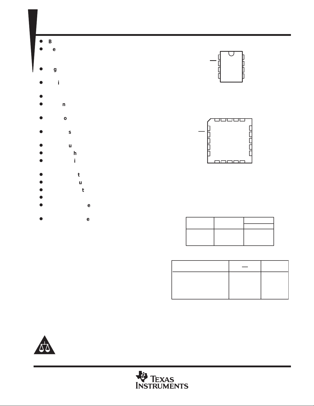
D, JG, OR P PACKAGE
(TOP VIEW)
R
1
RE
2
DE
3
4
D
FK PACKAGE
(TOP VIEW)
NCRNC
3212019
4
5
6
7
8
910111213
NCDNC
8
7
6
5
CC
V
GND
V
B
A
GND
NC
18
17
16
15
14
NC
CC
Function Tables
DRIVER
ENABLE
DE
H
H
L
RECEIVER
low level,
high impedance (off)
? =
OUTPUTS
ENABLE
RE
L
L
L
H
L
indeterminate,
NC
B
NC
A
NC
A B
H L
L H
Z Z
OUTPUT
R
H
?
L
Z
H
Please be aware that an important notice concerning availability, standard warranty, and use in critical applications of
Texas Instruments semiconductor products and disclaimers thereto appears at the end of this data sheet.
LinBiCMOS and LinASIC are trademarks of Texas Instruments Incorporated.
PRODUCTION DATA information is current as of publication date.
Products conform to specifications per the terms of Texas Instruments
standard warranty. Production processing does not necessarily include
testing of all parameters.
POST OFFICE BOX 655303 • DALLAS, TEXAS 75265
Copyright 2000, Texas Instruments Incorporated
On products compliant to MIL-PRF-38535, all parameters are tested
unless otherwise noted. On all other products, production
processing does not necessarily include testing of all parameters.
1
SN55LBC176, SN65LBC176, SN65LBC176Q, SN75LBC176
DIFFERENTIAL BUS TRANSCEIVERS
SLLS067F – AUGUST 1990 – REVISED JANUARY 2000
description (continued)
The SN55LBC176, SN65LBC176, SN65LBC176Q, and SN75LBC176 combine a 3-state, differential line driver
and a differential input line receiver, both of which operate from a single 5-V power supply. The driver and
receiver have active-high and active-low enables, respectively, which can externally connect together to
function as a direction control. The driver differential outputs and the receiver differential inputs connect
internally to form a differential input/output (I/O) bus port that is designed to offer minimum loading to the bus
whenever the driver is disabled or V
ranges, making the device suitable for party-line applications. Very low device supply current can be achieved
by disabling the driver and the receiver. Both the driver and receiver are available as cells in the Texas
Instruments LinASIC Library.
These transceivers are suitable for ANSI Standard RS-485 and ISO 8482:1987 (E) applications to the extent
that they are specified in the operating conditions and characteristics section of this data sheet. Certain limits
contained in the ANSI Standard RS-485 and ISO 8482:1987 (E) are not met or cannot be tested over the entire
military temperature range.
The SN55LBC176 is characterized for operation from –55°C to 125°C. The SN65LBC176 is characterized for
operation from –40°C to 85°C, and the SN65LBC176Q is characterized for operation from –40°C to 125°C.
The SN75LBC176 is characterized for operation from 0°C to 70°C.
= 0. This port features wide positive and negative common-mode voltage
CC
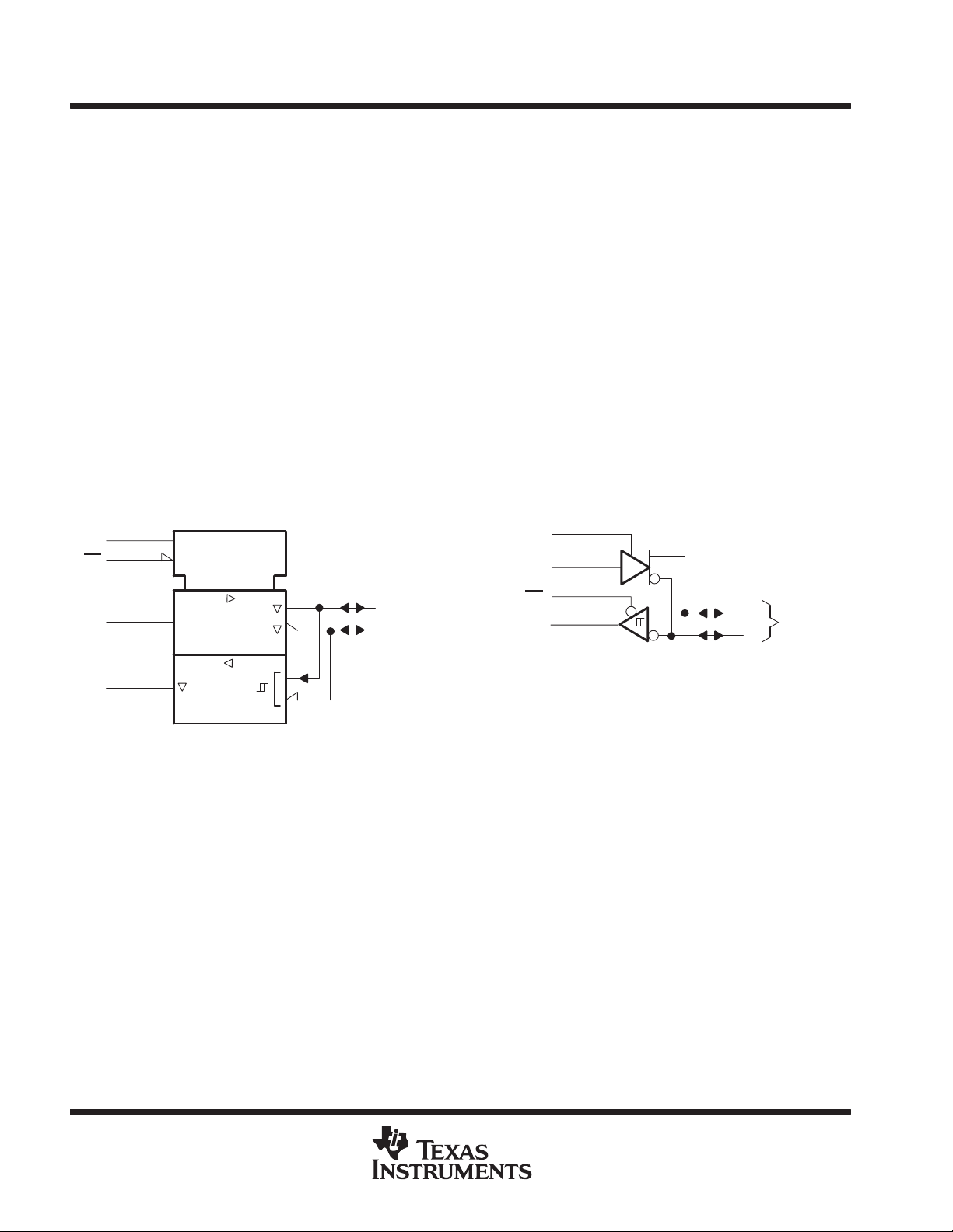
logic symbol
3
DE
2
RE
4
D
1
R
†
This symbol is in accordance with ANSI/IEEE Std 91-1984 and
IEC Publication 617-12.
†
EN1
EN2
6
1
1
2
A
7
B
logic diagram (positive logic)
3
DE
4
D
2
RE
1
R
6
A
7
Bus
B
2
POST OFFICE BOX 655303 • DALLAS, TEXAS 75265
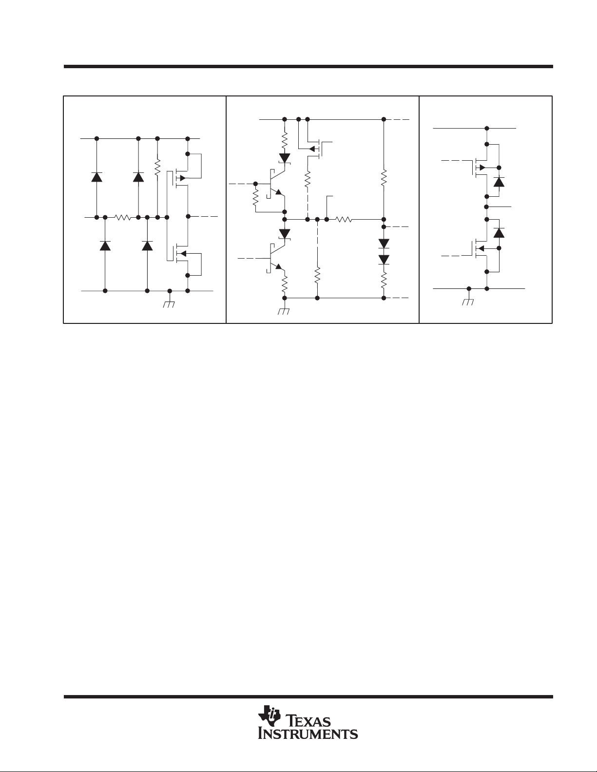
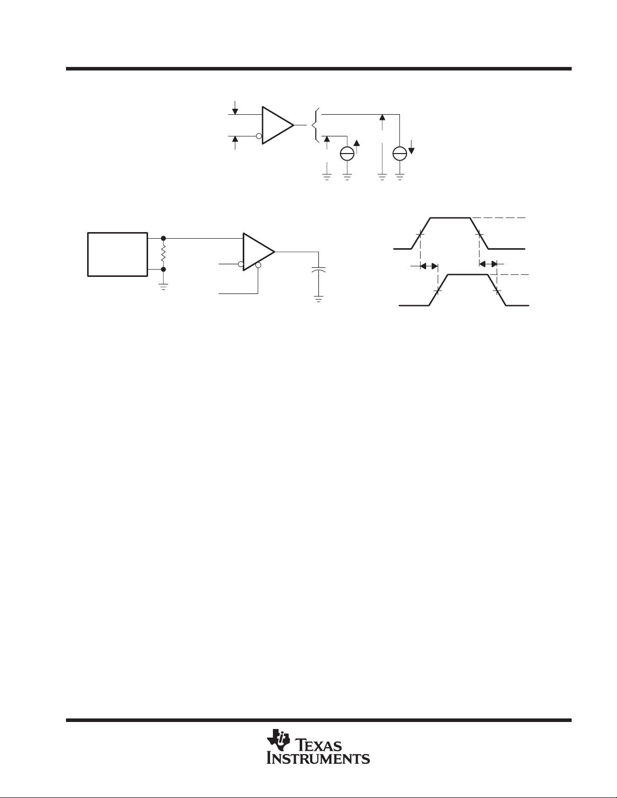
schematics of inputs and outputs
SN55LBC176, SN65LBC176, SN65LBC176Q, SN75LBC176
DIFFERENTIAL BUS TRANSCEIVERS
SLLS067F – AUGUST 1990 – REVISED JANUARY 2000
EQUIVALENT OF EACH INPUT TYPICAL OF RECEIVER OUTPUT
V
V
CC
Input
TYPICAL OF A AND B I/O PORTS
CC
100 kΩ NOM
A Port Only
100 kΩ NOM
B Port Only
3 kΩ
NOM
A or B
18 kΩ
NOM
1.1 kΩ
NOM
V
CC
Output
POST OFFICE BOX 655303 • DALLAS, TEXAS 75265
3
SN55LBC176, SN65LBC176, SN65LBC176Q, SN75LBC176
Voltage at any bus terminal (separately or common mode), V
V
V
High-level output current, I
Low-level output current, I
mA
Operating free-air temperature, T
°C
DIFFERENTIAL BUS TRANSCEIVERS
SLLS067F – AUGUST 1990 – REVISED JANUARY 2000
absolute maximum ratings over operating free-air temperature range (unless otherwise noted)
Supply voltage, VCC (see Note 1) 7 V. . . . . . . . . . . . . . . . . . . . . . . . . . . . . . . . . . . . . . . . . . . . . . . . . . . . . . . . . . . . .
Voltage range at any bus terminal –10 V to 15 V. . . . . . . . . . . . . . . . . . . . . . . . . . . . . . . . . . . . . . . . . . . . . . . . . . . .
Input voltage, VI (D, DE, R, or RE) –0.3 V to VCC + 0.5 V. . . . . . . . . . . . . . . . . . . . . . . . . . . . . . . . . . . . . . . . . . . .
Continuous total power dissipation See Dissipation Rating Table. . . . . . . . . . . . . . . . . . . . . . . . . . . . . . . . . . . . .
Operating free-air temperature range, T
Storage temperature range, T
–65°C to 150°C. . . . . . . . . . . . . . . . . . . . . . . . . . . . . . . . . . . . . . . . . . . . . . . . . . .
stg
Lead temperature 1,6 mm (1/16 inch) from case for 10 seconds 260°C. . . . . . . . . . . . . . . . . . . . . . . . . . . . . . .
†
Stresses beyond those listed under “absolute maximum ratings” may cause permanent damage to the device. These are stress ratings only, and
functional operation of the device at these or any other conditions beyond those indicated under “recommended operating conditions” is not
implied. Exposure to absolute-maximum-rated conditions for extended periods may affect device reliability.
NOTE 1: All voltage values, except differential I/O bus voltage, are with respect to network ground terminal.
PACKAGE
D 725 mW 5.8 mW/°C 464 mW 377 mW —
FK 1375 mW 11.0 mW/°C 880 mW 715 mW 440 mW
JG 1050 mW 8.4 mW/°C 672 mW 546 mW 210 mW
P 1000 mW 8.0 mW/°C 640 mW 520 mW —
TA ≤ 25°C
POWER RATING
DERATING FACTOR
: SN55LBC176 –55°C to 125°C. . . . . . . . . . . . . . . . . . . . . . . . . . . . . .
A
SN65LBC176 –40°C to 85°C. . . . . . . . . . . . . . . . . . . . . . . . . . . . . . .
SN65LBC176Q –40°C to 125°C. . . . . . . . . . . . . . . . . . . . . . . . . . . . .
SN75LBC176 0°C to 70°C. . . . . . . . . . . . . . . . . . . . . . . . . . . . . . . . .
DISSIPATION RATING TABLE
ABOVE TA = 25°C
TA = 70°C
POWER RATING
TA = 85°C
POWER RATING
TA = 110°C
POWER RATING
†
recommended operating conditions
MIN NOM MAX UNIT
Supply voltage, V
High-level input voltage, V
Low-level input voltage, V
Differential input voltage, VID (see Note 2) ±12 V
p
NOTE 2: Differential input/output bus voltage is measured at the noninverting terminal A with respect to the inverting terminal B.
CC
p
IH
IL
p
p
OH
OL
p
A
or
I
IC
D, DE, and RE 2 V
D, DE, and RE 0.8 V
Driver –60 mA
Receiver –400 µA
Driver 60
Receiver 8
SN55LBC176 –55 125
SN65LBC176 –40 85
SN65LBC176Q –40 125
SN75LBC176 0 70
4.75 5 5.25 V
12
–7
°
4
POST OFFICE BOX 655303 • DALLAS, TEXAS 75265
SN55LBC176, SN65LBC176, SN65LBC176Q, SN75LBC176
,
,
,
55LBC176,
| V
|
Diff
R
L
Ω,
See Figure 1,
V
65LCB176
1.1
VOCCommon-mode output voltage
R
100 Ω
See Figure 1
V
IOOutput current
,
mA
IOSShort-circuit output current
mA
250
ICCSupply current
ICC
mA
DIFFERENTIAL BUS TRANSCEIVERS
SLLS067F – AUGUST 1990 – REVISED JANUARY 2000
DRIVER SECTION
electrical characteristics over recommended ranges of supply voltage and operating free-air
temperature (unless otherwise noted)
PARAMETER TEST CONDITIONS MIN MAX UNIT
V
IK
V
O
| V
OD1
OD2
V
OD3
∆| VOD |
∆| VOC |
I
IH
I
IL
†
∆ | VOD | and ∆ | VOC | are the changes in magnitude of VOD and VOC, respectively, that occur when the input changes from a high level to a
low level.
NOTES: 3. This device meets the ANSI Standard RS-485 VOD requirements above 0°C only.
Input clamp voltage II = –18 mA –1.5 V
Output voltage IO = 0 0 6 V
| Differential output voltage IO = 0 1.5 6 V
55LBC176
R
= 54 Ω
erential output voltage
Differential output voltage
Change in magnitude of differential
output voltage
Change in magnitude of
common-mode output voltage
p
High-level input current VI = 2.4 V –100 µA
Low-level input current VI = 0.4 V –100 µA
pp
4. This applies for both power on and off; refer to ANSI Standard RS-485 for exact conditions.
†
p
†
p
54
See Note 3
V
= –7 V to 12 V,
test
See Note 3
= 54 Ω or
L
Output disabled,
See Note 4
VO = –7 V –250
VO = 0 –150
VO = V
CC
VO = 12 V
VI = 0 or VCC,
No load
See Figure 1
See Figure 2,
,
VO = 12 V 1
VO = –7 V –0.8
Receiver disabled
and driver enabled
Receiver and driver
disabled
65LBC176,
65LBC176Q
75LBC176 1.5 5
55LCB176,
65LBC176Q
75LBC176 1.5 5
55LBC176,
65LBC176Q
65LBC176,
75LBC176
55LBC176,
65LBC176Q
65LBC176,
75LBC176
1.1
,
±0.2 V
3
–1
±0.2 V
1.75
1.5
0.25
0.2
V
POST OFFICE BOX 655303 • DALLAS, TEXAS 75265
5

SN55LBC176, SN65LBC176, SN65LBC176Q, SN75LBC176
See Figure 3
DIFFERENTIAL BUS TRANSCEIVERS
SLLS067F – AUGUST 1990 – REVISED JANUARY 2000
switching characteristics over recommended ranges of supply voltage and operating free-air
temperature
PARAMETER TEST CONDITIONS
t
d(OD)
t
t(OD)
t
sk(p)
t
PZH
t
PZL
t
PHZ
t
PLZ
†
All typical values are at VCC = 5 V, TA = 25°C.
Differential output delay time
Differential output transition time
Pulse skew (| t
Output enable time to high level RL = 110 Ω, See Figure 4 65 35 ns
Output enable time to low level RL = 110 Ω, See Figure 5 65 35 ns
Output disable time from high level RL = 110 Ω, See Figure 4 105 60 ns
Output disable time from low level RL = 110 Ω, See Figure 5 105 35 ns
d(ODH)
– t
d(ODL)
DATA SHEET PARAMETER RS-485
RL = 54 Ω,
|)
V
O
| V
OD1
| V
OD2
| V
OD3
∆ | VOD | || Vt | – | Vt ||
V
OC
∆ | VOC | | Vos – Vos |
I
OS
I
O
CL = 50 pF,
SYMBOL EQUIVALENTS
Voa, V
| V
| Vt (RL = 54 Ω)
|
Vt (test termination
measurement 2)
SN55LBC176
SN65LBC176Q
MIN TYP MAX MIN TYP†MAX
8 31 8 25 ns
12 12 ns
ob
o
| Vos |
None
Iia, I
ib
SN65LBC176
SN75LBC176
6 0 6 ns
UNIT
6
POST OFFICE BOX 655303 • DALLAS, TEXAS 75265

SN55LBC176, SN65LBC176, SN65LBC176Q, SN75LBC176
VOHHigh-level output voltage
ID
,
OH
µ ,
2.7
V
VOLLow-level output voltage
ID
,
OL
,
0.45
V
IILine input current
,
mA
CC
y
No load
R
SN65LBC176
0.25
See Figure 8
See Figure 8
DIFFERENTIAL BUS TRANSCEIVERS
SLLS067F – AUGUST 1990 – REVISED JANUARY 2000
RECEIVER SECTION
electrical characteristics over recommended ranges of common-mode input voltage, supply
voltage, and operating free-air temperature (unless otherwise noted)
PARAMETER TEST CONDITIONS MIN
Positive-going input threshold
V
IT+
voltage
Negative-going input threshold
V
IT–
voltage
Hysteresis voltage (V
V
hys
(see Figure 4)
V
Enable-input clamp voltage II = –18 mA –1.5 V
IK
p
p
High-impedance-state output
I
OZ
current
p
I
High-level enable-input current VIH = 2.7 V –100 µA
IH
I
Low-level enable-input current VIL = 0.4 V –100 µA
IL
r
Input resistance 12 kΩ
I
I
Supply current
CC
†
All typical values are at VCC = 5 V, TA = 25°C.
‡
The algebraic convention, in which the less-positive (more-negative) limit is designated minimum, is used in this data sheet for common-mode
input voltage and threshold voltage levels only .
NOTE 5: This applies for both power on and power off. Refer to ANSI Standard RS-485 for exact conditions.
IT+
– V
IT–
VO = 2.7 V, IO = –0.4 mA 0.2 V
VO = 0.5 V, IO = 8 mA –0.2
)
V
= 200 mV, I
See Figure 6
V
= 200 mV, I
See Figure 6
VO = 0.4 V to 2.4 V ±20 µA
Other input = 0 V,
See Note 5
VI = 0 or VCC,
= –400 µA,
= 8 mA,
VI = 12 V 1
VI = –7 V –0.8
Receiver enabled
and driver disabled
eceiver and
driver disabled
SN55LBC176,
SN65LBC176Q
SN75LBC176 0.2
,
‡
†
TYP
MAX UNIT
50 mV
3.9 mA
V
mA
switching characteristics over recommended ranges of supply voltage and operating free-air
temperature, C
t
PLH
t
PHL
t
sk(p)
t
PZH
t
PZL
t
PHZ
t
PLZ
†
All typical values are at VCC = 5 V, TA = 25°C.
= 15 pF
L
PARAMETER TEST CONDITIONS
Propagation delay time, low- to high-level
single-ended output
Propagation delay time, high- to low-level
single-ended output
Pulse skew (| t
Output enable time to high level
Output enable time to low level
Output disable time from high level
Output disable time from low level
d(ODH)
– t
|) 10 3 6 ns
d(ODL)
SN65LBC176Q
VID = –1.5 V to 1.5 V,
See Figure 7
POST OFFICE BOX 655303 • DALLAS, TEXAS 75265
SN55LBC176
MIN MAX MIN TYP†MAX
11 37 11 33 ns
11 37 11 33 ns
35 35 ns
35 30 ns
35 35 ns
35 30 ns
SN65LBC176
SN75LBC176
UNIT
7

SN55LBC176, SN65LBC176, SN65LBC176Q, SN75LBC176
DIFFERENTIAL BUS TRANSCEIVERS
SLLS067F – AUGUST 1990 – REVISED JANUARY 2000
PARAMETER MEASUREMENT INFORMATION
R
L
V
OD2
2
R
L
V
OC
2
V
OD3
375 Ω
60 Ω
375 Ω
V
test
Figure 1. Driver VOD and V
Generator
(see Note A)
0 V or 3 V
Generator
(see Note A)
50 Ω
50 Ω
Figure 2. Driver V
Input
t
d(ODH)
Output
t
t(OD)
3 V
TEST CIRCUIT
OC
RL = 54 Ω
CL = 50 pF
(see Note B)
Output
Figure 3. Driver Test Circuit and Voltage Waveforms
Output
Input
Output
CL = 50 pF
(see Note B)
TEST CIRCUIT
S1
RL = 110 Ω
OD3
1.5 V
50%
VOLTAGE WA VEFORMS
1.5 V
1.5 V
t
PZH
2.3 V
t
PHZ
VOLTAGE WA VEFORMS
90%
10%
1.5 V
50%
0.5 V
3 V
0 V
t
d(ODL)
≈ 2.5 V
≈ – 2.5 V
t
t(OD)
3 V
0 V
V
OH
V
off
≈ 0 V
Figure 4. Driver Test Circuit and Voltage Waveforms
3 V or 0 V
Generator
(see Note A)
50 Ω
CL = 50 pF
(see Note B)
TEST CIRCUIT
S1
5 V
RL = 110 Ω
Output
Input
t
PZL
Output
1.5 V
VOLTAGE WAVEFORMS
1.5 V
2.3 V
t
PLZ
3 V
0 V
5 V
0.5 V
V
OL
Figure 5. Driver Test Circuit and Voltage Waveforms
NOTES: A. The input pulse is supplied by a generator having the following characteristics: PRR ≤ 1 MHz, 50% duty cycle, tr ≤ 6 ns, tf ≤ 6 ns,
8
ZO=50Ω.
B. CL includes probe and jig capacitance.
POST OFFICE BOX 655303 • DALLAS, TEXAS 75265
SN55LBC176, SN65LBC176, SN65LBC176Q, SN75LBC176
DIFFERENTIAL BUS TRANSCEIVERS
SLLS067F – AUGUST 1990 – REVISED JANUARY 2000
PARAMETER MEASUREMENT INFORMATION
V
ID
V
OL
+I
OL
V
OH
–I
OH
Figure 6. Receiver VOH and V
Generator
(see Note A)
NOTES: A. The input pulse is supplied by a generator having the following characteristics: PRR ≤ 1 MHz, 50% duty cycle, tr ≤ 6 ns, tf ≤ 6 ns,
ZO=50Ω.
B. CL includes probe and jig capacitance.
51 Ω
1.5 V
0 V
TEST CIRCUIT
Output
CL = 15 pF
(see Note B)
OL
Input
t
Output
1.5 V
PLH
1.3 V
VOLTAGE WAVEFORMS
1.5 V
t
PHL
1.3 V
3 V
0 V
V
V
OH
OL
Figure 7. Receiver Test Circuit and Voltage Waveforms
POST OFFICE BOX 655303 • DALLAS, TEXAS 75265
9
SN55LBC176, SN65LBC176, SN65LBC176Q, SN75LBC176
DIFFERENTIAL BUS TRANSCEIVERS
SLLS067F – AUGUST 1990 – REVISED JANUARY 2000
PARAMETER MEASUREMENT INFORMATION
Input
Output
1.5 V
–1.5 V
Generator
(see Note A)
t
PZH
S1
50 Ω
1.5 V
1.5 V
3 V
S1 to 1.5 V
S2 Open
S3 Closed
0 V
V
OH
0 V
CL = 15 pF
(see Note B)
TEST CIRCUIT
Input
Output
5 kΩ
2 kΩ
1N916 or Equivalent
S3
t
PZL
S2
1.5 V
1.5 V
5 V
3 V
S1 to –1.5 V
S2 Closed
S3 Opened
0 V
≈ 4.5 V
V
OL
3 V
S1 to –1.5 V
S2 Closed
0 V
≈ 1.3 V
V
OL
Input
Output
t
PHZ
0.5 V
1.5 V
3 V
S1 to 1.5 V
S2 Closed
S3 Closed S3 Closed
0 V
V
OH
≈ 1.3 V
VOLTAGE WAVEFORMS
Input
Output
t
PLZ
1.5 V
0.5 V
Figure 8. Receiver Test Circuit and Voltage Waveforms
NOTES: A. The input pulse is supplied by a generator having the following characteristics: PRR ≤ 1 MHz, 50% duty cycle, tr ≤ 6 ns, tf ≤ 6 ns,
ZO=50Ω.
B. CL includes probe and jig capacitance.
10
POST OFFICE BOX 655303 • DALLAS, TEXAS 75265

SN55LBC176, SN65LBC176, SN65LBC176Q, SN75LBC176
DIFFERENTIAL BUS TRANSCEIVERS
SLLS067F – AUGUST 1990 – REVISED JANUARY 2000
MECHANICAL INFORMATION
D (R-PDSO-G**) PLASTIC SMALL-OUTLINE PACKAGE
14 PINS SHOWN
0.050 (1,27)
14
1
0.069 (1,75) MAX
A
0.020 (0,51)
0.014 (0,35)
0.010 (0,25)
0.004 (0,10)
DIM
8
7
PINS **
0.010 (0,25)
0.157 (4,00)
0.150 (3,81)
M
0.244 (6,20)
0.228 (5,80)
Seating Plane
0.004 (0,10)
8
14
0.008 (0,20) NOM
0°–8°
16
Gage Plane
0.010 (0,25)
0.044 (1,12)
0.016 (0,40)
A MAX
A MIN
NOTES: A. All linear dimensions are in inches (millimeters).
B. This drawing is subject to change without notice.
C. Body dimensions do not include mold flash or protrusion, not to exceed 0.006 (0,15).
D. Falls within JEDEC MS-012
POST OFFICE BOX 655303 • DALLAS, TEXAS 75265
0.197
(5,00)
0.189
(4,80)
0.344
(8,75)
0.337
(8,55)
0.394
(10,00)
0.386
(9,80)
4040047/D 10/96
11
SN55LBC176, SN65LBC176, SN65LBC176Q, SN75LBC176
DIFFERENTIAL BUS TRANSCEIVERS
SLLS067F – AUGUST 1990 – REVISED JANUARY 2000
MECHANICAL INFORMATION
FK (S-CQCC-N**) LEADLESS CERAMIC CHIP CARRIER
28 TERMINALS SHOWN
A SQ
B SQ
20
22
23
24
25
19
21
12826 27
12
1314151618 17
0.020 (0,51)
0.010 (0,25)
MIN
0.342
(8,69)
0.442
0.640
0.740
0.938
1.141
A
0.358
(9,09)
0.458
(11,63)
0.660
(16,76)
0.761
(19,32)(18,78)
0.962
(24,43)
1.165
(29,59)
NO. OF
TERMINALS
**
11
10
9
8
7
6
5
432
20
28
44
52
68
84
0.020 (0,51)
0.010 (0,25)
(11,23)
(16,26)
(23,83)
(28,99)
MINMAX
0.307
(7,80)
0.406
(10,31)
0.495
(12,58)
0.495
(12,58)
0.850
(21,6)
1.047
(26,6)
0.080 (2,03)
0.064 (1,63)
B
MAX
0.358
(9,09)
0.458
(11,63)
0.560
(14,22)
0.560
(14,22)
0.858
(21,8)
1.063
(27,0)
0.055 (1,40)
0.045 (1,14)
0.028 (0,71)
0.022 (0,54)
0.050 (1,27)
NOTES: A. All linear dimensions are in inches (millimeters).
12
B. This drawing is subject to change without notice.
C. This package can be hermetically sealed with a metal lid.
D. The terminals are gold-plated.
E. Falls within JEDEC MS-004
POST OFFICE BOX 655303 • DALLAS, TEXAS 75265
0.045 (1,14)
0.035 (0,89)
0.045 (1,14)
0.035 (0,89)
4040140/C 11/95
SN55LBC176, SN65LBC176, SN65LBC176Q, SN75LBC176
DIFFERENTIAL BUS TRANSCEIVERS
SLLS067F – AUGUST 1990 – REVISED JANUARY 2000
MECHANICAL INFORMATION
JG (R-GDIP-T8) CERAMIC DUAL-IN-LINE PACKAGE
0.400 (10,20)
0.355 (9,00)
0.063 (1,60)
0.015 (0,38)
0.100 (2,54)
8
1
5
4
0.065 (1,65)
0.045 (1,14)
0.020 (0,51) MIN
0.280 (7,11)
0.245 (6,22)
0.200 (5,08) MAX
0.130 (3,30) MIN
0.023 (0,58)
0.015 (0,38)
0.310 (7,87)
0.290 (7,37)
Seating Plane
0°–15°
0.014 (0,36)
0.008 (0,20)
NOTES: A. All linear dimensions are in inches (millimeters).
B. This drawing is subject to change without notice.
C. This package can be hermetically sealed with a ceramic lid using glass frit.
D. Index point is provided on cap for terminal identification only on press ceramic glass frit seal only.
E. Falls within MIL-STD-1835 GDIP1-T8
POST OFFICE BOX 655303 • DALLAS, TEXAS 75265
4040107/C 08/96
13

MECHANICAL DATA
MPDI001A – JANUARY 1995 – REVISED JUNE 1999
MECHANICAL INFORMATION
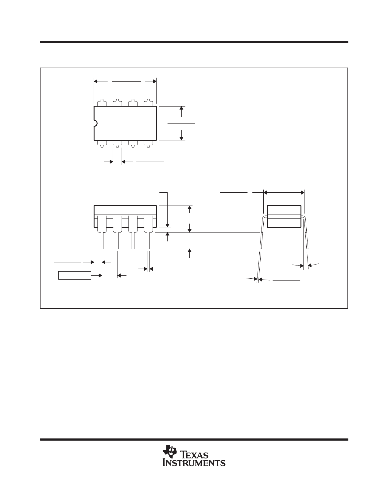
P (R-PDIP-T8) PLASTIC DUAL-IN-LINE
0.400 (10,60)
0.355 (9,02)
8
5
0.260 (6,60)
0.240 (6,10)
1
0.021 (0,53)
0.015 (0,38)
NOTES: A. All linear dimensions are in inches (millimeters).
B. This drawing is subject to change without notice.
C. Falls within JEDEC MS-001
4
0.070 (1,78) MAX
0.020 (0,51) MIN
0.200 (5,08) MAX
0.125 (3,18) MIN
0.100 (2,54)
0.010 (0,25)
Seating Plane
M
0.325 (8,26)
0.300 (7,62)
0.015 (0,38)
Gage Plane
0.010 (0,25) NOM
0.430 (10,92)
MAX
4040082/D 05/98
For the latest package information, go to http://www.ti.com/sc/docs/package/pkg_info.htm
14
POST OFFICE BOX 655303 • DALLAS, TEXAS 75265

IMPORTANT NOTICE
T exas Instruments and its subsidiaries (TI) reserve the right to make changes to their products or to discontinue
any product or service without notice, and advise customers to obtain the latest version of relevant information
to verify, before placing orders, that information being relied on is current and complete. All products are sold
subject to the terms and conditions of sale supplied at the time of order acknowledgement, including those
pertaining to warranty, patent infringement, and limitation of liability.
TI warrants performance of its semiconductor products to the specifications applicable at the time of sale in
accordance with TI’s standard warranty. Testing and other quality control techniques are utilized to the extent
TI deems necessary to support this warranty . Specific testing of all parameters of each device is not necessarily
performed, except those mandated by government requirements.
CERTAIN APPLICATIONS USING SEMICONDUCTOR PRODUCTS MAY INVOLVE POTENTIAL RISKS OF
DEATH, PERSONAL INJURY, OR SEVERE PROPERTY OR ENVIRONMENTAL DAMAGE (“CRITICAL
APPLICATIONS”). TI SEMICONDUCTOR PRODUCTS ARE NOT DESIGNED, AUTHORIZED, OR
WARRANTED TO BE SUITABLE FOR USE IN LIFE-SUPPORT DEVICES OR SYSTEMS OR OTHER
CRITICAL APPLICA TIONS. INCLUSION OF TI PRODUCTS IN SUCH APPLICATIONS IS UNDERST OOD TO
BE FULLY AT THE CUSTOMER’S RISK.
In order to minimize risks associated with the customer’s applications, adequate design and operating
safeguards must be provided by the customer to minimize inherent or procedural hazards.
TI assumes no liability for applications assistance or customer product design. TI does not warrant or represent
that any license, either express or implied, is granted under any patent right, copyright, mask work right, or other
intellectual property right of TI covering or relating to any combination, machine, or process in which such
semiconductor products or services might be or are used. TI’s publication of information regarding any third
party’s products or services does not constitute TI’s approval, warranty or endorsement thereof.
Copyright 2000, Texas Instruments Incorporated
 Loading...