

www.ti.com
SN65HVD54
SN65HVD52
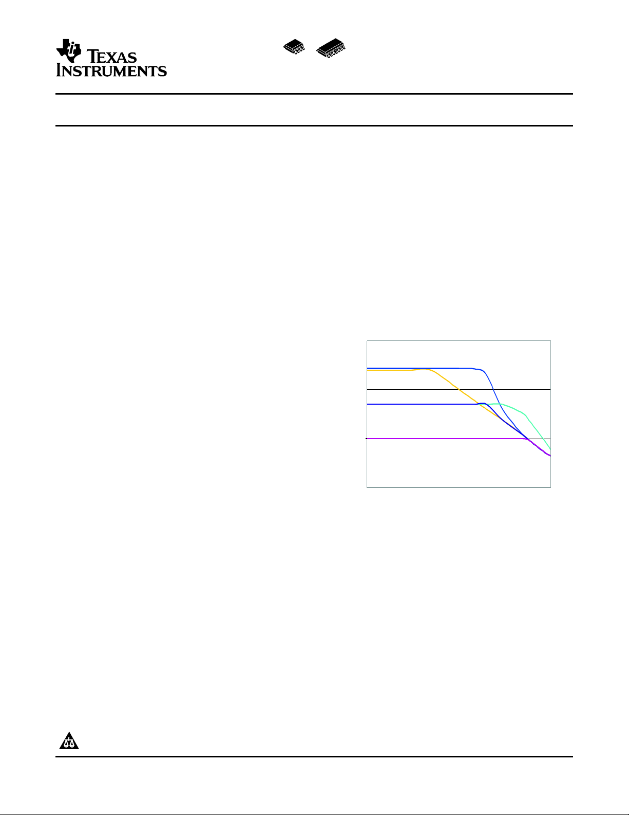
0.1
1
10
100
10 100 1000
Cable Length (meters)
Signalling Rate (Mbps)
SN65HVD56
SN65HVD58
SN65HVD50
SN65HVD53
SN65HVD51
SN65HVD55
SN65HVD57
SN65HVD59
HIGH OUTPUT FULL-DUPLEX RS-485 DRIVERS AND RECEIVERS
SN65HVD50-SN65HVD55
SN65HVD56-SN65HVD59
SLLS666 – SEPTEMBER 2005
FEATURES
• 1/8 Unit-Load Option Available (Up to 256
Nodes on the Bus)
• Bus-Pin ESD Protection Exceeds 15 kV HBM
• Optional Driver Output Transition Times for
Signaling Rates
(1)
of 1 Mbps, 5 Mbps and 25
Mbps
• Low-Current Standby Mode < 1 µ A
• Glitch-Free Power-Up and Power-Down Bus
I/Os
• Bus Idle, Open, and Short Circuit Failsafe
• Meets or exceeds the requirements of ANSI
TIA/EIA-485-A and RS-422 Compatible
• 3.3-V Devices available, SN65HVD30-39
APPLICATIONS
• Utility Meters
• Chassis-to-Chassis Interconnects
• DTE/DCE Interfaces
• Industrial, Process, and Building Automation
• Point-of-Sale (POS) Terminals and Networks
The SN65HVD50, SN65HVD51, SN65HVD52,
SN65HVD56 and SN65HVD57 are fully enabled with
no external enabling pins. The SN65HVD56 and
SN65HVD57 implement receiver equalization
technology for improved performance in long distance
applications.
The SN65HVD53, SN65HVD54, SN65HVD55,
SN65HVD58, and SN65HVD59 have active-high
driver enables and active-low receiver enables. A
very low, less than 1 uA, standby current can be
achieved by disabling both the driver and receiver.
The SN65HVD58 and SN65HVD59 implement
receiver equalization technology for improved
performance in long distance applications.
All devices are characterized for operation from -40°
C to +85°.
DESCRIPTION
The SN65HVD5X devices are 3-state differential line
drivers and differential-input line receivers that
operate with a 5-V power supply. Each driver and
receiver has separate input and output pins for
full-duplex bus communication designs. They are
designed for balanced transmission lines and
interoperation with ANSI TIA/EIA-485A,
TIA/EIA-422-B, ITU-T v.11 and ISO 8482:1993
standard-compliant devices.
(1) The signaling rate of a line is the number of voltage
transitions that are made per second expressed in the units
bps (bits per second). to 1000 meters.
Please be aware that an important notice concerning availability, standard warranty, and use in critical applications of Texas
Instruments semiconductor products and disclaimers thereto appears at the end of this data sheet.
UNLESS OTHERWISE NOTED this document contains
PRODUCTION DATA information current as of publication date.
Products conform to specifications per the terms of Texas
Instruments standard warranty. Production processing does not
necessarily include testing of all parameters.
The SN65HVD56 and SN65HVD58 implement
receiver equalization technology for improved jitter
performance on differential bus applications with data
rates up to 20 Mbps at cable lengths up to 160
meters.
The SN65HVD57 and SN65HVD59 implement
receiver equalization technology for improved jitter
performance on differential bus applications with data
rates in the range of 1 to 5 Mbps at cable lengths up
Copyright © 2005, Texas Instruments Incorporated
www.ti.com
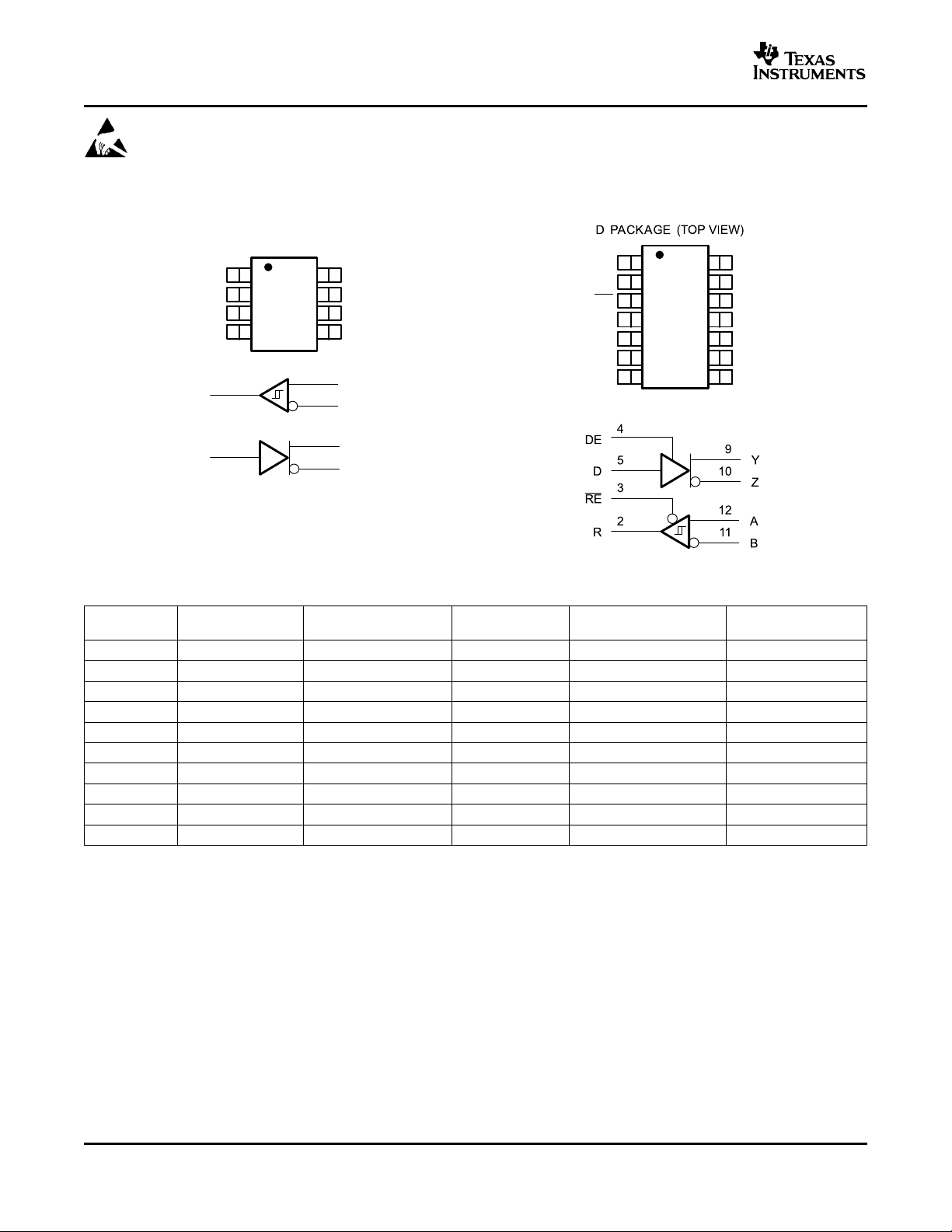
R
D
B
A
Z
Y
7
8
6
5
2
3
D P (TOP VIEW)ACKAGE
1
2
3
4
8
7
6
5
R
D
V
CC
B
A
Z
Y
GND
1
2
3
4
5
6
7
14
13
12
11
10
9
8
NC
R
RE
DE
D
GND
GND
V
CC
V
CC
A
B
Z
Y
NC
NC - No internal connection
SN65HVD50-SN65HVD55
SN65HVD56-SN65HVD59
SLLS666 – SEPTEMBER 2005
These devices have limited built-in ESD protection. The leads should be shorted together or the device
placed in conductive foam during storage or handling to prevent electrostatic damage to the MOS gates.
SN65HVD50, SN65HVD51, SN65HVD52, SN65HVD56, SN65HVD53, SN65HVD54, SN65HVD55, SN65HVD58,
SN65HVD57 SN65HVD59
AVAILABLE OPTIONS
SIGNALING RECEIVER BASE
RATE EQUALIZATION PART NUMBER
25 Mbps 1/2 No No SN65HVD50 PREVIEW
5 Mbps 1/8 No No SN65HVD51 PREVIEW
1 Mbps 1/8 No No SN65HVD52 PREVIEW
25 Mbps 1/2 No Yes SN65HVD53 65HVD53
5 Mbps 1/8 No Yes SN65HVD54 65HVD54
1 Mbps 1/8 No Yes SN65HVD55 65HVD55
25 Mbps 1/2 Yes No SN65HVD56 PREVIEW
5 Mbps 1/8 Yes No SN65HVD57 PREVIEW
25 Mbps 1/2 Yes Yes SN65HVD58 PREVIEW
5 Mbps 1/8 Yes Yes SN65HVD59 PREVIEW
UNIT LOADS ENABLES SOIC MARKING
2
www.ti.com
SN65HVD50-SN65HVD55
SN65HVD56-SN65HVD59
SLLS666 – SEPTEMBER 2005
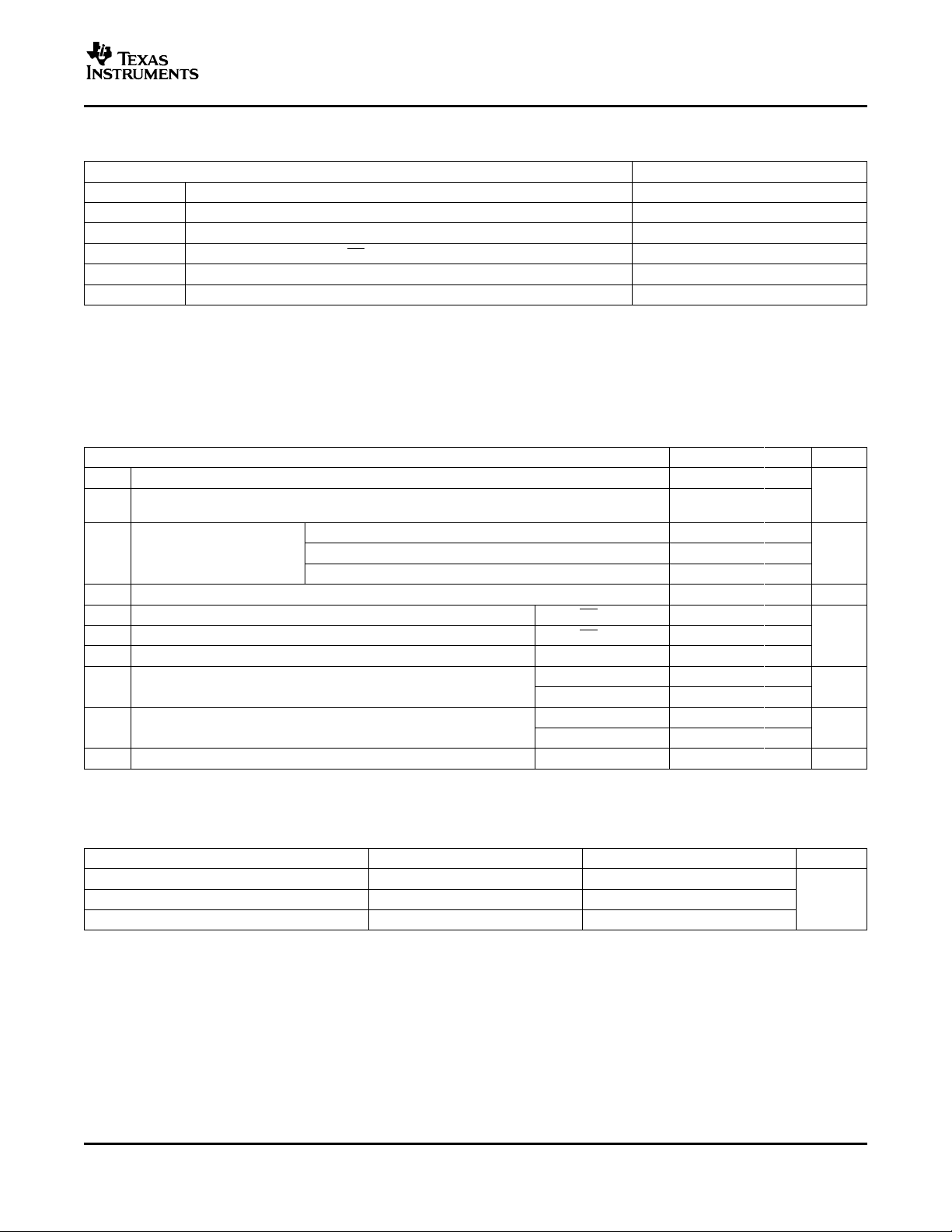
ABSOLUTE MAXIMUM RATINGS
over operating free-air temperature range (unless otherwise noted)
V
CC
V
I
I
O
(1) Stresses beyond those listed under absolute maximum ratings may cause permanent damage to the device. These are stress ratings
only, and functional operation of the device at these or any other conditions beyond those indicated under recommended operating
conditions is not implied. Exposure to absolute-maximum-rated conditions for extended periods may affect device reliability.
(2) All voltage values, except differential I/O bus voltages, are with respect to network ground terminal.
(3) This tests survivability only and the output state of the receiver is not specified.
Supply voltage range –0.3 V to 6 V
Voltage range at any bus terminal (A, B, Y, Z) –9 V to 14 V
Voltage input, transient pulse through 100 Ω . See Figure 12 (A, B, Y, Z)
Voltage input range (D, DE, RE) -0.5 V to 7 V
Continuous total power dissipation Internally limited
Output current (receiver output only, R) 11 mA
RECOMMENDED OPERATING CONDITIONS
over operating free-air temperature range (unless otherwise noted)
PARAMETER MIN NOM MAX UNIT
V
VIor Voltage at any bus terminal (separately or common mode) –7
V
1/t
R
V
V
V
I
I
T
(1) The algebraic convention, in which the least positive (most negative) limit is designated as minimum is used in this data sheet.
(2) See thermal characteristics table for information regarding this specification.
Supply voltage 4.5 5.5
CC
IC
UI
SN65HVD50, SN65HVD53, SN65HVD56, SN65HVD58 25
Signaling rate SN65HVD51, SN65HVD54, SN65HVD57, SN65HVD59 5 Mbps
SN65HVD52, SN65HVD55 1
Differential load resistance 54 60 Ω
L
High-level input voltage D, DE, RE 2 V
IH
Low-level input voltage D, DE, RE 0 0.8 V
IL
Differential input voltage -12 12
ID
High-level output current mA
OH
Low-level output current mA
OL
(2)
Junction temperature –40 150 ° C
J
(1) (2)
(3)
(1)
Driver -60
Receiver –8
Driver 60
Receiver 8
UNIT
–50 to 50 V
V
12
CC
ELECTROSTATIC DISCHARGE PROTECTION
PARAMETER TEST CONDITIONS MIN TYP
Human body model Bus terminals and GND ± 16
Human body model
Charged-device-model
(1) All typical values at 25°C and with a 5-V supply.
(2) Tested in accordance with JEDEC Standard 22, Test Method A114-A.
(3) Tested in accordance with JEDEC Standard 22, Test Method C101.
(2)
(3)
All pins ± 4 kV
All pins ± 1
(1)
MAX UNIT
3
www.ti.com
SN65HVD50-SN65HVD55
SN65HVD56-SN65HVD59
SLLS666 – SEPTEMBER 2005
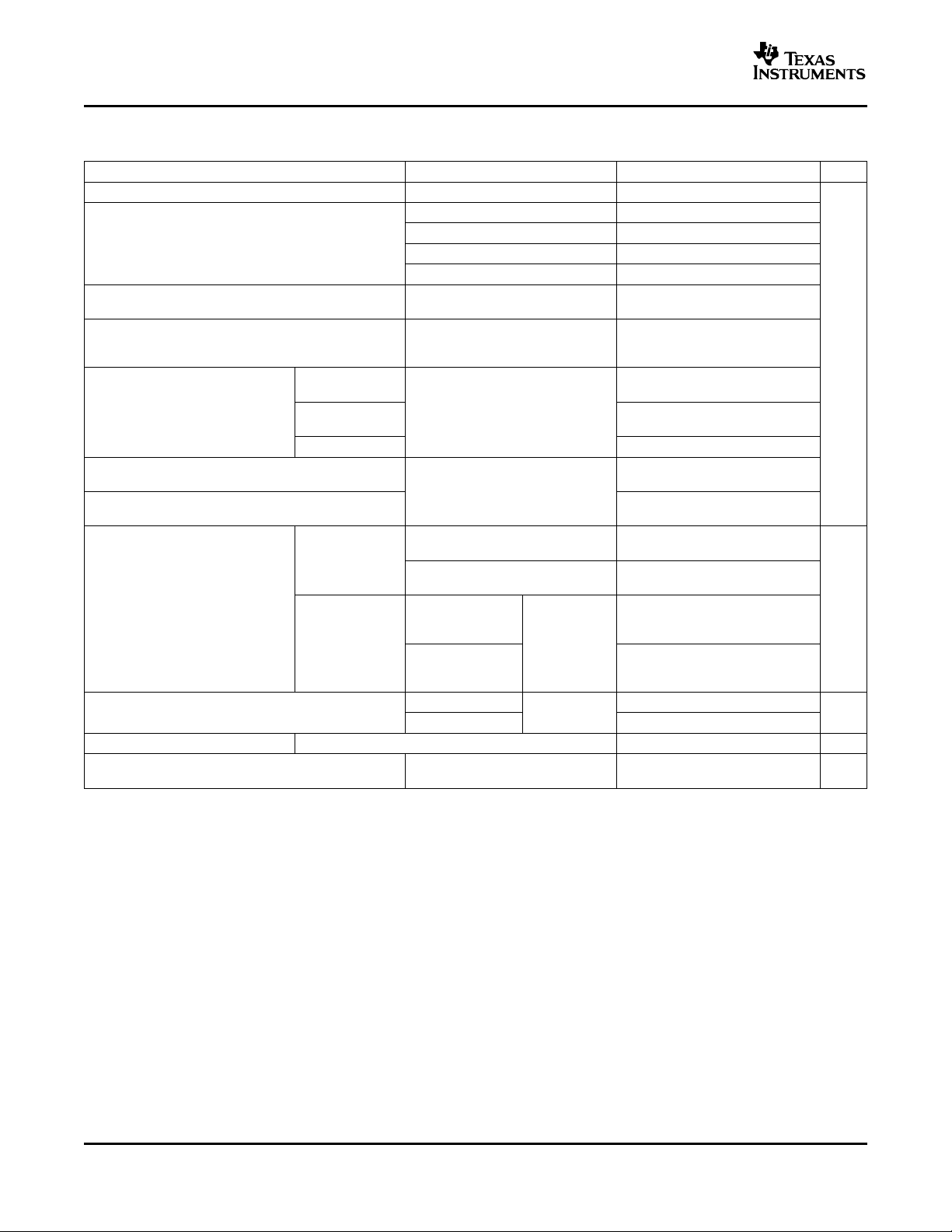
DRIVER ELECTRICAL CHARACTERISTICS
over recommended operating conditions unless otherwise noted
PARAMETER TEST CONDITIONS MIN TYP
V
I(K)
|V
OD(SS)
∆ |V
OD(SS)
V
OD(RING)
V
OC(PP)
V
OC(SS)
∆ V
OC(SS)
I
or I
Z(Z)
I
or I
Z(S)
I
I
C
(OD)
(1) All typical values are at 25 ° C and with a 5-V supply.
Input clamp voltage II= –18 mA –1.5
| Steady-state differential output voltage
Change in magnitude of steady-state RL= 54 Ω , See Figure 1 and
| –0.2 0.2
differential output voltage between states Figure 2
Differential Output Voltage overshoot
and undershoot
HVD50, HVD53,
Peak-to-peak
HVD56, HVD58
common-mode HVD51, HVD54, See Figure 4
output voltage HVD57, HVD59
HVD52, HVD55 0.4
Steady-state common-mode
output voltage
Change in steady-state common-mode
output voltage
High-impedance state
Y(Z)
output current
HVD53, HVD54,
HVD55, HVD58,
HVD59
Short Circuit output Current mA
Y(S)
Input current D, DE 0 100 µA
Differential output capacitance 16 pF
(1)
IO= 0 4 V
RL= 54 Ω , See Figure 1 (RS-485) 1.7 2.6
RL= 100 Ω , See Figure 1 (RS-422) 2.4 3.2
V
= –7 V to 12 V, See Figure 2 1.6
test
RL= 54 Ω , CL= 50 pF, See
Figure 5 0.05 |V
See Figure 3 for definition
0.5
0.4
2.2 3.3
See Figure 4
–0.1 0.1
V
= 0 V, VZor VY= 12 V,
CC
Other input at 0 V
V
= 0 V, VZor VY= –7 V,
CC
Other input at 0 V
V
= 5 V or 0 V,
CC
DE = 0 V 90
VZor VY= 12 V
V
= 5 V or 0 V,
CC
DE = 0 V –10
Other input
at 0 V
–10
VZor VY= –7 V
VZor VY= –7 V –250 250
VZor VY= 12 V –250 250
V
= 0.4 sin (4E6 π t) + 0.5 V,
OD
DE at 0 V
Other input
at 0 V
MAX UNIT
CC
|
OD(SS)
V
90
µ A
4
www.ti.com
DRIVER SWITCHING CHARACTERISTICS
over recommended operating conditions unless otherwise noted
PARAMETER TEST CONDITIONS MIN TYP
t
PLH
t
PHL
t
r
t
f
t
sk(p)
t
sk(pp)
Propagation delay time,
low-to-high-level output
Propagation delay time,
high-to-low-level output
Differential output signal
rise time
Differential output signal fall
time
Pulse skew (|t
(2)
Part-to-part skew HVD51, HVD54, HVD57, HVD59 4 ns
- t
PHL
PLH
Propagation delay time,
t
PZH1
high-impedance-to-high- HVD54, HVD59 180 ns
level output
Propagation delay time,
t
PHZ
high-level-to-high- HVD54, HVD59 40 ns
impedance output
Propagation delay time,
t
PZL1
high-impedance-to-low-level HVD54, HVD59 200 ns
output
Propagation delay time,
t
PLZ
t
PZH2
t
PZL2
low-level-to-high-impedance HVD54, HVD59 70 ns
output
Propagation delay time, standby-to-high-level output 3300 ns
Propagation delay time, standby-to-low-level output 3300 ns
(1) All typical values are at 25°C and with a 5-V supply.
(2) t
is the magnitude of the difference in propagation delay times between any specified terminals of two devices when both devices
sk(pp)
operate with the same supply voltages, at the same temperature, and have identical packages and test circuits.
HVD50, HVD53, HVD56, HVD58 4 8 12
HVD51, HVD54, HVD57, HVD59 20 29 46 ns
HVD52, HVD55 90 143 230
HVD50, HVD53, HVD56, HVD58 4 8 12
HVD51, HVD54, HVD57, HVD59 20 30 46 ns
HVD52, HVD55 90 143 230
HVD50, HVD53, HVD56, HVD58 3 6 12
HVD51, HVD54, HVD57, HVD59 25 34 60 ns
HVD52, HVD55 130 197 300
HVD50, HVD53, HVD56, HVD58 3 6 11
RL= 54 Ω , CL= 50 pF,
See Figure 5
HVD51, HVD54, HVD57, HVD59 25 33 60 ns
HVD52, HVD55 130 192 300
HVD50, HVD53, HVD56, HVD58 2
|) HVD51, HVD54, HVD57, HVD59 2 ns
HVD52, HVD55 8
HVD50, HVD53, HVD56, HVD58 1
HVD52, HVD55 22
HVD53, HVD58 30
HVD55 380
HVD53, HVD58 16
RL= 110 Ω , RE at 0 V,
See Figure 6
D = 3 V and S1 = Y,
D = 0 V and S1 = Z
HVD55 110
HVD53, HVD58 23
HVD55 420
HVD53, HVD58 19
RL= 110 Ω , RE at 0 V,
See Figure 7
D = 3 V and S1 = Z,
D = 0 V and S1 = Y
HVD55 160
RL= 110 Ω , RE at 3 V,
See Figure 6
D = 3 V and S1 = Y,
D = 0 V and S1 = Z
RL= 110 Ω , RE at 3 V,
See Figure 7
D = 3 V and S1 = Z,
D = 0 V and S1 = Y
SN65HVD50-SN65HVD55
SN65HVD56-SN65HVD59
SLLS666 – SEPTEMBER 2005
(1)
MAX UNIT
5
www.ti.com
SN65HVD50-SN65HVD55
SN65HVD56-SN65HVD59
SLLS666 – SEPTEMBER 2005
RECEIVER ELECTRICAL CHARACTERISTICS
over recommended operating conditions unless otherwise noted
PARAMETER TEST CONDITIONS MIN TYP
V
IT+
V
IT-
V
hys
V
IK
V
O
I
O(Z)
IAor I
I
IH
C
ID
I
CC
(1) All typical values are at 25°C and with a 5-V supply.
Positive-going differential input
threshold voltage
Negative-going differential input
threshold voltage
Hysteresis voltage (V
- V
IT+
IT-
IO= –8 mA –0.02
IO= 8 mA –0.20
) 50 mV
Enable-input clamp voltage II= –18 mA –1.5 V
Output voltage V
High-impedance-state output
current
HVD50,
HVD53, Other input
HVD56, at 0 V
HVD58
Bus input current
B
HVD51, VAor VB= 12 V 0.05 0.10
HVD52,
HVD54, Other input
HVD55, at 0 V
HVD57,
HVD59
Input current, RE
VID= 200 mV, IO= –8 mA, See Figure 8 4.0
VID= –200 mV, IO= 8 mA, See Figure 8 0.3
VO= 0 or VCCRE at V
VAor VB= 12 V 0.19 0.3
VAor VB= 12 V, V
VAor VB= -7 V –0.35 –0.19
VAor VB= -7 V, V
VAor VB= 12 V, V
VAor VB= -7 V –0.10 –0.05
VAor VB= -7 V, V
VIH= 2 V –60 µA
VIL= 0.8 V –60 µA
Differential input capacitance VID= 0.4 sin (4E6 π t) + 0.5 V, DE at 0 V 16 pF
HVD50,
HVD51, 8.0
HVD52
D at 0 V or V
HVD56,
HVD57
HVD53 2.3
HVD54, RE at 0 V, D at 0 V or VCC, DE at 0 V,
HVD55 No load (Receiver enabled and
HVD58,
driver disabled)
HVD59
HVD53,
HVD54, RE at VCC, D at VCC, DE at 0 V,
Supply current
HVD55, No load (Receiver disabled and 0.08 1 µA
HVD58, driver disabled)
HVD59
HVD53 2.7
HVD54,
HVD55
HVD58 4.3
RE at 0 V, D at 0 V or VCC, DE at VCC,
No load (Receiver enabled and
driver enabled)
HVD59 9.7
HVD53 2.3
HVD54,
HVD55
HVD58 3.2
RE at VCC, D at 0 V or VCC, DE at V
No load (Receiver disabled and
driver enabled)
HVD59 8.5
CC
= 0 V 0.24 0.4
CC
= 0 V –0.25 –0.14
CC
= 0 V 0.06 0.10
CC
= 0 V –0.10 –0.03
CC
and No Load
CC
CC
(1)
MAX UNIT
–1 1 µA
9.5
2.9
4.5
8.0
7.7
V
mA
mA
mA
mA
6
www.ti.com
RECEIVER SWITCHING CHARACTERISTICS
over recommended operating conditions unless otherwise noted
PARAMETER TEST CONDITIONS MIN TYP
t
PLH
t
PHL
t
sk(p)
t
sk(pp)
t
r
t
f
t
PHZ
t
PZH1
t
PZH2
t
PLZ
t
PZL1
t
PZL2
Propagation delay time,
low-to-high-level output
Propagation delay time,
high-to-low-level output
Pulse skew (|t
(2)
Part-to-part skew HVD51, HVD54, HVD57, HVD59 6
- t
PHL
|)
PLH
Output signal rise time 2.3 4
Output signal fall time 2.4 4
Output disable time from high level 17
Output enable time to high level 10
Propagation delay time, standby-to-high-level output 3300
Output disable time from low level 13
Output enable time to low level 10
Propagation delay time, standby-to-low-level output 3300
(1) All typical values are at 25°C and with a 5-V supply
(2) .t
is the magnitude of the difference in propagation delay times between any specified terminals of two devices when both devices
sk(pp)
operate with the same supply voltages, at the same temperature, and have identical packages and test circuits.
HVD50, HVD53, HVD56, HVD58 24 40
HVD51, HVD52, HVD54, HVD55,
HVD57, HVD59
HVD50, HVD53, HVD56, HVD58 26 35
HVD51, HVD52, HVD54, HVD55,
HVD57, HVD59
HVD50, HVD53, HVD56, HVD57,
HVD58, HVD59
HVD51, HVD54, HVD52, HVD55 7
VID= -1.5 V to 1.5 V,
CL= 15 pF,
See Figure 9
HVD50, HVD53, HVD56, HVD58 5
HVD52, HVD55 6
DE at 3 V, CL= 15 pF
See Figure 10
DE at 0 V, CL= 15 pF
See Figure 10
DE at 3 V, CL= 15 pF
See Figure 11
DE at 0 V, CL= 15 pF
See Figure 11
SN65HVD50-SN65HVD55
SN65HVD56-SN65HVD59
SLLS666 – SEPTEMBER 2005
(1)
MAX UNIT
43 55
47 60
5
ns
7

www.ti.com
SN65HVD50-SN65HVD55
SN65HVD56-SN65HVD59
SLLS666 – SEPTEMBER 2005
RECEIVER EQUALIZATION CHARACTERISTICS
over recommended operating conditions unless otherwise noted
PARAMETER TEST CONDITIONS MIN TYP
25 Mbps HVD53 PREVIEW
Peak-to-peak
t
eye-pattern HVD56, HVD58 PREVIEW
j(pp)
jitter
(1) The HVD53 and HVD54 do not have receiver equalization but are specified for comparison.
(2) All typical values are at V
Pseudo-random NRZ
code with a bit pattern
length o 216-1, Belden
3105A cable
= 5 V, and temperature = 25 ° C.
CC
10 Mbps 250 m
5 Mbps 500 m
3 Mbps 500 m
1 Mbps 1000 m
(1)
0 m HVD56, HVD58 PREVIEW ns
100 m
150 m
200 m
200 m
300 m
HVD53 PREVIEW
HVD56, HVD58 PREVIEW
HVD56, HVD58 PREVIEW
HVD53 PREVIEW
HVD56, HVD58 PREVIEW
HVD53 PREVIEW
HVD56, HVD58 PREVIEW
HVD53 PREVIEW
HVD53 PREVIEW
HVD56, HVD58 PREVIEW
HVD54 PREVIEW
HVD57, HVD59 PREVIEW
HVD53 PREVIEW
HVD54 PREVIEW
HVD56, HVD58 PREVIEW
HVD57, HVD59 PREVIEW
HVD54 PREVIEW
HVD57, HVD59 PREVIEW
(2)
MAX UNIT
8

www.ti.com
60 Ω ±1%
V
OD
0 or 3 V
_
+
−7 V < V
(test)
< 12 V
DE
V
CC
Y
Z
D
375 Ω ±1%
375 Ω ±1%
I
Y
V
OD R
L
0 or 3 V
V
Y
V
Z
I
Z
DE
V
CC
I
I
V
I
Y
Z
SN65HVD50-SN65HVD55
SN65HVD56-SN65HVD59
THERMAL CHARACTERISTICS
over operating free-air temperature range unless otherwise noted
PARAMETER TEST CONDITIONS MIN TYP MAX UNIT
Junction–to–ambient
thermal resistance
θ
JA
Junction–to–ambient
thermal resistance
Junction–to–board
θ
JB
thermal resistance
Junction–to–case
θ
JC
thermal resistance
Low-K board
(2)
High-K board
(2)
High-K board
No board
RL= 60 Ω , CL= 50 pF, HVD50, HVD56 (25Mbps) 420
Input to D a 50% duty cycle
square wave at indicated
Device power
P
D
dissipation
signaling rate
RL= 60 Ω , CL= 50 pF, HVD53, HVD58 (25Mbps) 420
DE at VCCRE at 0 V,
Input to D a 50% duty cycle
square wave at indicated
signaling rate
Low-K board, No airflow HVD50, HVD56 –40 55
Ambient air
T
A
temperature
High-K board, No airflow HVD50, HVD51, HVD52, HVD56, HVD57 –40 85
T
Thermal shutdown junction temperature 165
JSD
(3)
, No airflow HVD50, HVD51, HVD52, HVD56, HVD57 230.8
HVD53, HVD54, HVD55, HVD58, HVD59 162.6
(4)
, No airflow HVD50, HVD51, HVD52, HVD56, HVD57 135.1
HVD53, HVD54, HVD55, HVD58, HVD59 92.1
HVD50, HVD51, HVD52, HVD56, HVD57 44.4
HVD53, HVD54, HVD55, HVD58, HVD59 61.1
HVD50, HVD51, HVD52, HVD56, HVD57 43.5
HVD53, HVD54, HVD55, HVD58, HVD59 58.6
HVD51, HVD57 (10Mbps) 404
HVD52 (1Mbps) 383
HVD54, HVD59 (10Mbps) 404
HVD55 (1Mbps) 383
HVD51, HVD52, HVD57 –40 84
HVD53, HVD54, HVD55, HVD58, HVD59 –40 85
HVD53, HVD54, HVD55, HVD58, HVD59 –40 85
(1)
SLLS666 – SEPTEMBER 2005
° C/W
mW
° C
(1) See Application Information section for an explanation of these parameters.
(2) The intent of θJAspecification is solely for a thermal performance comparison of one package to another in a standardized environment.
This methodology is not meant to and will not predict the performance of a package in an application-specific environment.
(3) In accordance with the Low-K thermal metric definitions of EIA/JESD51-3.
(4) In accordance with the High-K thermal metric definitions of EIA/JESD51-7.
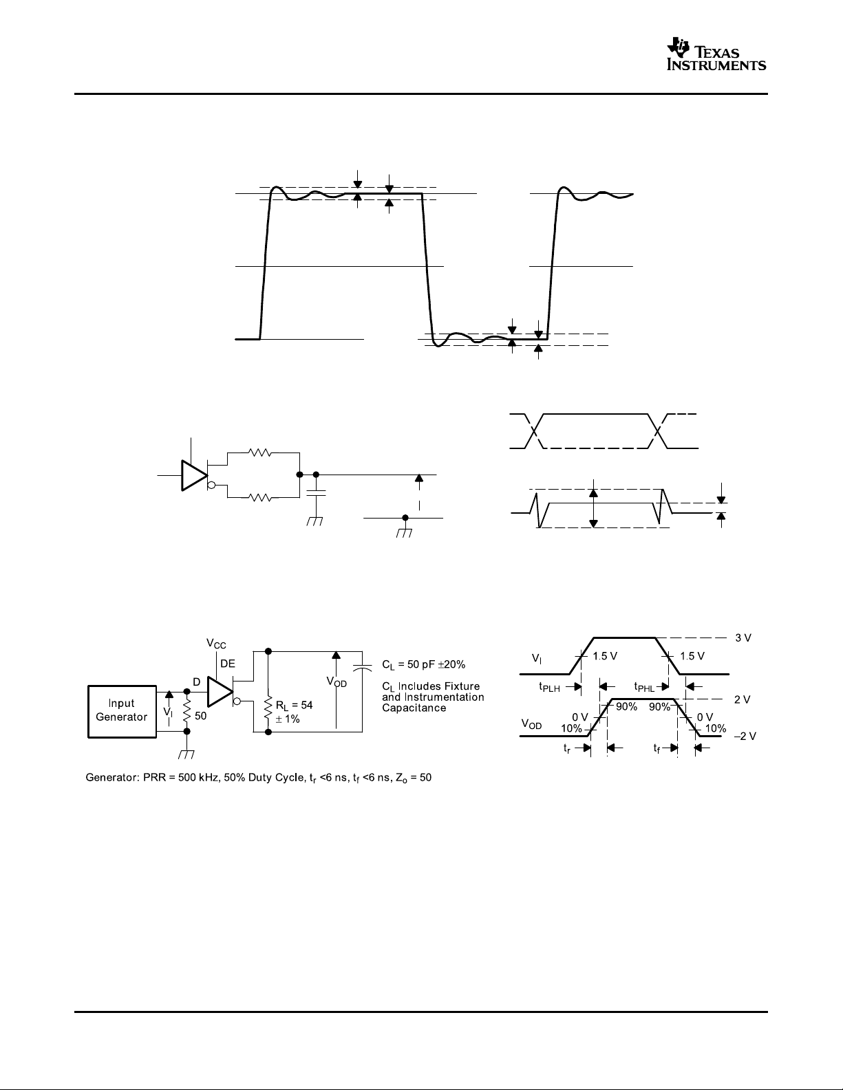
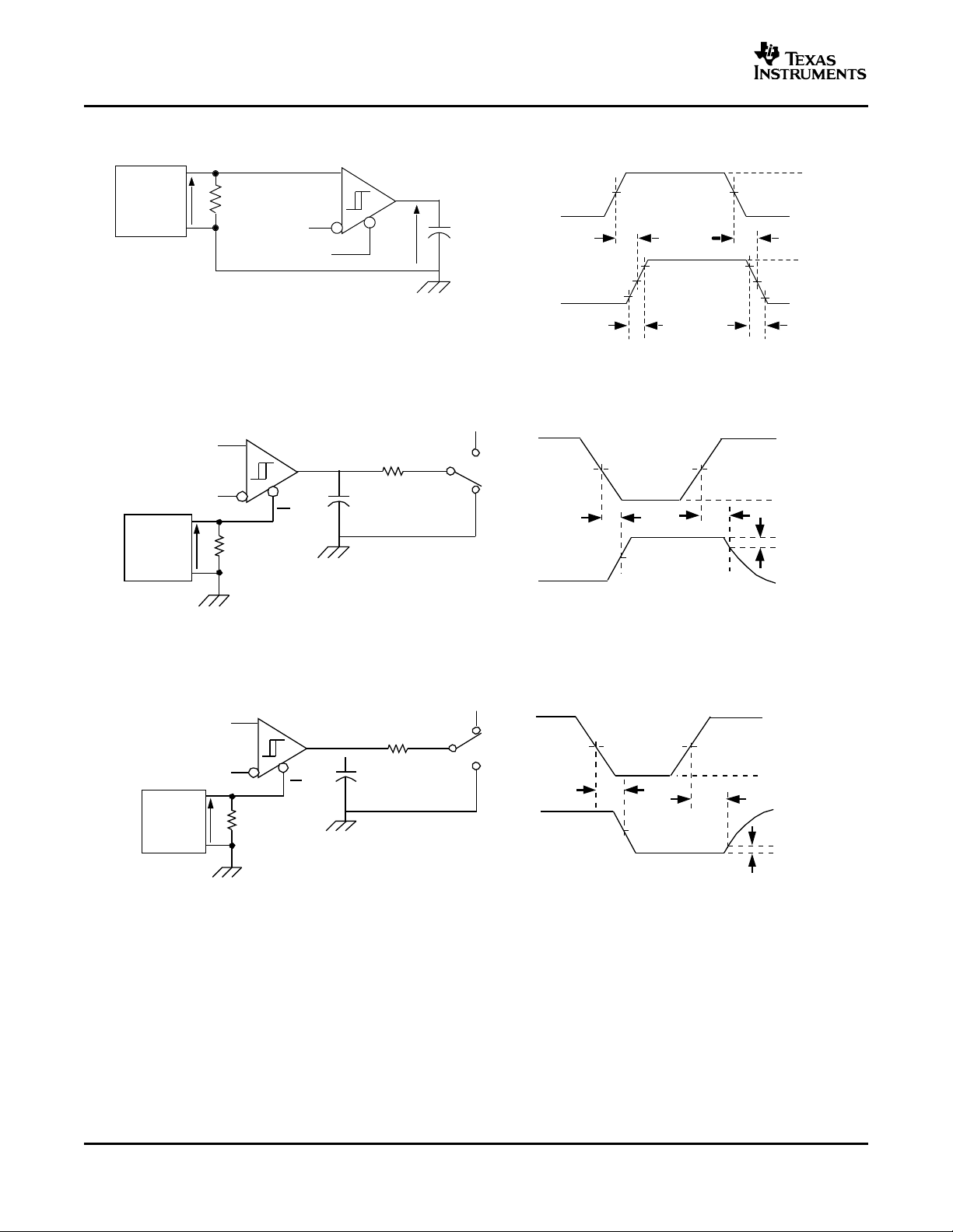
PARAMETER MEASUREMENT INFORMATION
Figure 1. Driver V
Test Circuit: Voltage and Current Figure 2. Driver V
OD
Definitions Circuit
With Common-Mode Loading Test
OD
9
www.ti.com
V
OD(RING)
V
OD(RING)
-V
OD(SS)
V
OD(SS)
0 V Differential
V
OC
27 Ω ± 1%
Input
Y
Z
V
Y
V
Z
V
OC(PP)
∆V
OC(SS)
V
OC
27 Ω ± 1%
CL= 50 pF ±20%
D
Y
Z
DE
V
CC
Input: PRR = 500 kHz, 50% Duty Cycle,tr<6ns, tf<6ns, ZO= 50 Ω
C
L
Includes Fixture and
Instrumentation Capacitance
Y
Z
W
W
W
»
»
SN65HVD50-SN65HVD55
SN65HVD56-SN65HVD59
SLLS666 – SEPTEMBER 2005
PARAMETER MEASUREMENT INFORMATION (continued)
VOD(RING) is measured at four points on the output waveform, corresponding to overshoot and undershoot from
theVOD(H) and VOD(L) steady state values.
Figure 3. V
OD(RING)
Waveform and Definitions
Figure 4. Test Circuit and Definitions for the Driver Common-Mode Output Voltage
Figure 5. Driver Switching Test Circuit and Voltage Waveforms
10

www.ti.com
V
I
V
O
t
PZH(1 & 2)
50 W
D
D S1
3 V Y
0 V Z
Y
Z
V
I
RL= 110 W
±1%
CL= 50 pF
±20%
V
O
Generator: PRR = 500kHz, 50% Duty Cycle, tr<6 ns, tf< 6ns, Z0= 50 W
CLIncludes Fixture and Instrumentation Capacitance
3 V
1.5 V
1.5 V
t
PHZ
2.3 V
DE
Input
Generator
~ 0 V
V
OH
0.5 V
0 V
S1
Input
Generator
50 Ω
V
O
S1
V
CC
3 V
V
CC
1.5 V 1.5 V
t
PZL(1&2)
t
PLZ
2.3 V
0.5 V
0 V
V
OL
V
I
V
O
Generator: PRR = 500 kHz, 50% Duty Cycle, tr<6 ns, tf<6 ns, Zo= 50 Ω
R
L
= 110 Ω
± 1%
C
L
= 50 pF ±20%
CLIncludes Fixture
and Instrumentation
Capacitance
D
Y
Z
DE
V
I
D S1
3 V Z
0 V Y
B
A
R
I
O
V
ID
I
A
I
B
V
O
V
B
V
IC
V
A
VA+ V
B
2
I
I
RE
V
I
PARAMETER MEASUREMENT INFORMATION (continued)
Figure 6. Driver High-Level Output Enable and Disable Time Test Circuit and Voltage Waveforms
SN65HVD50-SN65HVD55
SN65HVD56-SN65HVD59
SLLS666 – SEPTEMBER 2005
Figure 7. Driver Low-Level Output Enable and Disable Time Test Circuit and Voltage Waveforms
Figure 8. Receiver Voltage and Current Definitions
11
www.ti.com
B
A
R
V
O
V
I
V
O
t
PLH
t
PHL
50 W
V
I
Input
Generator
C = 15 pF
±20%
L
CLIncludes Fixture
and Instrumentation
Capacitance
Generator : PRR = 500 kHz , 50%
Duty Cycle , t < 6 ns , t < 6ns ,
Z = 50
W
3 V
1 .5 V1 .5 V
V
OH
V
OL
t
r
t
f
90 % 90 %
10%
1.5 V
1.5 V
10%
1.5 V
0 V
RE
0 V
B
A
RVO
50 W
V
I
Input
Generator
CL= 15 pF
±20%
CLIncludes Fixture and
Instrumentation Capacitance
S1
1 k ±1%W
A
B
V
CC
V
I
t
PZH(1 & 2)
3 V
1.5 V
1.5 V
PHZ
0 V
V
O
1.5 V
~0 V
V
OH
0.5 V
1.5 V
0 V
Generator: P = 500 kHz, 50%, Duty Cycle, t < 6 ns, t < 6 ns, Z = 50
RR r f 0
W
B
A
R
V
O
50 W
V
I
Input
Generator
CL= 15 pF
±20%
C
L
Includes Fixture
and Instrumentation
Capacitance
Generator: P = 500 kHz, 50%, Duty Cycle, t < 6 ns, t < 6 ns, Z = 50
RR r f 0
W
RE
S1
1 k ±1%W
A
B
V
CC
V
I
V
O
3 V
1.5 V
1.5 V
V
CC
V
OL
0.5 V
0 V
1.5 V
t
PZL(1 & 2)
t
PLZ
0 V
1.5 V
SN65HVD50-SN65HVD55
SN65HVD56-SN65HVD59
SLLS666 – SEPTEMBER 2005
PARAMETER MEASUREMENT INFORMATION (continued)
Figure 9. Receiver Switching Test Circuit and Voltage Waveforms
Figure 10. Receiver High-Level Enable and Disable Time Test Circuit and Voltage Waveforms
Figure 11. Receiver Low-Level Enable and Disable Time Test Circuit and Voltage Waveforms
12
www.ti.com
B
A
R
100 W
±1%
+
-
Pulse Generator
15 ms duration
1% Duty Cycle
t , t 100 ns
r f
£
Z
Y
D
100 W
±1%
+
-
DE
0 V or 3 V
0 V or 3 V
RE
4
5
9
10
Y
Z
D
DE
A
B
12
11
2
R
3
RE
Low
Shutdown
-Power
SN65HVD50-SN65HVD55
SN65HVD56-SN65HVD59
SLLS666 – SEPTEMBER 2005
PARAMETER MEASUREMENT INFORMATION (continued)
Figure 12. Test Circuit, Transient Overvoltage Test
DEVICE INFORMATION
LOW-POWER SHUTDOWN MODE
When both the driver and receiver are disabled (DE low and RE high) the device is in shutdown mode. If the
enable inputs are in this state for less than 60 ns, the device does not enter shutdown mode. This guards against
inadvertently entering shutdown mode during driver/receiver enabling. Only when the enable inputs are held in
this state for 300 ns or more, the device is assured to be in shutdown mode. In this low-power shutdown mode,
most internal circuitry is powered down, and the supply current is typically less than 1 nA. When either the driver
or the receiver is re-enabled, the internal circuitry becomes active.
Figure 13. Low-Power Shutdown Logic Diagram
If only the driver is re-enabled (DE transitions to high) the driver outputs are driven according to the D input after
the enable times given by t
and t
PZH2
in the driver switching characteristics. If the D input is open when the
PZL2
driver is enabled, the driver outputs defaults to A high and B low, in accordance with the driver failsafe feature.
If only the receiver is re-enabled ( RE transitions to low) the receiver output is driven according to the state of the
bus inputs (A and B) after the enable times given by t
and t
PZH2
in the receiver switching characteristics. If
PZL2
there is no valid state on the bus the receiver responds as described in the failsafe operation section.
If both the receiver and driver are re-enabled simultaneously, the receiver output is driven according to the state
of the bus inputs (A and B) and the driver output is driven according to the D input. Note that the state of the
active driver affects the inputs to the receiver. Therefore, the receiver outputs are valid as soon as the driver
outputs are valid.
13

www.ti.com
SN65HVD50-SN65HVD55
SN65HVD56-SN65HVD59
SLLS666 – SEPTEMBER 2005
DEVICE INFORMATION (continued)
FUNCTION TABLES
SN65HVD53, SN65HVD54, SN65HVD55, SN65HVD58,
SN65HVD59 DRIVER
INPUTS OUTPUTS
D DE Y Z
H H H L
L H L H
X L or open Z Z
Open H L H
SN65HVD53, SN65HVD54, SN65HVD55, SN65HVD58,
SN65HVD59 RECEIVER
DIFFERENTIAL INPUTS ENABLE OUTPUT
VID= VA- V
VID≤ –0.2 V L L
–0.2 V < VID< –0.02 V L ?
–0.02 V ≤ V
Open Circuit L H
Idle circuit L H
Short Circuit, VA= V
B
ID
X H or open Z
B
RE R
L H
L H
SN65HVD50, SN65HVD51, SN65HVD52, SN65HVD56,
SN65HVD57 DRIVER
OUTPUTS
INPUT Y Z
D
H H L
L L H
Open L H
SN65HVD50, SN65HVD51, SN65HVD52, SN65HVD56,
SN65HVD57 RECEIVER
DIFFERENTIAL INPUTS OUTPUT
VID= VA- V
VID≤ –0.2 V L
–0.2 V < VID< –0.02 V ?
–0.02 V ≤ V
Open Circuit H
Idle circuit H
Short Circuit, VA= V
B
ID
B
R
H
H
14

www.ti.com
EQUIVALENT INPUT AND OUTPUT SCHEMATIC DIAGRAMS
V
CC
Input
470 W
130 kW
V
CC
5 W
Output
R Output
9 V
9 V
R3
22 V
22 V
Input
R2
R1
V
CC
A Input
R3
22 V
22 V
Input
R2
R1
V
CC
B Input
16 V
16 V
Y and Z Outputs
Output
V
CC
RE Input
V
CC
Input
470 W
125 kW
9 V
D and DE Input
SN65HVD50-SN65HVD55
SN65HVD56-SN65HVD59
SLLS666 – SEPTEMBER 2005
SN65HVD50, SN65HVD53, SN65HVD56, SN65HVD58 9 k Ω 45 k Ω
SN65HVD51, SN65HVD52, SN65HVD54, SN65HVD55 SN65HVD57, 36 k Ω 180 k Ω
SN65HVD58, SN65HVD59
R1/R2 R3
15

www.ti.com
40
45
50
55
60
65
70
0 1 2 3 4 5
Signaling Rate (Mbps)
I (RMS Supply Current, mA)
CC
T =25°C R = 54
= V C = 50 pF
DE = V
A L
CC L
CC
W
RE
V = 5.0 VDC
CC
40
45
50
55
60
65
70
0 5 10 15 20 25
Signaling Rate (Mbps)
I (RMS Supply Current, mA)
CC
T =25°C R = 54
R = V C = 50 pF
DE = V
A L
E CC L
CC
W
V = 5.0 VDC
CC
40
45
50
55
60
65
70
75
0 0.2 0.4 0.6 0.8 1
Signaling Rate (Mbps)
I (RMS Supply Current, mA)
CC
T =25°C R = 54
= V C = 50 pF
DE = V
A L
CC L
CC
W
RE
V = 5.0 VDC
CC
SN65HVD50-SN65HVD55
SN65HVD56-SN65HVD59
SLLS666 – SEPTEMBER 2005
TYPICAL CHARACTERISTICS
HVD50, HVD53 HVD51, HVD54
RMS Supply Current RMS Supply Current
vs vs
Signaling Rate Signaling Rate
16
Figure 14. Figure 15.
HVD52, HVD55
RMS Supply Current
vs
Signaling Rate
Figure 16.

www.ti.com
-60
-40
-20
0
20
40
60
-7 -4 -1 2 5 8 11 14
V - Bus Input Voltage - V
I
I - Bus Input Current - µA
I
T = 25°C
= 0 V
DE = 0 V
A
RE
V = 5 V
CC
-250
-200
-150
-100
-50
0
50
100
150
200
250
-7 -4 -1 2 5 8 11 14
V - Bus Input Voltage - V
I
I - Bus Input Current - µA
I
T = 25°C
= 0 V
DE = 0 V
A
RE
V = 5 V
CC
-0.02
0
0.02
0.04
0.06
0.08
0.1
0.12
0 1 2 3 4 5
V - Low-Level Output Voltage - V
OL
I - Low-level Output Current - A
OL
VCC = 5 V
DE = V
D = 0 V
CC
-0.13
-0.11
-0.09
-0.07
-0.05
-0.03
-0.01
0.01
0 1 2 3 4 5
V - High-Level Output Voltage - V
OH
I - High-level Output Current - A
OH
VCC = 5 V
DE = V
D = 0 V
CC
TYPICAL CHARACTERISTICS (continued)
SN65HVD50-SN65HVD55
SN65HVD56-SN65HVD59
SLLS666 – SEPTEMBER 2005
HVD50, HVD53 HVD51, HVD52, HVD54, HVD55
Bus Input Current Bus Input Current
vs vs
Input Voltage Input Voltage
Driver Low-Level Output Current Driver High-Level Output Current
Low-Level Output Voltage High-Level Output Voltage
Figure 17. Figure 18.
vs vs
Figure 19. Figure 20.
17

www.ti.com
2.4
2.5
2.6
2.7
2.8
2.9
-40 -15 10 35 60 85
T - Free-Air Temperature - °C
A
V - Driver Differential Voltage - V
OD
V = 5 V
DE at V
D at V
CC
CC
CC
0
10
20
30
40
50
60
0 1 2 3 4 5 6
V - Supply Voltage - V)
CC
I - Driver Output Current - mA
O
T = 25°C
R = 54
D = V
DE = V
A
L
CC
CC
W
V = 5 V
CC
SN65HVD50-SN65HVD55
SN65HVD56-SN65HVD59
SLLS666 – SEPTEMBER 2005
TYPICAL CHARACTERISTICS (continued)
Driver Differential Output Voltage Driver Output Current
vs vs
Free-Air Temperature Supply Voltage
Figure 21. Figure 22.
18

www.ti.com
SN65HVD50-SN65HVD55
SN65HVD56-SN65HVD59
SLLS666 – SEPTEMBER 2005
APPLICATION INFORMATION
THERMAL CHARACTERISTICS OF IC PACKAGES
θ
(Junction-to-Ambient Thermal Resistance) is defined as the difference in junction temperature to ambient
JA
temperature divided by the operating power.
θ
is not a constant and is a strong function of:
JA
• the PCB design (50% variation)
• altitude (20% variation)
• device power (5% variation)
θ
can be used to compare the thermal performance of packages if the specific test conditions are defined and
JA
used. Standardized testing includes specification of PCB construction, test chamber volume, sensor locations,
and the thermal characteristics of holding fixtures. θ
temperatures for other installations.
TI uses two test PCBs as defined by JEDEC specifications. The low-k board gives average in-use condition
thermal performance, and it consists of a single copper trace layer 25 mm long and 2-oz thick. The high-k board
gives best case in-use condition, and it consists of two 1-oz buried power planes with a single copper trace layer
25 mm long and 2-oz thick. A 4% to 50% difference in θ
θ
(Junction-to-Case Thermal Resistance) is defined as difference in junction temperature to case divided by
JC
the operating power. It is measured by putting the mounted package up against a copper block cold plate to
force heat to flow from die, through the mold compound into the copper block.
θ
is a useful thermal characteristic when a heatsink applied to package. It is not a useful characteristic to
JC
predict junction temperature because it provides pessimistic numbers if the case temperature is measured in a
nonstandard system and junction temperatures are backed out. It can be used with θ
simulation of a package system.
θ
(Junction-to-Board Thermal Resistance) is defined as the difference in the junction temperature and the
JB
PCB temperature at the center of the package (closest to the die) when the PCB is clamped in a cold-plate
structure. θ
θ
provides an overall thermal resistance between the die and the PCB. It includes a bit of the PCB thermal
JB
is only defined for the high-k test card.
JB
resistance (especially for BGA’s with thermal balls) and can be used for simple 1-dimensional network analysis of
package system, see Figure 23 .
is often misused when it is used to calculate junction
JA
can be measured between these two test cards
JA
in 1-dimensional thermal
JB
Figure 23. Thermal Resistance
19
PACKAGE OPTION ADDENDUM
www.ti.com
26-Sep-2005
PACKAGING INFORMATION
Orderable Device Status
(1)
Package
Type
Package
Drawing
Pins Package
Qty
Eco Plan
SN65HVD53D PREVIEW SOIC D 14 50 TBD Call TI Call TI
SN65HVD53DR PREVIEW SOIC D 14 2500 TBD Call TI Call TI
SN65HVD54D PREVIEW SOIC D 14 50 TBD Call TI Call TI
SN65HVD54DR PREVIEW SOIC D 14 2500 TBD Call TI Call TI
SN65HVD55D PREVIEW SOIC D 14 50 TBD Call TI Call TI
SN65HVD55DR PREVIEW SOIC D 14 2500 TBD Call TI Call TI
(1)
The marketing status values are defined as follows:
ACTIVE: Product device recommended for new designs.
LIFEBUY: TI has announced that the device will be discontinued, and a lifetime-buy period is in effect.
NRND: Not recommended for new designs. Device is in production to support existing customers, but TI does not recommend using this part in
a new design.
PREVIEW: Device has been announced but is not in production. Samples may or may not be available.
OBSOLETE: TI has discontinued the production of the device.
(2)
Eco Plan - The planned eco-friendly classification: Pb-Free (RoHS) or Green (RoHS & no Sb/Br) - please check
http://www.ti.com/productcontent for the latest availability information and additional product content details.
TBD: The Pb-Free/Green conversion plan has not been defined.
Pb-Free (RoHS): TI's terms "Lead-Free" or "Pb-Free" mean semiconductor products that are compatible with the current RoHS requirements
for all 6 substances, including the requirement that lead not exceed 0.1% by weight in homogeneous materials. Where designed to be soldered
at high temperatures, TI Pb-Free products are suitable for use in specified lead-free processes.
Green (RoHS & no Sb/Br): TI defines "Green" to mean Pb-Free (RoHS compatible), and free of Bromine (Br) and Antimony (Sb) based flame
retardants (Br or Sb do not exceed 0.1% by weight in homogeneous material)
(2)
Lead/Ball Finish MSL Peak Temp
(3)
(3)
MSL, Peak Temp. -- The Moisture Sensitivity Level rating according to the JEDEC industry standard classifications, and peak solder
temperature.
Important Information and Disclaimer:The information provided on this page represents TI's knowledge and belief as of the date that it is
provided. TI bases its knowledge and belief on information provided by third parties, and makes no representation or warranty as to the
accuracy of such information. Efforts are underway to better integrate information from third parties. TI has taken and continues to take
reasonable steps to provide representative and accurate information but may not have conducted destructive testing or chemical analysis on
incoming materials and chemicals. TI and TI suppliers consider certain information to be proprietary, and thus CAS numbers and other limited
information may not be available for release.
In no event shall TI's liability arising out of such information exceed the total purchase price of the TI part(s) at issue in this document sold by TI
to Customer on an annual basis.
Addendum-Page 1

PACKAGE OPTION ADDENDUM
www.ti.com
17-Nov-2005
PACKAGING INFORMATION
Orderable Device Status
(1)
Package
Type
Package
Drawing
Pins Package
Qty
Eco Plan
SN65HVD53D ACTIVE SOIC D 14 50 Green (RoHS &
no Sb/Br)
SN65HVD53DG4 ACTIVE SOIC D 14 50 Green (RoHS &
no Sb/Br)
SN65HVD53DR ACTIVE SOIC D 14 2500 Green (RoHS &
no Sb/Br)
SN65HVD53DRG4 ACTIVE SOIC D 14 2500 Green (RoHS &
no Sb/Br)
SN65HVD54D ACTIVE SOIC D 14 50 Green (RoHS &
no Sb/Br)
SN65HVD54DG4 ACTIVE SOIC D 14 50 Green (RoHS &
no Sb/Br)
SN65HVD54DR ACTIVE SOIC D 14 2500 Green (RoHS &
no Sb/Br)
SN65HVD54DRG4 ACTIVE SOIC D 14 2500 Green (RoHS &
no Sb/Br)
SN65HVD55D ACTIVE SOIC D 14 50 Green (RoHS &
no Sb/Br)
SN65HVD55DG4 ACTIVE SOIC D 14 50 Green (RoHS &
no Sb/Br)
SN65HVD55DR ACTIVE SOIC D 14 2500 Green (RoHS &
no Sb/Br)
SN65HVD55DRG4 ACTIVE SOIC D 14 2500 Green (RoHS &
no Sb/Br)
(1)
The marketing status values are defined as follows:
ACTIVE: Product device recommended for new designs.
LIFEBUY: TI has announced that the device will be discontinued, and a lifetime-buy period is in effect.
NRND: Not recommended for new designs. Device is in production to support existing customers, but TI does not recommend using this part in
a new design.
PREVIEW: Device has been announced but is not in production. Samples may or may not be available.
OBSOLETE: TI has discontinued the production of the device.
(2)
Lead/Ball Finish MSL Peak Temp
CU NIPDAU Level-1-260C-UNLIM
CU NIPDAU Level-1-260C-UNLIM
CU NIPDAU Level-1-260C-UNLIM
CU NIPDAU Level-1-260C-UNLIM
CU NIPDAU Level-1-260C-UNLIM
CU NIPDAU Level-1-260C-UNLIM
CU NIPDAU Level-1-260C-UNLIM
CU NIPDAU Level-1-260C-UNLIM
CU NIPDAU Level-1-260C-UNLIM
CU NIPDAU Level-1-260C-UNLIM
CU NIPDAU Level-1-260C-UNLIM
CU NIPDAU Level-1-260C-UNLIM
(3)
(2)
Eco Plan - The planned eco-friendly classification: Pb-Free (RoHS) or Green (RoHS & no Sb/Br) - please check
http://www.ti.com/productcontent for the latest availability information and additional product content details.
TBD: The Pb-Free/Green conversion plan has not been defined.
Pb-Free (RoHS): TI's terms "Lead-Free" or "Pb-Free" mean semiconductor products that are compatible with the current RoHS requirements
for all 6 substances, including the requirement that lead not exceed 0.1% by weight in homogeneous materials. Where designed to be soldered
at high temperatures, TI Pb-Free products are suitable for use in specified lead-free processes.
Green (RoHS & no Sb/Br): TI defines "Green" to mean Pb-Free (RoHS compatible), and free of Bromine (Br) and Antimony (Sb) based flame
retardants (Br or Sb do not exceed 0.1% by weight in homogeneous material)
(3)
MSL, Peak Temp. -- The Moisture Sensitivity Level rating according to the JEDEC industry standard classifications, and peak solder
temperature.
Important Information and Disclaimer:The information provided on this page represents TI's knowledge and belief as of the date that it is
provided. TI bases its knowledge and belief on information provided by third parties, and makes no representation or warranty as to the
accuracy of such information. Efforts are underway to better integrate information from third parties. TI has taken and continues to take
reasonable steps to provide representative and accurate information but may not have conducted destructive testing or chemical analysis on
incoming materials and chemicals. TI and TI suppliers consider certain information to be proprietary, and thus CAS numbers and other limited
information may not be available for release.
In no event shall TI's liability arising out of such information exceed the total purchase price of the TI part(s) at issue in this document sold by TI
to Customer on an annual basis.
Addendum-Page 1


IMPORTANT NOTICE
Texas Instruments Incorporated and its subsidiaries (TI) reserve the right to make corrections, modifications,
enhancements, improvements, and other changes to its products and services at any time and to discontinue
any product or service without notice. Customers should obtain the latest relevant information before placing
orders and should verify that such information is current and complete. All products are sold subject to TI’s terms
and conditions of sale supplied at the time of order acknowledgment.
TI warrants performance of its hardware products to the specifications applicable at the time of sale in
accordance with TI’s standard warranty. Testing and other quality control techniques are used to the extent TI
deems necessary to support this warranty . Except where mandated by government requirements, testing of all
parameters of each product is not necessarily performed.
TI assumes no liability for applications assistance or customer product design. Customers are responsible for
their products and applications using TI components. To minimize the risks associated with customer products
and applications, customers should provide adequate design and operating safeguards.
TI does not warrant or represent that any license, either express or implied, is granted under any TI patent right,
copyright, mask work right, or other TI intellectual property right relating to any combination, machine, or process
in which TI products or services are used. Information published by TI regarding third-party products or services
does not constitute a license from TI to use such products or services or a warranty or endorsement thereof.
Use of such information may require a license from a third party under the patents or other intellectual property
of the third party, or a license from TI under the patents or other intellectual property of TI.
Reproduction of information in TI data books or data sheets is permissible only if reproduction is without
alteration and is accompanied by all associated warranties, conditions, limitations, and notices. Reproduction
of this information with alteration is an unfair and deceptive business practice. TI is not responsible or liable for
such altered documentation.
Resale of TI products or services with statements different from or beyond the parameters stated by TI for that
product or service voids all express and any implied warranties for the associated TI product or service and
is an unfair and deceptive business practice. TI is not responsible or liable for any such statements.
Following are URLs where you can obtain information on other Texas Instruments products and application
solutions:
Products Applications
Amplifiers amplifier.ti.com Audio www.ti.com/audio
Data Converters dataconverter.ti.com Automotive www.ti.com/automotive
DSP dsp.ti.com Broadband www.ti.com/broadband
Interface interface.ti.com Digital Control www.ti.com/digitalcontrol
Logic logic.ti.com Military www.ti.com/military
Power Mgmt power.ti.com Optical Networking www.ti.com/opticalnetwork
Microcontrollers microcontroller.ti.com Security www.ti.com/security
Telephony www.ti.com/telephony
Video & Imaging www.ti.com/video
Wireless www.ti.com/wireless
Mailing Address: Texas Instruments
Post Office Box 655303 Dallas, Texas 75265
Copyright 2005, Texas Instruments Incorporated
 Loading...