

Page 1

User's Guide
SLLU172–August 2012
SN65HVD257 CAN EVM:
Functional Safety and Redundant CAN Network
This User Guide details the SN65HVD257 CAN EVM (Controller Area Network Evaluation Module)
transceiver operation. It comes with two SN65HVD257 CAN transceivers factory installed, set up in a
redundant (parallel) CAN bus configuration. The EVM may be reconfigured by a user for other CAN
topologies. This User’s Guide explains the EVM configurations for basic redundant CAN evaluation, and
includes various load and termination settings.
Contents
1 Introduction .................................................................................................................. 2
1.1 Overview ............................................................................................................ 2
1.2 Example Using the SN65HVD257 in a Redundant Physical Layer CAN Network Topology ............ 2
2 SN65HVD257 CAN EVM .................................................................................................. 4
3 SN65HVD257 EVM Setup and Operation for Redundant (Parallel Networks) ..................................... 7
3.1 Overview and Basic Operation Settings ........................................................................ 7
3.2 Using CAN Bus Load and Termination Configuration ......................................................... 9
3.3 Using CAN Bus Protection and Filtering Configuration ...................................................... 10
3.4 Using Customer Installable IO Options for Current Limiting, Pull up or down, Noise Filtering ......... 11
3.5 Using customer installable IO options for 3.3V IO ........................................................... 11
4 SN65HVD257 EVM Configuration for Two Independent Networks ................................................. 12
4.1 Transceiver 1 Header (JMP3) .................................................................................. 12
4.2 Transceiver 2 Header (JMP7) .................................................................................. 12
5 Bill of Material (BOM) ..................................................................................................... 14
List of Figures
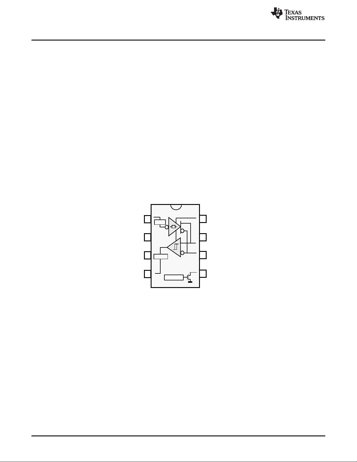
1 SN65HVD257 Basic Block Diagram and Pin Out....................................................................... 2
2 Typical SN65HVD257 Node To Build A Redundant Physical Layer Topology ..................................... 3
3 Typical Redundant Physical Layer Topology Using SN65HVD257 .................................................. 3
4 SN65HVD257 CAN EVM Top............................................................................................. 4
5 CAN EVM Schematic....................................................................................................... 5
6 Loopback Node 1 (JMP5 to JMP12) .................................................................................... 13
7 Loopback Node 2 (JMP10 to JMP13) .................................................................................. 13
List of Tables
1 SN65HVD257 CAN EVM Connections .................................................................................. 6
2 Main Supply and IO Header (JMP1) Connections ..................................................................... 7
3 CAN Bus Termination Configuration ..................................................................................... 9
4 CAN Bus Protection and Filtering Configuration ...................................................................... 10
5 EVM Digital IO Configuration ............................................................................................ 11
6 EVM Digital IO Configuration ............................................................................................ 11
SLLU172–August 2012 SN65HVD257 CAN EVM: Functional Safety and Redundant CAN Network
Submit Documentation Feedback
Copyright © 2012, Texas Instruments Incorporated
1
Page 2
S
CANH
CANL
FAULT
TXD
GND
V
CC
RXD
FAULT
DTO
DTO
Introduction
1 Introduction
1.1 Overview
Texas Instruments offers a broad portfolio of High Speed (HS) CAN transceivers compatible with the
ISO11898-2 and ISO11898-5 High Speed CAN standards. These include 5V VCConly, 3.3V VCConly, 5V
VCCwith IO level shifting and galvanic isolated CAN transceivers. These CAN transceiver families include
product mixes with varying features such as low power standby modes with and without wake up, silent
modes, loop back and diagnostic modes.
The Texas Instruments SN65HVD257 CAN EVM helps designers evaluate the operation and performance
of the SN65HVD257 CAN transceiver. The SN65HVD257 includes many features for functional safety
network implementation such as redundant CAN networks. The SN65HVD257 CAN EVM also provides
PCB footprints for different bus terminations, bus filtering, and protection concepts. The EVM is provided
with two SN65HVD257 devices installed. A separate EVM is available for the other CAN transceivers,
SN65HVD255 CAN EVM, and another EVM uses the galvanic isolated CAN transceiver family (ISO1050).
The SN65HVD257 meets the ISO1189-2 High Speed CAN (Controller Area Network) Physical Layer
standard (transceiver). It is designed as a next-generation CAN for the SN65HVD251 and ISO1050, but
with added features for functional safety networks such as redundant networks. It has very fast loop times
with a wide range of bus loading, allowing for data rates up to 1 megabit per second (Mbps) in long and
highly loaded networks and higher data rates in small networks. The device includes many protection
features to provide device and CAN network robustness. The device has two modes: normal mode and
silent mode, selected on pin 8. The FAULT pin indicates TXD dominant time out, RXD dominant time out,
thermal shut down and under voltage faults.
www.ti.com
Figure 1. SN65HVD257 Basic Block Diagram and Pin Out
1.2 Example Using the SN65HVD257 in a Redundant Physical Layer CAN Network Topology
CAN is designed for standard linear bus topology using 120Ω twisted pair cabling. The SN65HVD257
CAN device includes several features that allow use of the CAN physical layer in nonstandard topologies
with only one CAN link layer controller (μP) interface. The SN65HVD257 allows much greater flexibility in
the physical topology of the bus while reducing the digital controller and software costs. The combination
of RXD dominant time out and the FAULT output provides great flexibility, control and monitoring of these
applications.
A simple example of this flexibility is to use two SN65HVD257 devices combined logically in parallel via an
AND gate to build a redundant (parallel) physical layer (cabling and transceivers) CAN network. Adding a
2
logic XOR with a filter adds automatic detection for a fault where one of the 2 networks goes open
(recessive) in addition to the faults detected by the SN65HVD257.
To allow CAN’s bit-wise arbitration to work, the RXD outputs of the transceivers must be connected via
AND gate logic so that the link layer logic (μP) receives a dominant bit (low) from any of the branches; the
transceivers appear to the link layer and above as a single physical network. The RXD dominant time out
(DTO) feature prevents a bus stuck dominant fault in a single branch from taking down the entire network
by returning the RXD pin for the transceivers on the branch with the fault to the recessive state (high) after
SN65HVD257 CAN EVM: Functional Safety and Redundant CAN Network SLLU172–August 2012
Copyright © 2012, Texas Instruments Incorporated
Submit Documentation Feedback
Page 3

Bus 1 Bus 2
µP
SN65HVD257
RXD2
TDX
FLT2
SN65HVD257
FLT1
S1
S2
FLT3
RXD1
RXD
1A 2A
µP
SN65HVD257
RXD2
TDX
FLT2
SN65HVD257
FLT1
S1
S2
FLT3
RXD1
RXD
1n 2n
µP
SN65HVD257
RXD2
TDX
FLT2
SN65HVD257
FLT1
S1
S2
FLT3
RXD1
RXD
1n 2n
µP
SN65HVD257
RXD2
TDX
FLT2
SN65HVD257
FLT1
S1
S2
FLT3
RXD1
RXD
1Z 2Z
µP
SN65HVD257
RXD2
TDX
FLT2
SN65HVD257
FLT1
S1
S2
FLT3
Bus 1 Bus 2
RXD1
RXD
www.ti.com
Introduction
the t
RXD_DTO
time. The remaining branch of the network continues to function. The FAULT pin of the
transceivers on the branch with the fault shows this via the FAULT output to their host processors, which
will diagnose the failure condition. The S-pin (silent mode pin) may be used to put a branch in silent mode
to check each branch for other faults, including to look for bus open (recessive) faults. For automatic
detection of a branch being open (recessive), an XOR gate may be used to combine the RXD outputs of
both branches. During dominant bits (low), were the branches do not match the XOR, the circuit outputs a
logic high. A small RC filter on the output eliminates false outputs due to small timing differences in the
branches and transceivers. This XOR and the FAULT outputs of the transceivers could be connected to
edge triggered interrupt pins on the host microprocessor to enter specialize software routines if there is an
issue on the redundant network.
Thus it is possible build up a robust and redundant CAN network topology in a very simple and low cost
manner. These concepts can be expanded into other more complicated and flexible CAN network
topologies to solve various other system-level challenges with a networked infrastructure.
SLLU172–August 2012 SN65HVD257 CAN EVM: Functional Safety and Redundant CAN Network
Submit Documentation Feedback
Figure 2. Typical SN65HVD257 Node To Build A Redundant Physical Layer Topology
Figure 3. Typical Redundant Physical Layer Topology Using SN65HVD257
Copyright © 2012, Texas Instruments Incorporated
3
Page 4
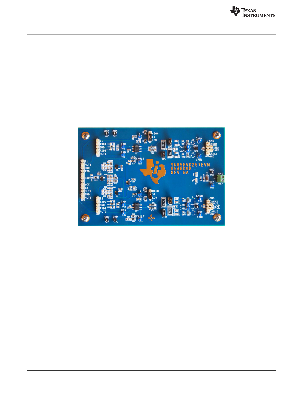
SN65HVD257 CAN EVM
2 SN65HVD257 CAN EVM
The EVM consists of 2 CAN bus “nodes” and the necessary logic to build functional safety networks. It is
pre-configured for redundant CAN network applications with the 2 CAN bus “nodes”, including the AND
gate to combine the RXD output from both buses and the XOR gate and filter (50kHz) to detect a bus
open fault. The EVM has simple connections to all necessary pins of the CAN transceiver devices and the
necessary logic to create a redundant network. Jumpers are provided where necessary to provide
flexibility for device pin and CAN bus configuration. There are test points (loops) for all main points where
probing is necessary for evaluation such as GND, VCC, TXD, RXD, CANH, CANL, S, FAULT. The EVM
supports many options for CAN bus configuration. It is pre-configured with two 120Ω resistors that may be
connected on the bus via jumpers; a single resistor is used with the EVM as a terminated line end (CAN is
defined for 120Ω impedance twisted pair cable) or both resistors in parallel for electrical measurements
representing the 60Ω load the transceiver “sees” in a properly terminated network (120Ω termination
resistors at both ends of the cable). If the application requires “split” termination, TVS diodes for protection
or Common Mode (CM) Choke the EVM has footprints available for these components via customer
installation of the desired component(s).
www.ti.com
Figure 4. SN65HVD257 CAN EVM Top
4
SN65HVD257 CAN EVM: Functional Safety and Redundant CAN Network SLLU172–August 2012
Copyright © 2012, Texas Instruments Incorporated
Submit Documentation Feedback
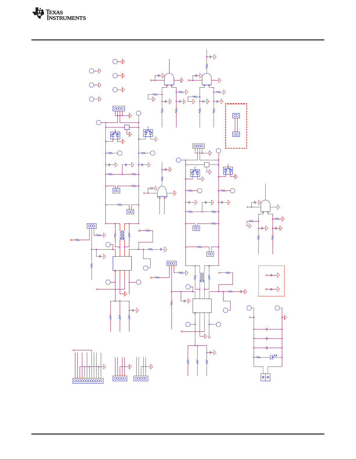
Page 5
Place near DUT Pin
LOOPBACK
S1
RXD1
FLT1
S1
RXDprime
TXDA
TXD1
TXDprime
TXDA
RXD1
RXD2
TXDprime
RXD2
TXDB
TXDprime
RXD1
FLT1
TXDprime
RXDprime
S2
FLT2
S1
TXD1
RXD1
FLT1
S2
TXD2
FLT2
RXD2
RXD2
FLT2
S2
TXD2
TXDprime
TXDB
FAULT3
RXD2
RXD1
FAULT3
VCC
VCC
VCC
VCC
VCC
VCC
VCC
VCC
VCC
VCC
VCC
VCC
VCC
VCC
RXD2
R28
DNI
C16
DNI
R44
10k
1
JMP2
HIGH
S1
LOW
C23
DNI
C21
DNI
D5
DNI
1
2
3
C19
DNI
C5
DNI
R11
0
TP4
CANH
1
R39
0
A
B
Y
VCC
GND
G08
U3
1
2
3 5
4
R40
4.7k
R14
330
TP20
CANH
1
C14
.1uF
R33
120
R1
4.7k
R24
DNI
C3
DNI
R27
0
C4
DNI
A
B
Y
VCC
GND
G86
U6
1
2
5
4
3
1
JMP1
S1
FLT1
GND
TXD
GND
RXD
GND
VCC
S2
FLT2
GND
FLT3
1
JMP10
GND
CANH2
CANL2
GND
R16
4.7k
R3
0
C29
0.1uF
C25
DNI
D1
DNI
1
2
3
C10
DNI
TP16
GND
1
R7 0
C2
DNI
R29
DNI
R35
0
R2
0
TP21
RXD
1
C24
DNI
R21
0
TP11
CANL
1
1
JMP7
S2
TXD2
GND
RXD2
FLT2
C26
DNI
L1
1
4
2
3
R8
0
A
B
Y
VCC
GND
G08
U4
1
2
3 5
4
1
JMP8
HIGH
S2
LOW
TP22
CANL
1
TP17
CANH
1
TP15
GND
1
TP8
RXD
1
TP1
GND
1
C17
DNI
U1
SN65HVD257
TXD1GND2Vcc3RXD
4
FLT
5
CANL
6
CANH
7
S
8
C13
1uF
R10
DNI
R17
0
U5
SN65HVD257
TXD1GND2Vcc3RXD
4
FLT
5
CANL
6
CANH
7
S
8
R19
330
C1
DNI
TP7
CANH
1
1
JMP5
GND
CANH1
CANL1
GND
1
JMP6
R6
330
R30
330
C9
0.1uF
R38
330
TP6
S
1
R12
120
1
JMP11
R45
10k
R47
3.3k
D3
GREEN
21
TP14
GND.
1
TP23
FAULT
1
R46
10k
R20
0
TP12
VCC
1
C28
1nF
TP9
CANL
1
C7
4.7uF
TP10
FAULT
1
1
JMP3
S1
TXD1
GND
RXD1
FLT1
C15
DNI
C20
DNI
TB1
1
2
R22
DNI
1
JMP4
R43
10k
C6
DNI
R26
0
TP2
GND
1
C27
4.7uF
A
B
Y
VCC
GND
G08
U2
1
2
3 5
4
R15
0
R9
120
TP19
S
1
1
JMP9
C12
10uF
R5
DNI
TP24
CANL
1
1
JMP13
R18
DNI
R32
0
R4
DNI
1
JMP12
R41
10k
C11
DNI
D7
1
1
3
3
2
2
R31 0
TP13
GND
1
D2
DNI
1
2
3
R13
DNI
L2
1
4
2
3
TP18
TXD
1
C22
DNI
R36
120
R42
10k
D4
DNI
1
2
3
TP5
TXD
1
TP3
GND
1
C8
0.1uF
R23
DNI
D6
1
1
3
3
2
2
R37
DNI
C18
0.1uF
R25
4.7k
R34
DNI
www.ti.com
SLLU172–August 2012 SN65HVD257 CAN EVM: Functional Safety and Redundant CAN Network
Submit Documentation Feedback
Figure 5. CAN EVM Schematic
Copyright © 2012, Texas Instruments Incorporated
SN65HVD257 CAN EVM
5
Page 6

SN65HVD257 CAN EVM
Connection Type Description
JMP1 12 pin header
JMP2 3 pin jumper S Mode Pin Control for transceiver 1
JMP3 5 pin header
JMP4 2 pin jumper
JMP5 4 pin header Connection for access to transceiver 1 CAN bus output: CANH1, CANL1, GND, GND
JMP6 2 pin jumper CAN termination to represent the combined 60Ω load for CAN transceiver parametric
JMP7 5 pin header
JMP8 3 pin jumper S Mode Pin Control for transceiver 2
JMP9 2 pin jumper
JMP10 4 pin header Connection for access to transceiver 2 CAN bus output: CANH2, CANL2, GND, GND.
JMP11 2 pin jumper CAN termination to represent the combined 60Ω load for CAN transceiver parametric
JMP12 2 pin jumper Next to JMP5 to allow jumping CAN bus 1 to CAN bus 2
JMP13 2 pin jumper Next to JMP10 to allow jumping CAN bus 1 to CAN bus 2
TB1 VCCsupply and GND connection for the EVM
TP1 Test Point GND test point
TP2 Test Point GND test point
TP3 Test Point GND test point
TP4 Test Point CANH (bus 1) test point
TP5 Test Point TXD, transceiver 1, test point
TP6 Test Point S, transceiver 1, test point
TP7 Test Point CANH (bus 1) via 330Ω serial resistor test point
TP8 Test Point RXD, transceiver 1, test point
TP9 Test Point CANL (bus 1) test point
TP10 Test Point FAULT (transceiver 1) test point
TP7 Test Point CANL (bus 1) via 330Ω serial resistor test point
TP12 Test Point Vcc test point
TP13 Test Point GND test point
TP14 Test Point GND test point
TP15 Test Point GND test point
TP16 Test Point GND test point
TP17 Test Point CANH (bus 2) test point
TP18 Test Point TXD, transceiver 2, test point
TP19 Test Point S, transceiver 2, test point
TP20 Test Point CANH (bus 2) via 330Ω serial resistor test point
TP21 Test Point RXD, transceiver 2, test point
TP22 Test Point CANL (bus 2) test point
TP23 Test Point FAULT (transceiver 2) test point
TP24 Test Point CANL (bus 2) via 330Ω serial resistor test point
www.ti.com
Table 1. SN65HVD257 CAN EVM Connections
Connection for access to all critical digital IO, supply and GND for driving the the CAN
transceivers externally with test equipment or interfaced to a processor EVM
Connection for access to all critical digital IO of the single transceiver 1 (bus) when EVM is used
for 2 separate buses
Connect 120Ω CAN termination to the bus. Used separately for a single termination if EVM is at
end of the CAN bus and termination isn’t in the cable. Used in combination with JMP6 to get to
second CAN termination to represent the combined 60Ω load for CAN transceiver parametric
measurement.
Connect 120Ω CAN termination to the bus. Used in combination with JMP4 to get to second
measurement.
Connection for access to all critical digital IO of the single transceiver 2 (bus) when EVM is used
for 2 separate buses
Connect 120Ω CAN termination to the bus. Used separately for a single termination if EVM is at
end of the CAN bus and termination is not in the cable. Used in combination with JMP6 to get to
second CAN termination to represent the combined 60Ω load for CAN transceiver parametric
measurement.
Connect 120Ω CAN termination to the bus. Used in combination with JMP4 to get to second
measurement.
2 pin terminal
block
6
SN65HVD257 CAN EVM: Functional Safety and Redundant CAN Network SLLU172–August 2012
Copyright © 2012, Texas Instruments Incorporated
Submit Documentation Feedback
Page 7

www.ti.com
SN65HVD257 EVM Setup and Operation for Redundant (Parallel Networks)
3 SN65HVD257 EVM Setup and Operation for Redundant (Parallel Networks)
This section describes the setup and operation of the EVM for parameter performance evaluation.
3.1 Overview and Basic Operation Settings
3.1.1 VCCPower Supply (TB1 or TP12 or JMP1)
The basic setup of the EVM requires a single power supply to evaluate transceiver and network design
performance. Supply VCCon TB1, JMP1 header or via the VCCand GND test point loops. The supplie
powerd must meet the required specification of VCCfor the transceiver being tested. LED D3 indicates VCC.
3.1.2 Main Supply and IO Header (JMP1)
All key IO and supply GND functions are brought to this header. It may be used to interface test
equipment, or a short cable can be made to connect to an existing customer application board or MCU or
DSP EVM board.
Table 2. Main Supply and IO Header (JMP1) Connections
Pin Connection Description
1 S1 Pin 5 of Transceiver 1. Used for Mode control.
2 FLT1 Pin 8 of Transceiver 1. Indicates fault with transceiver 1.
3 GND GND
4 TXD Pin 1 of Transceiver 1 and 2 (signal TXDprime). TXD (Transmit Data)
5 GND GND
6 RXD Pin 4 of Transceiver 1 and 2 combined via AND gate U2 (signal RXDprime). RXD (Receive Data)
7 GND GND
8 VCC Pin 3 of Transceiver. V
9 S2 Pin 5 of Transceiver 2. Used for Mode control.
10 FLT2 Pin 8 of Transceiver 2. Indicates fault with transceiver 2.
11 GND GND
12 FLT3 FAULT3: Open fault indicator. RXD (Pin 4) outputs of transceiver 1 and 2 combined via XOR gate U6 with
filter (signal FAULT3). Indicates bus open faults.
CC
3.1.3 TXD Input (JMP1)
The TXD input on JMP1 is connected via signal TXDprime to the TXD pin (pin 1) of both transceivers for
redundant (parallel) transmission on both buses. Individually this signal may be observed at the
transceiver pin via TP5 (transceiver 1) and TP18 (transceiver 2). The signal path TXDprime to the JMP1
header is pre-installed with a 0Ω series resistor, R10 and R34.
3.1.4 TXD Output (JMP1)
The RXD (combined) output of the transceivers via the AND gate for redundant (parallel) buses is JMP1.
Individually the RXD signals may be seen at the transceiver pin via TP8 (transceiver 1) and TP21
(transceiver 2). The combined RXD (RXDprime) signal path to the JMP1 header is pre-installed with a 0Ω
series resistor, R20 from the output of the AND gate U2.
3.1.5 S Pin (Mode Selection, pin 8) (JMP1, JMP2, JMP8, TP6 and TP19)
Pin 8 of the transceiver is the mode control pin of the device. Pin 8 of the devices is routed to JMP1,
JMP2 and JMP8.
SLLU172–August 2012 SN65HVD257 CAN EVM: Functional Safety and Redundant CAN Network
Submit Documentation Feedback
Copyright © 2012, Texas Instruments Incorporated
7
Page 8

SN65HVD257 EVM Setup and Operation for Redundant (Parallel Networks)
MODE SELECTION OPTIONS
JMP1 configuration:
Using header JMP1 (which assumes all the digital IO signals), VCC, GND are routed to an external
system. Ensure that the MODE (JMP2 and JMP8) jumper settings are not conflicting with signals to
JMP1.
JMP2, transceiver 1 configuration (3 way jumper):
If using separate IO inputs, use JMP2 to configure the S pin (pin 8) of transceiver 1 to a pull up to
VCC(Silent Mode), or pull down to GND (Normal Mode).
JMP8, transceiver 2 configuration (3 way jumper):
If using separate IO inputs, use JMP8 to configure the S pin (pin 8) of transceiver 2 to a pull up to
VCC (Silent Mode) or pull down to GND (Normal Mode).
TP6, transceiver 1 configuration:
This test point connects directly to the S pin (pin 8) of transceiver 1. Ensure that JMP1 and JMP2
are not configured to conflict if TP3 is used as the input connection.
TP19, transceiver 2 configuration:
This test point connects directly to the S pin (pin 8) of transceiver 2. Ensure that JMP1 and JMP8
are not configured to conflict if TP19 is used as the input connection.
3.1.6 FLT 1 (FAULT, pin 5, transceiver 1) (JMP1, TP10)
Pin 5 of transceiver 1 is the fault output of the transceiver. This output is routed to JMP1 and TP10. This
output indicates a RXD DTO, TXD DTO, Thermal Shut Down or undervoltage fault with transceiver 1.
www.ti.com
3.1.7 FLT 2 (FAULT, pin 5, transceiver 2) (JMP1, TP23)
Pin 5 of transceiver 2 is the fault output of the transceiver. This output is routed to JMP1 and TP23. This
output indicates a RXD DTO, TXD DTO, Thermal Shut Down or undervoltage fault with transceiver 2.
3.1.8 FLT 3 (bus open fault) (JMP1)
FLT3 is the fault output of the filtered XOR combination of the two transceiver (bus) outputs. FLT3 will
transition any time the two buses do not match, and thus indicate that one of the buses is open. The
output filter of this logic is pre-installed with a cut off frequency of 50kHz to all for large deviations in timing
between 2 parallel buses. This filter could be tuned by the user to match the filtering requirements of the
target application with respect to bit timing and how much reaction time, or “missing” dominant bits the
application requires, the XOR filter output to then show a transition to the monitoring processor.
3.1.9 JMP3 configuration (not used for Redundant Networks):
Using header JMP3 requires EVM reconfiguration for other applications.
3.1.10 JMP7 configuration (not used for Redundant Networks):
Using header JMP7 requires EVM reconfiguration for other applications.
8
SN65HVD257 CAN EVM: Functional Safety and Redundant CAN Network SLLU172–August 2012
Copyright © 2012, Texas Instruments Incorporated
Submit Documentation Feedback
Page 9

www.ti.com
SN65HVD257 EVM Setup and Operation for Redundant (Parallel Networks)
3.2 Using CAN Bus Load and Termination Configuration
Each bus of the EVM is populated with two 120Ω power resistors selectable via jumpers between CANH
and CANL. By using one of the resistors, the EVM may be used as a terminated end of a bus. For
electrical measurements to represent the total loading of the bus, use both 120Ω resistors in parallel to
give the standard 60Ω load for parametric measurement. The EVM also has footprints for customer
installation of split termination if the application requires it. The table below summarizes how to use these
termination options. If split termination is used, care must be taken to match the resistors. The commonmode filter frequency may be calculated by: fc= 1 / (2 π R C). Normally, the split capacitance is in the
range of 4.7nF to 100nF. Keep in mind that this is the common-mode filter frequency, not a differential
filter that will impact the differential CAN signal directly.
Table 3. CAN Bus Termination Configuration
"Termination Configuration Bus 1"
Standard Termination (120Ω) shorted open NA NA NA
60Ω load - Electrical Parameterics shorted shorted NA NA NA
Split Termination (Common Mode
Stabilization)
120Ω Resistors
JMP4 JMP6 R5 R13 C3
open open 60Ω 60Ω populated
Split Termination CM Stabilizing
Footprints Capacitor
"Termination Configuration Bus 2" 120Ω Resistors
JMP9 JMP11 R29 R37 C23
Standard Termination (120Ω) shorted open NA NA NA
60Ω load - Electrical Parameterics shorted shorted NA NA NA
Split Termination (Common Mode
Stabilization)
open open 60Ω 60Ω populated
Split Termination CM Stabilizing
Footprints Capacitor
SLLU172–August 2012 SN65HVD257 CAN EVM: Functional Safety and Redundant CAN Network
Submit Documentation Feedback
Copyright © 2012, Texas Instruments Incorporated
9
Page 10

SN65HVD257 EVM Setup and Operation for Redundant (Parallel Networks)
3.3 Using CAN Bus Protection and Filtering Configuration
The EVM also has component footprints for various protection schemes to enhance robustness for
extreme system-level EMC requirements. Table 4 summarizes these options. Typical examples of for
these components are: CM choke (TDK ACT45B series and EPCOS B82789 series from 11µH to 100µH),
bus filter capacitors are typically 100pF or less, TVS diodes from the MMBZ series 27V or lower, varistors
such as the TDK AVR series).
Table 4. CAN Bus Protection and Filtering Configuration
Protection and Filtering Footprint
Bus 1 Reference
Direct CAN transceiver to bus R7 and R11 populated with 0Ω (default
connection population)
Series Resistors or R7 and R11 or L1 Series resistance protection CAN R7 and R11 populated with MELF resistor
Common Mode Choke (common footprint) transceiver to bus connection as necessary for harsh EMC environment
CM choke (bus filter)
Bus Filtering Caps C2 and C5 Bus filter environment. Filter caps may be used in
Transient Protection Transient & ESD Protection population option footprints D1 and D2 for
D1 and D2,
C2 and C7 or D7
Use Case Population and Description
www.ti.com
L1 populated with CM choke to filter noise
as necessary for harsh EMC environment
Filter noise as necessary for harsh EMC
combination with L1 CM choke.
To add extra protection for system level
transients and ESD protection, use the
TVS diodes, or C2 and C7 or D7 for
varistors.
Protection and Filtering Footprint
Bus 2 Reference
Direct CAN transceiver to bus R31 and R35 populated with 0Ω (default
connection population)
Series Resistors or R31 and R35 or L2 Series resistance protection CAN R31 and R35 populated with MELF resistor
Common Mode Choke (common footprint) transceiver to bus connection as necessary for harsh EMC environment
CM choke (bus filter)
Bus Filtering Caps C22 and C25 Bus filter environment. Filter caps may be used in
Transient Protection Transient & ESD Protection population option footprints D4 and D5 for
D4 and D5,
C22 and C25 or D6
Use Case Population and Description
L2 populated with CM choke to filter noise
as necessary for harsh EMC environment
Filter noise as necessary for harsh EMC
combination with L2 CM choke.
To add extra protection for system level
transients and ESD protection, use the
TVS diodes or C22 and C25 or D6 for
varistors.
10
SN65HVD257 CAN EVM: Functional Safety and Redundant CAN Network SLLU172–August 2012
Copyright © 2012, Texas Instruments Incorporated
Submit Documentation Feedback
Page 11

www.ti.com
SN65HVD257 EVM Setup and Operation for Redundant (Parallel Networks)
3.4 Using Customer Installable IO Options for Current Limiting, Pull up or down, Noise Filtering
The EVM has footprints on the PCB for the installation of various filtering and protection options to adapt
the EVM to match CAN network topology requirements if the EVM is being used as a CAN node.
Each digital input or output pin has footprints to allow for series current limiting resistors (default populated
with 0Ω), pull up or down resistors depending on pin use and a capacitor to GND which, configured with
the serial resistor, implements RC filters (for noisy environments). The table below lists these features for
each of the digital input and output pins of the EVM. Replace or populate the RC components as
necessary for the application. The RC output filter pads for may be reused as a resistor divider network to
level shift the outputs down to 3.3V levels. The SN65HVD257 already has 3.3V compatible inputs on TXD
and S pins.
Table 5. EVM Digital IO Configuration
Signal Jumper
Description Type Pull Up
TXD U1 Input NA NA R8 (R4/R10) NA NA TXD input from JMP1 to TXD U1
TXD U2 Input NA NA NA NA TXD input from JMP1 to TXD U2
RXD U1 Output NA NA R17 C10
RXD U2 Output NA NA R17 C16
RXDprime Output NA NA R20 NA C15
S U1 Input R1 (JMP2) R2 NA C1
S U2 Input R25 (JMP2) R26 NA C21
FLT3 Output NA NA R47 (3.3k) NA C28 (1nF)
Pull
Down
R3 S (Mode) pin input from JMP1 or PU or
(JMP2) PD to S U1
R27 S (Mode) pin input from JMP1 or PU or
(JMP2) PD to S U2
Series R C to GND Description
R32
(R28/R34)
Pull Up or
Down
R44 PD RXD U1 output to AND Gate for
(10k) combined RXD redundant output
R43 PD RXD U1 output to AND Gate for
(10k) combined RXD redundant output
RXDprime is the combined RXD output
from the parallel CAN buses via AND
gate U2 which is routed to JMP1 as
RXD
FAULT3 is the combined RXD output
from the parallel CAN buses via XOR
gate U6 with the RC filter populated
which is routed to JMP1 as FLT3.
3.5 Using customer installable IO options for 3.3V IO
The EVM may be configured to have a 3.3V level output through the repurposing of the RC output filter
pads. These RC pads may be reused as a resistor divider network to level shift the outputs down to 3.3V
levels. The SN65HVD257 already has 3.3V compatible inputs on the TXD and S pins. Table 6 shows
some examples. For use in applications, calculations must be made to ensure the resistor divider network
chosen adheres to the application requirement. Considerations should include: current biasing in the
resistor network (loading, power), ensuring that the VOHand VOLof the divider will meet the VIHand V
input threshold levels of the host processor, and that the output of the resistor divider will be below the
absolute maximum rating of the host processor at the absolute maximum rating of the transceiver (or the
worst case corner the application will provide).
Table 6. EVM Digital IO Configuration
Output R1 Pad and Value R2 Pad and Value Description
RXDprime R20 = 3.9 kΩ C15 = 6.8 kΩ C15 pad is repurposed as R2.
FLT1 R15 = 0 Ω C6 = 8.2 kΩ R1 is the pull up R16. C6 pad is repurposed as R2.
R16 = 4.7k Ω
FLT2 "R39 = 0 Ω C26 = 8.2 kΩ R1 is the pull up R 40. C26 pad is repurposed as R2.
R40 = 4.7kΩ
FLT3 R47 = 3.9 kΩ C28 = 1nF and 6.8 kΩ C28 pad is repurposed as R2 and filter C (stacked
components).
SLLU172–August 2012 SN65HVD257 CAN EVM: Functional Safety and Redundant CAN Network
Submit Documentation Feedback
Copyright © 2012, Texas Instruments Incorporated
IL
11
Page 12

SN65HVD257 EVM Configuration for Two Independent Networks
4 SN65HVD257 EVM Configuration for Two Independent Networks
This section describes how to reconfigure the EVM into two independent networks. With this configuration,
the EVM could be used to host two node physical layers. The sections of the EVM not specifically
described below such as termination, filtering and protection are used in the same or similar fashion as
when the EVM is configured for a redundant network.
4.1 Transceiver 1 Header (JMP3)
4.1.1 TXD1 Input (JMP3, TP5)
The TXD1 input on JMP3 connects to transceiver 1 (U1) and TP5. To reconfigure the EVM, R8 must be
removed to disconnect TXDprime from U1, and R4 must be installed with a 0Ω resistor or current limiting
serial resistor of choice for the application to route the TXD1 signal to U1.
4.1.2 RXD1 Output (JMP3, TP8)
The RXD1 output of transceiver 1 (U1) is routed to JMP3 and TP8. If no parasitic loading to the combining
AND gate U2 is desired, then R17 may be removed.
4.1.3 S1 Input (Mode Selection,) (JMP3, JMP2 and TP6)
Pin 8 of the transceiver is the mode control pin of the device. Pin 8 of transceiver 1 is routed to JMP3,
JMP2 and TP6.
www.ti.com
MODE SELECTION OPTIONS
JMP3, transceiver 1 header configuration:
Header JMP3 handles all the digital IO signals for transceiver 1. JMP3 may be used to route these
signals to an external host processor or test system. Make sure that the MODE (JMP2) jumper
settings are not conflicting with signals to JMP3.
JMP2, transceiver 1 configuration (3 way jumper):
If the header is not used, then JMP2 may be used to configure the S pin (pin 8) of transceiver 1 to
a pull up to VCC(Silent Mode) or pull down to GND (Normal Mode).
TP6, transceiver 1 configuration:
This test point connects directly to the S pin (pin 8) of transceiver 1. Ensure that JMP3 and JMP2
are not configured to conflict if TP3 is used as the input connection.
4.1.4 FLT1 Output (JMP3, TP10)
Pin 5 of transceiver 1 is the fault output of the transceiver. This output routes to JMP3 and TP10. This
output indicates a RXD DTO, TXD DTO, Thermal Shut Down or undervoltage fault with transceiver 1.
4.2 Transceiver 2 Header (JMP7)
4.2.1 TXD2 Input (JMP7, TP18)
The TXD2 input on JMP7 is connected to transceiver 2 (U5) and TP5. To reconfigure the EVM, R32 must
be removed to disconnect TXDprime from U5, and R28 must be installed with a 0Ω resistor or current
limiting serial resistor of choice for the application to route the TXD2 signal to U5.
4.2.2 RXD2 Output (JMP7, TP21)
The RXD2 output of transceiver 2 (U5) is routed to JMP7 and TP21. If no parasitic loading to the
combining AND gate U2 is desired, then R21 may be removed.
12
SN65HVD257 CAN EVM: Functional Safety and Redundant CAN Network SLLU172–August 2012
Copyright © 2012, Texas Instruments Incorporated
Submit Documentation Feedback
Page 13
www.ti.com
SN65HVD257 EVM Configuration for Two Independent Networks
4.2.3 S2 Input (Mode Selection,) (JMP7, JMP8 and TP19)
Pin 8 of the transceiver is the mode control pin of the device. Pin 8 of transceiver 2 is routed to JMP7,
JMP8 and TP19.
MODE SELECTION OPTIONS
JMP7, transceiver 2 header configuration:
Header JMP7 handles all the digital IO signals for transceiver 2. JMP7 may be used to route the
signals to an external host processor or test system. Ensure that the MODE (JMP8) jumper settings
are not conflicting with signals to JMP7.
JMP8, transceiver 2 configuration (3 way jumper):
If the header is not used, then JMP8 may be used to configure S pin (pin 8) of transceiver 2 to a
pull up to VCC(Silent Mode) or pull down to GND (Normal Mode)
TP19, transceiver 2 configuration:
This test point connects directly to the S pin (pin 8) of transceiver 2. Ensure JMP7 and JMP8 are
not configured to conflict if TP19 is used as the input connection.
4.2.4 FLT2 Output (JMP7, TP23)
Pin 5 of transceiver 2 is the fault output of the transceiver. This output routed to JMP7 and TP23. This
output indicates a RXD DTO, TXD DTO, Thermal Shut Down or undervoltage fault with transceiver 2.
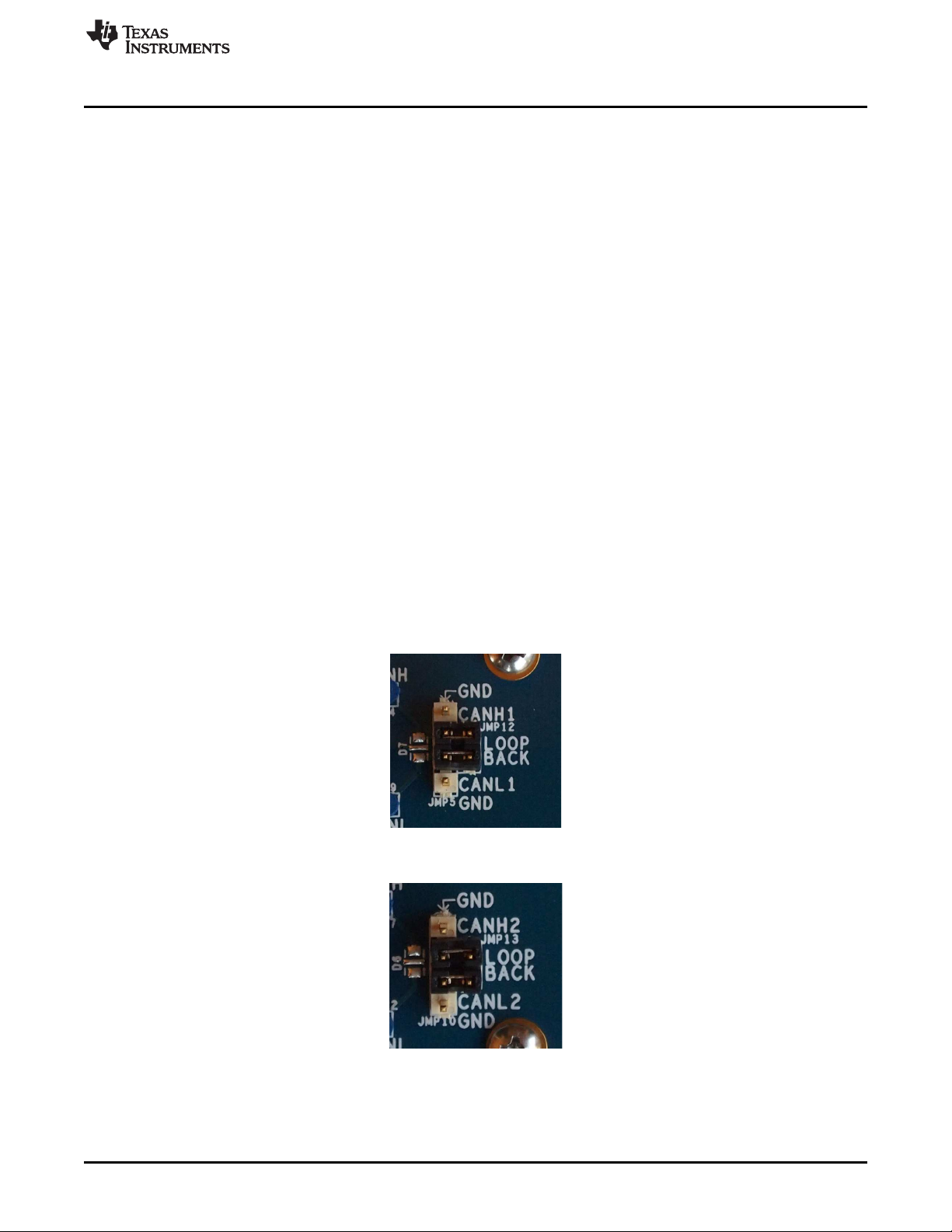
4.2.5 Loopback (single bus connection) of the Two Nodes (JMP12 and 13)
The EVM provides a path via JMP12 and JMP13 to connect to two nodes (transceivers) together on the
board as a single CAN network. On node 1 (transceiver 1, U1) connect CANH1 and CANL1 across JMP5
and JMP12 as shown below. On node 2 (transceiver 2, U5) connect CANH2 and CANL2 across JMP10
and JMP13 as shown below. CANH1 is now connected to CANH2 and CANL1 is connected to CANL2 in
one CAN network.
Figure 6. Loopback Node 1 (JMP5 to JMP12)
Figure 7. Loopback Node 2 (JMP10 to JMP13)
SLLU172–August 2012 SN65HVD257 CAN EVM: Functional Safety and Redundant CAN Network
Submit Documentation Feedback
Copyright © 2012, Texas Instruments Incorporated
13
Page 14

Bill of Material (BOM)
www.ti.com
5 Bill of Material (BOM)
Item QTY Reference Part Footprint Manufacturer
1 23 C16, C17, C18, C19, C20, 21, R22, R23, DNI 805 ANY
2 4 C2, C5, C22, C25 DNI 603 ANY
3 2 C7, C27 4.7uF 603 ANY
4 4 C8, C9, C18, C29 0.1uF 603 ANY
5 1 C12 10uF 1206 ANY
6 1 C13 1uF 603 ANY
7 1 C14 0.1uF 402 ANY
8 1 C28 1nF 805 ANY
9 4 D1, D2, D4, D5 DNI SOT_3DBZ ANY
10 1 D3 GREEN C170 ANY
11 2 D6, D7 DNI CA05M2S10T100HG TDK / EPCOS
12 1 JMP1 Header 1x12 HDR_THVT_1X12_100 ANY
13 2 JMP2, JMP8 Header 1x3 HDR_THVT_1X3_100 ANY
14 2 JMP3, JMP7 Header 1x5 HDR_THVT_1X5_100 ANY
15 6 Heder 1x2 HDR_THVT_1X2_100 ANY
16 2 JMP5, JMP10 Header 1x4 HDR_THVT_1X4_100 ANY
17 2 L1, L2 DNI TDK / EPCOS
18 4 R1, R16, R25, R40 4.7k 805 ANY
19 11 0 805 ANY
20 4 R3, R13, R29, R37 DNI 1210 ANY
21 5 R6, R14, 19, R30, R38 330 805 ANY
22 4 R7, R11, R31, R35 0 1206 ANY
23 4 R9, R12, R33, R36 120 2512 ANY
24 6 R41, R42, R43, R44, R45, R46 10k 805 ANY
25 1 R47 3.3k 805 ANY
26 1 TB1 2PIN_TERMINAL_BLOCK TB_THRTSCR_1x2_100 ANY
27 18 TP11, TP12, TP13, TP17, TP18, TP19, Test Point HDR_THVT_1x1_100 ANY
28 6 TP1, TP2, TP3, TP14, TP15, TP16 Test Point HDR_THVT_1x1_100 ANY
29 2 U1, U5 SN65HVD256D SOIC_8D TI
30 3 U2, U3, U4 SN74AHC1G86DBV SOT_5DBV TI
31 1 U6 SOT_5DBV TI
C1, C3, R4, C4, C6, R10, 10, C11, C15,
C23, R24, C24, C26, R28, R34
JMP4, JMP6, JMP9, JMP11, JMP12,
JMP13
ACT45B or B82789 series
CM choke
R2, R3, R8, R15, R17, R20, R21, R26,
R27, R32, R39
TP4, TP5, TP6, TP7, TP8,TP9, TP10,
TP20, TP21, TP22, TP23, TP24
14
SN65HVD257 CAN EVM: Functional Safety and Redundant CAN Network SLLU172–August 2012
Copyright © 2012, Texas Instruments Incorporated
Submit Documentation Feedback
Page 15

Evaluation Board/Kit Important Notice
Texas Instruments (TI) provides the enclosed product(s) under the following conditions:
This evaluation board/kit is intended for use for ENGINEERING DEVELOPMENT, DEMONSTRATION, OR EVALUATION PURPOSES
ONLY and is not considered by TI to be a finished end-product fit for general consumer use. Persons handling the product(s) must have
electronics training and observe good engineering practice standards. As such, the goods being provided are not intended to be complete
in terms of required design-, marketing-, and/or manufacturing-related protective considerations, including product safety and environmental
measures typically found in end products that incorporate such semiconductor components or circuit boards. This evaluation board/kit does
not fall within the scope of the European Union directives regarding electromagnetic compatibility, restricted substances (RoHS), recycling
(WEEE), FCC, CE or UL, and therefore may not meet the technical requirements of these directives or other related directives.
Should this evaluation board/kit not meet the specifications indicated in the User’s Guide, the board/kit may be returned within 30 days from
the date of delivery for a full refund. THE FOREGOING WARRANTY IS THE EXCLUSIVE WARRANTY MADE BY SELLER TO BUYER
AND IS IN LIEU OF ALL OTHER WARRANTIES, EXPRESSED, IMPLIED, OR STATUTORY, INCLUDING ANY WARRANTY OF
MERCHANTABILITY OR FITNESS FOR ANY PARTICULAR PURPOSE.
The user assumes all responsibility and liability for proper and safe handling of the goods. Further, the user indemnifies TI from all claims
arising from the handling or use of the goods. Due to the open construction of the product, it is the user’s responsibility to take any and all
appropriate precautions with regard to electrostatic discharge.
EXCEPT TO THE EXTENT OF THE INDEMNITY SET FORTH ABOVE, NEITHER PARTY SHALL BE LIABLE TO THE OTHER FOR ANY
INDIRECT, SPECIAL, INCIDENTAL, OR CONSEQUENTIAL DAMAGES.
TI currently deals with a variety of customers for products, and therefore our arrangement with the user is not exclusive.
TI assumes no liability for applications assistance, customer product design, software performance, or infringement of patents or
services described herein.
Please read the User’s Guide and, specifically, the Warnings and Restrictions notice in the User’s Guide prior to handling the product. This
notice contains important safety information about temperatures and voltages. For additional information on TI’s environmental and/or
safety programs, please contact the TI application engineer or visit www.ti.com/esh.
No license is granted under any patent right or other intellectual property right of TI covering or relating to any machine, process, or
combination in which such TI products or services might be or are used.
FCC Warning
This evaluation board/kit is intended for use for ENGINEERING DEVELOPMENT, DEMONSTRATION, OR EVALUATION PURPOSES
ONLY and is not considered by TI to be a finished end-product fit for general consumer use. It generates, uses, and can radiate radio
frequency energy and has not been tested for compliance with the limits of computing devices pursuant to part 15 of FCC rules, which are
designed to provide reasonable protection against radio frequency interference. Operation of this equipment in other environments may
cause interference with radio communications, in which case the user at his own expense will be required to take whatever measures may
be required to correct this interference.
EVM Warnings and Restrictions
It is important to operate this EVM within the input voltage range of and the output voltage range of .
Exceeding the specified input range may cause unexpected operation and/or irreversible damage to the EVM. If there are questions
concerning the input range, please contact a TI field representative prior to connecting the input power.
Applying loads outside of the specified output range may result in unintended operation and/or possible permanent damage to the EVM.
Please consult the EVM User's Guide prior to connecting any load to the EVM output. If there is uncertainty as to the load specification,
please contact a TI field representative.
During normal operation, some circuit components may have case temperatures greater than . The EVM is designed to operate properly
with certain components above as long as the input and output ranges are maintained. These components include but are not limited to
linear regulators, switching transistors, pass transistors, and current sense resistors. These types of devices can be identified using the
EVM schematic located in the EVM User's Guide. When placing measurement probes near these devices during operation, please be
aware that these devices may be very warm to the touch.
Mailing Address: Texas Instruments, Post Office Box 655303, Dallas, Texas 75265
Copyright © 2012, Texas Instruments Incorporated
Page 16

IMPORTANT NOTICE
Texas Instruments Incorporated and its subsidiaries (TI) reserve the right to make corrections, enhancements, improvements and other
changes to its semiconductor products and services per JESD46, latest issue, and to discontinue any product or service per JESD48, latest
issue. Buyers should obtain the latest relevant information before placing orders and should verify that such information is current and
complete. All semiconductor products (also referred to herein as “components”) are sold subject to TI’s terms and conditions of sale
supplied at the time of order acknowledgment.
TI warrants performance of its components to the specifications applicable at the time of sale, in accordance with the warranty in TI’s terms
and conditions of sale of semiconductor products. Testing and other quality control techniques are used to the extent TI deems necessary
to support this warranty. Except where mandated by applicable law, testing of all parameters of each component is not necessarily
performed.
TI assumes no liability for applications assistance or the design of Buyers’ products. Buyers are responsible for their products and
applications using TI components. To minimize the risks associated with Buyers’ products and applications, Buyers should provide
adequate design and operating safeguards.
TI does not warrant or represent that any license, either express or implied, is granted under any patent right, copyright, mask work right, or
other intellectual property right relating to any combination, machine, or process in which TI components or services are used. Information
published by TI regarding third-party products or services does not constitute a license to use such products or services or a warranty or
endorsement thereof. Use of such information may require a license from a third party under the patents or other intellectual property of the
third party, or a license from TI under the patents or other intellectual property of TI.
Reproduction of significant portions of TI information in TI data books or data sheets is permissible only if reproduction is without alteration
and is accompanied by all associated warranties, conditions, limitations, and notices. TI is not responsible or liable for such altered
documentation. Information of third parties may be subject to additional restrictions.
Resale of TI components or services with statements different from or beyond the parameters stated by TI for that component or service
voids all express and any implied warranties for the associated TI component or service and is an unfair and deceptive business practice.
TI is not responsible or liable for any such statements.
Buyer acknowledges and agrees that it is solely responsible for compliance with all legal, regulatory and safety-related requirements
concerning its products, and any use of TI components in its applications, notwithstanding any applications-related information or support
that may be provided by TI. Buyer represents and agrees that it has all the necessary expertise to create and implement safeguards which
anticipate dangerous consequences of failures, monitor failures and their consequences, lessen the likelihood of failures that might cause
harm and take appropriate remedial actions. Buyer will fully indemnify TI and its representatives against any damages arising out of the use
of any TI components in safety-critical applications.
In some cases, TI components may be promoted specifically to facilitate safety-related applications. With such components, TI’s goal is to
help enable customers to design and create their own end-product solutions that meet applicable functional safety standards and
requirements. Nonetheless, such components are subject to these terms.
No TI components are authorized for use in FDA Class III (or similar life-critical medical equipment) unless authorized officers of the parties
have executed a special agreement specifically governing such use.
Only those TI components which TI has specifically designated as military grade or “enhanced plastic” are designed and intended for use in
military/aerospace applications or environments. Buyer acknowledges and agrees that any military or aerospace use of TI components
which have not been so designated is solely at the Buyer's risk, and that Buyer is solely responsible for compliance with all legal and
regulatory requirements in connection with such use.
TI has specifically designated certain components which meet ISO/TS16949 requirements, mainly for automotive use. Components which
have not been so designated are neither designed nor intended for automotive use; and TI will not be responsible for any failure of such
components to meet such requirements.
Products Applications
Audio www.ti.com/audio Automotive and Transportation www.ti.com/automotive
Amplifiers amplifier.ti.com Communications and Telecom www.ti.com/communications
Data Converters dataconverter.ti.com Computers and Peripherals www.ti.com/computers
DLP® Products www.dlp.com Consumer Electronics www.ti.com/consumer-apps
DSP dsp.ti.com Energy and Lighting www.ti.com/energy
Clocks and Timers www.ti.com/clocks Industrial www.ti.com/industrial
Interface interface.ti.com Medical www.ti.com/medical
Logic logic.ti.com Security www.ti.com/security
Power Mgmt power.ti.com Space, Avionics and Defense www.ti.com/space-avionics-defense
Microcontrollers microcontroller.ti.com Video and Imaging www.ti.com/video
RFID www.ti-rfid.com
OMAP Applications Processors www.ti.com/omap TI E2E Community e2e.ti.com
Wireless Connectivity www.ti.com/wirelessconnectivity
Mailing Address: Texas Instruments, Post Office Box 655303, Dallas, Texas 75265
Copyright © 2012, Texas Instruments Incorporated
Page 17

Mouser Electronics
Authorized Distributor
Click to View Pricing, Inventory, Delivery & Lifecycle Information:
Texas Instruments:
SN65HVD257EVM
 Loading...