

Page 1

User’s Guide
2000 PCI Bus Solutions
SCPU005
Page 2

IMPORTANT NOTICE
T exas Instruments and its subsidiaries (TI) reserve the right to make changes to their products or to discontinue
any product or service without notice, and advise customers to obtain the latest version of relevant information
to verify, before placing orders, that information being relied on is current and complete. All products are sold
subject to the terms and conditions of sale supplied at the time of order acknowledgment, including those
pertaining to warranty, patent infringement, and limitation of liability.
TI warrants performance of its semiconductor products to the specifications applicable at the time of sale in
accordance with TI’s standard warranty. Testing and other quality control techniques are utilized to the extent
TI deems necessary to support this warranty . Specific testing of all parameters of each device is not necessarily
performed, except those mandated by government requirements.
Customers are responsible for their applications using TI components.
In order to minimize risks associated with the customer’s applications, adequate design and operating
safeguards must be provided by the customer to minimize inherent or procedural hazards.
TI assumes no liability for applications assistance or customer product design. TI does not warrant or represent
that any license, either express or implied, is granted under any patent right, copyright, mask work right, or other
intellectual property right of TI covering or relating to any combination, machine, or process in which such
semiconductor products or services might be or are used. TI’s publication of information regarding any third
party’s products or services does not constitute TI’s approval, warranty or endorsement thereof.
Copyright 2000, Texas Instruments Incorporated
Page 3

About This Manual
This manual is designed to assist the user of the PCI2250 evaluation module
(EVM). It provides descriptions of parts, features, and operating requirements
of the EVM that are necessary or useful to obtain maximum benefit from EVM
use.
How to Use This Manual
This document contains the following chapters:
Information About Cautions and Warnings
Preface
Read This First
Chapter 1,
materials for the EVM kit.
Chapter 2,
requirements for any PC system on which the PCI2250 EVM is to be run.
Chapter 3,
routing as related to the edge connectors on the board.
Chapter 4,
components such as pins, jumpers, connectors, and LEDs.
Introduction
Software Requirements
Configuration
Board Configuration
, provides a brief description of the EVM, and a bill of
Information About Cautions and Warnings
This book may contain cautions and warnings.
This is an example of a caution statement.
A caution statement describes a situation that could potentially
damage your software or equipment.
This is an example of a warning statement.
, details the minimum software
, explains secondary bus masters and interrupt
, describes the location and purpose of board
A warning statement describes a situation that could potentially
cause harm to you
.
Read This First
iii
Page 4

Trademarks
The information in a caution or a warning is provided for your protection.
Please read each caution and warning carefully.
Related Documentation From Texas Instruments
PCI2250 PCI-to-PCI Bridge Data Manual
PCI2250 Implementation Guide
, SCPU008
, TI Literature Number – SCPS051
Connecting ENUM Terminal to an External Open-Drain Buffer
Number – SCPA027
FCC Warning
This equipment is intended for use in a laboratory test environment only . It generates, uses, and can radiate radio frequency energy and has not been tested
for compliance with the limits of computing devices pursuant to subpart J of
part 15 of FCC rules, which are designed to provide reasonable protection
against radio frequency interference. Operation of this equipment in other environments may cause interference with radio communications, in which case
the user at his own expense will be required to take whatever measures may
be required to correct this interference.
Trademarks
Intel is a trademark of Intel Corporation.
Windows is a trademark of Microsoft Corporation. (Windows 95, Windows)
Windows NT is a trademark of Microsoft Corporation. (Windows NT )
, TI Literature
CompactPCI is a trademark of PICMG – PCI Industrial Computer Manufacturers Group, Inc.
Other trademarks are the property of their respective owners.
iv
Page 5

Running Title—Attribute Reference
Contents
1 Introduction 1-1. . . . . . . . . . . . . . . . . . . . . . . . . . . . . . . . . . . . . . . . . . . . . . . . . . . . . . . . . . . . . . . . . . . . .
1.1 Introduction 1-2. . . . . . . . . . . . . . . . . . . . . . . . . . . . . . . . . . . . . . . . . . . . . . . . . . . . . . . . . . . . . . . .
1.2 Evaluation Kit Bill of Materials 1-2. . . . . . . . . . . . . . . . . . . . . . . . . . . . . . . . . . . . . . . . . . . . . . . .
2 Software Requirements 2-1. . . . . . . . . . . . . . . . . . . . . . . . . . . . . . . . . . . . . . . . . . . . . . . . . . . . . . . . . .
2.1 Software Requirements 2-2. . . . . . . . . . . . . . . . . . . . . . . . . . . . . . . . . . . . . . . . . . . . . . . . . . . . .
3 Configuration 3-1. . . . . . . . . . . . . . . . . . . . . . . . . . . . . . . . . . . . . . . . . . . . . . . . . . . . . . . . . . . . . . . . . . .
3.1 Configuration 3-2. . . . . . . . . . . . . . . . . . . . . . . . . . . . . . . . . . . . . . . . . . . . . . . . . . . . . . . . . . . . . .
4 Board Configuration 4-1. . . . . . . . . . . . . . . . . . . . . . . . . . . . . . . . . . . . . . . . . . . . . . . . . . . . . . . . . . . . .
4.1 Board Jumpers 4-2. . . . . . . . . . . . . . . . . . . . . . . . . . . . . . . . . . . . . . . . . . . . . . . . . . . . . . . . . . . . .
4.2 PCI2250 Mode Select Pins 4-3. . . . . . . . . . . . . . . . . . . . . . . . . . . . . . . . . . . . . . . . . . . . . . . . . .
4.2.1 Clock Run Mode 4-3. . . . . . . . . . . . . . . . . . . . . . . . . . . . . . . . . . . . . . . . . . . . . . . . . . . .
4.2.2 CompactPCI Hot Swap 4-3. . . . . . . . . . . . . . . . . . . . . . . . . . . . . . . . . . . . . . . . . . . . .
4.2.3 Intel Mode 4-3. . . . . . . . . . . . . . . . . . . . . . . . . . . . . . . . . . . . . . . . . . . . . . . . . . . . . . . .
4.3 LED Indicators 4-4. . . . . . . . . . . . . . . . . . . . . . . . . . . . . . . . . . . . . . . . . . . . . . . . . . . . . . . . . . . . .
4.3.1 D1 ENUM 4-4. . . . . . . . . . . . . . . . . . . . . . . . . . . . . . . . . . . . . . . . . . . . . . . . . . . . . . . . . .
4.3.2 D2 HSLED 4-4. . . . . . . . . . . . . . . . . . . . . . . . . . . . . . . . . . . . . . . . . . . . . . . . . . . . . . . . .
4.3.3 D3 C1_PRES 4-4. . . . . . . . . . . . . . . . . . . . . . . . . . . . . . . . . . . . . . . . . . . . . . . . . . . . . . .
4.3.4 D4 C2_PRES 4-4. . . . . . . . . . . . . . . . . . . . . . . . . . . . . . . . . . . . . . . . . . . . . . . . . . . . . . .
4.3.5 D5 C3_PRES 4-4. . . . . . . . . . . . . . . . . . . . . . . . . . . . . . . . . . . . . . . . . . . . . . . . . . . . . . .
4.3.6 D6 EVM3V 4-4. . . . . . . . . . . . . . . . . . . . . . . . . . . . . . . . . . . . . . . . . . . . . . . . . . . . . . . . .
4.3.7 D7 PCU3V 4-4. . . . . . . . . . . . . . . . . . . . . . . . . . . . . . . . . . . . . . . . . . . . . . . . . . . . . . . . .
4.4 Power Measurements 4-4. . . . . . . . . . . . . . . . . . . . . . . . . . . . . . . . . . . . . . . . . . . . . . . . . . . . . . .
4.5 Mictor Connector Definition 4-5. . . . . . . . . . . . . . . . . . . . . . . . . . . . . . . . . . . . . . . . . . . . . . . . . .
4.6 Board Description 4-6. . . . . . . . . . . . . . . . . . . . . . . . . . . . . . . . . . . . . . . . . . . . . . . . . . . . . . . . . .
Chapter Title—Attribute Reference
v
Page 6

Running Title—Attribute Reference
Figures
4–1 Part and Jumper Locations 4-6. . . . . . . . . . . . . . . . . . . . . . . . . . . . . . . . . . . . . . . . . . . . . . . . . . . . .
4–2 Schematic Diagram 4-7. . . . . . . . . . . . . . . . . . . . . . . . . . . . . . . . . . . . . . . . . . . . . . . . . . . . . . . . . . .
T ables
3–1 Edge Connector Device ID 3-2. . . . . . . . . . . . . . . . . . . . . . . . . . . . . . . . . . . . . . . . . . . . . . . . . . . . .
3–2 Edge Connector Interrupt Routing 3-2. . . . . . . . . . . . . . . . . . . . . . . . . . . . . . . . . . . . . . . . . . . . . . .
4–1 Jumper Definitions 4-2. . . . . . . . . . . . . . . . . . . . . . . . . . . . . . . . . . . . . . . . . . . . . . . . . . . . . . . . . . . .
4–2 Mode Select Jumper Settings 4-3. . . . . . . . . . . . . . . . . . . . . . . . . . . . . . . . . . . . . . . . . . . . . . . . . . .
4–3 HP Logic Analyzer POD Definition 4-5. . . . . . . . . . . . . . . . . . . . . . . . . . . . . . . . . . . . . . . . . . . . . . .
4–4 PCI2250 EVM Bill of Materials 4-15. . . . . . . . . . . . . . . . . . . . . . . . . . . . . . . . . . . . . . . . . . . . . . . . .
vi
Page 7

Chapter 1
Introduction
This chapter provides a brief overview of the PCI2250 evaluation module,
along with a bill of materials for the EVM kit.
Topic Page
1.1 Introduction 1-2. . . . . . . . . . . . . . . . . . . . . . . . . . . . . . . . . . . . . . . . . . . . . . . . . .
1.2 Evaluation Kit Bill of Materials 1-2. . . . . . . . . . . . . . . . . . . . . . . . . . . . . . . . .
1-1
Page 8

Introduction
1.1 Introduction
This document is intended to assist the user of the PCI2250 evaluation module
(EVM), EVM2250B. Included within this document are instructions detailing
the proper setup and configuration necessary to operate the PCI2250 EVM.
1.2 Evaluation Kit Bill of Materials
The PCI2250 EVM consists of the following items:
Item Nomenclature Quantity
EVM2250B PCI to PCI adapter card assembly 1
3.5” Diskette PCIBus and PCIBus95 utility programs 1
1-2
Page 9

Chapter 2
Software Requirements
This chapter provides the minimum software requirements for any PC system
on which the PCI2250 EVM is to be used.
Topic Page
2.1 Software Requirements 2-2. . . . . . . . . . . . . . . . . . . . . . . . . . . . . . . . . . . . . . . .
Software Requirements
2-1
Page 10

Software Requirements
2.1 Software Requirements
The EVM2250B evaluation board will work in any system that meets the
following requirements:
BIOS which supports the
Operating system that supports the
PCI Bridge Specification 1.0
PCI Bridge Specification 1.0
.
.
In the majority of today’s computer systems, bridge support is built into the
BIOS. Many operation systems, like Windows 95/98 and Windows NT,
have support for bridges.
2-2
Page 11

Chapter 3
Configuration
This chapter explains secondary bus masters and interrupt routing as related
to edge connectors on the board.
Topic Page
3.1 Configuration 3-2. . . . . . . . . . . . . . . . . . . . . . . . . . . . . . . . . . . . . . . . . . . . . . . . .
Configuration
3-1
Page 12

Configuration
3.1 Configuration
The PCI2250 supports four secondary bus masters. Due to board space, only
three masters are supported with the EVM2250B board. The three supported
masters can be plugged into three edge connectors labeled P1, P2, and P3.
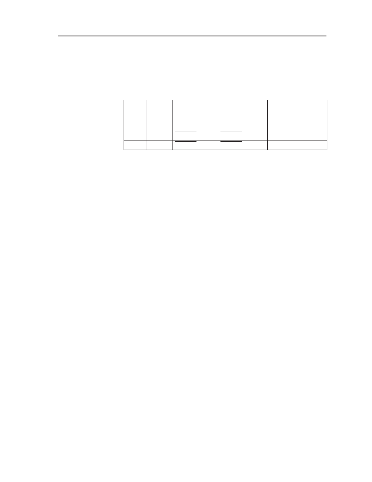
These edge connectors are configured based on the Table 3–1.
Table 3–1.Edge Connector Device ID
Edge Connector Resistor Installed Slot ID
P1 R20
R21 (default)
R22
P2 R23 (default)
R24
R25
P3 R26 (default)
R27
R28
The interrupts for each connector on the secondary bus are routed according
to the
PCI Local Bus Specification Revision 2.2
depicts how the interrupts are routed on the EVM2250B evaluation board.
Table 3–2.Edge Connector Interrupt Routing
Edge Connector Interrupt Routed on INTX on P1
P1 INTA
INTB
INTC
INTD
P2 INTA
INTB
INTC
INTD
0
4 (default)
8
1 (default)
5
9
2 (default)
6
A
, section 2.2.6. Table 3–2
INTA
INTB
INTC
INTD
INTB
INTC
INTD
INTA
3-2
P3 INTA
INTB
INTC
INTD
INTC
INTD
INTA
INTB
Page 13

Chapter 4
Board Configuration
This chapter describes the location and purpose of board components such
as pins, jumpers, connectors, and LEDs.
Topic Page
4.1 Board Jumpers 4-2. . . . . . . . . . . . . . . . . . . . . . . . . . . . . . . . . . . . . . . . . . . . . . .
4.2 PCI2250 Mode Select Pins 4-3. . . . . . . . . . . . . . . . . . . . . . . . . . . . . . . . . . . . .
4.3 LED Indicators 4-4. . . . . . . . . . . . . . . . . . . . . . . . . . . . . . . . . . . . . . . . . . . . . . . .
4.4 Power Measurements 4-4. . . . . . . . . . . . . . . . . . . . . . . . . . . . . . . . . . . . . . . . .
4.5 Mictor Connector Definition 4-5. . . . . . . . . . . . . . . . . . . . . . . . . . . . . . . . . . . .
4.6 Board Description 4-6. . . . . . . . . . . . . . . . . . . . . . . . . . . . . . . . . . . . . . . . . . . . .
Board Configuration
4-1
Page 14

Board Jumpers
4.1 Board Jumpers
Built into the evaluation board is the ability to monitor and test all the
capabilities of the PCI2250. There are many jumpers located on the evaluation
board (J1 through J12), which allow an engineer to perform tests ranging from
measuring power to changing the arbitration of the PCI2250. All of these
jumpers are defined in Table 4–1.
Table 4–1.Jumper Definitions
Jumper Description
J1 P_MFUNC select. This jumper is used to select whether to route
J5 & J6 Jumpers J5 and J6 are used to control the mode select inputs to the
J7 S_MFUNC select. This jumper is used to select whether to route
J8 Arbitration support. By cutting the trace across this jumper and installing
J9 S_VCCP for the PCI2250. This jumper can be used to measure the power
P_MFUNC to P_LOCK
PCI2250.
S_MFUNC to S_LOCK or S_CLKRUN/HS_SWITCH.
R10 an external arbiter can be used.
consumed through the S_VCCP.
or P_CLKRUN/HS_ENUM.
J10 P_VCCP for the PCI2250. This jumper can be used to measure the power
consumed through the P_VCCP.
J11 Core VCC for the PCI2250. This jumper can be used to measure the
power consumed by the PCI2250 core logic.
J12 S_VIO select. This jumper is used to select between 3.3-V and 5.0-V
signaling environments on the secondary bus.
4-2
Page 15
4.2 PCI2250 Mode Select Pins
The PCI2250 has three modes of operation based on the value of the mode
select pins MS0 (J6-2) and MS1 (J5-2). Table 4–2 shows the jumper settings
for the different modes of operation.
Table 4–2.Mode Select Jumper Settings
J6 J5 P_MFUNC S_MFUNC Mode
2–3 2–3 HS_ENUM HS_SWITCH TI hot-swap
2–3 1–2 P_CLKRUN S_CLKRUN TI clock run
1–2 2–3 P_LOCK S_LOCK Intel B2 support
1–2 1–2 P_LOCK S_LOCK Intel B3 support
4.2.1 Clock Run Mode
When the PCI2250 is in clock run mode, jumpers J1 and J7 should not be
jumpered. The clock run signals can be pulled directly from pin 2 of the jumper
headers.
PCI2250 Mode Select Pins
4.2.2 CompactPCI Hot Swap
When hot-swap mode is selected, jumpers J1 and J7 should have a jumper
between pins 2 and 3, routing the multifunction pins to the CompactPCI test
points.
4.2.3 Intel Mode
When Intel mode is selected, jumpers J1 and J7 should have a jumper
between pins 1 and 2, routing the multifunction pins to the LOCK
connectors.
pins on the
Board Configuration
4-3
Page 16

LED Indicators
4.3 LED Indicators
4.3.1 D1 ENUM
4.3.2 D2 HSLED
4.3.3 D3 C1_PRES
4.3.4 D4 C2_PRES
When the PCI2250 is configured in CompactPCI mode, this LED lights when
the ENUM signal is driven low.
When the PCI2250 is configured in Compact PCI mode, this LED lights when
the HSLED signal is driven low.
D3 lights when a PCI board that has the PRSNT2 pin tied to ground is inserted
in connector P1.
D4 lights when a PCI board that has the PRSNT2 pin tied to ground is inserted
in connector P2.
4.3.5 D5 C3_PRES
D5 lights when a PCI board that has the PRSNT2 pin tied to ground is inserted
in connector P3.
4.3.6 D6 EVM3V
D6 lights to indicate that 3.3 V is available on the secondary bus.
4.3.7 D7 PCU3V
D7 lights to indicate that the PCI2250 has power applied to the core logic.
4.4 Power Measurements
In order to measure the current drawn by the core logic or one of the VIO rails
of the PCI2250 it is necessary to isolate the power supplied to these pins from
the rest of the system. This can be done by cutting the trace that connects the
power pins to the system. Jumpers J6, J7, and J8 have default traces that are
provided for this purpose. After the traces are cut, an external power supply
can be used along with a current meter to measure the current used by the
selected power rail. The power rail can then be reconnected to the system by
placing a jumper across the cut trace.
4-4
Page 17

4.5 Mictor Connector Definition
Connectors MC1 and MC2 can be used to connect a logic analyzer to the
secondary PCI bus. See Table 4–3 for a listing of the signals for each logic
analyzer POD.
Table 4–3.HP Logic Analyzer POD Definition
Pin Number POD 1 POD 2 POD 3 POD 4
0 S_AD0 S_AD16 S_PAR S_REQ64
1 S_AD1 S_AD17 S_SERR S_ACK64
2 S_AD2 S_AD18 S_PERR C1_IDSEL
3 S_AD3 S_AD19 S_STOP C1_GNT
4 S_AD4 S_AD20 S_DEVSEL C1_REQ
5 S_AD5 S_AD21 S_C/BE0 C2_IDSEL
6 S_AD6 S_AD22 S_C/BE1 C2_GNT
7 S_AD7 S_AD23 S_C/BE2 S_FRAME
Mictor Connector Definition
8 S_AD8 S_AD24 S_C/BE3 S_IRDY
9 S_AD9 S_AD25 S_RST C2_REQ
10 S_AD10 S_AD26 INTA S_TRDY
11 S_AD11 S_AD27 INTB C3_IDSEL
12 S_AD12 S_AD28 INTC C3_GNT
13 S_AD13 S_AD29 INTD C3_REQ
14 S_AD14 S_AD30 NC NC
15 S_AD15 S_AD31 NC NC
Board Configuration
4-5
Page 18

Board Description
4.6 Board Description
The board layout is shown in Figure 4–1. The schematic diagram of the board
is in Figure 4–2. Table 4–4, bill of materials, is a list of the parts used to
assemble the board.
Figure 4–1.Part and Jumper Locations
151413
121110
S_AD11
S_AD13
S_AD12
S_AD15
S_AD14
POD1
P2B1
9
8
S_AD09
S_AD08
S_AD10
0
S_AD01
S_AD00
9
8
S_AD25
S_AD24
0
S_AD17
S_AD16
9
8
S_RST
C/BE3
0
S_SERR
S_PAR
9
8
C2_REQ
S_IRDY
0
S_ACK64
S_REQ64
S_AD03
S_AD02
S_AD27
S_AD26
S_AD19
S_AD18
INTB
INTA
S_STOP
S_PERR
C3_IDSEL
S_TRDY
C1_GNT
C1_IDSEL
S_AD06
S_AD05
S_AD04
121110
S_AD30
S_AD29
S_AD28
S_AD22
S_AD21
S_AD20
121110
INDC
S_C/BE
S_C/BE
S_DEVSEL
1
0
121110
C3_GNT
C2_GNT
C2_IDSEL
C1_REQ
CLK C1_PCLK
7654321
S_AD07
151413
POD2
S_AD31
7654321
S_AD23
151413
POD3
NCNCINTD
7654321
S_C/BE
2
151413
POD4
NCNCC3_REQ
7654321
S_FRAME
POD 3
P3B1
P3A1
P4A1
P4B1
J1
J7
S_VCCP
P_LOCK
P_MFUNC
HS_ENUM
S_LOCK
S_MFUNC
HS_SWITCH
J9
P1B1
MC2MC1
POD1 & POD2 POD3 & POD4
U5
J8
P_VCCP
J10
GND
S_CFN
J11
EVM3V
PCU3V
J12
EVM3V
S_VIO
EVM5V
EVM3V
EVM5V
TP2
MS1/BPCC
TP1
GND
S_VIO
ENUM
HSLED
C1_PRES
C2_PRES
C3_PRES
EVM3V
PCU3V
J5 J4
D1
D2
D3
D4
D5
D6
D7
U6
GND
GND
MSO
S_VIO
TP3
4-6
Page 19

Mictor Connector Definition
EVM5V
C5
C4
C3
C2
C1
.1uF
.1uF
.1uF
.1uF
.1uF
C10
C9
C8
C7
C6
EVM3V
C13
.1uF
C12
.1uF
C11
.1uF
.1uF
.1uF
S_VIO
TRST#1+12V2TMS3TDI4+5V5INTA#6INTC#7+5V8RESERVED9RESERVED11RST#15GNT#17GND18RESERVED19AD[30]
P1A1
C14
.1uF
.1uF
.1uF
EVM12V
+V I/O10RESERVED14+V I/O16+3.3V21GND24+3.3V
.1uF
S_RST#
AD[28]22AD[26]23AD[24]25IDSEL26AD[22]28AD[20]29GND30AD[18]31AD[16]32+3.3V33FRAME#34GND35TRDY#36GND37STOP#38+3.3V39SDONE40SBO#41GND42+3.3V
S_AD28
S_AD24
27
S_AD22
S_AD18
S_FRAME#
20
C1_GNT#
S_TRDY#
S_STOP#
S_ACK64#
S_REQ64#
S_ACK64#
S_AD9
+3.3V53GND56+5V
S_AD6
61
S_AD2
PAR43AD[15]44AD[13]46AD[11]47GND48AD[09]49C/BE[0]#52AD[06]54AD[04]55AD[02]57AD[00]58+V I/O59REQ64#60+5V
45
S_PAR
S_AD13
PCI Connector A
62
EVM3V
EVM3V
S_VIO
S_VIO
EVM12V
EVM12V
EVM5V
EVM5V
EVM–12V
EVM–12V
–12V1TCK2GND3TDO4+5V5+5V6INTB#7INTD#8PRSNT1#9RESERVED10PRSNT2#11RESERVED14GND15CLK16GND17REQ#18AD[31]20GND
P1B1
S_FRAME#
S_C/BE#[0..3]
S_IRDY#
S_C/BE#[0..3]
S_SERR#
S_RST#
S_IRDY#
S_RST# C1_PRES
S_FRAME#
S_DEVSEL#
S_TRDY#
S_AD[0..31]
S_DEVSEL#
S_TRDY#
S_STOP#
S_PAR
S_STOP#
S_PAR
S_PERR#
S_SERR#
S_PERR#
C1_IDSEL S_AD21 S_AD20
C1_PRES S_AD19
C1_IDSEL
C1_PRES
S_AD17 S_AD16
S_C/BE#2
GND34IRDY#35+3.3V36DEVSEL#37GND38LOCK#39PERR#40SERR#42+3.3V
43
S_IRDY#
S_DEVSEL#
S_PERR#
S_SERR#
S_C/BE#1 S_AD15
S_LOCK#
S_AD14
S_AD12 S_AD11
S_AD10
S_AD8 S_C/BE#0
S_AD7 S_REQ64#
S_AD5 S_AD4
+V I/O19AD[29]21AD[27]23AD[25]24+3.3V25C/BE[3]#26AD[23]27GND28AD[21]29AD[19]30+3.3V31AD[17]32C/BE[2]#33+3.3V41C/BE[1]#44AD[14]45GND46AD[12]47AD[10]48GND49AD[08]52AD[07]53+3.3V54AD[05]55AD[03]56AD[01]58+V I/O59ACK64#60+5V
22
C1_REQ#
S_AD31 S_AD30
S_AD29
S_C/BE#3 C1_IDSEL
S_LOCK#
C1_REQ# S_AD27 S_AD26
C1_GNT# S_AD25
C1_PCLK S_AD23
S_LOCK# C1_PCLK
C1_REQ#
C1_GNT#
C1_PCLK
GND57+5V
PCI Connector B
61
62
S_AD3
S_AD1 S_AD0
S_ACK64# S_REQ64#
INTA
INTB
INTC
INTA#
INTB#
INTC#
Board Configuration
Figure 4–2. Schematic Diagram (Sheet 1 of 8)
INTD
INTD#
4-7
Page 20

g
g
Mictor Connector Definition
EVM5V
C19
C18
C17
C16
C15
.1uF
.1uF
.1uF
.1uF
.1uF
C24
C23
C22
C21
C20
EVM3V
C27
.1uF
C26
.1uF
C25
.1uF
.1uF
.1uF
S_VIO
TRST#1+12V2TMS3TDI4+5V5INTA#6INTC#7+5V8RESERVED9RESERVED11RST#15GNT#17GND18RESERVED19AD[30]20AD[28]22AD[26]23AD[24]25IDSEL26AD[22]28AD[20]29GND30AD[18]31AD[16]32+3.3V33FRAME#34GND35TRDY#36GND37STOP#38+3.3V39SDONE40SBO#
P1A2
C28
.1uF
.1uF
.1uF
.1uF
EVM12V
+V I/O10RESERVED14+V I/O16+3.3V21GND24+3.3V
S_RST#
C2_GNT#
S_AD28
S_AD24
27
S_AD22
S_AD18
S_FRAME#
S_TRDY#
S_STOP#
S_REQ64#
S_ACK64#
GND42+3.3V
PAR43AD[15]44AD[13]46AD[11]47GND48AD[09]49C/BE[0]#52AD[06]54AD[04]55AD[02]57AD[00]58+V I/O59REQ64#60+5V
45
41
S_PAR
S_AD13
S_AD9
+3.3V53GND56+5V
S_AD6
S_AD2
PCI Connector A
61
62
ram (Sheet 2 of 8)
EVM3V
S_VIO
EVM12V
EVM5V
–12V1TCK2GND3TDO4+5V5+5V6INTB#7INTD#8PRSNT1#9RESERVED10PRSNT2#11RESERVED14GND15CLK16GND17REQ#18AD[31]20GND
P1B2
S_C/BE#[0..3]
S_AD[0..31]
S_DEVSEL#
EVM–12V
S_STOP#
S_TRDY#
S_PAR
S_SERR#
S_PERR#
C2_PRES
S_IRDY#
S_RST#
S_AD21 S_AD20
S_AD19
C2_IDSEL
C2_PCLK
GND34IRDY#35+3.3V36DEVSEL#37GND38LOCK#39PERR#40SERR#42+3.3V
S_AD17 S_AD16
S_C/BE#2
S_IRDY#
C2_PRES
S_DEVSEL#
S_PERR#
S_LOCK#
43
S_SERR#
S_C/BE#1 S_AD15
S_AD14
S_AD12 S_AD11
S_AD10
+V I/O19AD[29]21AD[27]23AD[25]24+3.3V25C/BE[3]#26AD[23]27GND28AD[21]29AD[19]30+3.3V31AD[17]32C/BE[2]#33+3.3V41C/BE[1]#44AD[14]45GND46AD[12]47AD[10]48GND49AD[08]52AD[07]53+3.3V54AD[05]55AD[03]56AD[01]58+V I/O59ACK64#60+5V
22
C2_PCLK
C2_REQ#
S_AD31 S_AD30
S_AD29
S_AD27 S_AD26
S_AD25
S_C/BE#3 C2_IDSEL
S_AD23
S_FRAME#
S_LOCK#
C2_GNT#
C2_REQ#
S_AD8 S_C/BE#0
S_AD7
S_AD5 S_AD4
S_AD3
GND57+5V
61
S_AD1 S_AD0
S_ACK64# S_REQ64#
PCI Connector B
62
INTA
INTB#
INTB
INTC#
INTC
INTD#
ure 4–2. Schematic Dia
Fi
INTD
INTA#
4-8
Board Configuration
Page 21

Mictor Connector Definition
.1uF
.1uF
.1uF
.1uF
.1uF
C38
C37
C36
C35
C34
C33
C32
C31
C30
C29
C41
.1uF
C40
.1uF
C39
.1uF
.1uF
.1uF
TRST#1+12V2TMS3TDI4+5V5INTA#6INTC#7+5V8RESERVED9RESERVED11RST#15GNT#17GND18RESERVED19AD[30]20AD[28]22AD[26]23AD[24]25IDSEL26AD[22]28AD[20]29GND30AD[18]31AD[16]32+3.3V33FRAME#34GND
P1A3
C42
.1uF
.1uF
.1uF
.1uF
+V I/O10RESERVED14+V I/O16+3.3V21GND24+3.3V
S_RST#
C3_GNT#
S_AD28
S_AD24
27
S_AD22
S_AD18
S_FRAME#
TRDY#36GND37STOP#38+3.3V39SDONE40SBO#41GND42+3.3V
35
S_TRDY#
S_STOP#
S_PAR
S_REQ64#
S_ACK64#
S_ACK64#
S_AD9
+3.3V53GND56+5V
61
S_AD6
S_AD2
62
PAR43AD[15]44AD[13]46AD[11]47GND48AD[09]49C/BE[0]#52AD[06]54AD[04]55AD[02]57AD[00]58+V I/O59REQ64#60+5V
45
S_AD13
PCI Connector A
EVM3V EVM5V
EVM3V
S_VIO
S_VIO
EVM12V
EVM12V
EVM5V
EVM5V
EVM–12V EVM3V
EVM–12V
–12V1TCK2GND3TDO4+5V5+5V6INTB#7INTD#8PRSNT1#9RESERVED10PRSNT2#11RESERVED14GND15CLK16GND17REQ#18AD[31]20GND
P1B3
S_C/BE#[0..3]
S_FRAME#
S_RST#
S_SERR#
S_PERR#
S_SERR#
S_IRDY#
S_C/BE#[0..3]
S_IRDY# EVM12V
S_RST# C3_PRES
S_FRAME#
S_DEVSEL#
S_TRDY#
S_AD[0..31]
S_AD[0..31]
S_DEVSEL#
S_STOP#
S_PAR S_VIO
S_PERR#
S_TRDY#
S_STOP#
S_PAR
C3_IDSEL S_AD21 S_AD20
C3_PCLK
C3_IDSEL
C3_PRES S_AD19
GND34IRDY#35+3.3V36DEVSEL#37GND38LOCK#39PERR#40SERR#42+3.3V
S_AD17 S_AD16
S_C/BE#2
S_IRDY#
C3_PRES
S_DEVSEL#
S_PERR#
S_LOCK#
43
S_SERR#
S_C/BE#1 S_AD15
S_AD14
S_AD12 S_AD11
S_AD10
S_AD8 S_C/BE#0
S_AD7 S_REQ64#
S_AD5 S_AD4
+V I/O19AD[29]21AD[27]23AD[25]24+3.3V25C/BE[3]#26AD[23]27GND28AD[21]29AD[19]30+3.3V31AD[17]32C/BE[2]#33+3.3V41C/BE[1]#44AD[14]45GND46AD[12]47AD[10]48GND49AD[08]52AD[07]53+3.3V54AD[05]55AD[03]56AD[01]58+V I/O59ACK64#60+5V
22
C3_REQ#
S_AD31 S_AD30
S_AD29
S_C/BE#3 C3_IDSEL
S_LOCK#
C3_REQ# S_AD27 S_AD26
C3_GNT# S_AD25
C3_PCLK S_AD23
S_LOCK# C3_PCLK
C3_REQ#
C3_GNT#
GND57+5V
S_AD3
S_AD1 S_AD0
61
62
S_ACK64# S_REQ64#
PCI Connector B
INTA
INTC#
INTB
INTC
INTD#
Board Configuration
Figure 4–2. Schematic Diagram (Sheet 3 of 8)
INTD
INTA#
INTB#
4-9
Page 22

g
g
Mictor Connector Definition
MC1
S_C/BE#[0..3]
S_RST#
S_AD[0..31]
S_AD[0..31]
S_C/BE#[0..3]
S_AD13
S_AD12
S_AD15
S_AD14
S_AD11
2
4
6
8
10
NC2
NC4
CLKo
D15o
D14o
D13o12D12o14D11o16D10o
NC1
NC3
CLKe
D15e
D14e
D13e11D12e13D11e15D10e17D9e19D8e21D7e23D6e25D5e27D4e29D3e31D2e33D1e35D0e
1
3
5
7
9
S_AD30
S_AD28
S_AD29
S_AD27
S_AD31
S_DEVSEL#
S_PERR#
S_IRDY#
S_FRAME#
S_STOP#
S_PAR
S_TRDY#
S_SERR#
S_AD4
S_AD8
S_AD5
S_AD7
S_AD10
S_AD6
S_AD9
18
D9o20D8o22D7o24D6o26D5o28D4o30D3o32D2o34D1o36D0o
S_AD23
S_AD26
S_AD22
S_AD20
S_AD25
S_AD24
S_AD21
S_AD2
S_AD3
S_AD18
S_AD19
C1_GNT#
C1_IDSEL
C1_REQ#
S_AD1
S_AD0
38
37
S_AD17
S_AD16
C2_IDSEL
MICTOR CONNECTOR
C3_REQ#
C3_IDSEL
C2_REQ#
S_CLKOUT3
C3_GNT#
C2_GNT#
INTD#
S_CLKOUT3
2
4
6
8
10
NC2
NC4
CLKo
D15o
D14o
NC1
NC3
CLKe
D15e
D14e
MC2
1
3
5
7
Note: 5 thru–holes are GNDs
9
S_ACK64#
INTB#
INTA#
INTC#
INTB#
INTC#
D13o12D12o14D11o16D10o
D13e11D12e13D11e15D10e17D9e19D8e21D7e23D6e25D5e27D4e29D3e31D2e33D1e35D0e
S_REQ64#
INTD#
S_DEVSEL#
S_STOP#
S_C/BE#0
INTA#
S_C/BE#1
S_C/BE#2
S_RST#
S_C/BE#3
18
D9o20D8o22D7o24D6o26D5o28D4o30D3o32D2o34D1o36D0o
S_PAR
S_PERR#
S_SERR#
38
37
MICTOR CONNECTOR
Note: 5 thru–holes are GNDs
ram (Sheet 4 of 8)
ure 4–2. Schematic Dia
Fi
4-10
Board Configuration
C3_REQ#
C3_GNT#
C3_IDSEL
S_TRDY#
C2_REQ#
S_IRDY#
C2_IDSEL
C1_REQ#
C2_GNT#
S_FRAME#
C1_IDSEL
S_ACK64#
C1_GNT#
S_REQ64#
Page 23

S_VIO
HS_ENUM#
S_ACK64#
S_REQ64#
S_FRAME#
S_IRDY#
S_TRDY#
S_DEVSEL#
S_STOP#
S_LOCK#
S_PERR#
S_SERR#
S_RST#
S_CFN#
S_REQ#3
S_GNT#3
HS_SWITCH
S_REQ#0
S_GNT#0
S_REQ#1
S_GNT#1
S_REQ#2
S_GNT#2
S_REQ#3
S_GNT#3
R1
10K
R2
R3
R4
R5 10K
R6 10K
R7
R8
R9
R11 10K
R12
R13 10K
R14 10K
R15
R18
R20
R21 10K
R31
R32 10K
R33 10K
R34
R35
R10
J8
12
HDR2X1 M .1–NF
R17
J1
1
2
3
HDR3X1 M .1
J7
1
2
3
4
HDR4X1 M .1
0
HDR3X1 M .1
C2_PCLK
S_CLKOUT0
J5
1
2
3
S_VIO
MS0MS1/BPCC
J6
1
2
3
HDR3X1 M .1
INSTALL ONLY ONE RESISTOR / IDSELDefault Trace
S_AD[0..31]
R19
0
C1_PCLK
C1_IDSEL
C2_IDSEL
C3_IDSEL
C1_IDSEL
C2_IDSEL
C3_IDSEL
S_AD16
R22
47–NF
S_AD20
R23
47
S_AD24
R24
47–NF
S_AD17
R25
47–NF
S_AD21
R26
47–NF
S_AD25
R27
47
S_AD18
R28
47
S_AD22
R29
47–NF
S_AD26
R30
47–NF
P_LOCK#
P_MFUNC
S_VIO
S_CFN#
HS_ENUM#
S_LOCK#
S_MFUNC
HS_SWITCH
47–NF
HS_ENUM#
10K
10K
S_VIO
10K
S_VIO
10K
10K
10K
10K
10K
10K
10K
10K
10K
10K
S_VIO
.01uF
.01uF
C43
S_CFN#
S_CLKOUT1
C44
Board Configuration
S_LOCK#
S_FRAME#
S_IRDY#
S_TRDY#
S_DEVSEL#
S_STOP#
S_PERR#
S_RST#
S_MFUNC
S_ACK64#
S_REQ64#
S_SERR#
P_LOCK#
P_MFUNC
PULL–UP INTERFACE & CONTROL MODE
4-1 1
S_VIO
.01uF
0
S_REQ#0
C47
S_CLKOUT2
R36
0
C3_PCLK
S_GNT#0
S_REQ#1
S_GNT#1
S_REQ#2
S_GNT#2
R37
0
R38
0
R39
0
R40
0
R41
0
R42
C1_REQ#
C1_GNT#
C2_REQ#
C2_GNT#
C3_REQ#
C3_GNT#
Mictor Connector Definition
Figure 4–2. Schematic Diagram (Sheet 5 of 8)
Page 24

g
g
Mictor Connector Definition
P_FRAME#
P_C/BE#[0..3]
P_IRDY#
P_IDSEL
P_LOCK#
P_LOCK#
P_IRDY#
P_IDSEL
P_C/BE#[0..3]
P_RST#
P_RST#
P_PCLK
P_PCLK
TRST#1+12V2TMS3TDI4+5V5INTA#6INTC#7+5V8RESERVED9RESERVED11RST#15GNT#17GND18RESERVED19AD[30]20AD[28]22AD[26]23AD[24]25IDSEL26AD[22]28AD[20]29GND30AD[18]31AD[16]32+3.3V33FRAME#34GND35TRDY#36GND37STOP#38+3.3V39SDONE40SBO#41GND42+3.3V
P1A4
P_TDI
–12V1TCK2GND3TDO4+5V5+5V6INTB#7INTD#8PRSNT1#9RESERVED10PRSNT2#11RESERVED14GND15CLK16GND17REQ#18AD[31]20GND
P1B4
P_TDOP_TDO
+V I/O10RESERVED14+V I/O16+3.3V21GND24+3.3V
27
P_RST#
P_GNT#
P_AD28
P_AD24
P_AD22
+V I/O19AD[29]21AD[27]23AD[25]24+3.3V25C/BE[3]#26AD[23]27GND28AD[21]29AD[19]30+3.3V31AD[17]
22
P_PCLK
P_REQ#
P_AD31 P_AD30
P_AD29
P_AD27 P_AD26
P_AD25
P_C/BE#3 P_IDSEL
P_AD23
P_AD21 P_AD20
P_AD19
P_AD18
32
P_AD17 P_AD16
33
P_C/BE#2
P_FRAME#
P_TRDY#
C/BE[2]#
GND34IRDY#35+3.3V36DEVSEL#37GND38LOCK#39PERR#40SERR#42+3.3V
P_IRDY#
PAR43AD[15]44AD[13]46AD[11]47GND48AD[09]49C/BE[0]#52AD[06]54AD[04]55AD[02]57AD[00]58+V I/O59REQ64#60+5V
45
P_STOP#
P_PAR
P_AD13
P_AD9
+3.3V41C/BE[1]#44AD[14]45GND46AD[12]47AD[10]48GND49AD[08]52AD[07]53+3.3V54AD[05]55AD[03]56AD[01]58+V I/O59ACK64#60+5V
43
P_DEVSEL#
P_PERR#
P_SERR#
P_C/BE#1 P_AD15
P_AD14
P_AD12 P_AD11
P_AD10
P_AD8 P_C/BE#0
P_AD7
P_LOCK#
+3.3V53GND56+5V
61
P_AD6
P_AD2
GND57+5V
61
P_AD5 P_AD4
P_AD3
P_AD1 P_AD0
62
62
PCI Connector A
PCI Connector B
INTA
INTB
INTC
ram (Sheet 6 of 8)
ure 4–2. Schematic Dia
Fi
INTD
P_VCCP
P_VCCP
PCI12V
PCI5V
PCI12V
4-12
PCI5V
PCI–12V
P_DEVSEL#
P_TRDY#
P_STOP#
P_PAR
P_AD[0..31]
P_AD[0..31]
P_DEVSEL#
PCI–12V
P_TRDY#
P_STOP#
P_PAR
Board Configuration
P_GNT# P_FRAME#
P_PERR#
P_SERR#
P_PERR#
P_REQ#
P_GNT#
P_SERR#
INTB#
INTC#
INTD#
INTA#
Page 25

S_C/BE#[0..3]
P_C/BE#[0..3]
S_AD[0..31]
S_FRAME#
S_IRDY#
S_TRDY#
S_DEVSEL#
S_STOP#
S_PERR#
S_SERR#
S_PAR
S_RST#
S_CFN#
S_MFUNC
S_REQ#0
S_GNT#0
S_CLKOUT0
S_REQ#1
S_GNT#1
S_CLKOUT1
S_REQ#2
S_GNT#2
S_CLKOUT2
S_REQ#3
S_GNT#3
S_CLKOUT3
J9
S_VIO
12
HDR2X1 M .1–NF
Board Configuration
S_CLKOUT4
.1uF
PCI2250
11
10
9
7
6
4
3
2
48
49
5
51
61
37
43
53
38
44
55
39
45
57
42
47
59
C51
U5
S_FRAME#
S_IRDY#
S_TRDY#
S_DEVSEL#
S_STOP#
S_PERR#
S_SERR#
S_PAR#
S_RST#
S_CFN#
S_MFUNC
S_CLK
S_CLKOUT4
S_REQ#0
S_GNT#0
S_CLKOUT0
S_REQ#1
S_GNT#1
S_CLKOUT1
S_REQ#2
S_GNT#2
S_CLKOUT2
S_REQ#3
S_GNT#3
S_CLKOUT3
134
S_AD0
S_AD0
136
C52
.1uF
S_AD2
S_AD1
137
S_AD2
S_AD1
138
S_AD3
140
S_AD3
S_AD4
C53
.1uF
S_AD5
S_AD4
141
S_AD5
142
S_AD6
144
S_AD6
S_AD7
C54
.1uF
S_AD7
S_AD8
146
S_AD8
S_AD15
S_AD11
S_AD10
S_AD12
S_AD13
S_AD9
S_AD14
S_AD16
S_AD17
148
149
150
152
153
155
156
S_AD9
S_AD11
S_AD10
S_AD12
S_AD13
S_AD14
S_AD15
S_AD1614S_AD1716S_AD1817S_AD1918S_AD2020S_AD2121S_AD2222S_AD2324S_AD2426S_AD2528S_AD2629S_AD2731S_AD2832S_AD2933S_AD3035S_AD31
ARBITER & CDC
S_VCCP52VCC8VCC23VCC30VCC40VCC46VCC56VCC60VCC75VCC80VCC90VCC98VCC
C56
C57
C55
.1uF
.1uF
.1uF
S_AD18
VCC
15
C58
.1uF
S_AD20
S_AD19
S_AD21
S_AD22
C59
.1uF
S_AD23
S_AD24
C60
.1uF
S_AD25
S_AD26
S_AD28
S_AD27
108
C61
.1uF
S_AD30
S_AD29
36
VCC
116
125
C62
.1uF
S_AD31
145
VCC
VCC
131
139
S_C/BE#2
S_C/BE#1
S_C/BE#0
158
S_C/BE#213S_C/BE#3
S_C/BE#1
S_C/BE#0
VCC
VCC
VCC
147
154
C63
.1uF
P_C/BE#2
P_C/BE#3
S_C/BE#3
95
82
25
P_C/BE#2
P_C/BE#3
VCC
GND1GND12GND19GND27GND34GND41GND50GND54GND58GND65GND71GND81GND86GND94GND
160
PCU3V
C65
C66
C64
.1uF
.1uF
.1uF
P_C/BE#0
P_C/BE#1
122
107
P_C/BE#0
P_C/BE#1
C67
.1uF
P_AD31
70
P_AD29
P_AD30
C68
.1uF
P_AD28
P_AD27
77
P_AD2776P_AD2874P_AD2973P_AD3072P_AD31
C69
.1uF
P_AD25
P_AD26
79
P_AD2578P_AD26
P_AD23
P_AD24
103
C70
.1uF
P_AD21
P_AD22
GND
112
119
C71
.1uF
P_AD20
PRIMARYSECONDARY
GND
121
P_AD19
P_AD18
91
P_AD1989P_AD2088P_AD2187P_AD2285P_AD2384P_AD24
GND
GND
128
135
C72
.1uF
P_AD17
P_AD16
109
P_AD1693P_AD1792P_AD18
GND
GND
143
151
P_AD14
P_AD15
111
110
P_AD14
P_AD15
GND
GND
157
P_AD13
P_AD12
114
113
P_AD12
P_AD13
P_AD11
115
P_AD11
67
P_AD9
P_AD10
118
117
P_AD9
P_AD10
P_VCCP
P_AD8
123
P_AD8
P_AD7
P_AD6
124
P_AD6
P_AD7
126
P_AD4
P_AD5
127
P_AD4
P_AD5
129
P_AD3
P_AD2
130
P_AD2
P_AD3
132
P_AD0
P_AD1
133
P_AD0
P_AD1
.1uF
P_FRAME#
P_DEVSEL#
C73
P_IDSEL#
P_IRDY#
P_TRDY#
P_STOP#
P_PERR#
P_SERR#
P_PAR#
P_MFUNC
P_GNT#
P_REQ#
P_RST#
P_CLK
GOZ#
NO/HSLED
MS0
MS1/BPCC
12
P_AD[0..31]
83
96
97
99
100
101
104
105
106
102
68
69
64
66
63
62
120
159
J10
HDR2X1 M .1–NF
P_VCCP
P_IDSEL
P_FRAME#
P_IRDY#
P_TRDY#
P_DEVSEL#
P_STOP#
P_PERR#
P_SERR#
P_PAR
P_MFUNC
P_GNT#
P_REQ#
P_RST#
EVM3V
NO/HSLED
MS0
MS1/BPCC
15pF
C50
R45
75
P_PCLK
Mictor Connector Definition
4-13
Figure 4–2. Schematic Diagram (Sheet 7 of 8)
Page 26

g
g
Mictor Connector Definition
EVM12V
EVM–12V
C78
.1uF
C77
.1uF
F2
FUSE
C76
15uF
F1
FUSE
PCI–12V
PCI12V
S_VIO
15uF
C81
ram (Sheet 8 of 8)
HDR2X1 M .1–NF
J11
12
15uF
PCU3V
J12
EVM3V
EVM5V
123
SHORTED
HDR3X1 M .1–NF
EVM3V
C75
R47
LT1086C
196
EVM5V
C80
.1uF
HS_ENUM#
NO/HSLED
C1_PRES
C2_PRES
C3_PRES
ure 4–2. Schematic Dia
TP3
F3
PCI5V
FUSE
C79
47uF
D1
Red
D2
RedD3RedD4RedD5Red
330
330
R49
R48
EVM3V
EVM3V
330
R50
S_VIO
R51 330
S_VIO
330
R52
S_VIO
D6
R53 330
EVM3V
Green
D7
Green
R54 330
PCU3V
Fi
R46
121
TP2
2
OUT
IN3ADJ
U6
1
15uF
C74
TP1
EVM5V
4-14
Board Configuration
Page 27

Board Description
168C1 C42, C51 C73, C77,
0.1 µF
805
Philli s
08052R104K9BB0
23C43, C44, C47
0.01 µF
805
MMC
CE103K2NR
Table 4–4.PCI2250 EVM Bill of Materials
Item Qty Reference Part Pkg MFG Part No.
1 68 C1–C42, C51–C73, C77, 0.1 µF 805 Phillips 08052R104K9BB0
C78, C80
23 C43, C44, C47 0.01 µF 805 MMC CE103K2NR
3 1 C50 15 pF 805 MMC CE150J2NO
4 4 C74–C76, C81 15 µF 6032 NIC NTC-T156K20TRC
5 1 C79 47 µF 6032 NIC NTC-T476K6.3TRC
6 5 D1–D5 Red See
7 2 D6, D7 Green See
8 3 F1–F3 Fuse TH LittleFuse 251.75
9 3 J1, J5, J6 HDR3X1
10 1 J7 HDR4X1
11 4 J8–J11 HDR2X1
12 1 J12 HDR3X1
13 2 MC1, MC2 Mictor
14 2 P1A1/P1B1, P1A3/P1B3 PCI Connector N/A AMP 145154-8
15 1 P1A2/P1B2 PCI Connector Capstone CEE2X60SMV-3Z14W
16 22 R1–R9, R11–R15, R18,
R20, R21, R31–R35
17 7 R10, R22, R24–R26, R29,
R30
M 0.1
M 0.1
M 0.1-nF
M 0.1-nF
Connector
10K 805 KOA RM73B2A103J
47 nF 805 KOA RM73B2A470J
Diagram
Diagram
Lumex
Lumex
AMP 103321-3
AMP 103321-4
AMP 103321-2
AMP 103321-3
AMP 2-767004-2
18 9 R17, R19, R36–R42 0 805 KOA RM73Z2A000
19 3 R23, R27, R28 47 805 KOA RM73B2A470J
20 1 R45 75 805 KOA RM73B2A750J
21 1 R46 121 TH NIC NMR25F1210B
21 1 P1A2/P1B2 PCI Connector N/A Capstone CEE2X60SMV-3Z14W
22 1 R47 196 TH NIC NMR25F1960B
23 7 R48–R54 330 805 KOA RM73B2A331J
24 3 TP1–TP3 Test Point AMP
25 1 U5 PCI2250 See
Drawing
26 1 U6 LT1086C TO-220 Digi-Key LT1086C
Texas
Instruments
PCI2250
Board Configuration
4-15
Page 28

4-16
 Loading...