FEATURES
D > 1MHz TRANSIMPEDANCE BANDWIDTH
D EXCELLENT LONG-TERM V
OS
STABILITY
D BIAS CURRENT: 50pA (max)
D OFFSET VOLTAGE: 25µV (max)
D DYNAMIC RANGE: 4 to 5 Decades
D DRIFT: 0.1µV/°C (max)
D GAIN BANDWIDTH: 90MHz
D QUIESCENT CURRENT: 6.5mA
D SUPPLY RANGE: 2.7V to 5.5V
D SINGLE AND DUAL VERSIONS
D MicroSize PACKAGE: MSOP-8
APPLICATIONS
D PHOTODIODE MONITORING
D PRECISION I/V CONVERSION
D OPTICAL AMPLIFIERS
D CAT-SCANNER FRONT-END
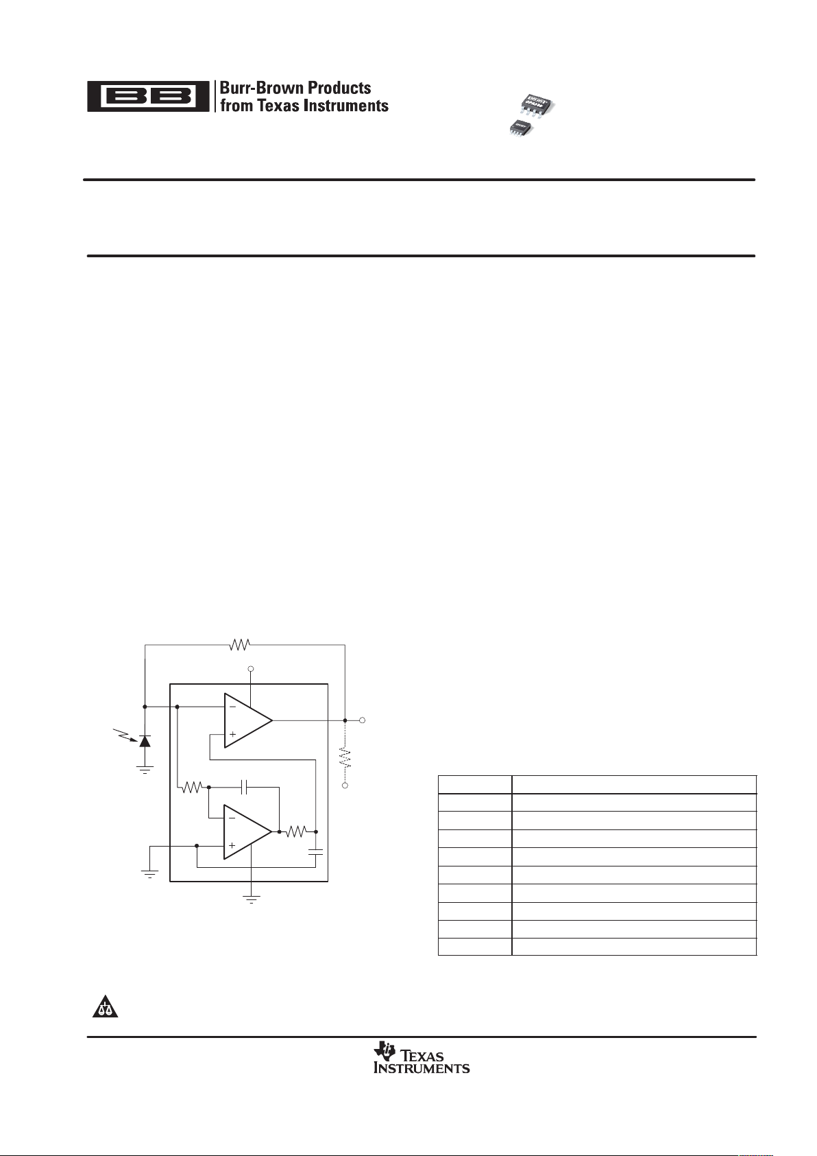
1MΩ
R
F
100kΩ
+5V
7
2
3
4
6
OPA380
67pF
75pF
−5V
R
P
(Optional
Pulldown
Resistor)
V
OUT
(0V to 4.4V)
Photodiode
DESCRIPTION
The OPA380 family of transimpedance amplifiers provides
high-speed (90MHz Gain Bandwidth [GBW]) operation, with
extremely high precision, excellent long-term stability, and
very low 1/f noise. It is ideally suited for high-speed
photodiode applications. The OPA380 features an offset
voltage of 25µV, offset drift of 0.1µV/°C, and bias current of
50pA. The OPA380 far exceeds the offset, drift, and noise
performance that conventional JFET op amps provide.
The signal bandwidth o f a t ransimpedance a mplifier d epends
largely on the GBW of the amplifier and the parasitic
capacitance of the photodiode, as well as the feedback
resistor. The 90MHz GBW of the OPA380 enables a transimpedance bandwidth of > 1 MHz i n most c onfigurations. The
OPA380 is i deally suited f or f ast c ontrol l oops f or p ower l evel
on an optical fiber.
As a result o f t he h igh p r ecision and l ow-noise c haracteristics
of the OPA380, a dynami c range of 4 to 5 dec ades can be
achieved. For example, this capability allows the
measurement of signal currents on the order of 1nA, and up
to 100µA in a single I/V conversion stage. In contrast to
logarithmic amplifiers, the OPA380 provides very wide
bandwidth throughout the full dynamic range. By using an
external pull-down resistor to –5V, the output voltage range
can be extended to include 0V.
The OPA380 (single) is available in MSOP-8 and SO-8
packages. The OPA2380 (dual) is available in the
miniature MSOP-8 package. They are specified from
–40°C to +125°C.
OPA380 RELATED DEVICES
PRODUCT FEATURES
OPA300 150MHz CMOS, 2.7V to 5.5V Supply
OPA350 500µV VOS, 38MHz, 2.5V to 5V Supply
OPA335 10µV VOS, Zero-Drift, 2.5V to 5V Supply
OPA132 16MHz GBW, Precision FET Op Amp, ±15V
OPA656/7 230MHz, Precision FET, ±5V
LOG112 LOG amp, 7.5 decades, ±4.5V to ±18V Supply
LOG114 LOG amp, 7.5 decades, ±2.25V to ±5.5V Supply
IVC102 Precision Switched Integrator
DDC112 Dual Current Input, 20-Bit ADC
OPA380
OPA2380
SBOS291F − NOVEMBER 2003 − REVISED JUNE 2005
Precision, High-Speed
Transimpedance Amplifier
! !
www.ti.com
Copyright 2003-2005, Texas Instruments Incorporated
All trademarks are the property of their respective owners.
Please be aware that an important notice concerning availability, standard warranty, and use in critical applications of Texas Instruments
semiconductor products and disclaimers thereto appears at the end of this data sheet.
"#$
%"#$
SBOS291F − NOVEMBER 2003 − REVISED JUNE 2005
www.ti.com
2
ABSOLUTE MAXIMUM RATINGS
(1)
Voltage Supply +7V. . . . . . . . . . . . . . . . . . . . . . . . . . . . . . . . . . . . . . .
Signal Input Terminals
(2)
, Voltage −0.5V to ( V + ) + 0.5V. . . . . . . . . .
Current ±10mA. . . . . . . . . . . . . . . . . . . . .
Short-Circuit Current
(3)
Continuous. . . . . . . . . . . . . . . . . . . . . . . . .
Operating Temperature Range −40°C to +125°C. . . . . . . . . . . . . . .
Storage Temperature Range −65°C to +150°C. . . . . . . . . . . . . . . . .
Junction Temperature +150°C. . . . . . . . . . . . . . . . . . . . . . . . . . . . . . .
Lead Tem perature (soldering, 10s) +300°C. . . . . . . . . . . . . . . . . . . . .
ESD Rating (Human Body Model) 2000V. . . . . . . . . . . . . . . . . . . . . . .
(1)
Stresses above these ratings may cause permanent damage.
Exposure to absolute maximum conditions for extended periods
may degrade device reliability. These are stress ratings only , an d
functional operation of the device at these or any other conditions
beyond those specified is not implied.
(2)
Input terminals are diode clamped to the power-supply rails. Input
signals that can swing more than 0.5V beyond the supply rails
should be current limited to 10mA or less.
(3)
Short-circuit to ground; one amplifier per package.
ELECTROSTATIC DISCHARGE SENSITIVITY
This integrated circuit can be damaged by ESD. Texas
Instruments recommends that all integrated circuits be
handled with appropriate precautions. Failure to observe
proper handling and installation procedures can cause damage.
ESD damage can range from subtle performance degradation to
complete device failure. Precision integrated circuits may be more
susceptible t o damage because very small parametric changes could
cause the device not to meet its published specifications.
PACKAGE/ORDERING INFORMATION
(1)
PRODUCT PACKAGE-LEAD
PACKAGE
MARKING
OPA380
MSOP-8
AUN
OPA380
SO-8
OPA380A
OPA2380
MSOP-8
BBX
(1)
For the most current package and ordering information, see the
Package Option Addendum at the end of this document, or see
the TI web site at www.ti.com.
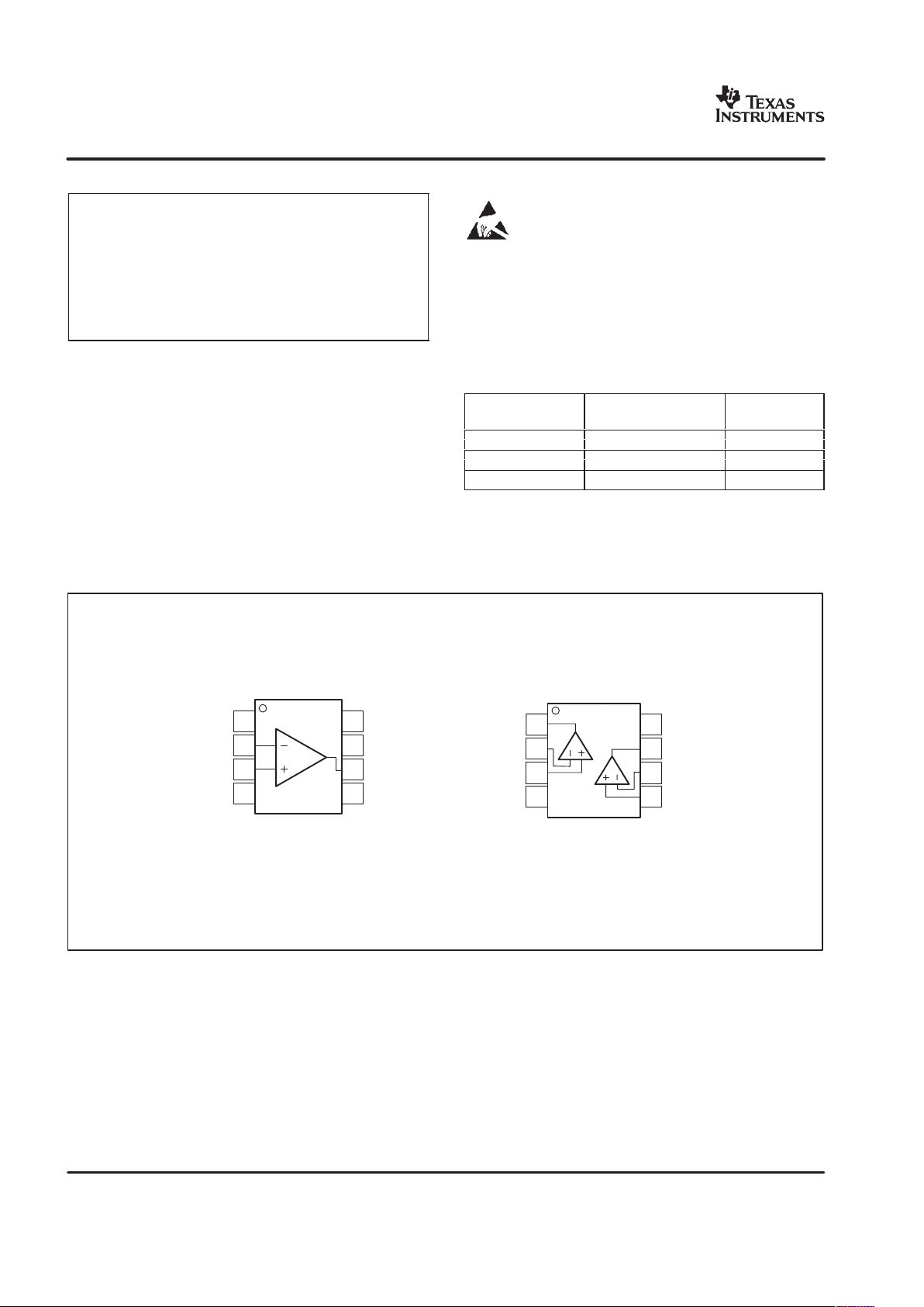
PIN ASSIGNMENTS
Top View
1
2
3
4
8
7
6
5
NC
(1)
V+
Out
NC
(1)
NC
(1)
−
In
+In
V
−
OPA380
MSOP-8, SO-8
NOTES: (1) NCindicates no internal connection.
1
2
3
4
8
7
6
5
V+
Out B
−
In B
+In B
Out A
−
In A
+In A
V
−
OPA2380
MSOP-8

"#$
%"#$
SBOS291F − NOVEMBER 2003 − REVISED JUNE 2005
www.ti.com
3
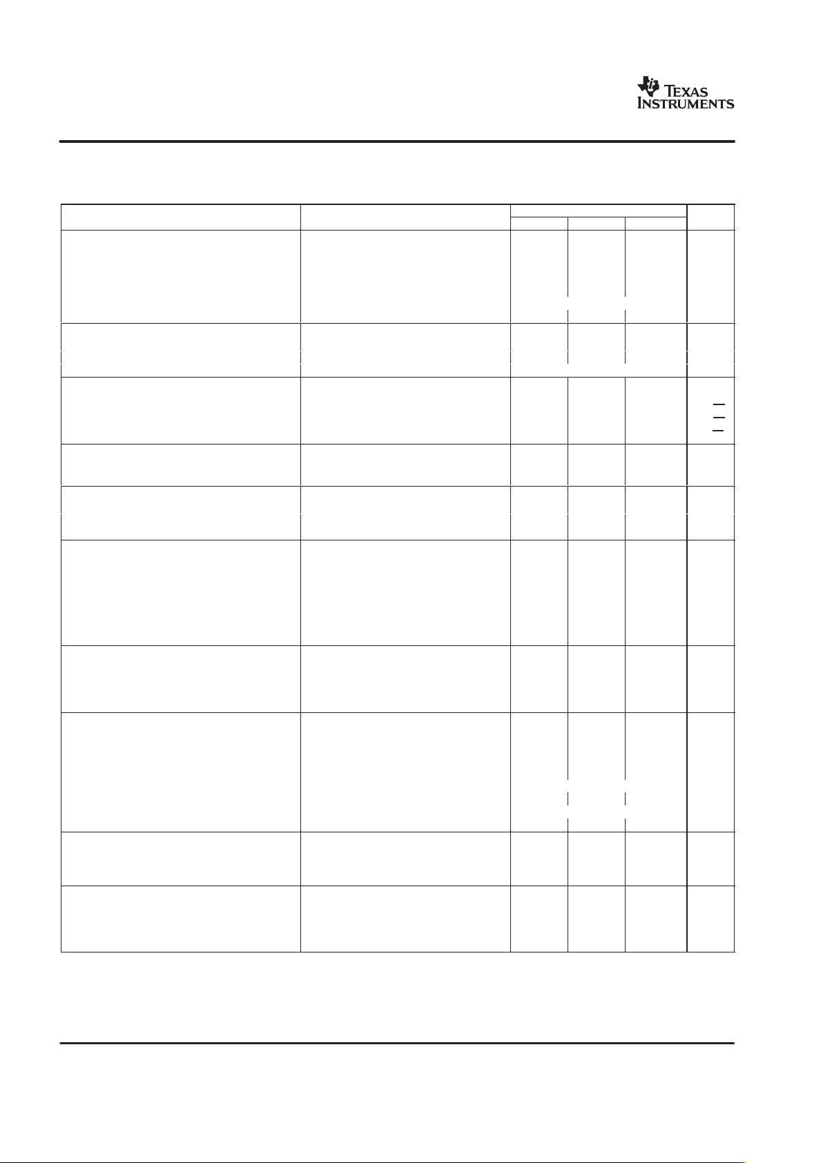
ELECTRICAL CHARACTERISTICS: OPA380 (SINGLE), VS = 2.7V to 5.5V
Boldface limits apply over the temperature range, TA = −40°C to +125°C.
All specifications at TA = +25°C, RL = 2kΩ connected to VS/2, and V
OUT
= VS/2, unless otherwise noted.
OPA380
PARAMETER CONDITION
MIN TYP MAX
UNITS
OFFSET VOLTAGE
Input Offset Voltage V
OS
VS = +5V , VCM = 0V 4 25 µV
Drift dVOS/dT 0.03 0.1 µV/°C
vs Power Supply PSRR VS = +2.7V to +5.5V , VCM = 0V 2.4 10 µV/V
Over Temperature VS = +2.7V to +5.5V , VCM = 0V 10 µV/V
Long-Term Stability
(1)
See Note (1)
Channel Separation, dc 1 µV/V
INPUT BIAS CURRENT
Input Bias Current I
B
VCM = VS/2 3 ±50 pA
Over Temperature Typical Characteristics
Input Offset Current I
OS
VCM = VS/2 6 ±100 pA
NOISE
Input Voltage Noise, f = 0.1Hz to 10Hz e
n
VS = +5V , VCM = 0V 3 µV
PP
Input Voltage Noise Density, f = 10kHz e
n
VS = +5V , VCM = 0V 67 nV/√Hz
Input Voltage Noise Density, f > 1MHz e
n
VS = +5V , VCM = 0V 5.8 nV/√Hz
Input Current Noise Density, f = 10kHz i
n
VS = +5V , VCM = 0V 10 fA/√Hz
INPUT VOLTAGE RANGE
Common-Mode Voltage Range V
CM
V− (V+) − 1.8V V
Common-Mode Rejection Ratio CMRR (V−) < VCM < (V+) – 1.8V 100 110 dB
INPUT IMPEDANCE
Differential Capacitance 1.1 pF
Common-Mode Resistance and Inverting Input
Capacitance
1013 || 3 Ω || pF
OPEN-LOOP GAIN
Open-Loop Voltage Gain AOL0.1V < VO < (V+) − 0.7V , VS = 5V , VCM = VS/2 110 130 dB
0.1V < VO < (V+) − 0.6V , VS = 5V , VCM = VS/2,
T
A
= −40°C to +85°C
110 130 dB
0V < VO < (V+) − 0.7V , VS = 5V , VCM = 0V ,
R
P
= 2kΩ to −5V
(2)
106 120 dB
0V < VO < (V+) − 0.6V , VS = 5V , VCM = 0V ,
R
P
= 2kΩ to −5V
(2)
, TA = −40°C to +85°C
106 120 dB
FREQUENCY RESPONSE CL = 50pF
Gain-Bandwidth Product GBW 90 MHz
Slew Rate SR G = +1 80 V/µs
Settling Time, 0.01%
(3)
t
S
VS = +5V, 4V Step, G = +1 2 µs
Overload Recovery Time
(4)(5)
VIN × G = > V
S
100 ns
OUTPUT
Voltage Output Swing from Positive Rail RL = 2kΩ 400 600 mV
Voltage Output Swing from Negative Rail RL = 2kΩ 60 100 mV
Voltage Output Swing from Positive Rail RP = 2kΩ to −5V
(2)
400 600 mV
Voltage Output Swing from Negative Rail RP = 2kΩ to −5V
(2)
−20 0 mV
Output Current I
OUT
See Typical Characteristics
Short-Circuit Current I
SC
150 mA
Capacitive Load Drive C
LOAD
See Typical Characteristics
Open-Loop Output Impedance R
O
f = 1MHz, IO = 0A 40 Ω
POWER SUPPL Y
Specified Voltage Range V
S
2.7 5.5 V
Quiescent Current I
Q
IO = 0A 6.5 8.3 mA
Over Temperature 8.8 mA
TEMPERATURE RANGE
Specified and Operating Range −40 +125 °C
Storage Range −65 +150 °C
Thermal Resistance q
JA
MSOP-8, SO-8 150 °C/W
(1)
300-hour life test at 150°C demonstrated randomly distributed variation approximately equal to measurement repeatability of 1µV.
(2)
Tested with output connected only to R
P
, a pulldown resistor connected between V
OUT
and −5V , as shown in Figure 5. See also applications section, Achieving
Output Swing to Ground.
(3)
Transimpedance frequency of 1MHz.
(4)
Time required to return to linear operation.
(5)
From positive rail.
"#$
%"#$
SBOS291F − NOVEMBER 2003 − REVISED JUNE 2005
www.ti.com
4
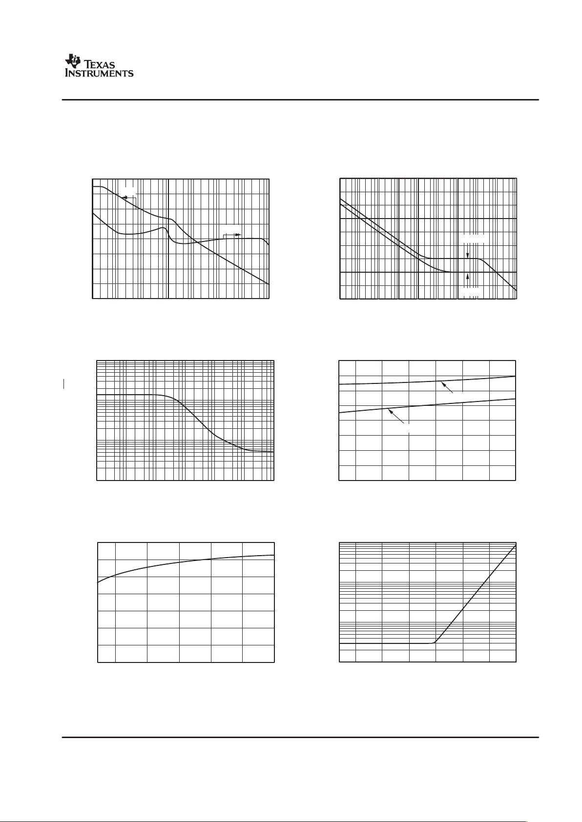
ELECTRICAL CHARACTERISTICS: OPA2380 (DUAL), VS = 2.7V to 5.5V
Boldface limits apply over the temperature range, TA = −40°C to +125°C.
All specifications at TA = +25°C, RL = 2kΩ connected to VS/2, and V
OUT
= VS/2, unless otherwise noted.
OPA2380
PARAMETER CONDITION
MIN TYP MAX
UNITS
OFFSET VOLTAGE
Input Offset Voltage V
OS
VS = +5V , VCM = 0V 4 25 µV
Drift dVOS/dT 0.03 0.1 µV/°C
vs Power Supply PSRR VS = +2.7V to +5.5V , VCM = 0V 2.4 10 µV/V
Over Temperature VS = +2.7V to +5.5V , VCM = 0V 10 µV/V
Long-Term Stability
(1)
See Note (1)
Channel Separation, dc 1 µV/V
INPUT BIAS CURRENT
Input Bias Current, Inverting Input I
B
VCM = VS/2 3 ±50 pA
Noninverting Input I
B
VCM = VS/2 3 ±200 pA
Over Temperature Typical Characteristics
NOISE
Input Voltage Noise, f = 0.1Hz to 10Hz e
n
VS = +5V , VCM = 0V 3 µV
PP
Input Voltage Noise Density, f = 10kHz e
n
VS = +5V , VCM = 0V 67 nV/√Hz
Input Voltage Noise Density, f > 1MHz e
n
VS = +5V , VCM = 0V 5.8 nV/√Hz
Input Current Noise Density, f = 10kHz i
n
VS = +5V , VCM = 0V 10 fA/√Hz
INPUT VOLTAGE RANGE
Common-Mode Voltage Range V
CM
V− (V+) − 1.8V V
Common-Mode Rejection Ratio CMRR (V−) < VCM < (V+) – 1.8V 95 105 dB
INPUT IMPEDANCE
Differential Capacitance 1.1 pF
Common-Mode Resistance and Inverting Input
Capacitance
1013 || 3 Ω || pF
OPEN-LOOP GAIN
Open-Loop Voltage Gain AOL0.12V < VO < (V+) − 0.7V , VS = 5V , VCM = VS/2 110 130 dB
0.12V < VO < (V+) − 0.6V, VS = 5V , VCM = VS/2,
T
A
= −40°C to +85°C
110 130 dB
0V < VO< (V+) − 0.7V , VS = 5V , VCM = 0V ,
R
P
= 2kΩ to −5V
(2)
106 120 dB
0V < VO < (V+) − 0.6V , VS = 5V , VCM = 0V ,
R
P
= 2kΩ to −5V
(2)
, TA = −40°C to +85°C
106 120 dB
FREQUENCY RESPONSE CL = 50pF
Gain-Bandwidth Product GBW 90 MHz
Slew Rate SR G = +1 80 V/µs
Settling Time, 0.01%
(3)
t
S
VS = +5V, 4V Step, G = +1 2 µs
Overload Recovery Time
(4)(5)
VIN × G = > V
S
100 ns
OUTPUT
Voltage Output Swing from Positive Rail RL = 2kΩ 400 600 mV
Voltage Output Swing from Negative Rail RL = 2kΩ 80 120 mV
Voltage Output Swing from Positive Rail RP = 2kΩ to −5V
(2)
400 600 mV
Voltage Output Swing from Negative Rail RP = 2kΩ to −5V
(2)
−20 0 mV
Output Current I
OUT
See Typical Characteristics
Short-Circuit Current I
SC
150 mA
Capacitive Load Drive C
LOAD
See Typical Characteristics
Open-Loop Output Impedance R
O
f = 1MHz, IO = 0A 40 Ω
POWER SUPPL Y
Specified Voltage Range V
S
2.7 5.5 V
Quiescent Current (per amplifier) I
Q
IO = 0A 7.5 9.5 mA
Over Temperature 10 mA
TEMPERATURE RANGE
Specified and Operating Range −40 +125 °C
Storage Range −65 +150 °C
Thermal Resistance q
JA
MSOP-8 150 °C/W
(1)
300-hour life test at 150°C demonstrated randomly distributed variation approximately equal to measurement repeatability of 1µV.
(2)
Tested with output connected only to R
P
, a pulldown resistor connected between V
OUT
and −5V , as shown in Figure 5. See also applications section, Achieving
Output Swing to Ground.
(3)
Transimpedance frequency of 1MHz.
(4)
Time required to return to linear operation.
(5)
From positive rail.
"#$
%"#$
SBOS291F − NOVEMBER 2003 − REVISED JUNE 2005
www.ti.com
5
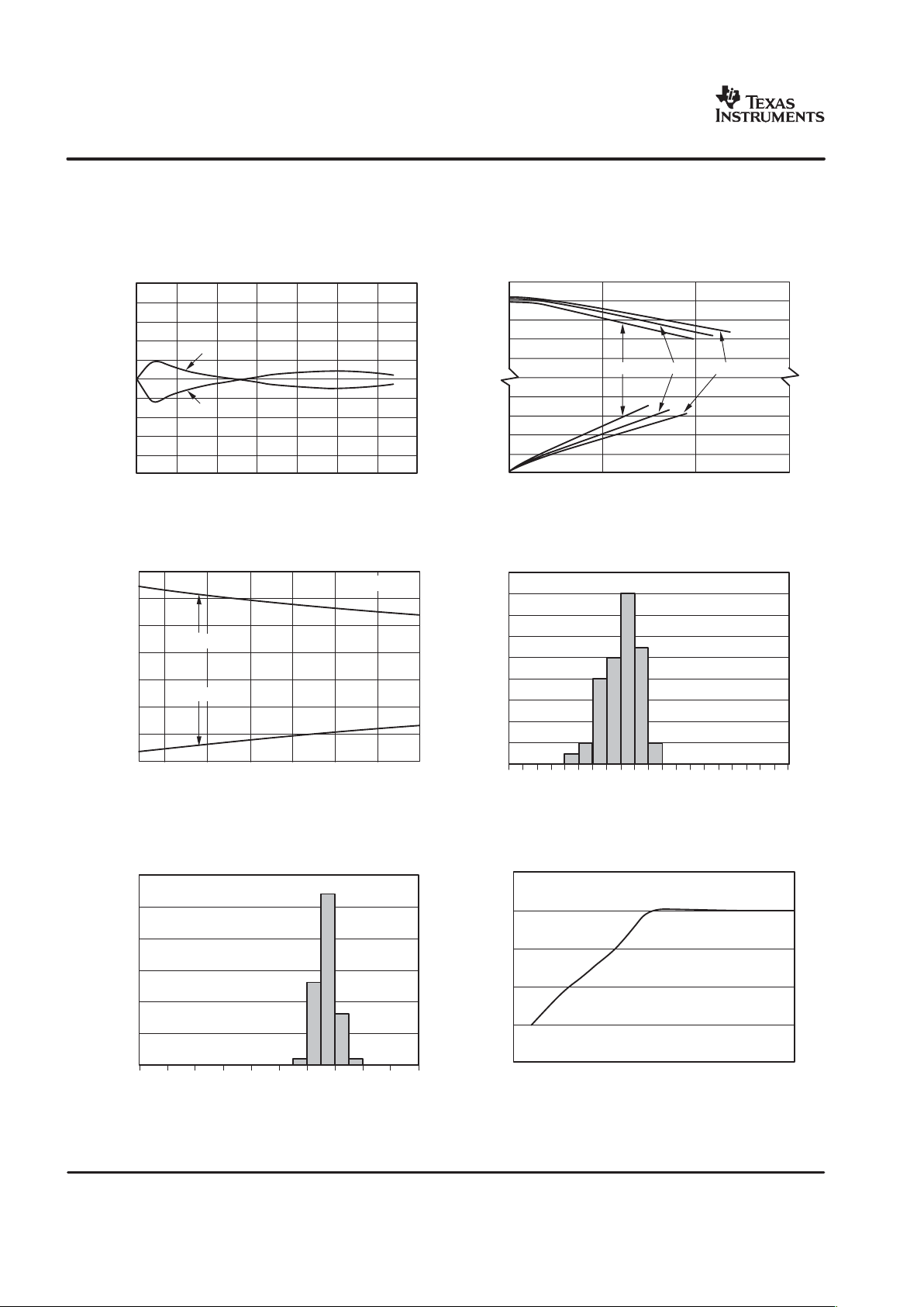
TYPICAL CHARACTERISTICS: VS = +2.7V to +5.5V
All specifications at TA = +25°C, RL = 2kΩ connected to VS/2, and V
OUT
= VS/2, unless otherwise noted.
140
120
100
80
60
40
20
0
−
20
OPEN−LOOPGAIN AND PHASE vs FREQUENCY
Frequency (Hz)
Open−L oop Gain (dB)
90
45
0
−
45
−
90
−
135
−
180
−
225
−
270
Phase (
_
)
10 100 10M1M10k 100k1k 100M
Gain
Phase
160
140
120
100
80
60
40
20
0
−
20
POWER−SUPPLY REJECTION RATIO AND
COMMON−MODE REJECTION vs FREQUENCY
Frequency (Hz)
PSRR, CMRR (dB)
0.1 1 100k 10M1M1k 10k10 100 100M
PSRR
CMRR
1000
100
10
1
INPUT VOLTAGE NOISE SPECTRAL DENSITY
Frequency (Hz)
Input Voltage Noise (nV/
√
(Hz)
10 100 100k 1M10k1k 10M
8
7
6
5
4
3
2
1
0
QUIESCENT CURRENT vs TEMPERATURE
Temperature (_C)
Quiescent Current (mA)
−40−
25 0 25 50 75 100 125
VS=+2.7V
VS=+5.5V
7
6
5
4
3
2
1
0
QUIESCENT CURRENT vs SUPPLY VOLTAGE
Supply Voltage (V)
QuiescentCurrent(mA)
2.7 3.0 3.5 4.0 4.5 5.0 5.5
1000
100
10
1
INPUT BIAS CURRENT vs TEMPERATURE
Temperature (_C)
Input BiasCurrent(pA)
−
40 100 125
−
25 0 25 50 75
"#$
%"#$
SBOS291F − NOVEMBER 2003 − REVISED JUNE 2005
www.ti.com
6
TYPICAL CHARACTERISTICS: VS = +2.7V to +5.5V (continued)
All specifications at TA = +25°C, RL = 2kΩ connected to VS/2, and V
OUT
= VS/2, unless otherwise noted.
25
20
15
10
5
0
−
5
−
10
−
15
−
20
−
25
INPUT BIAS CURRENT
vs INPUT COMMON−MODE VOLTAGE
Input Common−Mode Voltage (V)
−
I
B
+
I
B
Input Bias Current (pA)
0 0.5 1.0 1.5 2.0 2.5 3.0 3.5
OUTPUT VOLTAGE SWING vs OUTPUT CURRENT
+125_C
+25_C−40_C
Output Swing(V)
50 100 1500
(V+)
(V+)−1
(V+)−2
(V−)+2
(V−)+1
(V−)
Output Current (mA)
−
40 100 125
−
250 255075
SHORT−CIRCUIT CURRENT vs TEMPERATURE
Short−Circuit Current(mA)
200
150
100
50
0
−
50
−
100
−
150
Temperature (_C)
VS=5V
+I
SC
−
I
SC
OFFSET VOLTAGE PRODUCTION DISTRIBUTION
Offset Voltage (µV)
−25−20−15−10−
50 5 10152025
Population
OFFSETVOLTAGE DRIFT
PRODUCTION DISTRIBUTION
Offset Voltage Drift (µV/_C)
−
0.10−0.08−0.06−0.04−0.02 0 0.020.040.060.08 0.1
Population
GAIN BANDWIDTH vs POWER SUPPLY VOLTAGE
Gain Bandwidth (MHz)
3.5 4.5 5.52.5
95
90
85
80
75
70
Power Supply Voltage (V)
 Loading...