

6
3
0
–3
–6
–9
–12
–15
–18
–21
–24
Normalized Gain (3dB/div)
RF = 800Ω
G = 100
G = 50
G = 20
G = 10
G = 2
G = 1
10 100 200
BW (MHz) vs GAIN
G = 5
MHz
查询DEM-OPA368XD供应商
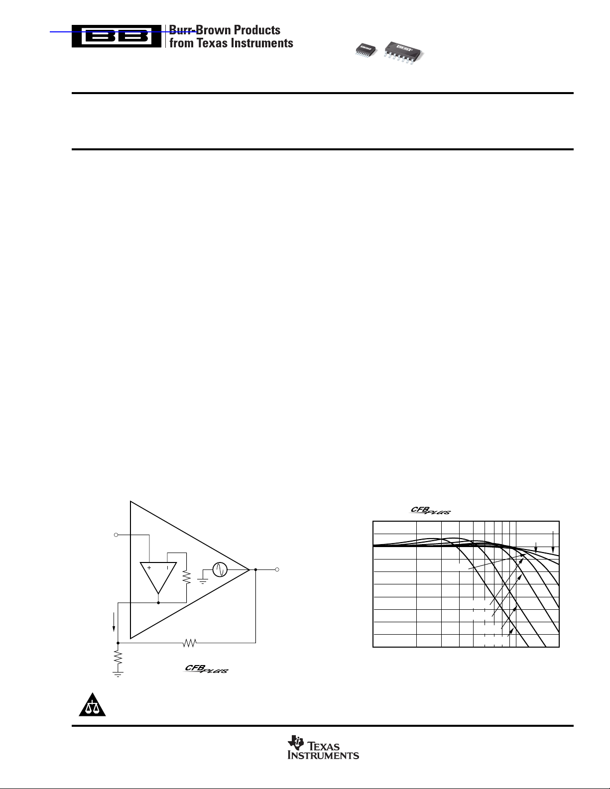
Low-Power, Triple Current-Feedback
OPERATIONAL AMPLIFIER With Disable
O
OPA3684
P
A
3
6
8
4
SBOS241A – MAY 2002 – REVISED SEPTEMBER 2002
FEATURES
● MINIMAL BANDWIDTH CHANGE VERSUS GAIN
● 170MHz BANDWIDTH: G = +2
● > 120MHz BANDWIDTH TO GAIN > +10
● LOW DISTORTION: < –82dBc at 5MHz
● HIGH OUTPUT CURRENT: 120mA
● SINGLE +5V TO +12V SUPPLY OPERATION
● DUAL ±2.5V TO ±6.0V SUPPLY OPERATION
● LOW SUPPLY CURRENT: 1.7mA/ch
● LOW SHUTDOWN CURRENT: 100µA/ch
DESCRIPTION
The OPA3684 provides a new level of performance in low-power,
wideband, current-feedback (CFB) amplifiers. This CFB
plifier among the first to use an internally closed-loop input buffer
stage that enhances performance significantly over earlier lowpower CFB amplifiers. While retaining the benefits of very low
power operation, this new architecture provides many of the
benefits of a more ideal CFB amplifier. The closed-loop input stage
buffer gives a very low and linearized impedance path at the
inverting input to sense the feedback error current. This improved
inverting input impedance retains exceptional bandwidth to much
higher gains and improves harmonic distortion over earlier solutions limited by inverting input linearity. Beyond simple high- gain
applications, the OPA3684 CFB
amplifier permits the gain
PLUS
setting element to be set with considerable freedom from amplifier
bandwidth interaction. This allows frequency response peaking
elements to be added, multiple input inverting summing circuits to
PLUS
am-
APPLICATIONS
● RGB LINE DRIVERS
● LOW-POWER BROADCAST VIDEO DRIVERS
● EQUALIZING FILTERS
● MULTICHANNEL SUMMING AMPLIFIERS
● PROFESSIONAL CAMERAS
● ADC INPUT DRIVERS
have greater bandwidth, and low-power line drivers to meet the
demanding requirements of studio cameras and broadcast video.
The output capability of the OPA3684 also sets a new mark in
performance for low-power current-feedback amplifiers. Delivering
a full ±4Vp-p swing on ±5V supplies, the OPA3684 also has the
output current to support > ±3Vp-p into 50Ω. This minimal output
headroom requirement is complemented by a similar 1.2V input
stage headroom giving exceptional capability for single +5V operation.
The OPA3684’s low 1.7mA/ch supply current is precisely trimmed
at 25°C. This trim, along with low shift over temperature and supply
voltage, gives a very robust design over a wide range of operating
conditions. System power may be further reduced by using the
optional disable control pin. Leaving this disable pin open, or holding
it HIGH, gives normal operation. If pulled LOW, the OPA3684 supply
current drops to less than 100µA/ch while the I/O pins go to a high
impedance state.
V+
V–
I
ERR
PRODUCTION DATA information is current as of publication date.
Products conform to specifications per the terms of Texas Instruments
standard warranty. Production processing does not necessarily include
testing of all parameters.
R
G
Low-Power Amplifier
Please be aware that an important notice concerning availability, standard warranty, and use in critical applications of
Texas Instruments semiconductor products and disclaimers thereto appears at the end of this data sheet.
Patent Pending
1 of 3 Channels
Z
(S)
R
F
+
I
ERR
V
O
Copyright © 2002, Texas Instruments Incorporated
www.ti.com
ABSOLUTE MAXIMUM RATINGS
Power Supply ............................................................................... ±6.5V
Internal Power Dissipation ................................. See Thermal Information
Differential Input Voltage .................................................................. ±1.2V
Input Voltage Range ............................................................................ ±V
Storage Temperature Range: ID, IDBQ ........................ –40°C to +125°C
Lead Temperature (soldering, 10s).............................................. +300°C
Junction Temperature (T
ESD Rating: HBM ............................................................................ 1900V
CDM ........................................................................... 1500V
NOTE: (1) Stresses above these ratings may cause permanent damage.
Exposure to absolute maximum conditions for extended periods may degrade
device reliability.
) ........................................................... +175°C
J
(1)
DC
ELECTROSTATIC
DISCHARGE SENSITIVITY
This integrated circuit can be damaged by ESD. Texas Instru-
S
ments recommends that all integrated circuits be handled with
appropriate precautions. Failure to observe proper handling
and installation procedures can cause damage.
ESD damage can range from subtle performance degradation to
complete device failure. Precision integrated circuits may be more
susceptible to damage because very small parametric changes
could cause the device not to meet its published specifications.
OPA3684 RELATED PRODUCTS
SINGLES DUALS TRIPLES QUADS FEATURES
OPA684 OPA2684 — OPA4684 Low-Power CFB
OPA691 OPA2691 OPA3691 — High Slew Rate CFB
OPA685 ———> 500MHz CFB
OPA692 — OPA3692 — Fixed-Gain Video Buffers
plus
PACKAGE/ORDERING INFORMATION
PRODUCT PACKAGE-LEAD DESIGNATOR
PACKAGE TEMPERATURE PACKAGE ORDERING TRANSPORT
OPA3684 SO-14 D –40°C to +85°C OPA3684 OPA3684ID Rails, 58
(1)
"""""OPA3684IDR Tape and Reel, 2500
OPA3684 SSOP-16 DBQ –40°C to +85°C OPA3684 OPA3684IDBQT Tape and Reel, 250
"""""OPA3684IDBQR Tape and Reel, 2500
NOTE: (1) For the most current specifications, and package information, refer to our web site at www.ti.com.
SPECIFIED
RANGE MARKING NUMBER MEDIA, QUANTITY
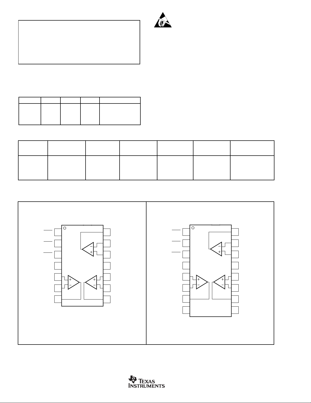
PIN CONFIGURATION
Top View SO
DIS A
DIS B
DIS C
+V
+Input A
–Input A
Output A
1
2
C
3
4
S
5
6
7
14
Output C
13
–Input C
12
+Input C
11
–V
S
10
9
8
+Input B
–Input B
Output B
BA
Top View SSOP
DIS A
DIS B
DIS C
+V
+Input A
–Input A
Output A
NC
1
2
C
3
4
S
5
6
7
8
16
Output C
15
–Input C
14
+Input C
13
–V
S
12
11
10
9
+Input B
–Input B
Output B
NC
BA
2
www.ti.com
OPA3684
SBOS241A
ELECTRICAL CHARACTERISTICS: VS = ±5V
Boldface limits are tested at +25°C.
RF = 800Ω, RL = 100Ω, and G = +2, unless otherwise noted.
OPA3684ID, IDBQ
TYP MIN/MAX OVER TEMPERATURE
PARAMETER CONDITIONS +25°C +25°C
(1)
70°C
(2)
+85°C
(2)
UNITS MAX
0°C to –40°C to
AC PERFORMANCE (see Figure 1)
Small-Signal Bandwidth (VO = 0.5Vp-p) G = +1, RF = 800Ω 250 MHz typ C
G = +2, RF = 800Ω 170 120 118 117 MHz min B
G = +5, RF = 800Ω 138 MHz typ C
G = +10, R
G = +20, R
Bandwidth for 0.1dB Gain Flatness G = +2, VO = 0.5Vp-p, RF = 800Ω 19 16 14 14 MHz min B
= 800Ω 120 MHz typ C
F
= 800Ω 95 MHz typ C
F
Peaking at a Gain of +1 RF = 800Ω, VO = 0.5Vp-p 1.4 4.8 5.9 6.3 dB max B
Large-Signal Bandwidth G = +2, VO = 4Vp-p 90 MHz typ C
Slew Rate G = –1, V
G = +2,V
Rise-and-Fall Time G = +2, VO = 0.5V Step 3 ns typ C
= 4V Step 780 675 650 575 V/µsminB
O
= 4V Step 750 680 660 650 V/µsminB
O
G = +2, VO = 4VStep 6.8 ns typ C
Harmonic Distortion G = +2, f = 5MHz, VO = 2Vp-p
2nd-Harmonic R
3rd-Harmonic RL = 100Ω –70 –66 –65 –65 dBc max B
= 100Ω –67 –59 –59 –58 dBc max B
L
R
≥ 1kΩ –82 –66 –65 –65 dBc max B
L
RL ≥ 1kΩ –84 –82 –81 –81 dBc max B
Input Voltage Noise f > 1MHz 3.7 4.1 4.2 4.4 nV/√Hz max B
Noninverting Input Current Noise f > 1MHz 9.4 11 12 12.5 pA/√Hz max B
Inverting Input Current Noise f > 1MHz 17 18 18.5 19 pA/√Hz max B
Differential Gain G = +2, NTSC, VO = 1.4Vp, RL = 150Ω 0.04 % typ C
Differential Phase G = +2, NTSC, VO = 1.4Vp, RL = 150Ω 0.02 deg typ C
All Hostile Crosstalk 2 Channels, f = 5MHz 70 dB typ C
3rd-Channel Measured
DC PERFORMANCE
Open-Loop Transimpedance Gain (ZOL)
(4)
VO = 0V, RL = 1kΩ 355 160 155 153 kΩ min A
Input Offset Voltage VCM = 0V ±1.5 ±3.9 ±4.5 ±4.7 mV max A
Average Offset Voltage Drift VCM = 0V ±12 ±12 µV/°CmaxB
Noninverting Input Bias Current VCM = 0V ±5.0 ±12 ±13.5 ±14 µAmaxA
Average Noninverting Input Bias Current Drift VCM = 0V ±25 ±30 nA/°CmaxB
Inverting Input Bias Current VCM = 0V ±5.0 ±17 ±18.5 ±19.5 µAmaxA
Average Inverting Input Bias Current Drift VCM = 0V ±35 ±40 nA°/C max B
INPUT
Common-Mode Input Range
(5)
(CMIR) ±3.75 ±3.65 ±3.65 ±3.6 V min A
Common-Mode Rejection Ratio (CMRR) VCM = 0V 60 53 52 52 dB min A
Noninverting Input Impedance 50 || 2 kΩ || pF typ C
Inverting Input Resistance (RI) Open-Loop, DC 4.0 Ω typ C
OUTPUT
Voltage Output Swing 1kΩ Load ±4.1
±3.9 ±3.9 ±3.8 V min A
Current Output, Sourcing VO = 0 160 120 115 110 mA min A
Current Output, Sinking VO = 0 –120 –100 –95 –90 mA min A
Closed-Loop Output Impedance G = +2, f = 100kHz 0.006 Ω typ C
DISABLE (Disabled LOW)
Power-Down Supply Current (+V
Disable Time V
)V
S
Enable Time V
Off Isolation G = +2, 5MHz 70 dB typ C
= 0 (all channels) –300 –500 –580 –600 µAmaxA
DIS
= +1V, G = +2 4 ms typ C
IN
= +1V, G = +2 40 ns typ C
IN
Output Capacitance in Disable 1.7 pF typ C
Enable Voltage 3.4 3.5 3.6 3.7 V min A
Disable Voltage 1.8 1.7 1.6 1.5 V max A
Control Pin Input Bias Current (DIS) V
= 0V/Channel 80 120 130 135 µAmaxA
DIS
POWER SUPPLY
Specified Operating Voltage ±5 V typ C
Maximum Operating Voltage Range
±6 ±6 ±6VmaxA
Max Quiescent Current VS = ±5V/per Channel 1.7 1.8 1.85 1.85 mA max A
Min Quiescent Current VS = ±5V/per Channel 1.7 1.6 1.55 1.45 mA min A
Power-Supply Rejection Ratio (–PSRR) Input Referred 60 54 53 53 dB typ A
TEMPERATURE RANGE
Specification: D, DBQ
Thermal Resistance,
D SO-14 100 °C/W typ C
θ
JA
Junction-to-Ambient
–40 to +85
DBQ SSOP-16 100 °C/W typ C
NOTES: (1) Junction temperature = ambient for +25°C tested specifications. (2) Junction temperature = ambient at low temperature limit, junction temperature = ambient
+2°C at high temperature limit for over temperature tested specifications. (3) Test levels: (A) 100% tested at +25°C. Over-temperature limits by characterization and
simulation. (B) Limits set by characterization and simulation. (C) Typical value only for information. (4) Current is considered positive out-of-node. V
common-mode voltage. (5) Tested < 3dB below minimum specified CMR at ± CMIR limits.
MIN/
TEST
LEVEL
°C typ C
is the input
CM
(3)
OPA3684
SBOS241A
www.ti.com
3
ELECTRICAL CHARACTERISTICS: VS = +5V
Boldface limits are tested at +25°C.
RF = 1.0kΩ, RL = 100Ω, and G = +2, unless otherwise noted.
OPA3684ID, IDBQ
TYP MIN/MAX OVER TEMPERATURE
PARAMETER CONDITIONS +25°C +25°C
(1)
70°C
(2)
+85°C
(2)
UNITS MAX
0°C to –40°C to
AC PERFORMANCE (see Figure 3)
Small-Signal Bandwidth (V
Bandwidth for 0.1dB Gain Flatness G = +2, V
Peaking at a Gain of +1 R
Large-Signal Bandwidth G = 2, V
Slew Rate G = 2, V
Rise-and-Fall Time G = 2, VO = 0.5V Step 4.3 ns typ C
Harmonic Distortion G = 2, f = 5MHz, V
2nd-Harmonic R
3rd-Harmonic RL = 100Ω to VS/2 –65 –64 –63 –63 dBc max B
Input Voltage Noise f > 1MHz 3.7 4.1 4.2 4.4 nV/√Hz max B
= 0.5Vp-p) G = +1, RF = 1.0kΩ 140 MHz typ C
O
G = +2, R
G = +5, R
G = +10, R
G = +20, RF = 1.0kΩ 75 MHz typ C
= 1.0kΩ, VO < 0.5Vp-p 0.5 2.6 3.4 3.7 dB max B
F
G = 2, V
= 1.0kΩ 110 86 85 82 MHz min B
F
= 1.0kΩ 100 MHz min C
F
= 1.0kΩ 90 MHz typ C
F
< 0.5Vp-p, RF = 1.0kΩ 21 12 11 10 MHz min B
O
= 2Vp-p 86 MHz typ C
O
= 2V Step 380 300 290 285 V/µsminB
O
= 2VStep 4.8 ns typ C
O
= 2Vp-p
= 100Ω to VS/2 –65 –60 –59 –59 dBc max B
L
R
≥ 1kΩ to VS/2 –84 –62 –61 –61 dBc max B
L
≥ 1kΩ to VS/2 –74 –70 –70 –69 dBc max B
R
L
O
Noninverting Input Current Noise f > 1MHz 9.4 11 12 12.5 pA/√Hz max B
Inverting Input Current Noise f > 1MHz 17 18 18.5 19 pA/√Hz max B
Differential Gain G = +2, NTSC, V
Differential Phase G = +2, NTSC, VO = 1.4Vp, RL = 150Ω 0.07 deg typ C
= 1.4Vp, RL = 150Ω 0.04 % typ C
O
All Hostile Crosstalk 2 Channels, f = 5MHz 70 dB typ C
3rd-Channel Measured
DC PERFORMANCE
Open-Loop Transimpedance Gain (ZOL)
(4)
VO = VS/2, RL = 100Ω to VS/2 355 160 155 153 kΩ min A
Input Offset Voltage VCM = VS/2 ±1.0 ±3.4 ±4.0 ±4.2 mV max A
Average Offset Voltage Drift VCM = VS/2 ±12 ±12 µV/°CmaxB
Noninverting Input Bias Current VCM = VS/2 ±5 ±12 ±13.5 ±14 µAmaxA
Average Noninverting Input Bias Current Drift VCM = VS/2 ±25 ±30 nA/°CmaxB
Inverting Input Bias Current VCM = VS/2 ±5 ±13 ±14.5 ±16 µAmaxA
Average Inverting Input Bias Current Drift VCM = VS/2 ±25 ±30 nA°/C max B
INPUT
Least Positive Input Voltage
Most Positive Input Voltage
(5)
(5)
1.25 1.32 1.35 1.38 V max A
3.75 3.68 3.65 3.62 V min A
Common-Mode Refection Ratio (CMRR) VCM = VS/2 58 51 50 50 dB min A
Noninverting Input Impedance 50 || 1 kΩ || pF typ C
Inverting Input Resistance
(RI)
Open-Loop 4.5 Ω typ C
OUTPUT
Most Positive Output Voltage R
Least Positive Output Voltage RL = 1kΩ to VS/2 0.9 1.1 1.1 1.2 V max A
= 1kΩ to VS/2 4.10 3.9 3.9 3.8 V min A
L
Current Output, Sourcing VO = VS/2 80 65 60 55 mA min A
Current Output, Sinking VO = VS/2 70 55 50 45 mA min A
Closed-Loop Output Impedance G = +2, f = 100kHz Ω typ C
DISABLE (Disabled LOW)
Power-Down Supply Current (+V
Off Isolation F = 5.0MHz 70 dB typ C
)V
S
= 0 (all channels) –300 µA typ C
DIS
Output Capacitance in Disable 1.7 pF typ C
Turn-On Glitch G = +2, RL = 150Ω, VIN = VS/2 mV typ C
Turn-Off Glitch G = +2, RL = 150Ω, V
Enable Voltage 3.4 3.5 3.6 3.7 V min A
= VS/2 mV typ C
IN
Disable Voltage 1.8 1.7 1.6 1.5 V max A
Control Pin Input Bias Current (DIS) V
= 0V/Channel 80 120 130 135 µAmaxA
DIS
POWER SUPPLY
Specified Single-Supply Operating Voltage 5 V typ C
Max Single-Supply Operating Voltage Range 12 12 12 V max A
Max Quiescent Current V
Min Quiescent Current VS = +5V/Channel 1.44 1.30 1.20 1.15 mA min A
= +5V/Channel 1.44 1.55 1.55 1.55 mA max A
S
Power-Supply Rejection Ratio (+PSRR) Input Referred 65 dB typ C
TEMPERATURE RANGE
Specification: D, DBQ
Thermal Resistance,
D SO-14 100 °C/W typ C
θ
Junction-to-Ambient
JA
–40 to +85
DBQ SSOP-16 100 °C/W typ C
NOTES: (1) Junction temperature = ambient for +25°C tested specifications. (2) Junction temperature = ambient at low temperature limit, junction temperature = ambient
+1°C at high temperature limit for over temperature tested specifications. (3) Test levels: (A) 100% tested at +25°C. Over-temperature limits by characterization and
simulation. (B) Limits set by characterization and simulation. (C) Typical value only for information. (4) Current is considered positive out-of-node. V
common-mode voltage. (5) Tested < 3dB below minimum specified CMR at ± CMIR limits.
MIN/
TEST
LEVEL
°C typ C
is the input
CM
(3)
4
www.ti.com
OPA3684
SBOS241A
TYPICAL CHARACTERISTICS: VS = ±5V
At TA = +25°C, G = +2, RF = 800Ω, and RL = 100Ω, unless otherwise noted.
NONINVERTING SMALL-SIGNAL
6
VO = 0.5Vp-p
R
= 800Ω
3
F
0
–3
–6
–9
–12
Normalized Gain (3dB/div)
–15
See Figure 1
–18
1 20010 100
9
G = +2
R
= 100Ω
L
6
FREQUENCY RESPONSE
G = 5
G = 10
G = 20
G = 50
G = 100
Frequency (MHz)
NONINVERTING LARGE-SIGNAL
FREQUENCY RESPONSE
G = 1
G = 2
VO = 0.5Vp-p
3
0
–3
–6
–9
Normalized Gain (3dB/div)
–12
3
0
INVERTING SMALL-SIGNAL FREQUENCY RESPONSE
VO = 0.5Vp-p
R
= 800Ω
F
G = –1
G = –2
G = –5
G = –10
See Figure 2
1 20010 100
Frequency (MHz)
INVERTING LARGE-SIGNAL FREQUENCY RESPONSE
G = –1
R
= 100Ω
L
G = –16
VO = 0.5Vp-p
1Vp-p
VO = 1Vp-p
3
Gain (dB)
0
See Figure 1
–3
1 20010 100
Frequency (MHz)
0.8
0.6
0.4
0.2
0
–0.2
–0.4
Output Voltage (200mV/div)
–0.6
–0.8
NONINVERTING PULSE RESPONSE
G = +2
Large-Signal Right Scale
Small-Signal Left Scale
See Figure 1
Time (10ns/div)
VO = 2Vp-p
VO = 5Vp-p
1.6
1.2
0.8
0.4
0
–0.4
–0.8
Output Voltage (400mV/div)
–1.2
–1.6
–3
Gain (dB)
–6
–9
See Figure 2
–12
1 20010 100
Frequency (MHz)
0.8
0.6
0.4
0.2
0
–0.2
–0.4
Output Voltage (200mV/div)
–0.6
See Figure 2
–0.8
INVERTING PULSE RESPONSE
G = –1
Small-Signal Left Scale
Large-Signal Right Scale
Time (10ns/div)
2Vp-p
5Vp-p
1.6
1.2
0.8
0.4
0
–0.4
–0.8
Output Voltage (400mV/div)
–1.2
–1.6
OPA3684
SBOS241A
www.ti.com
5
TYPICAL CHARACTERISTICS: VS = ±5V (Cont.)
At TA = +25°C, G = +2, RF = 800Ω, and RL = 100Ω, unless otherwise noted.
–50
–55
–60
–65
–70
–75
–80
Harmonic Distortion (dBc)
–85
–90
–50
–60
–70
–80
Harmonic Distortion (dBc)
HARMONIC DISTORTION vs LOAD RESISTANCE
VO = 2Vp-p
f = 5MHz
G = +2
2nd-Harmonic
3rd-Harmonic
See Figure 1
100 1k
HARMONIC DISTORTION vs OUTPUT VOLTAGE
f = 5MHz
R
= 100Ω
L
Load Resistance (Ω)
2nd-Harmonic
3rd-Harmonic
–50
–60
–70
–80
Harmonic Distortion (dBc)
–90
–50
–60
–70
–80
Harmonic Distortion (dBc)
HARMONIC DISTORTION vs FREQUENCY
VO = 2Vp-p
R
= 100Ω
L
2nd-Harmonic
3rd-Harmonic
See Figure 1
0.1 20110
Frequency (MHz)
5MHz HARMONIC DISTORTION vs SUPPLY VOLTAGE
VO = 2Vp-p
R
= 100Ω
L
2nd-Harmonic
3rd-Harmonic
–90
0.5 1 5
HARMONIC DISTORTION vs NONINVERTING GAIN
–50
–55
–60
–65
–70
–75
–80
Harmonic Distortion (dBc)
–85
–90
11020
Output Voltage (Vp-p)
2nd-Harmonic
3rd-Harmonic
Noninverting Gain (V/V)
–90
±2.5 ±3 ±3.5 ±4 ±4.5 ±5 ±5.5 ±6
–50
–55
–60
–65
–70
–75
–80
Harmonic Distortion (dBc)
–85
–90
11020
Supply Voltage (±V)
HARMONIC DISTORTION vs INVERTING GAIN
2nd-Harmonic
3rd-Harmonic
Inverting Gain (V/V)
6
www.ti.com
OPA3684
SBOS241A
TYPICAL CHARACTERISTICS: VS = ±5V (Cont.)
2-TONE, 3RD-ORDER
INTERMODULATION DISTORTION
–8 –7 –6 –5 –4 –3 –2 –1453210678
Power at Load (each tone, dBm)
3rd-Order Spurious Level (dBc)
–50
–60
–70
–80
–90
50Ω
+5V
–5V
50Ω
50Ω
P
I
P
O
800Ω
800Ω
OPA3684
20MHz
10MHz
5MHz
1MHz
9
6
3
0
–3
–6
Frequency (MHz)
1 30010 100
SMALL-SIGNAL BANDWIDTH vs C
LOAD
Normalized Gain (dB)
5pF
800Ω
1kΩ
OPA3684
R
S
V
O
+5V
–5V
50Ω
C
L
800Ω
V
I
12pF
100pF
50pF
75pF
20pF
33pF
At TA = +25°C, G = +2, RF = 800Ω, and RL = 100Ω, unless otherwise noted.
INPUT VOLTAGE AND CURRENT NOISE DENSITY
100
Inverting Current Noise
17pA/√Hz
10
Current Noise (pA/√Hz)
Voltage Noise (nV/√Hz)
1
100 10M1k 10k 100k 1M
Noninverting Current Noise
9.4pA/√Hz
Voltage Noise
3.7nV/√Hz
Frequency (Hz)
6
DISABLE TIME
V
DIS
5
4
(V)
DIS
and V
OUT
V
3
V
OUT
2
V
IN = 1VDC
See Figure 1
1
0
01624 86121410
Time (ms)
vs C
R
S
50
LOAD
40
30
(Ω)
S
R
20
10
0
1 10010
OPA3684
SBOS241A
(pF)
C
LOAD
0.5dB Peaking
www.ti.com
–40
G = +2
V
= 0
DIS
–50
–60
–70
DISABLED FEEDTHROUGH
–80
Feedthrough (dB)
–90
–100
See Figure 1
0.1 100110
Frequency (MHz)
7
TYPICAL CHARACTERISTICS: VS = ±5V (Cont.)
At TA = +25°C, G = +2, RF = 800Ω, and RL = 100Ω, unless otherwise noted.
70
CMRR
60
CMRR and PSRR vs FREQUENCY
50
+PSRR
40
30
20
10
Power-Supply Rejection Ratio (dB)
Common-Mode Rejection Ratio (dB)
0
2
10
3
10
4
10
COMPOSITE VIDEO DIFFERENTIAL GAIN/PHASE
0.10
0.09
0.08
Gain = +2
NTSC, Positive Video
0.07
0.06
dG
0.05
0.04
0.03
Differential Gain (%)
Differential Phase (°)
0.02
dP
0.01
0
1423
Number of 150Ω Video Loads
–PSRR
5
10
Frequency (Hz)
OPEN-LOOP TRANSIMPEDANCE GAIN AND PHASE
vs FREQUENCY
120
0
20log (ZOL)
100
80
60
40
∠ Z
OL
–30
–60
–90
–120
Open-Loop Phase (°)
20
Open-Loop Transimpedance Gain (dBΩ)
0
6
10
7
10
8
10
2
10
10310410510610710810
–150
–180
9
Frequency (Hz)
OUTPUT CURRENT AND VOLTAGE LIMITATIONS
5
1W Power
Limit
4
3
2
= 100
L
R
Ω
Ω
0
5
=
L
R
1
(V)
0
O
V
–1
–2
–3
Each
–4
Channel
–5
Ω
= 500
L
R
1W Power
Limit
–150 –100 –50 0 50 100 150
I
(MA)
O
Input Bias Currents (µA)
8
TYPICAL DC DRIFT OVER AMBIENT TEMPERATURE
4
3
2
1
0
Input Offset VoltageNoninverting Input Bias Current
–1
–2
and Offset Voltage (mV)
Inverting Input Bias Current
–3
–4
–50 –25 0 25 50 75 100 125
Ambient T emperature (°C)
www.ti.com
SUPPLY AND OUTPUT CURRENT
200
vs AMBIENT TEMPERATURE
Sourcing Output Current
175
Supply Current
150
Output Current (mA)
125
Sinking Output Current
100
–25 0 25 50 75 100 125
Ambient T emperature (°C)
1.9
1.8
1.7
1.6
Supply Current per Channel (mA)
1.5
OPA3684
SBOS241A

TYPICAL CHARACTERISTICS: VS = ±5V (Cont.)
At TA = +25°C, G = +2, RF = 800Ω, and RL = 100Ω, unless otherwise noted.
Right Scale
SETTLING TIME
Time (ns)
See Figure 1
Input Voltage
Left Scale
Time (100ns/div)
0.05
0.04
0.03
0.02
0.01
–0.01
–0.02
% Error to Final Value
–0.03
–0.04
–0.05
4.0
3.2
2.4
1.6
0.8
–0.8
–1.6
Input Voltage (0.8V/div)
–2.4
–3.2
–4.0
2V Step
See Figure 1
0
0102030405060
NONINVERTING OVERDRIVE RECOVERY
0
Output Voltage
8.0
6.4
4.8
3.2
1.6
0
–1.6
–3.2
–4.8
–6.4
–8.0
–20
–25
2-Channels, 100Ω Load
–30
–35
–40
–45
–50
–55
–60
Crosstalk (Input referred) (dB)
–65
–70
8.0
6.4
4.8
3.2
1.6
0
–1.6
–3.2
Input Voltage (1.6V/div)
Output Voltage (1.6V/div)
–4.8
–6.4
–8.0
ALL HOSTILE CROSSTALK
1Vp-p Output
1010.1 100
Frequency (MHz)
INVERTING OVERDRIVE RECOVERY
Output Voltage
Right Scale
Input Voltage
Left Scale
Time (100ns/div)
See Figure 2
8.0
6.4
4.8
3.2
1.6
0
–1.6
–3.2
–4.8
–6.4
–8.0
Output Voltage (1.6V/div)
6
5
4
3
2
1
0
–1
–2
–3
–4
Input and Output Voltage Range
–5
–6
OPA3684
SBOS241A
INPUT AND OUTPUT VOLTAGE RANGE
vs SUPPLY VOLTAGE
Input
Voltage
Range
Supply Voltage (±V)
Output
Voltage
Range
± 4± 3± 2 ± 5 ± 6
www.ti.com
Output Impedance (Ω)
CLOSED-LOOP OUTPUT IMPEDANCE vs FREQUENCY
100
1/3
10
1
0.01
0.001
OPA3684
800Ω
800Ω
Z
O
100k 1M1k 10k100 10M 100M
Frequency (Hz)
9

TYPICAL CHARACTERISTICS: VS = +5V
At TA = +25°C, G = +2, RF = 1kΩ, and RL = 100Ω, unless otherwise noted.
NONINVERTING SMALL-SIGNAL
6
RF = 1kΩ
3
0
–3
–6
–9
–12
Normalized Gain (3dB/div)
–15
See Figure 3
–18
1 20010 100
FREQUENCY RESPONSE
G = 50
G = 100
G = 20
G = 10
G = 5
Frequency (MHz)
G = 1
G = 2
3
0
–3
–6
–9
Normalized Gain (3dB/div)
–12
INVERTING SMALL-SIGNAL FREQUENCY RESPONSE
RF = 1.0kΩ
G = –1
G = –2
G = –5
G = –10
See Figure 4
1 20010 100
Frequency (MHz)
G = –20
NONINVERTING LARGE-SIGNAL
9
6
3
Gain (dB)
0
–3
1 20010 100
0.4
0.3
0.2
0.1
0
–0.1
–0.2
Output Voltage (200mV/div)
–0.3
See Figure 3.
–0.4
FREQUENCY RESPONSE
0.2Vp-p
Frequency (MHz)
NONINVERTING PULSE RESPONSE
Large-Signal Right Scale
Small-Signal Left Scale
Time (10ns/div)
1Vp-p
0.5Vp-p
2Vp-p
1.6
1.2
0.8
0.4
0
–0.4
–0.8
Output Voltage (400mV/div)
–1.2
–1.6
INVERTING LARGE-SIGNAL FREQUENCY RESPONSE
3
0
–3
Gain (dB)
–6
–9
–12
1 20010 100
Frequency (MHz)
0.4
0.3
0.2
0.1
0
–0.1
–0.2
Output Voltage (200mV/div)
–0.3
See Figure 4
–0.4
INVERTING PULSE RESPONSE
Small-Signal Left Scale
Large-Signal Right Scale
Time (10ns/div)
VO = 0.2Vp-p
VO = 1Vp-p
VO = 2Vp-p
VO = 0.5Vp-p
1.6
1.2
0.8
0.4
0
–0.4
–0.8
Output Voltage (400mV/div)
–1.2
–1.6
10
www.ti.com
OPA3684
SBOS241A

TYPICAL CHARACTERISTICS: VS = +5V (Cont.)
0.16
0.14
0.12
0.10
0.08
0.06
0.04
0.02
0
Number of 150Ω Video Loads
1423
COMPOSITE VIDEO DIFFERENTIAL GAIN/PHASE
Differential Gain (%)
Differential Phase (°)
dP
dG
G = +2
NTSC, Positive Video
At TA = +25°C, G = +2, RF = 1kΩ, and RL = 100Ω, unless otherwise noted.
–50
–55
–60
–65
–70
–75
–80
Harmonic Distortion (dBc)
–85
–90
–50
–60
–70
HARMONIC DISTORTION vs LOAD RESISTANCE
VO = 2Vp-p
f = 5MHz
3rd-Harmonic
2nd-Harmonic
See Figure 3
100 1k
Load Resistance (Ω)
HARMONIC DISTORTION vs OUTPUT VOLTAGE
2nd-Harmonic
3rd-Harmonic
–50
–60
–70
–80
Harmonic Distortion (dBc)
–90
–50
–60
–70
HARMONIC DISTORTION vs FREQUENCY
VO = 2Vp-p
R
= 100Ω
L
2nd-Harmonic
3rd-Harmonic
See Figure 3
0.1 20110
Frequency (MHz)
2-TONE, 3RD-ORDER
INTERMODULATION DISTORTION
20MHz
10MHz
5MHz
–80
Harmonic Distortion (dBc)
See Figure 3
–90
0.5 312
SUPPLY AND OUTPUT CURRENT
100
90
80
70
60
Supply and Output Current (mA)
50
–50 –25 0 25 50 75 125
OPA3684
SBOS241A
Output Voltage (Vp-p)
vs AMBIENT TEMPERATURE
Right-Scale
Supply Current
Sourcing Output Current
Sinking Output Current
Ambient T emperature (°C)
Left-Scale
Left-Scale
100
–80
3rd-Order Spurious Level (dBc)
–90
1.5
1.4
1.3
1.2
1.1
Supply Current per Channel (nA)
1.0
www.ti.com
See Figure 3
–15 –14 –13 –12 –11 –10 –6 –5–7–8–9 –4 –3
Power at Load (each tone, dBm)
11

APPLICATIONS INFORMATION
LOW-POWER, CURRENT-FEEDBACK OPERATION
The triple-channel OPA3684 gives a new level of performance in low-power, current-feedback op amps. Using a
new input stage buffer architecture, the OPA3684 CFB
amplifier holds nearly constant AC performance over a wide
gain range. This closed-loop internal buffer gives a very low
and linearized impedance at the inverting node, isolating the
amplifier’s AC performance from gain element variations.
This allows both the bandwidth and distortion to remain
nearly constant over gain, moving closer to the ideal currentfeedback performance of gain bandwidth independence.
This low-power amplifier also delivers exceptional output
power—it’s ±4V swing on ±5V supplies with > 100mA output
drive gives excellent performance into standard video loads
or doubly-terminated 50Ω cables. Single +5V supply operation is also supported with similar bandwidths but with reduced output power capability. For lower quiescent power in
a CFB
amplifier, consider the OPA683 family; while for
PLUS
higher output power, consider the OPA691 family.
Figure 1 shows the DC-coupled, gain of +2, dual power-
supply circuit used as the basis of the ±5V Electrical and
Typical Characteristics for each channel. For test purposes,
the input impedance is set to 50Ω with a resistor to ground
and the output impedance is set to 50Ω with a series output
resistor. Voltage swings reported in the Electrical Characteristics are taken directly at the input and output pins while load
powers (dBm) are defined at a matched 50Ω load. For
the circuit of Figure 1, the total effective load will be
100Ω || 1600Ω = 94Ω. Gain changes are most easily accomplished by simply resetting the R
value, holding RF constant
G
at its recommended value of 800Ω.
PLUS
mode signal across the input stage, the slew rate for inverting
operation is typically higher and the distortion performance is
slightly improved. An additional input resistor, R
, is included
M
in Figure 2 to set the input impedance equal to 50Ω. The
parallel combination of R
and RG set the input impedance.
M
As the desired gain increases for the inverting configuration,
R
is adjusted to achieved the desired gain, while RM is also
G
adjusted to hold a 50Ω input match. A point will be reached
where R
is set by R
50Ω, increasing R
will equal 50Ω, RM is removed, and the input match
G
only. With RG fixed to achieve an input match to
G
will increase the gain. This will, however,
F
quickly reduce the achievable bandwidth as the feedback
resistor increases from its recommended value of 800Ω. If
the source does not require an input match to 50Ω, either
adjust R
to get the desired load, or remove it and let the R
M
resistor alone provide the input load.
+5V
+
DIS
50Ω
50Ω Load
+
50Ω Source
V
I
R
800Ω
R
M
53.6Ω
0.1µF 6.8µF
1/3
OPA3684
–5V
R
F
800Ω
0.1µF 6.8µF
G
G
+5V
V
I
50Ω Source
R
M
50Ω
R
G
800Ω
1/3
OPA3684
R
800Ω
–5V
0.1µF 6.8µF
F
0.1µF 6.8µF
DIS
+
50Ω
50Ω Load
+
FIGURE 1. DC-Coupled, G = +2V/V, Bipolar Supply Speci-
fications and Test Circuit.
Figure 2 shows the DC-coupled, gain of –1V/V, dual powersupply circuit used as the basis of the Inverting Typical
Characteristics for each channel. Inverting operation offers
several performance benefits. Since there is no common-
FIGURE 2. DC-Coupled, G = –1V/V, Bipolar Supply Specifi-
cations and Test Circuit.
These circuits show ±5V operation. The same circuits can be
applied with bipolar supplies from ±2.5V to ±6V. Internal
supply independent biasing gives nearly the same performance for the OPA3684 over this wide range of supplies.
Generally, the optimum feedback resistor value (for nominally flat frequency response at G = +2) will increase in value
as the total supply voltage across the OPA3684 is reduced.
See Figure 3 for the AC-coupled, single +5V supply, gain of
+2V/V circuit configuration used as a basis for the +5V only
Electrical and Typical Characteristics for each channel. The
key requirement of broadband single-supply operation is to
maintain input and output signal swings within the usable
voltage ranges at both the input and the output. The circuit
of Figure 3 establishes an input midpoint bias using a simple
resistive divider from the +5V supply (two 10kΩ resistors) to
the noninverting input. The input signal is then AC-coupled
into this midpoint voltage bias. The input voltage can swing
to within 1.25V of either supply pin, giving a 2.5Vp-p input
signal range centered between the supply pins. The input
impedance of Figure 3 is set to give a 50Ω input match. If the
source does not require a 50Ω match, remove this and drive
12
www.ti.com
OPA3684
SBOS241A

directly into the blocking capacitor. The source will then see
R
F
1.0kΩ
1/3
OPA3684
+5V
50Ω
50Ω Load
50Ω Source
0.1µF
0.1µF
6.8µF
+
R
G
1.0kΩ
10kΩ
10kΩ
0.1µF
V
I
0.1µF
R
M
52.3Ω
DIS
the 5kΩ load of the biasing network as a load. The gain
resistor (R
) is AC-coupled, giving the circuit a DC gain of +1,
G
which puts the noninverting input DC bias voltage (2.5V) on
the output as well. The feedback resistor value has been
adjusted from the bipolar ±5V supply condition to re-optimize
for a flat frequency response in +5V only, gain of +2,
operation. On a single +5V supply, the output voltage can
swing to within 1.0V of either supply pin while delivering more
than 70mA output current—easily giving a 3Vp-p output
swing into 100Ω (8dBm maximum at the matched 50Ω load).
The circuit of Figure 3 shows a blocking capacitor driving into
a 50Ω output resistor, then into a 50Ω load. Alternatively, the
blocking capacitor could be removed if the load is tied to a
supply midpoint or to ground if the DC current then required
by the load is acceptable.
+5V
The circuits of Figure 3 and 4 show single-supply operation
at +5V. These same circuits may be used up to single
supplies of +12V with minimal change in the performance of
the OPA3684.
+
1/3
OPA3684
1kΩ
0.1µF 6.8µF
DIS
0.1µF
R
F
50Ω Source
V
I
0.1µF
R
M
50Ω
10kΩ
10kΩ
R
G
1kΩ
0.1µF
FIGURE 3. AC-Coupled, G = +2V/V, Single-Supply Specifi-
cations and Test Circuit.
Figure 4 shows the AC-coupled, single +5V supply, gain of
–1V/V circuit configuration used as a basis for the inverting
+5V only Typical Characteristics for each channel. In this
case, the midpoint DC bias on the noninverting input is also
decoupled with an additional 0.1µF capacitor. This reduces
the source impedance at higher frequencies for the
noninverting input bias current noise. This 2.5V bias on the
noninverting input pin appears on the inverting input pin and,
since R
is DC-blocked by the input capacitor, will also
G
appear at the output pin. One advantage to inverting operation is that since there is no signal swing across the input
stage, higher slew rates and operation to even lower supply
voltages is possible. To retain a 1Vp-p output capability,
operation down to a 3V supply is allowed. At a +3V supply,
the input stage is saturated, but for the inverting configuration
of a current-feedback amplifier, wideband operation is retained even under this condition.
OPA3684
SBOS241A
50Ω
50Ω Load
FIGURE 4. AC-Coupled, G = –1V/V, Single-Supply Specifi-
LOW-POWER, VIDEO LINE DRIVER APPLICATIONS
For low-power, video line driving, the OPA3684 provides the
output current and linearity to support 3 channels of either
single video lines, or up to 4 video lines in parallel on each
output. Figure 5 shows a typical ±5V supply video line driver
application where only one channel is shown and only a
single line is being driven. The improved 2nd-harmonic
distortion of the CFB
OPA3684’s high output current and voltage, gives exceptional differential gain and phase performance for a lowpower solution. As the Typical Characteristics show, a single
video load shows a dG/dP of 0.04%/0.02°. Multiple loads
may be driven on each output, with minimal x-talk, while the
dG/dP is still < 0.1%/0.1° for up to 4 parallel video loads. The
slew rate and gain of 2 bandwidth are also suitable to
moderate resolution RGB applications.
FIGURE 5. Noninverting Differential I/O Amplifier.
www.ti.com
VIDEO
cations and Test Circuit.
PLUS
+5V
IN
75Ω
OPA3684
1kΩ
1kΩ
–5V
architecture, along with the
DIS
Supply decoupling not shown.
75Ω
Coax
75Ω Load
13

LOW-POWER RGB MUX/LINE DRIVER
Using the shutdown feature, two OPA3684’s can provide an
easy low-power way to select one of two possible RGB
sources for moderate resolution monitors. Figure 6 shows a
recommended circuit where each of the color outputs are
combined in a way that provides a net gain of 1 to the
matched 75Ω load with a 75Ω output impedance. This brings
the two outputs for each color together through a 78.7Ω
resistor with a slightly > 2 gain provided by the amplifiers.
+5V
V
DIS
+5V
R1
75Ω
681Ω 806Ω
G1
75Ω
681Ω 806Ω
OPA3684
OPA3684
U1
1/3
1/3
Power Supply
De-Coupling Not Shown
78.7Ω
78.7Ω
V
Red
OUT
75Ω Line
V
Green
OUT
75Ω Line
When one channel is shutdown, the feedback network is still
present, slightly attenuating the signal and combining in
parallel with the 78.7Ω to give a 75Ω source impedance.
Since the OPA3684 does not disable quickly, this approach
is not suitable for pixel-by-pixel multiplexing—however, it
does provide an easy way to switch between two possible
RGB sources. The output swing provided by the active
channel will divide back through the inactive channel feedback to appear at the inverting input of the OFF channel. To
retain good pulse fidelity, or low distortion, this divided down
output signal at the inverting inputs of the OFF channels, plus
the OFF channel input signals, should not exceed 0.7Vp-p.
As the signal across the buffers of the inactive channels
exceeds 0.7Vp-p, diodes across the inputs begin to turn on
causing a nonlinear load to the active channel. This will
degrade signal purity under those conditions.
LOW-POWER, FLEXIBLE GAIN, DIFFERENTIAL
RECEIVER
The 3 channels available in the OPA3684 can be applied to
a very flexible differential to single-ended receiver. Since the
bandwidth does not depend on the gain setting, the gain
setting element of Figure 7 (R
range with minimal impact on resulting bandwidth. Frequency-response shaping elements may be included in R
as well to provide line equalization or filtering in the final
output signal.
) can be adjusted over a wide
G
G
B2
B1
75Ω
681Ω 806Ω
R2
75Ω
681Ω 806Ω
G2
75Ω
681Ω 806Ω
75Ω
681Ω 806Ω
1/3
OPA3684
–5V
+5V
1/3
OPA3684
1/3
OPA3684
1/3
OPA3684
–5V
U2
78.7Ω
78.7Ω
78.7Ω
78.7Ω
FIGURE 6. Wideband 2x1 RGB Multiplexer.
V
Blue
OUT
75Ω Line
+5
V
1
V
2
OPA3684
806Ω
R
G
806Ω
OPA3684
1/3
–5
+5
1/3
–5
402Ω
402Ω
OPA3684
806Ω
High-Speed INA (>120MHz)
+5
(1 + 2(806Ω)/RG) (V1 – V2)
1/3
–5
806Ω
FIGURE 7. Low-Power, Wide Gain Range, Differential Receiver.
The first two amplifiers provide the differential gain function
with a common-mode gain of 1. The second amplifier performs the differencing function to remove the common-mode
(referencing the output to ground if the 402Ω resistor is
grounded) and providing a differential gain of 1. The resistors
have been scaled to provide the same output loading on
each first stage amplifier. Typical bandwidths for the circuit of
Figure 7 exceed 120MHz.
14
www.ti.com
OPA3684
SBOS241A

WIDEBAND PGA FOR ADC DRIVING
Using the 3 channels of the OPA3684, and the shutdown
feature, can give an easy to use PGA function—which can
be applied to driving an ADC. Since the bandwidth does not
vary with gain for the CFB
be set up to a desired gain setting, with each of the
noninverting inputs driven with the same input signal. Selecting one of the 3 channels passes on the input with the gain
setting provided by the selected channel. Figure 8 shows an
example where the channels are set to gains of 2, 5, and 10.
Again, the output signal will be divided down back to the
inverting inputs of the inactive channels. To retain good pulse
fidelity, or low distortion, this divided down output signal at
the inverting inputs of the OFF channels, plus the OFF
channel input signals, should not exceed 0.7Vp-p. As the
signal across the buffers of the inactive channels exceeds
+5V
OPA3684, each channel can
PLUS
0.7Vp-p, diodes across the inputs begin to turn on causing a
nonlinear load to the active channel. This will degrade signal
fidelity under those conditions.
VIDEO DAC RECONSTRUCTION FILTER
Wideband current-feedback op amps make ideal elements
for implementing high-speed active filters where the amplifier
is used as a fixed gain block inside a passive RC circuit
network. The triple channel OPA3684 can be used as a very
effective video Digital-to-Analog Converter (DAC) reconstruction filter and line driver. Figure 9 shows an example of
this where the delay-equalized filter compensates for the
DAC’s sin(x)/x response, and minimizes aliasing artifacts. It
is shown here as a single +5V design expecting a 13.5MSPS
DAC sampling rate, and giving a 5.5MHz cutoff frequency.
74HC238
D
1
D
2
Y
0
Y
1
Y
2
V
IN
FIGURE 8. Wi deband PGA for ADC Driving.
+5V
20Ω
OPA3684
806Ω 806Ω
200Ω
50Ω
90.9Ω 806Ω
OPA3684
200Ω 806Ω
20Ω
OPA3684
–5V
1/3
1/3
1/3
decoupling not shown.
G = +2
G = +5
G = +10
Power-supply
100Ω
100Ω
100Ω
0.1µF
100pF
0.1µF
4.99kΩ
4.99kΩ
+In
–In
CM
REFT
+3.5V
0.1µF
ADS826
10-Bit
60MSPS
REFB
+1.5V
0.1µF
Video
100µF
In
806Ω
120pF
806Ω
+5V
OPA3684
953Ω
953Ω
1/3
FIGURE 9. Composite Video Filter.
OPA3684
SBOS241A
97.6Ω
+5V
237Ω
100pF
402Ω
+5V
1/3
56pF220pF
OPA3684
806Ω
www.ti.com
82.5Ω
243Ω
100pF
412Ω
+5V
1/3
56pF220pF
OPA3684
806Ω
806Ω
100µF
75.5Ω
V
O
15

The first stage buffers the video DAC output to the first
3rd-order filter section. This stage also provides group delay
equalization while the 2nd and 3rd stages each give a 3rdorder low-pass response with sin(x)/x equalization. Figure 10
shows the frequency response for the filter of Figure 9.
20
10
0
–10
–20
(dB)
–30
–40
–50
0 1 10 100
Frequency (MHz)
f
–3dB
FIGURE 10. V ideo Filter Frequency Response.
OPERATING SUGGESTIONS
SETTING RESISTOR VALUES TO OPTIMIZE BANDWIDTH
Any current-feedback op amp like the OPA3684 can hold
high bandwidth over signal-gain settings with the proper
adjustment of the external resistor values. A low-power part
like the OPA3684 typically shows a larger change in bandwidth due to the significant contribution of the inverting input
impedance to loop-gain changes as the signal gain is changed.
Figure 11 shows a simplified analysis circuit for any currentfeedback amplifier.
V
I
α
V
O
R
i
ERR
I
R
G
R
Z
(S) iERR
F
DESIGN-IN TOOLS
DEMONSTRATION BOARDS
Two PC boards are available to assist in the initial evaluation
of circuit performance using the OPA3684 in its two package
styles. Both of these are available, free, as an unpopulated
PC board delivered with descriptive documentation. The
summary information for these boards is shown in Table I.
BOARD LITERATURE
PART REQUEST
PRODUCT PACKAGE NUMBER NUMBER
OPA3684ID SO-14 DEM-OPA368xD SBOU018
OPA3684IDBQ SSOP-16 DEM-OPA368xDBQ SBOU019
TABLE I. Demo Board Ordering Information.
MACROMODELS
Computer simulation of circuit performance using SPICE is
often useful in predicting the performance of analog circuits
and systems. This is particularly true for Video and RF
amplifier circuits where parasitic capacitance and inductance
can have a major effect on circuit performance. Check the TI
web site (www.ti.com) for SPICE macromodels within the
OPA3684 product folder. These models do a good job of
predicting small-signal AC and transient performance under
a wide variety of operating conditions. They do not do as well
in predicting distortion or dG/dP characteristics. Most of
these models do not attempt to distinguish between the
package types in their small-signal AC performance.
FIGURE 11. Current-Feedback Transfer Function Analysis
Circuit.
The key elements of this current-feedback op amp model
are:
α ⇒ Buffer gain from the noninverting input to the inverting input
R
⇒ Buffer output impedance
I
⇒ Feedback error current signal
i
ERR
⇒ Frequency-dependent open- loop transimpedance gain
Z
(S)
from i
ERR
to V
O
The buffer gain is typically very close to 1.00 and is normally
neglected from signal gain considerations. It will, however,
set the CMRR for a single op amp differential
amplifier configuration. For the buffer gain α < 1.0 and
CMRR = –20 • log(1 – α). The closed-loop input stage buffer
used in the OPA3684 gives a buffer gain more closely
approaching 1.00 and this shows up in a slightly higher
CMRR than previous current-feedback op amps.
R
, the buffer output impedance, is a critical portion of the
I
bandwidth control equation. The OPA3684 reduces this
element to approximately 4.0Ω using the local loop gain of
the input buffer stage. This significant reduction in output
impedance, on very low power, contributes significantly to
extending the bandwidth at higher gains.
A current-feedback op amp senses an error current in the
inverting node (as opposed to a differential input error voltage for a voltage-feedback op amp) and passes this on to
the output through an internal frequency-dependent
16
www.ti.com
OPA3684
SBOS241A

transimpedance gain. The Typical Characteristics show this
open-loop transimpedance response. This is analogous to
the open-loop voltage gain curve for a voltage-feedback op
amp. Developing the transfer function for the circuit of Figure 14
gives Equation 1:
(1)
αα1
RR
FI
1
+
++
V
O
=
V
I
R
F
+
R
Z
1
S
()
G
=
R
F
R
G
NG
+
RRNG
FI
+
1
Z
=+
1
NG
S
()
R
R
F
G
This is written in a loop-gain analysis format where the errors
arising from a non-infinite open-loop gain are shown in the
denominator. If Z
were infinite over all frequencies, the
(S)
denominator of Equation 1 would reduce to 1 and the ideal
desired signal gain shown in the numerator would be achieved.
The fraction in the denominator of Equation 1 determines the
frequency response. Equation 2 shows this as the loop-gain
equation.
inverting node voltage. While it is always important to keep
the inverting node capacitance low for any current-feedback
op amp, it is critically important for the OPA3684. External
layout capacitance in excess of 2pF will start to peak the
frequency response. This peaking can be easily reduced by
increasing the feedback resistor value—but it is preferable,
from a noise and dynamic range standpoint, to keep that
capacitance low, allowing a close to nominal 800Ω feedback
resistor for flat frequency response. Very high parasitic
capacitance values on the inverting node (> 5pF) can possibly cause input stage oscillation that cannot be filtered by a
feedback element adjustment.
At very high gains, 2nd-order effects in the inverting output
impedance cause the overall response to peak up. If desired,
it is possible to retain a flat frequency response at higher
gains by adjusting the feedback resistor to higher values as
the gain is increased. Since the exact value of feedback that
will give a flat frequency response depends strongly in
inverting and output node parasitic capacitance values, it is
best to experiment in the specific board with increasing
values until the desired flatness (or pulse response shape) is
obtained. In general, increasing R
(and adjusting RG to the
F
desired gain) will move towards flattening the response,
while decreasing it will extend the bandwidth at the cost of
some peaking.
Z
S
()
=
+
RRNG
FI
Loop Gain
(2)
If 20 • log(RF + NG • RI) were drawn on top of the open-loop
transimpedance plot, the difference between the two would
be the loop gain at a given frequency. Eventually, Z
rolls off
(S)
to equal the denominator of Equation 2 at which point the
loop gain has reduced to 1 (and the curves have intersected).
This point of equality is where the amplifier’s closed-loop
frequency response given by Equation 1 will start to roll off,
and is exactly analogous to the frequency at which the noise
gain equals the open-loop voltage gain for a voltage-feedback op amp. The difference here is that the total impedance
in the denominator of Equation 2 may be controlled somewhat separately from the desired signal gain (or NG).
The OPA3684 is internally compensated to give a maximally
flat frequency response for R
= 800Ω at NG = 2 on ±5V
F
supplies. That optimum value goes to 1.0kΩ on a single +5V
supply. Normally, with a current-feedback amplifier, it is
possible to adjust the feedback resistor to hold this bandwidth up as the gain is increased. The CFB
architecture
PLUS
has reduced the contribution of the inverting input impedance
to provide exceptional bandwidth to higher gains without
adjusting the feedback resistor value. The Typical Characteristics show the small-signal bandwidth over gain with a fixed
feedback resistor.
Putting a closed-loop buffer between the noninverting and
inverting inputs does bring some added considerations. Since
the voltage at the inverting output node is now the output of
a locally closed-loop buffer, parasitic external capacitance on
this node can cause frequency response peaking for the
transfer function from the noninverting input voltage to the
OUTPUT CURRENT AND VOLTAGE
The OPA3684 provides output voltage and current capabilities that can support the needs of driving doubly-terminated
50Ω lines. For a 100Ω load at the gain of +2 (see Figure 1),
the total load is the parallel combination of the 100Ω load and
the 1.6kΩ total feedback network impedance. This 94Ω load
will require no more than 40mA output current to support
the ±3.8V minimum output voltage swing specified for
100Ω loads. This is well under the specified minimum
+110mA/–90mA output current specifications over the full
temperature range.
The specifications described above, though familiar in the
industry, consider voltage and current limits separately. In
many applications, it is the voltage • current, or V-I product,
which is more relevant to circuit operation. Refer to the
“Output Voltage and Current Limitations” curve in the Typical
Characteristics. The X- and Y-axes of this graph show the
zero-voltage output current limit and the zero-current output
voltage limit, respectively. The four quadrants give a more
detailed view of the OPA3684’s output drive capabilities.
Superimposing resistor load lines onto the plot shows the
available output voltage and current for specific loads.
The minimum specified output voltage and current over
temperature are set by worst-case simulations at the cold
temperature extreme. Only at cold startup will the output
current and voltage decrease to the numbers shown in the
Electrical Characteristic tables. As the output transistors
deliver power, their junction temperatures will increase,
decreasing their V
voltage swing) and increasing their current gains (increasing
the available output current). In steady-state operation, the
’s (increasing the available output
BE
OPA3684
SBOS241A
www.ti.com
17

available output voltage and current will always be greater
than that shown in the over temperature specifications since
the output stage junction temperatures will be higher than the
minimum specified operating ambient.
To maintain maximum output stage linearity, no output shortcircuit protection is provided. This will not normally be a
problem since most applications include a series-matching
resistor at the output that will limit the internal power dissipation if the output side of this resistor is shorted to ground.
However, shorting the output pin directly to a power-supply
pin will, in most cases, destroy the amplifier. If additional
short-circuit protection is required, consider a small-series
resistor in the power-supply leads. This will, under heavy
output loads, reduce the available output voltage swing. A 5Ω
series resistor in each power-supply lead will limit the internal
power dissipation to less than 1W for an output short-circuit
while decreasing the available output voltage swing only
0.25V for up to 50mA desired load currents. This slight drop
in available swing is more if multiple channels are driving
heavy loads simultaneously. Always place the 0.1µF powersupply decoupling capacitors after these supply current limiting resistors directly on the supply pins. An alternative
approach is to place the 5Ω inside the loop at each output of
the amplifiers. This will provide some short-circuit protection,
but hurts the phase margin under capacitive load conditions.
DRIVING CAPACITIVE LOADS
One of the most demanding, and yet very common load
conditions, for an op amp is capacitive loading. Often, the
capacitive load is the input of an ADC—including additional
external capacitance which may be recommended to improve ADC linearity. A high-speed, high open-loop gain
amplifier like the OPA3684 can be very susceptible to decreased stability and closed-loop response peaking when a
capacitive load is placed directly on the output pin. When the
amplifier’s open-loop output resistance is considered, this
capacitive load introduces an additional pole in the signal
path that can decrease the phase margin. Several external
solutions to this problem have been suggested. When the
primary considerations are frequency response flatness, pulse
response fidelity, and/or distortion, the simplest and most
effective solution is to isolate the capacitive load from the
feedback loop by inserting a series isolation resistor between
the amplifier output and the capacitive load. This does not
eliminate the pole from the loop response, but rather shifts it
and adds a zero at a higher frequency. The additional zero
acts to cancel the phase lag from the capacitive load pole,
thus increasing the phase margin and improving stability.
The Typical Characteristics show the recommended “R
C
” and the resulting frequency response at the load. The
LOAD
1kΩ resistor shown in parallel with the load capacitor is a
measurement path and may be omitted. Parasitic capacitive
loads greater than 5pF can begin to degrade the performance of the OPA3684. Long PC board traces, unmatched
cables, and connections to multiple devices can easily cause
this value to be exceeded. Always consider this effect carefully,
vs
S
and add the recommended series resistor as close as possible to the OPA3684 output pin (see Board Layout Guidelines).
DISTORTION PERFORMANCE
The OPA3684 provides very low distortion in a low-power
part. The CFB
areas of distortion improvement. First, in operating regions
where the 2nd-harmonic distortion due to output stage
nonlinearities is very low (frequencies < 1MHz, low output
swings into light loads) the linearization at the inverting node
provided by the CFB
tions that extend into the –90dBc region. Previous currentfeedback amplifiers have been limited to approximately
–85dBc due to the nonlinearities at the inverting input. The
second area of distortion improvement comes in a distortion
performance that is largely gain independent. To the extent
that the distortion at a particular output power is output-stage
dependent, 3rd-harmonics particularly (and to a lesser extend 2nd-harmonic distortion) are constant as the gain is
increased. This is due to the constant loop-gain versus signal
gain provided by the CFB
Typical Characteristic curves, while the 3rd-harmonic is constant with gain, the 2nd-harmonic degrades at higher gains.
This is largely due to board parasitic issues. Slightly
imbalanced load return currents through the ground plane
will couple into the gain resistor to cause a portion of the 2ndharmonic distortion. At high gains, this imbalance has more
gain to the output giving reduced 2nd-harmonic distortion.
Differential stages using two of the channels together can
reduce this 2nd-harmonic issue enormously by getting back
to an essentially gain independent distortion.
Relative to alternative amplifiers with < 2mA/ch supply current, the OPA3684 holds much lower distortion at higher
frequencies (> 5MHz) and to higher gains. Generally, until
the fundamental signal reaches very high frequency or power
levels, the 2nd-harmonic will dominate the distortion with a
lower 3rd-harmonic component. Focusing then on the 2ndharmonic, increasing the load impedance improves distortion
directly. Remember that the total load includes the feedback
network—in the noninverting configuration (see Figure 1) this
is the sum of R
is just R
. Also, providing an additional supply decoupling
F
capacitor (0.1µF) between the supply pins (for bipolar operation) improves the 2nd-order distortion slightly (3dB to 6dB).
In most op amps, increasing the output voltage swing increases harmonic distortion directly. A low-power part like
the OPA3684 includes quiescent boost circuits to provide the
large-signal bandwidth in the Electrical Characteristics. These
act to increase the bias in a very linear fashion only when
high slew rate or output power is required. This also acts to
actually reduce the distortion slightly at higher output power
levels. The Typical Characteristic curves show the 2ndharmonic holding constant from 500mVp-p to 5Vp-p outputs
while the 3rd-harmonics actually decrease with increasing
output power.
architecture also gives two significant
PLUS
design gives 2nd-harmonic distor-
PLUS
design. As shown in the
PLUS
+ RG, while in the inverting configuration it
F
18
www.ti.com
OPA3684
SBOS241A

The OPA3684 has an extremely low 3rd-order harmonic
distortion, particularly for light loads and at lower frequencies. This also gives low 2-tone, 3rd-order intermodulation
distortion as shown in the Typical Characteristic curves.
Since the OPA3684 includes internal power boost circuits to
retain good full-power performance at high frequencies and
outputs, it does not show a classical 2-tone, 3rd-order
intermodulation intercept characteristic. Instead, it holds relatively low and constant 3rd-order intermodulation spurious
levels over power. The Typical Characteristic curves show
this spurious level as a dBc below the carrier at fixed center
frequencies swept over single-tone power at a matched 50Ω
load. These spurious levels drop significantly (> 12dB) for
lighter loads than the 100Ω used in the “2-Tone, 3rd-Order
Intermodulation Distortion” curve. Converter inputs for instance will see < –82dBc 3rd-order spurious to 10MHz for
full-scale inputs. For even lower 3rd-order intermodulation
distortion to much higher frequencies, consider the OPA3691
triple or OPA691 and OPA685 single-channel current-feedback amplifiers.
NOISE PERFORMANCE
Wideband current-feedback op amps generally have a higher
output noise than comparable voltage-feedback op amps.
The OPA3684 offers an excellent balance between voltage
and current noise terms to achieve low output noise in a lowpower amplifier. The inverting current noise (17pA/
comparable to most other current-feedback op amps while
the input voltage noise (3.7nV/
√Hz
) is lower than any unitygain stable, comparable slew rate, voltage-feedback op amp.
This low input voltage noise was achieved at the price of
higher noninverting input current noise (9.4pA/
as the AC source impedance looking out of the noninverting
node is less than 200Ω, this current noise will not contribute
significantly to the total output noise. The op amp input
voltage noise and the two input current noise terms combine
to give low output noise under a wide variety of operating
conditions. Figure 12 shows the op amp noise analysis
model with all the noise terms included. In this model, all
noise terms are taken to be noise voltage or current density
terms in either nV/
R
S
E
RS
4kTR
√
4kT
R
√Hz
or pA/
√Hz
.
E
NI
1/3
R
G
OPA3684
I
R
F
BI
4kT = 1.6E –20J
4kTRF√
at 290°K
I
BN
S
G
FIGURE 12. Op Amp Noise Analysis Model.
√Hz
√Hz
) is
). As long
E
O
The total output spot noise voltage can be computed as the
square root of the sum of all squared output noise voltage
contributors. Equation 3 shows the general form for the
output noise voltage using the terms presented in Figure 12.
(3)
=+
O
(
NI BN
2
E E I R kTR NG I R kTR NG
2
+
44
)
SS
2
+
2
(
+
)
BI F F
Dividing this expression by the noise gain (NG = (1+RF/RG))
will give the equivalent input referred spot noise voltage at
the noninverting input, as shown in Equation 4.
(4)
E E I R kTR
NNIBN
2
=+
2
++
(
4
)
SS
IR
BI F F
NG
kTR
4
+
NG
2
Evaluating these two equations for the OPA3684 circuit and
component values presented in Figure 1 will give a total
output spot noise voltage of 16.3nV/
lent input spot noise voltage of 8.1nV/
referred spot noise voltage is higher than the 3.7nV/
√Hz
and a total equiva-
√Hz
. This total input
√Hz
specification for the op amp voltage noise alone. This reflects
the noise added to the output by the inverting current noise
times the feedback resistor. As the gain is increased, this
fixed output noise power term contributes less to the total
output noise and the total input referred voltage noise given
by Equation 3 will approach just the 3.7nV/
√Hz
of the op amp
itself. For example, going to a gain of +20 in the circuit of
Figure 1, adjusting only the gain resistor to 42.1Ω, will give
a total input referred noise of 3.9nV/
√Hz
. A more complete
description of op amp noise analysis can be found in the
Texas Instruments application note, AB-103, “Noise Analysis
for High-Speed Op Amps” (SBOA066), located at www.ti.com.
DC ACCURACY AND OFFSET CONTROL
A current-feedback op amp like the OPA3684 provides
exceptional bandwidth in high gains, giving fast pulse settling
but only moderate DC accuracy. The Electrical Specifications show an input offset voltage comparable to high slew
rate voltage-feedback amplifiers. The two input bias currents,
however, are somewhat higher and are unmatched. Whereas
bias current cancellation techniques are very effective with
most voltage-feedback op amps, they do not generally reduce the output DC offset for wideband current-feedback op
amps. Since the two input bias currents are unrelated in both
magnitude and polarity, matching the source impedance
looking out of each input to reduce their error contribution to
the output is ineffective. Evaluating the configuration of
Figure 1, using worst-case +25°C input offset voltage and the
two input bias currents, gives a worst-case output offset
range equal to:
±(NG • V
) + (IBN • RS/2 • NG) ± (IBI • RF)
OS(MAX)
where NG = noninverting signal gain
= ±(2 • 3.9mV) ± (12µA • 25Ω • 2) ± (800Ω • 17µA)
= ±7.8mV + 0.6mV ± 13.6mV
= ±22mV
OPA3684
SBOS241A
www.ti.com
19

While the last term, the inverting bias current error, is
dominant in this low-gain circuit, the input offset voltage will
become the dominant DC error term as the gain exceeds
5V/V. Where improved DC precision is required in a highspeed amplifier, consider the OPA656 unity gain stable and
OPA657 high-gain bandwidth JFET input op amps.
DISABLE OPERATION
The OPA3684 provides an optional disable feature on each
channel that may be used to reduce system power when
channel operation is not required. If the V
control pin is
DIS
left unconnected, each channel of the OPA3684 will operate
normally. To disable, the control pin must be asserted low.
Figure 13 shows a simplified internal circuit for the disable
control feature.
+V
S
40kΩ
Q1
25kΩ 250kΩ
I
V
DIS
S
Control
–V
S
FIGURE 13. S im plified Disable Control Circuit.
In normal operation, base current to Q1 is provided through
the 250kΩ resistor while the emitter current through the 40kΩ
resistor sets up a voltage drop that is inadequate to turn on
the two diodes in Q1’s emitter. As V
is pulled low,
DIS
additional current is pulled through the 40kΩ resistor eventually turning on these two diodes (≈ 30µA). At this point, any
further current pulled out of V
goes through those diodes
DIS
holding the emitter-base voltage of Q1 at approximately 0V.
This shuts off the collector current out of Q1, turning the
amplifier off. The supply current in the disable mode are only
those required to operate the circuit of Figure 13.
When disabled, the output and input nodes go to a high
impedance state. If the OPA3684 is operating in a gain of +1
(with a 800Ω feedback resistor still required for stability), this
will show a very high impedance (1.7pF || 1MΩ) at the output
and exceptional signal isolation. If operating at a gain greater
than +1, the total feedback network resistance (R
+ RG) will
F
appear as the impedance looking back into the output, but
the circuit will still show very high forward and reverse
isolation. If configured as an inverting amplifier, the input and
output will be connected through the feedback network
resistance (R
+ RG) giving relatively poor input to output
F
isolation.
Each channel of the OPA3684 provides very high power gain
on low quiescent current levels. When disabled, internal high
impedance nodes discharge slowly which, with the exceptional power gain provided, give a self powering characteristic that leads to a slow turn off characteristic. Typical full turnoff times to rated 100µA disabled supply current are 4ms.
Turn-on times are very fast—less than 40ns.
The circuit of Figure 13 will control the disable feature using
standard 5V CMOS or TTL level signals when the OPA3684
is operated on ±5V or single +5V supplies. Since this circuit
is really a current mode control, disable operation for a single
+12V supply should be implemented using an open collector
logic family.
THERMAL ANALYSIS
The OPA3684 will not require external heatsinking for most
applications. Maximum desired junction temperature will set
the maximum allowed internal power dissipation as described below. In no case should the maximum junction
temperature be allowed to exceed 175°C.
Operating junction temperature (T
The total internal power dissipation (P
quiescent power (P
output stage (P
) and additional power dissipated in the
DQ
) to deliver load power. Quiescent power is
DL
) is given by TA + PD •
J
) is the sum of
D
θ
JA
simply the specified no-load supply current times the total
supply voltage across the part. P
will depend on the
DL
required output signal and load but would, for a grounded
resistive load, be at a maximum when the output is fixed at
a voltage equal to 1/2 either supply voltage (for equal bipolar
supplies). Under this condition P
DL
2
= V
/(4 • RL) where R
S
includes feedback network loading.
Note that it is the power in the output stage and not into the
load that determines internal power dissipation.
As an absolute worst-case example, compute the maximum
TJ using an OPA3684IDBQ (SSOP-16 package) in the circuit
of Figure 1 operating at the maximum specified ambient
temperature of +85°C with all channels driving a grounded
100Ω load.
P
= 10V • 5.6mA + 3 • (52 /(4 • (100Ω 1.6kΩ))) = 255mW
D
Maximum T
= +85°C + (0.255W • 100°C/W) = 111°C.
J
This maximum operating junction temperature is well below
most system level targets. Most applications will be lower
than this since an absolute worst-case output stage power
was assumed in this calculation with all 3 channels running
maximum output power simultaneously.
.
L
20
www.ti.com
OPA3684
SBOS241A

BOARD LAYOUT GUIDELINES
Achieving optimum performance with a high-frequency amplifier like the OPA3684 requires careful attention to board
layout parasitics and external component types. Recommendations that will optimize performance include:
a) Minimize parasitic capacitance to any AC ground for
all of the signal I/O pins. Parasitic capacitance on the
output and inverting input pins can cause instability; on
the noninverting input, it can react with the source
impedance to cause unintentional bandlimiting. To reduce unwanted capacitance, a window around the signal I/O pins should be opened in all of the ground and
power planes around those pins. Otherwise, ground and
power planes should be unbroken elsewhere on the
board.
b) Minimize the distance (< 0.25") from the power-supply
pins to high-frequency 0.1µF decoupling capacitors. At
the device pins, the ground and power-plane layout
should not be in close proximity to the signal I/O pins.
Avoid narrow power and ground traces to minimize
inductance between the pins and the decoupling capacitors. The power-supply connections should always be
decoupled with these capacitors. An optional supply decoupling capacitor (0.01µF) across the two power supplies (for bipolar operation) will improve 2nd-harmonic
distortion performance. Larger (2.2µF to 6.8µF)
decoupling capacitors, effective at lower frequencies,
should also be used on the main supply pins. These may
be placed somewhat farther from the device and may be
shared among several devices in the same area of the
PC board.
c) Careful selection and placement of external compo-
nents will preserve the high-frequency performance
of the OPA3684. Resistors should be a very low reac-
tance type. Surface-mount resistors work best and allow
a tighter overall layout. Metal film and carbon composition axially-leaded resistors can also provide good highfrequency performance. Again, keep their leads and PCboard trace length as short as possible. Never use
wirewound type resistors in a high-frequency application. Since the output pin and inverting input pin are the
most sensitive to parasitic capacitance, always position
the feedback and series output resistor, if any, as close
as possible to the output pin. The quad amplifier pinout
allows each output and inverting input to be connected
by the feedback element with virtually no trace length.
Other network components, such as noninverting input
termination resistors, should also be placed close to the
package. The frequency response is primarily determined by the feedback resistor value as described
previously. Increasing its value will reduce the peaking
at higher gains, while decreasing it will give a more
peaked frequency response at lower gains. The 800Ω
feedback resistor used in the Typical Characteristics at
a gain of +2 on ±5V supplies is a good starting point for
design. Note that a 800Ω feedback resistor, rather than
a direct short, is required for the unity-gain follower
application. A current-feedback op amp requires a feedback resistor even in the unity-gain follower configuration to control stability.
d) Connections to other wideband devices on the board
may be made with short direct traces or through onboard
transmission lines. For short connections, consider the
trace and the input to the next device as a lumped
capacitive load. Relatively wide traces (50mils to 100mils)
should be used, preferably with ground and power
planes opened up around them. Estimate the total capacitive load and set R
“R
vs C
S
”. Low parasitic capacitive loads
LOAD
(< 5pF) may not need an R
from the plot of recommended
S
since the OPA3684 is
S
nominally compensated to operate with a 2pF parasitic
load. If a long trace is required, and the 6dB signal loss
intrinsic to a doubly-terminated transmission line is acceptable, implement a matched impedance transmission line using microstrip or stripline techniques (consult
an ECL design handbook for microstrip and stripline
layout techniques). A 50Ω environment is normally not
necessary on board, and in fact a higher impedance
environment will improve distortion, see the distortion
versus load plots. With a characteristic board trace
impedance defined based on board material and trace
dimensions, a matching series resistor into the trace
from the output of the OPA3684 is used, as well as a
terminating shunt resistor at the input of the destination
device. Remember also that the terminating impedance
will be the parallel combination of the shunt resistor and
the input impedance of the destination device; this total
effective impedance should be set to match the trace
impedance. The high output voltage and current capability of the OPA3684 allows multiple destination devices to
be handled as separate transmission lines, each with
their own series and shunt terminations. If the 6dB
attenuation of a doubly-terminated transmission line is
unacceptable, a long trace can be series-terminated at
the source end only. Treat the trace as a capacitive load
in this case and set the series resistor value as shown
in the plot of “R
vs C
S
”. This will not preserve signal
LOAD
integrity as well as a doubly-terminated line. If the input
impedance of the destination device is LOW, there will
be some signal attenuation due to the voltage divider
formed by the series output into the terminating impedance.
e) Socketing a high-speed part like the OPA3684 is not
recommended. The additional lead length and pin-to-
pin capacitance introduced by the socket can create an
extremely troublesome parasitic network which can make
it almost impossible to achieve a smooth, stable frequency response. Best results are obtained by soldering
the OPA3684 onto the board.
OPA3684
SBOS241A
www.ti.com
21

INPUT AND ESD PROTECTION
The OPA3684 is built using a very high-speed complementary bipolar process. The internal junction breakdown voltages are relatively low for these very small geometry devices.
These breakdowns are reflected in the Absolute Maximum
Ratings table where an absolute maximum 13V across the
supply pins is reported. All device pins have limited ESD
protection using internal diodes to the power supplies, as
shown in Figure 14.
These diodes provide moderate protection to input overdrive
voltages above the supplies as well. The protection diodes
can typically support 30mA continuous current. Where higher
currents are possible (e.g., in systems with ±15V supply parts
driving into the OPA3684), current-limiting series resistors
should be added into the two inputs. Keep these resistor
values as low as possible since high values degrade both
noise performance and frequency response.
+V
CC
External
Pin
–V
CC
FIGURE 14. In t ernal ESD Protection.
Internal
Circuitry
22
www.ti.com
OPA3684
SBOS241A

PACKAGE DRAWINGS
D (R-PDSO-G**) PLASTIC SMALL-OUTLINE PACKAGE
8 PINS SHOWN
8
0.197
(5,00)
A MAX
A MIN
(4,80)
0.189
0.337
(8,55)
(8,75)
0.344
14
0.386
(9,80)
(10,00)
0.394
16
DIM
PINS **
4040047/E 09/01
0.069 (1,75) MAX
Seating Plane
0.004 (0,10)
0.010 (0,25)
0.010 (0,25)
0.016 (0,40)
0.044 (1,12)
0.244 (6,20)
0.228 (5,80)
0.020 (0,51)
0.014 (0,35)
1 4
8 5
0.150 (3,81)
0.157 (4,00)
0.008 (0,20) NOM
0°– 8°
Gage Plane
A
0.004 (0,10)
0.010 (0,25)0.050 (1,27)
NOTES: A. All linear dimensions are in inches (millimeters).
B. This drawing is subject to change without notice.
C. Body dimensions do not include mold flash or protrusion, not to exceed 0.006 (0,15).
D. Falls within JEDEC MS-012
OPA3684
SBOS241A
www.ti.com
23

PACKAGE DRAWINGS (Cont.)
DBQ (R-PDSO-G**) PLASTIC SMALL-OUTLINE
24 PINS SHOWN
0.025 (0,64)
24
1
0.010 (0,25)
0.004 (0,10)
0.012 (0,30)
0.008 (0,20)
13
0.157 (3,99)
0.150 (3,81)
12
A
0.069 (1,75) MAX
0.005 (0,13)
0.244 (6,20)
0.228 (5,80)
Seating Plane
0.004 (0,10)
M
0.008 (0,20) NOM
0°–8°
Gage Plane
0.010 (0,25)
0.035 (0,89)
0.016 (0,40)
PINS **
DIM
A MAX
A MIN
NOTES: A. All linear dimensions are in inches (millimeters).
B. This drawing is subject to change without notice.
C. Body dimensions do not include mold flash or protrusion not to exceed 0.006 (0,15).
D. Falls within JEDEC MO-137
16
0.197
(5,00)
0.188
(4,78)
2420
0.344 0.344
(8,74)
(8,56)
(8,74)
0.3370.337
(8,56)
28
0.394
(10,01)
0.386
(9,80)
4073301/E 10/00
24
www.ti.com
OPA3684
SBOS241A

PACKAGE OPTION ADDENDUM
www.ti.com
22-Feb-2005
PACKAGING INFORMATION
Orderable Device Status
(1)
Package
Type
Package
Drawing
Pins Package
Qty
Eco Plan
OPA3684ID ACTIVE SOIC D 14 58 None CU NIPDAU Level-3-235C-168 HR
OPA3684IDBQ PREVIEW SSOP/
DBQ 16 1 None Call TI Call TI
QSOP
OPA3684IDBQR ACTIVE SSOP/
DBQ 16 2500 None CU NIPDAU Level-3-235C-168 HR
QSOP
OPA3684IDBQT ACTIVE SSOP/
DBQ 16 250 None CU NIPDAU Level-3-235C-168 HR
QSOP
OPA3684IDR ACTIVE SOIC D 14 2500 None CU NIPDAU Level-3-235C-168 HR
(1)
The marketing status values are defined as follows:
ACTIVE: Product device recommended for new designs.
LIFEBUY: TI has announced that the device will be discontinued, and a lifetime-buy period is in effect.
NRND: Not recommended for new designs. Device is in production to support existing customers, but TI does not recommend using this part in
a new design.
PREVIEW: Device has been announced but is not in production. Samples may or may not be available.
OBSOLETE: TI has discontinued the production of the device.
(2)
Eco Plan - May not be currently available - please check http://www.ti.com/productcontent for the latest availability information and additional
product content details.
None: Not yet available Lead (Pb-Free).
Pb-Free (RoHS): TI's terms "Lead-Free" or "Pb-Free" mean semiconductor products that are compatible with the current RoHS requirements
for all 6 substances, including the requirement that lead not exceed 0.1% by weight in homogeneous materials. Where designed to be soldered
at high temperatures, TI Pb-Free products are suitable for use in specified lead-free processes.
Green (RoHS & no Sb/Br): TI defines "Green" to mean "Pb-Free" and in addition, uses package materials that do not contain halogens,
including bromine (Br) or antimony (Sb) above 0.1% of total product weight.
(2)
Lead/Ball Finish MSL Peak Temp
(3)
(3)
MSL, Peak Temp. -- The Moisture Sensitivity Level rating according to the JEDECindustry standard classifications, and peak solder
temperature.
Important Information and Disclaimer:The information provided on this page represents TI's knowledge and belief as of the date that it is
provided. TI bases its knowledge and belief on information provided by third parties, and makes no representation or warranty as to the
accuracy of such information. Efforts are underway to better integrate information from third parties. TI has taken and continues to take
reasonable steps to provide representative and accurate information but may not have conducted destructive testing or chemical analysis on
incoming materials and chemicals. TI and TI suppliers consider certain information to be proprietary, and thus CAS numbers and other limited
information may not be available for release.
In no event shall TI's liability arising out of such information exceed the total purchase price of the TI part(s) at issue in this document sold by TI
to Customer on an annual basis.
Addendum-Page 1

IMPORTANT NOTICE
Texas Instruments Incorporated and its subsidiaries (TI) reserve the right to make corrections, modifications,
enhancements, improvements, and other changes to its products and services at any time and to discontinue
any product or service without notice. Customers should obtain the latest relevant information before placing
orders and should verify that such information is current and complete. All products are sold subject to TI’s terms
and conditions of sale supplied at the time of order acknowledgment.
TI warrants performance of its hardware products to the specifications applicable at the time of sale in
accordance with TI’s standard warranty. Testing and other quality control techniques are used to the extent TI
deems necessary to support this warranty . Except where mandated by government requirements, testing of all
parameters of each product is not necessarily performed.
TI assumes no liability for applications assistance or customer product design. Customers are responsible for
their products and applications using TI components. To minimize the risks associated with customer products
and applications, customers should provide adequate design and operating safeguards.
TI does not warrant or represent that any license, either express or implied, is granted under any TI patent right,
copyright, mask work right, or other TI intellectual property right relating to any combination, machine, or process
in which TI products or services are used. Information published by TI regarding third-party products or services
does not constitute a license from TI to use such products or services or a warranty or endorsement thereof.
Use of such information may require a license from a third party under the patents or other intellectual property
of the third party, or a license from TI under the patents or other intellectual property of TI.
Reproduction of information in TI data books or data sheets is permissible only if reproduction is without
alteration and is accompanied by all associated warranties, conditions, limitations, and notices. Reproduction
of this information with alteration is an unfair and deceptive business practice. TI is not responsible or liable for
such altered documentation.
Resale of TI products or services with statements different from or beyond the parameters stated by TI for that
product or service voids all express and any implied warranties for the associated TI product or service and
is an unfair and deceptive business practice. TI is not responsible or liable for any such statements.
Following are URLs where you can obtain information on other Texas Instruments products and application
solutions:
Products Applications
Amplifiers amplifier.ti.com Audio www.ti.com/audio
Data Converters dataconverter.ti.com Automotive www.ti.com/automotive
DSP dsp.ti.com Broadband www.ti.com/broadband
Interface interface.ti.com Digital Control www.ti.com/digitalcontrol
Logic logic.ti.com Military www.ti.com/military
Power Mgmt power.ti.com Optical Networking www.ti.com/opticalnetwork
Microcontrollers microcontroller.ti.com Security www.ti.com/security
Telephony www.ti.com/telephony
Video & Imaging www.ti.com/video
Wireless www.ti.com/wireless
Mailing Address: Texas Instruments
Post Office Box 655303 Dallas, Texas 75265
Copyright 2005, Texas Instruments Incorporated
 Loading...