

1
(−40dBc)
0.1
(−60dBc)
0.01
(−80dBc)
0.001
(−100dBc)
0.0001
(−120dBc)
Harmonic Distortion (%)
Frequency (Hz)
1k 10k 100k 1M
G = 1
VO= 2.5V
PP
RL= 600Ω
3rd−Harmonic
2nd−Harmonic
Product
Folder
Sample &
Buy
Technical
Documents
Tools &
Software
Support &
Community
Reference
Design
OPA350,OPA2350,OPA4350
SBOS099D –SEPTEMBER 2000–REVISED DECEMBER 2015
OPAx350 High-Speed, Single-Supply, Rail-to-Rail Operational Amplifiers MicroAmplifier
Series
1 Features 3 Description
1
• Rail-to-Rail Input
• Rail-to-Rail Output (Within 10 mV)
• Wide Bandwidth: 38 MHz
• High Slew Rate: 22 V/μs
• Low Noise: 5 nV/√Hz
• Low THD+Noise: 0.0006%
• Unity-Gain Stable
• MicroSize Packages
• Single, Dual, and Quad
2 Applications
• Cell Phone PA Control Loops
• Driving A/D Converters is to within 10 mV of the supply rails, with a 10-kΩ
• Video Processing
• Data Acquisition
• Process Controls
• Audio Processing
• Communications
• Active Filters
• Test Equipment
OPAx350 Harmonic Distortion
The OPA350 series of rail-to-rail CMOS operational
amplifiers are optimized for low voltage, single-supply
operation. Rail-to-rail input and output, low noise (5
nV/√Hz), and high speed operation (38 MHz, 22 V/μs)
make the amplifiers ideal for driving sampling Analogto-Digital (A/D) converters. They are also suited for
cell phone PA control loops and video processing
(75-Ω drive capability), as well as audio and general
purpose applications. Single, dual, and quad versions
have identical specifications for maximum design
flexibility.
The OPA350 series operates on a single supply as
low as 2.5 V, with an input common-mode voltage
range that extends 300 mV below ground and 300
mV above the positive supply. Output voltage swing
load. Dual and quad designs feature completely
independent circuitry for lowest crosstalk and
freedom from interaction.
The single (OPA350) and dual (OPA2350) come in
the miniature MSOP-8 surface mount, SO-8 surface
mount, and DIP-8 packages. The quad (OPA4350)
packages are in the space-saving SSOP-16 surface
mount and SO-14 surface mount. All are specified
from −40°C to 85°C and operate from −55°C to
150°C.
Device Information
PART NUMBER PACKAGE BODY SIZE (NOM)
MSOP (8) 3.00 mm × 3.00 mm
OPA350 SOIC (8) 3.91 mm × 4.90 mm
PDIP (8) 6.35 mm × 9.81 mm
MSOP (8) 3.00 mm × 3.00 mm
OPA2350 SOIC (8) 3.91 mm × 4.90 mm
PDIP (8) 6.35 mm × 9.81 mm
OPA4350
(1) For all available packages, see the orderable addendum at
the end of the data sheet.
SSOP (16) 3.90 mm × 4.90 mm
SOIC (14) 3.91 mm × 8.65 mm
(1)
1
An IMPORTANT NOTICE at the end of this data sheet addresses availability, warranty, changes, use in safety-critical applications,
intellectual property matters and other important disclaimers. PRODUCTION DATA.

OPA350,OPA2350,OPA4350
SBOS099D –SEPTEMBER 2000–REVISED DECEMBER 2015
www.ti.com
Table of Contents
1 Features.................................................................. 1
2 Applications ........................................................... 1
3 Description ............................................................. 1
4 Revision History..................................................... 2
5 Pin Configuration and Functions......................... 3
6 Specifications......................................................... 4
6.1 Absolute Maximum Ratings...................................... 4
6.2 ESD Ratings ............................................................ 4
6.3 Recommended Operating Conditions....................... 4
6.4 Thermal Information: OPA350 and OPA2350........... 5
6.5 Thermal Information: OPA4350................................ 5
6.6 Electrical Characteristics........................................... 6
6.7 Typical Characteristics.............................................. 8
7 Detailed Description............................................ 12
7.1 Overview ................................................................. 12
7.2 Functional Block Diagram....................................... 12
7.3 Feature Description................................................. 12
7.4 Device Functional Modes........................................ 17
8 Application and Implementation ........................ 18
8.1 Application Information............................................ 18
8.2 Typical Applications ................................................ 18
9 Power Supply Recommendations...................... 22
10 Layout................................................................... 22
10.1 Layout Guidelines ................................................. 22
10.2 Layout Example .................................................... 23
11 Device and Documentation Support................. 24
11.1 Device Support .................................................... 24
11.2 Documentation Support ....................................... 24
11.3 Related Links ........................................................ 24
11.4 Community Resources.......................................... 25
11.5 Trademarks........................................................... 25
11.6 Electrostatic Discharge Caution............................ 25
11.7 Glossary................................................................ 25
12 Mechanical, Packaging, and Orderable
Information........................................................... 25
4 Revision History
NOTE: Page numbers for previous revisions may differ from page numbers in the current version.
Changes from Revision C (January 2005) to Revision D Page
• Added ESD Ratings table, Feature Description section, Device Functional Modes, Application and Implementation
section, Power Supply Recommendations section, Layout section, Device and Documentation Support section, and
Mechanical, Packaging, and Orderable Information section. ................................................................................................ 1
2 Submit Documentation Feedback Copyright © 2000–2015, Texas Instruments Incorporated
Product Folder Links: OPA350 OPA2350 OPA4350

1
2
3
4
5
6
7
8
16
15
14
13
12
11
10
9
Out D
−In D
+In D
−
V
+In C
−In C
Out C
NC
Out A
−In A
+In A
+V
+In B
−In B
Out B
NC
A D
B C
1
2
3
4
8
7
6
5
V+
Out B
−In B
+In B
Out A
−In A
+In A
−
A
B
1
2
3
4
5
6
7
14
13
12
11
10
9
8
Out D
−In D
+In D
V−
+In C
−In C
Out C
Out A
−In A
+In A
V+
+In B
−In B
Out B
A D
B C
1
2
3
4
8
7
6
5
NC
V+
Output
NC
NC
−In
+In
V
−
www.ti.com
5 Pin Configuration and Functions
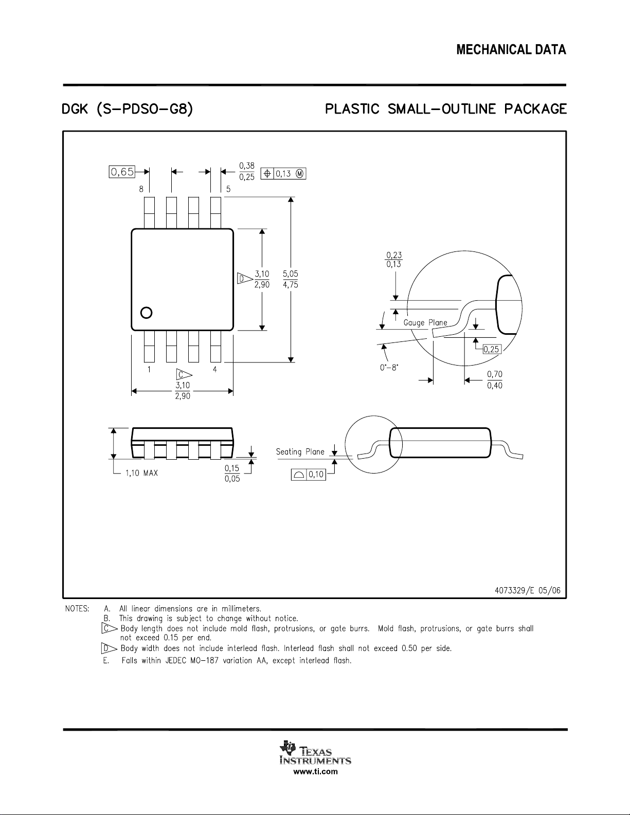
OPA350: P, D, and DGK Packages
8-Pin PDIP, SOIC, and VSSOP
Top View
OPA2350: P, D, and DGK Packages
8-Pin PDIP, SOIC, and VSSOP
Top View
OPA350,OPA2350,OPA4350
SBOS099D –SEPTEMBER 2000–REVISED DECEMBER 2015
D Package
14-Pin SOIC
Top View
DBQ Package
16-Pin SSOP
Top View
Pin Functions
PIN
NAME
OPA350 OPA2350 OPA4350 SO-14 OPA4350 SSOP
NO. NO. NO. NO.
NC 1, 5, 8 — — 8, 9 — No internal connection
–In 2 — — — I Inverting input
+In 3 — — — I Noninverting input
V– 4 4 11 13 I Negative power supply
Output 6 — — — O Output
V+ 7 8 4 4 I Positive power supply
Out A — 1 1 1 O Output channel A
–In A — 2 2 2 I Inverting input channel A
+In A — 3 3 3 I Noninverting input channel A
+In B — 5 5 5 I Noninverting input channel B
–In B — 6 6 6 I Inverting input channel B
Out B — 7 7 7 O Output channel B
Out C — — 8 10 O Output channel C
–In C — — 9 11 I Inverting input channel C
+In C — — 10 12 I Noninverting input channel C
+In D — — 12 14 I Noninverting input channel D
–In D — — 13 15 I Inverting input channel D
Out D — — 14 16 O Output channel D
Copyright © 2000–2015, Texas Instruments Incorporated Submit Documentation Feedback 3
Product Folder Links: OPA350 OPA2350 OPA4350
I/O DESCRIPTION
OPA350,OPA2350,OPA4350
SBOS099D –SEPTEMBER 2000–REVISED DECEMBER 2015
www.ti.com
6 Specifications
6.1 Absolute Maximum Ratings
over operating free-air temperature range (unless otherwise noted)
Supply voltage 7 V
Signal input terminals
(2)
Open short circuit current
(3)
Voltage (V−) − 0.3 (V+) + 0.3 V
Current 10 mA
Operating temperature –55 150 °C
Lead temperature (soldering, 10 s) 300 °C
Junction temperature 150 °C
T
Storage temperature –55 150 °C
stg
(1) Stresses beyond those listed under Absolute Maximum Ratings may cause permanent damage to the device. These are stress ratings
only, which do not imply functional operation of the device at these or any other conditions beyond those indicated under Recommended
Operating Conditions. Exposure to absolute-maximum-rated conditions for extended periods may affect device reliability.
(2) Input terminals are diode-clamped to the power-supply rails. Input signals that can swing more than 0.3 V beyond the supply rails should
be current-limited to 10 mA or less.
(3) Short-circuit to ground, one amplifier per package.
6.2 ESD Ratings
OPA350, OPA2350, OPA4350 (ALL PACKAGE TYPES)
V
(ESD)
OPA350, OPA2350, OPA4350 (SOIC PACKAGES ONLY)
V
(ESD)
(1) JEDEC document JEP155 states that 500-V HBM allows safe manufacturing with a standard ESD control process.
(2) JEDEC document JEP157 states that 250-V CDM allows safe manufacturing with a standard ESD control process.
Electrostatic discharge Human-body model (HBM), per ANSI/ESDA/JEDEC JS-001
Electrostatic discharge ±1500 V
Charged-device model (CDM), per JEDEC specification JESD22-
(2)
C101
(1)
MIN MAX UNIT
Continuous
VALUE UNIT
(1)
±1000 V
6.3 Recommended Operating Conditions
over operating free-air temperature range (unless otherwise noted)
MIN NOM MAX UNIT
Power supply voltage, (V+)-(V-) 2.7 (±1.35) 5 (±2.5) 5.5 (±2.75) V
Specified temperature –40 25 85 °C
Operating temperature –55 25 150 °C
4 Submit Documentation Feedback Copyright © 2000–2015, Texas Instruments Incorporated
Product Folder Links: OPA350 OPA2350 OPA4350
OPA350,OPA2350,OPA4350
www.ti.com
SBOS099D –SEPTEMBER 2000–REVISED DECEMBER 2015
6.4 Thermal Information: OPA350 and OPA2350
OPA350, OPA2350
THERMAL METRIC
(1)
DGK (VSSOP) P (PDIP) D (SOIC) UNIT
8 PINS 8 PINS 8 PINS
R
R
R
ψ
ψ
R
Junction-to-ambient thermal resistance 169.2 53.1 140.1 °C/W
θJA
Junction-to-case (top) thermal resistance 62.8 42.5 89.8 °C/W
θJC(top)
Junction-to-board thermal resistance 89.8 30.3 80.6 °C/W
θJB
Junction-to-top characterization parameter 7.5 19.7 28.7 °C/W
JT
Junction-to-board characterization parameter 88.2 30.2 80.1 °C/W
JB
Junction-to-case (bottom) thermal resistance N/A N/A N/A °C/W
θJC(bot)
(1) For more information about traditional and new thermal metrics, see the IC Package Thermal Metrics application report, SPRA953.
6.5 Thermal Information: OPA4350
OPA4350
THERMAL METRIC
R
θJA
R
θJC(top)
R
θJB
ψ
JT
ψ
JB
R
θJC(bot)
Junction-to-ambient thermal resistance 83.8 115.8 °C/W
Junction-to-case (top) thermal resistance 70.7 67 °C/W
Junction-to-board thermal resistance 59.5 58.3 °C/W
Junction-to-top characterization parameter 11.6 19.9 °C/W
Junction-to-board characterization parameter 37.7 57.9 °C/W
Junction-to-case (bottom) thermal resistance N/A N/A °C/W
(1) For more information about traditional and new thermal metrics, see the Semiconductor and IC Package Thermal Metrics application
report, SPRA953.
(1)
D (SOIC) DBQ (SSOP) UNIT
14 PINS 16 PINS
Copyright © 2000–2015, Texas Instruments Incorporated Submit Documentation Feedback 5
Product Folder Links: OPA350 OPA2350 OPA4350
OPA350,OPA2350,OPA4350
SBOS099D –SEPTEMBER 2000–REVISED DECEMBER 2015
www.ti.com
6.6 Electrical Characteristics
VS= 2.7 V to 5.5 V; All specifications at TA= 25°C, RL= 1 kΩ connected to VS/2 and V
PARAMETER TEST CONDITIONS MIN TYP
OFFSET VOLTAGE
VS= 5 V ±150 ±500 µV
V
PSRR VS= 2.7 V to 5.5 V, VCM= 0 V µV/V
Input offset voltage ±1 mV
OS
vs Power-supply
rejection ratio
Channel separation (dual, quad) DC 0.15 µV/V
INPUT BIAS CURRENT
I
I
Input bias current pA
B
Input offset current ±0.5 ±10 pA
OS
NOISE
Input voltage noise, f = 100 Hz to 400 kHz 4 μVrms
e
Input voltage noise density, f = 10 kHz 7 nV/√Hz
n
Input current noise density, f = 100 kHz 5 nV/√Hz
i
Current noise density, f = 10 kHz 4 fA/√Hz
n
INPUT VOLTAGE RANGE
V
Common-mode voltage range TA= −40°C to 85°C –0.1 (V+) + 0.1 V
CM
CMRR Common-mode rejection ratio dB
INPUT IMPEDANCE
Differential Ω || pF
Common-mode Ω || pF
OPEN-LOOP GAIN
OL
Open-loop voltage
gain
A
FREQUENCY RESPONSE (CL= 100 pF)
GBW Gain-bandwidth product G = 1 38 MHz
SR Slew rate G = 1 22 V/µs
Settling time G = ±1, 2-V Step µs
Overload recovery time VIN× G = V
THD+N Total harmonic distortion + noise RL= 600 Ω, VO= 2.5 V
Differential gain error G = 2, RL= 600 Ω, VO= 1.4 V
Differential phase error G = 2, RL= 600 Ω, VO= 1.4 V
OUTPUT
V
I
I
C
Voltage output swing
OUT
OUT
SC
LOAD
(4)
from rail
Output current ±40
short circuit current ±80 mA
Capacitive load drive See Typical Characteristics
TA= −40°C to
85°C
vs Temperature TA= –40°C to 85°C ±4 μV/°C
vs Temperature See Typical Characteristics
VS= 2.7 V, −0.1 V < VCM< 2.8 V 66 84
VS= 5.5 V, −0.1 V < VCM< 5.6 V 74 90
TA= −40°C to 85°C,
VS= 5.5 V, −0.1 V < VCM< 5.6 V
RL= 10 kΩ, 50 mV < VO< (V+) –50 mV 100 122
RL= 10 kΩ, 50 mV < VO< (V+) –50 mV 100
TA= –40°C to
85°C
RL= 1 kΩ, 200 mV < VO< (V+) –200 mV 100 120
RL= 1 kΩ, 200 mV < VO< (V+) –200 mV 100
0.1% 0.22
0.01% 0.5
S
(2)
, G = 1, f = 1 kHz 0.0006%
PP
(3)
(3)
RL= 10 kΩ, AOL≥ 100 dB 10 50
TA= –40°C to
85°C
RL= 10 kΩ, AOL≥ 100 dB 50 mV
RL= 1 kΩ, AOL≥ 100 dB 25 200
= VS/2, unless otherwise noted.
OUT
(1)
40 150
±0.5 ±10
74
1013|| 2.5
1013|| 6.5
0.1 µs
0.17%
0.17 °
(5)
MAX UNIT
175
dB
mA
(1) VS= 5 V
(2) V
(3) NTSC signal generator used. See Figure 31 for test circuit.
= 0.25 V to 2.75 V
OUT
(4) Output voltage swings are measured between the output and power supply rails.
(5) See Figure 17.
6 Submit Documentation Feedback Copyright © 2000–2015, Texas Instruments Incorporated
Product Folder Links: OPA350 OPA2350 OPA4350
www.ti.com
Electrical Characteristics (continued)
OPA350,OPA2350,OPA4350
SBOS099D –SEPTEMBER 2000–REVISED DECEMBER 2015
VS= 2.7 V to 5.5 V; All specifications at TA= 25°C, RL= 1 kΩ connected to VS/2 and V
PARAMETER TEST CONDITIONS MIN TYP
POWER SUPPLY
V
I
TEMPERATURE RANGE
Operating voltage range TA= −40°C to 85°C 2.7 5.5 V
S
Minimum operating voltage 2.5 V
Quiescent current
Q
(per amplifier)
Specified range –40 85 °C
Operating range –55 150 °C
TA= –40°C to
85°C
IO= 0 mA
= VS/2, unless otherwise noted.
OUT
(1)
5.2 7.5
MAX UNIT
8.5
Copyright © 2000–2015, Texas Instruments Incorporated Submit Documentation Feedback 7
Product Folder Links: OPA350 OPA2350 OPA4350
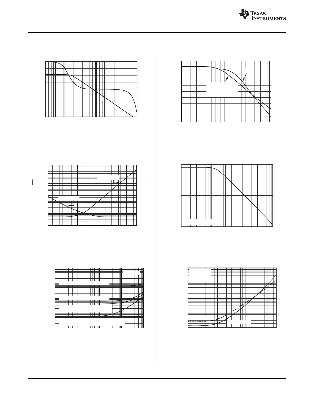
1
0.1
0.01
0.001
0.0001
THD+N (%)
Frequency (Hz)
10 100 1k 10k 100k
RL= 600Ω
G = 100, 3VPP(VO= 1V to 4V)
G = 10, 3VPP(VO= 1V to 4V)
G = 1, 3VPP(VO= 1V to 4V)
Input goes through transition region
G = 1, 2.5VPP(VO= 0.25V to 2.75V)
Input does NOT go through transition region
1
(−40dBc)
0.1
(−60dBc)
0.01
(−80dBc)
0.001
(−100dBc)
0.0001
(−120dBc)
Harmonic Distortion (%)
Frequency (Hz)
1k 10k 100k 1M
G = 1
VO= 2.5V
PP
RL= 600Ω
3rd−Harmonic
2nd−Harmonic
Frequency (Hz)
Channel Separation (dB)
140
130
120
110
100
90
80
70
60
10010 1k 1M100k10k 10M
Dual and quad devices.
100k
10k
1k
100
10
1
10k
1k
100
10
1
0.1
Voltage Noise (nV
√Hz)
Frequency (Hz)
10 100 1k 10k 100k 1M 10M
Current Noise (fA
√
Hz)
Voltage Noise
Current Noise
100
90
80
70
60
50
40
30
20
10
0
PSRR, CMRR (dB)
Frequency (Hz)
10 100 1k 10k 100k 1M 10M
PSRR
CMRR
(V
S
= +5V
V
CM
=−0.1V to 5.1V)
0.1 1
160
140
120
100
80
60
40
20
0
0
−
45
−
90
−
135
−
180
Phase (
)
Frequency (Hz)
10 100 1k 10k 100k 1M 10M 100M
G
φ
Voltage Gain (dB)
OPA350,OPA2350,OPA4350
SBOS099D –SEPTEMBER 2000–REVISED DECEMBER 2015
6.7 Typical Characteristics
All specifications at TA= 25°C, VS= 5 V, and RL= 1 kΩ connected to VS/2, unless otherwise noted.
www.ti.com
Figure 1. Open-Loop Gain and Phase vs Frequency
Figure 3. Input Voltage and Current Noise Spectral Density
vs Frequency
Figure 2. Power Supply and Common-Mode Rejection Ratio
vs Frequency
Figure 4. Channel Separation vs Frequency
Figure 5. Total Harmonic Distortion + Noise vs Frequency
8 Submit Documentation Feedback Copyright © 2000–2015, Texas Instruments Incorporated
Figure 6. Harmonic Distortion + Noise vs Frequency
Product Folder Links: OPA350 OPA2350 OPA4350
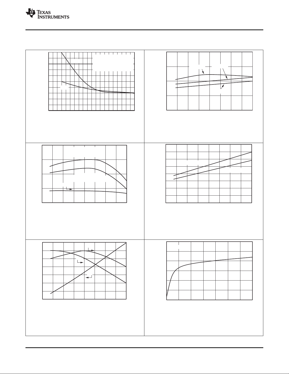
Supply Voltage (V)
Quiescent Current (mA)
6.0
5.5
5.0
4.5
4.0
3.5
3.0
2.0 2.5 3.0 3.5 4.0 4.5 5.0 5.5
Per Amplifier
Temperature ( °C)
Quiescent Current (mA)
7.0
6.5
6.0
5.5
5.0
4.5
4.0
3.5
100
90
80
70
60
50
40
30
Short−Circuit Current (mA)
−75−50−
25 0 25 50 75 100 125
I
Q
+I
SC
−
I
SC
Temperature ( °C)
Slew Rate (V/
µ
s)
40
35
30
25
20
15
10
5
0
−75−50−
25 0 25 50 75 1 00 125
Negative Slew Rate
Positive Slew Rate
100
90
80
70
60
CMRR (dB)
110
100
90
80
70
PSRR (dB)
Temperature ( °C )
−75 −50 −25 0 25 50 75 100 125
CMRR, VS= 5.5V
(VCM=−0.1V to +5.6V)
CMRR, VS= 2.7V
(V
CM
=− 0.1V to +2.8V)
PSRR
0.5
0.4
0.3
0.2
0.1
0
Differential Gain (%)
Differential Phase (°
)
Resistive Load (Ω)
0 100 200 300 500400 600 800700 900 100
0
G = 2
V
O
= 1.4V
NTSC Signal Generator
See Figure 6 for test circuit.
Phase
Gain
130
125
120
115
110
Open−Loop Gain (dB)
Temperature ( °C)
−
75−50−25 0 25 5 0 75 100 125
RL= 600
Ω
RL= 1k
Ω
RL= 10k
Ω
OPA350,OPA2350,OPA4350
www.ti.com
SBOS099D –SEPTEMBER 2000–REVISED DECEMBER 2015
Typical Characteristics (continued)
All specifications at TA= 25°C, VS= 5 V, and RL= 1 kΩ connected to VS/2, unless otherwise noted.
Figure 7. Differential Gain and Phase vs Resistive Load
Figure 9. Common-Mode and Power-Supply Rejection Ratio
vs Temperature
Figure 8. Open-Loop Gain vs Temperature
Figure 10. Slew Rate vs Temperature
Copyright © 2000–2015, Texas Instruments Incorporated Submit Documentation Feedback 9
Figure 11. Quiescent Current and short circuit Current vs
Temperature
Product Folder Links: OPA350 OPA2350 OPA4350
Figure 12. Quiescent Current vs Supply Voltage
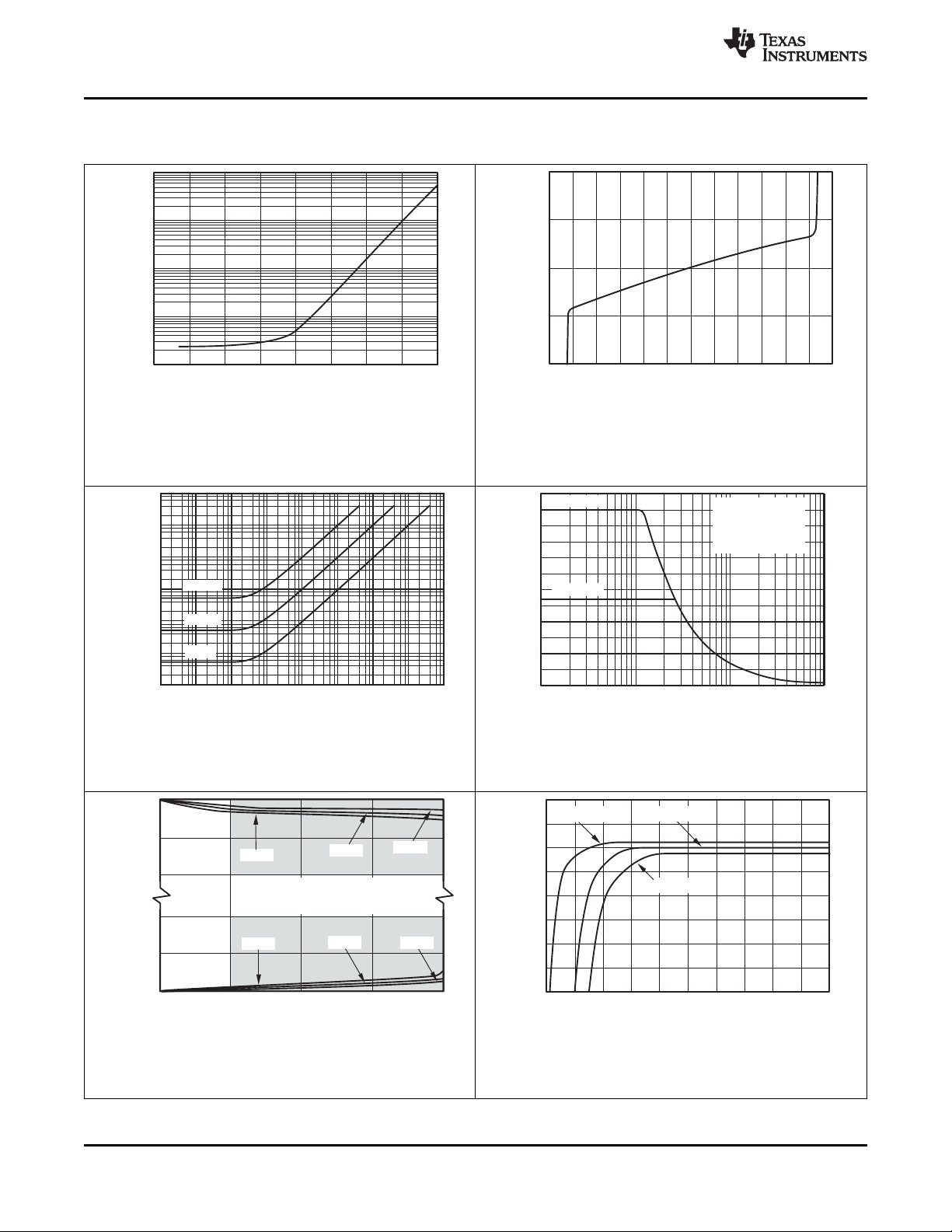
140
130
120
110
100
90
80
70
60
Open−Loop Gain (dB)
Output Voltage Swing from Rails (mV)
0 20 40 6 0 10080 120 160140 180 200
I
OUT
= 4.2mA
I
OUT
= 250µA
I
OUT
= 2.5mA
Output Current (mA)
Output Voltage (V)
V+
(V+)−1
(V+)−2
(V−)+2
(V−)+1
(V−)
0
±
10
±
20
±
30
±
40
+25
°C
+125
°C
−
55
°C
−
55
°C
+125
°C
+25
°C
Depending on circuit configuration
(including closed−loop gain) performance
may be degraded in shaded region.
100M1M 10M
Frequency (Hz)
100k
6
5
4
3
2
1
0
Output Voltage (V
PP
)
Maximum output
voltage without
slew rate−induced
distortion.
VS= 2.7V
VS= 5.5V
Frequency (Hz)
Output Impedance (
Ω
)
100
10
1
0.1
0.01
0.001
0.0001
1 10 100 1k 10k 100k 1M 10M 100
M
G = 100
G = 10
G = 1
Common−Mode Voltage (V)
Input Bias Current (pA)
1.5
1.0
0.5
0.0
−
0.5
−0.5 0.0 0.5 1.0 2.01.5 2.5 3.0 3.5 4.0 5.04.5 5.5
Input Bias Current (pA)
Temperature (
°C)
−75−50−
25 0 25 50 75 100 125
1k
100
10
1
0.1
OPA350,OPA2350,OPA4350
SBOS099D –SEPTEMBER 2000–REVISED DECEMBER 2015
Typical Characteristics (continued)
All specifications at TA= 25°C, VS= 5 V, and RL= 1 kΩ connected to VS/2, unless otherwise noted.
www.ti.com
Figure 13. Input Bias Current vs Temperature
Figure 15. Closed-Loop Output Impedance vs Frequency
Figure 14. Input Bias Current vs Input Common-Mode
Voltage
Figure 16. Maximum Output Voltage vs Frequency
10 Submit Documentation Feedback Copyright © 2000–2015, Texas Instruments Incorporated
Figure 17. Output Voltage Swing vs Output Current
Figure 18. Open-Loop Gain vs Output Voltage Swing
Product Folder Links: OPA350 OPA2350 OPA4350

100ns/div
50mV/div
200ns/div
1V/div
10
1
0.1
Settling Time (
µ
s)
Closed−Loop Gain (V/V)
−
1
−
10
−
100
0.1%
0.01%
1M100 1k 10k 100k
Load Capacitance (pF)
10
80
70
60
50
40
30
20
10
0
Overshoot (%)
G = 1
G=−1
G =±10
Offset Voltage Drift (µV/
°C)
20
18
16
14
12
10
8
6
4
2
0
0 1 2 3 4 5 6 7 8 9 10 11 12 13 14 15
Percent of Amplifiers (%)
Typical production
distribution of
packaged units.
Offset Voltage (µV)
18
16
14
12
10
8
6
4
2
0
Percent of Amplifiers (%)
−
500
−
450
−
400
−
350
−
300
−
250
−
200
−
150
−
100
−
50
0
50
100
150
200
250
300
350
400
450
500
Typical distribution of
packaged units.
OPA350,OPA2350,OPA4350
www.ti.com
SBOS099D –SEPTEMBER 2000–REVISED DECEMBER 2015
Typical Characteristics (continued)
All specifications at TA= 25°C, VS= 5 V, and RL= 1 kΩ connected to VS/2, unless otherwise noted.
Figure 19. Offset Voltage Production Distribution
Figure 21. Small-Signal Overshoot vs Load Capacitance
Figure 20. Offset Voltage Drift Production Distribution
Figure 22. Settling Time vs Closed-Loop Gain
Copyright © 2000–2015, Texas Instruments Incorporated Submit Documentation Feedback 11
Figure 23. Small-Signal Step Response Figure 24. Large-Signal Step Response
CL= 100 pF CL= 100 pF
Product Folder Links: OPA350 OPA2350 OPA4350
Reference
Current
V+
V
IN-
V
IN+
V
(Ground)
-
V
BIAS2
V
BIAS1
Class AB
Control
Circuitry
V
O
OPA350,OPA2350,OPA4350
SBOS099D –SEPTEMBER 2000–REVISED DECEMBER 2015
www.ti.com
7 Detailed Description
7.1 Overview
The OPA350 series rail-to-rail CMOS operational amplifiers are optimized for low voltage, single-supply
operation. Rail-to-rail input and output, low noise (5 nV/√Hz), and high speed operation (38 MHz, 22 V/μs) make
the amplifiers ideal for driving sampling Analog-to-Digital (A/D) converters. They are also suited for cell phone PA
control loops and video processing (75-Ω drive capability), as well as audio and general purpose applications.
Single, dual, and quad versions have identical specifications for maximum design flexibility.
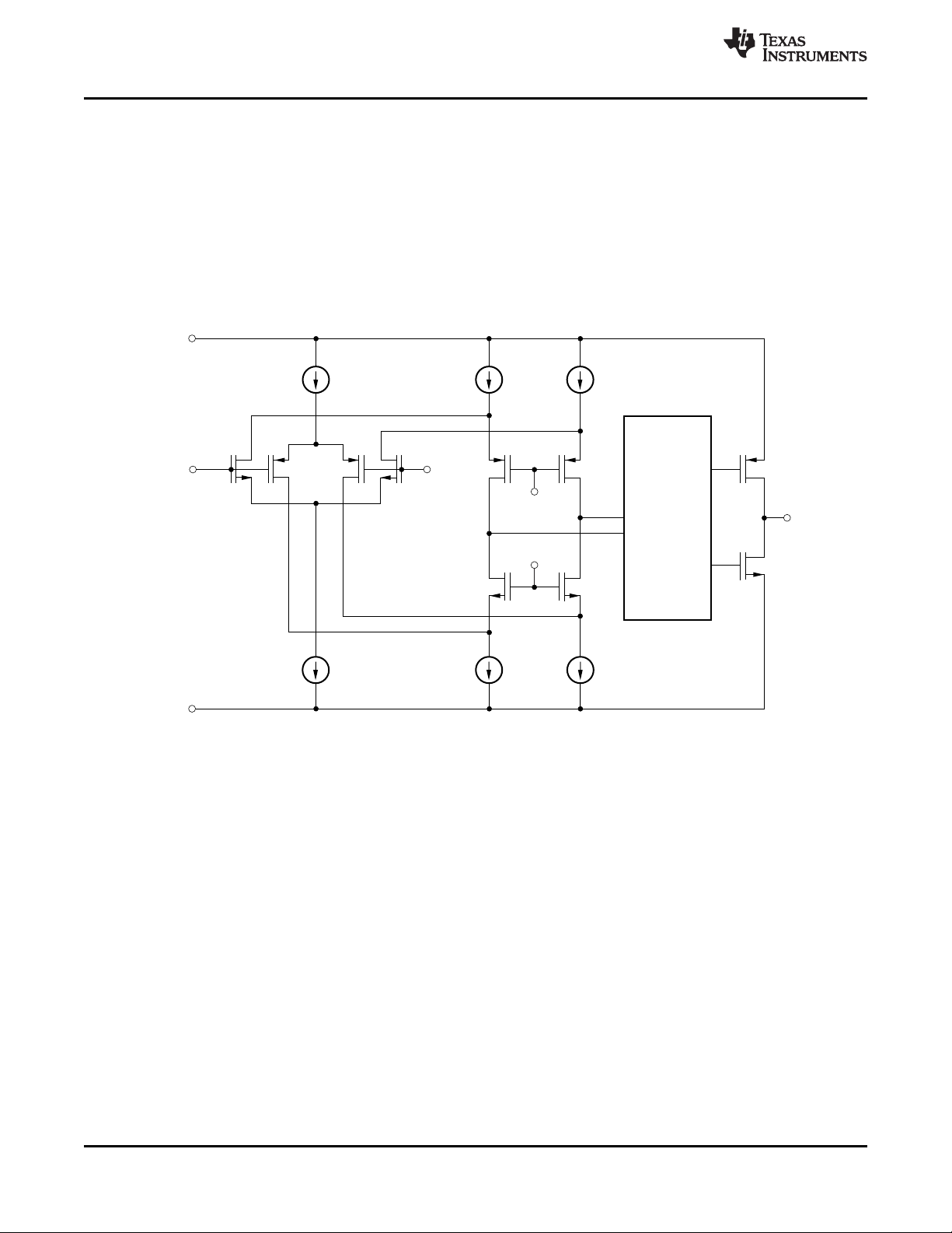
7.2 Functional Block Diagram
7.3 Feature Description
The OPA350 series of operational amplifiers (op amps) are fabricated on a state-of-the-art 0.6 micron CMOS
process. They are unity-gain stable and suitable for a wide range of general purpose applications. Rail-to-rail
input and output make them ideal for driving sampling A/D converters. They are also suited for controlling the
output power in cell phones. These applications often require high speed and low noise. In addition, the OPA350
series offers a low-cost solution for general-purpose and consumer video applications (75-Ω drive capability).
Excellent AC performance makes the OPA350 series suited for audio applications. Their bandwidth, slew rate,
low noise (5 nV/√Hz), low THD (0.0006%), and small package options are ideal for these applications. The class
AB output stage is capable of driving 600-Ω loads connected to any point between V+ and ground.
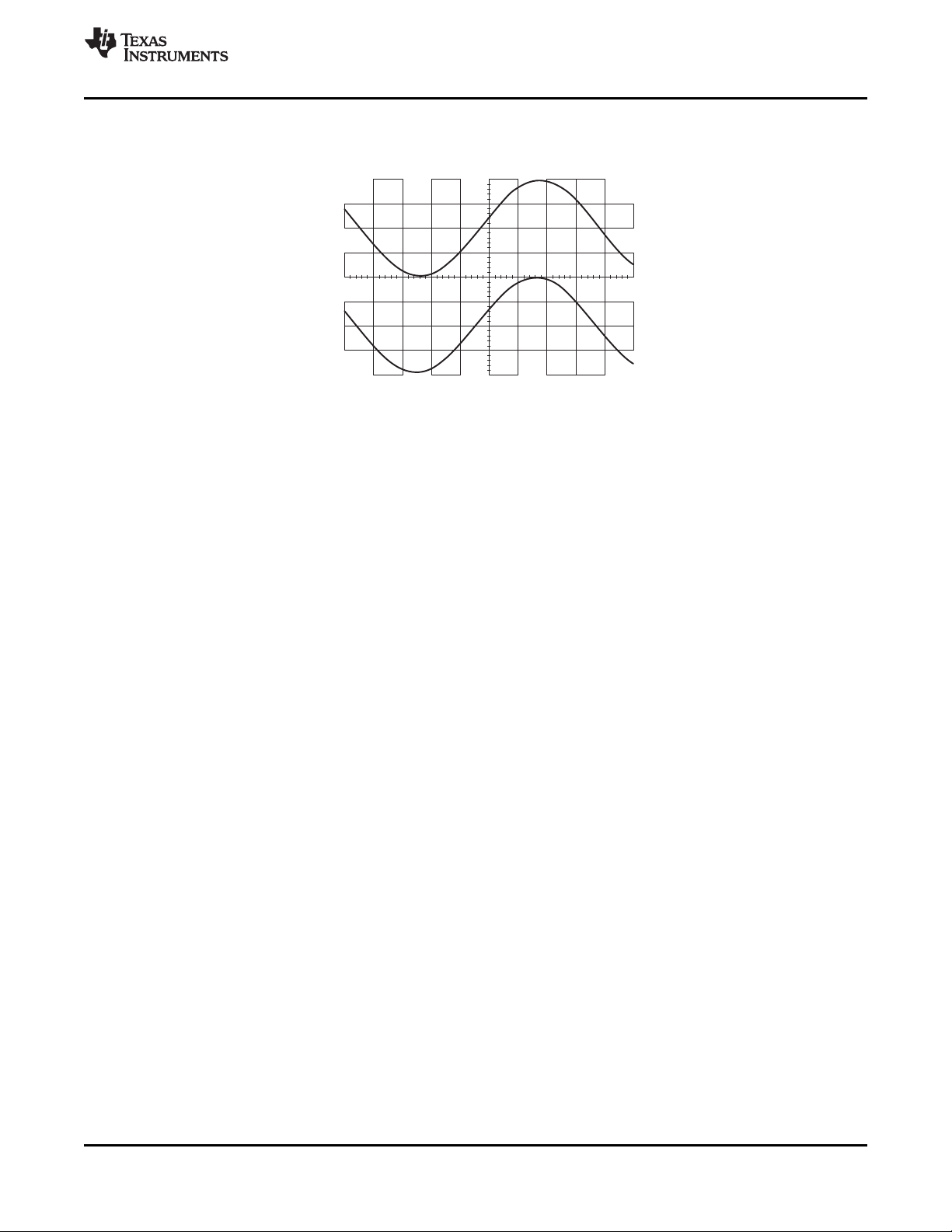
Rail-to-rail input and output swing significantly increases dynamic range, especially in low voltage supply
applications. Figure 25 shows the input and output waveforms for the OPA350 in unity-gain configuration.
Operation is from a single 5-V supply with a 1-kΩ load connected to VS/2. The input is a 5 VPPsinusoid. Output
voltage swing is approximately 4.95 VPP.
Power supply pins should be bypassed with 0.01-μF ceramic capacitors.
12 Submit Documentation Feedback Copyright © 2000–2015, Texas Instruments Incorporated
Product Folder Links: OPA350 OPA2350 OPA4350
VS= +5, G = +1, RL= 1k
Ω
5V
V
IN
0
5V
V
OUT
0
1.25V/div
OPA350,OPA2350,OPA4350
www.ti.com
SBOS099D –SEPTEMBER 2000–REVISED DECEMBER 2015
Feature Description (continued)
Figure 25. Rail-to-Rail Input and Output
7.3.1 Operating Voltage
OPA350 series operational amplifiers are fully specified from 2.7 V to 5.5 V. Supply voltage may range from 2.5
V to 5.5 V. Parameters are tested over the specified supply range: a feature of the OPA350 series. In addition,
many specifications apply from −40°C to 85°C. Most behavior remains virtually unchanged throughout the full
operating voltage range. Parameters that vary significantly with operating voltage or temperature are shown in
Typical Characteristics.
7.3.2 Rail-to-Rail Input
The tested input common-mode voltage range of the OPA350 series extends 100 mV beyond the supply rails.
This is achieved with a complementary input stage: an N-channel input-differential pair in parallel with a Pchannel differential pair, as shown in Figure 26. The N-channel pair is active for input voltages close to the
positive rail, typically (V+) – 1.8 V to 100 mV above the positive supply, while the P-channel pair is on for inputs
from 100 mV below the negative supply to approximately (V+) – 1.8 V. There is a small transition region, typically
(V+) – 2 V to (V+) – 1.6 V, in which both pairs are on. This 400-mV transition region can vary ±400 mV with
process variation. Thus, the transition region (both input stages on) can range from (V+) – 2.4 V to (V+) – 2 V on
the low end, up to (V+) – 1.6 V to (V+) – 1.2 V on the high end.
Copyright © 2000–2015, Texas Instruments Incorporated Submit Documentation Feedback 13
Product Folder Links: OPA350 OPA2350 OPA4350

5k
Ω
OPA x350
10mA max
V+
V
IN
V
OUT
I
OVERLOAD
V
BIAS1
V
BIAS2
VIN+
V
IN
−
Class AB
Control
Circuitry
V
O
V
−
(Ground)
V+
Reference
Current
OPA350,OPA2350,OPA4350
SBOS099D –SEPTEMBER 2000–REVISED DECEMBER 2015
Feature Description (continued)
www.ti.com
Figure 26. Simplified Schematic
OPA350 series operational amplifiers are laser-trimmed to reduce offset voltage difference between the Nchannel and P-channel input stages, resulting in improved common-mode rejection and a smooth transition
between the N-channel pair and the P-channel pair. However, within the 400-mV transition region PSRR, CMRR,
offset voltage, offset drift, and THD may be degraded compared to operation outside this region.
A double-folded cascode adds the signal from the two input pairs and presents a differential signal to the class
AB output stage. Normally, input bias current is approximately 500 fA. However, large inputs (greater than 300
mV beyond the supply rails) can turn on the input protection diodes, causing excessive current to flow in or out of
the input pins. Momentary voltages greater than 300 mV beyond the power supply can be tolerated if the current
on the input pins is limited to 10 mA. This is easily accomplished with an input resistor, as shown in Figure 27.
Many input signals are inherently current-limited to less than 10 mA; therefore, a limiting resistor is not required.
Figure 27. Input Current Protection for Voltages Exceeding the Supply Voltage
7.3.3 Rail-to-Rail Output
A class AB output stage with common-source transistors achieves rail-to-rail output. For light resistive loads (>10
kΩ), the output voltage swing is typically ten millivolts from the supply rails. With heavier resistive loads (600 Ω to
10 kΩ), the output can swing to within a few tens of millivolts from the supply rails and maintain high open-loop
gain. See Figure 17 and Figure 18 for more information.
14 Submit Documentation Feedback Copyright © 2000–2015, Texas Instruments Incorporated
Product Folder Links: OPA350 OPA2350 OPA4350

OPA350,OPA2350,OPA4350
www.ti.com
SBOS099D –SEPTEMBER 2000–REVISED DECEMBER 2015
Feature Description (continued)
7.3.4 Capacitive Load and Stability
OPA350 series operational amplifiers can drive a wide range of capacitive loads. However, all operational
amplifiers under certain conditions may become unstable. operational amplifier configuration, gain, and load
value are just a few of the factors to consider when determining stability. An operational amplifier in unity-gain
configuration is the most susceptible to the effects of capacitive load. The capacitive load reacts with the output
impedance of the operational amplifier, along with any additional load resistance, to create a pole in the smallsignal response that degrades the phase margin.
In unity gain, OPA350 series operational amplifiers perform well with large capacitive loads. Increasing gain
enhances the ability of the amplifier to drive more capacitance. Figure 21 shows performance with a 1-kΩ
resistive load. Increasing load resistance improves capacitive load drive capability.
7.3.5 Driving A/D Converters
OPA350 series operational amplifiers are optimized for driving medium speed (up to 500 kHz) sampling A/D
converters, and also offer excellent performance for higher speed converters. The OPA350 series provides an
effective means of buffering the input capacitance of the A/D and resulting charge injection while providing signal
gain.
Figure 28 shows the OPA350 driving an ADS7861. The ADS7861 is a dual, 500 kHz, 12-bit sampling converter
in the tiny SSOP-24 package. When used with the miniature package options of the OPA350 series, the
combination is ideal for space-limited applications. For further information, consult the ADS7861 data sheet,
Dual, 500kSPS, 12-Bit, 2 + 2 Channel, Simultaneous Sampling ANALOG-TO-DIGITAL CONVERTER
(SBAS110).
Copyright © 2000–2015, Texas Instruments Incorporated Submit Documentation Feedback 15
Product Folder Links: OPA350 OPA2350 OPA4350

1/ 4
O PA 435 0
VINB1
2
3
4
2k
Ω
2k
Ω
C
B1
CH B1+
CH B1
−
CH B0+
CH B0
−
CH A1+
CH A1
−
CH A0+
CH A0
−
REF
IN
REF
OUT
SERIAL DATA A
SERIAL DATA B
BUSY
CLOCK
CS
RD
CONVST
A0
M0
M1
2
3
4
5
6
7
8
9
10
11
23
22
21
20
19
18
17
16
15
14
1/ 4
O PA 435 0
VINB0
+5V
6
5
2k
Ω
2k
Ω
C
B0
1/ 4
O PA 435 0
VINA1
9
10
12
13
8
7
1
2k
Ω
2k
Ω
C
A1
1/ 4
O PA 435 0
VINA0
14
11
1 12
2k
Ω
2k
Ω
C
A0
0.1µF 0.1µF
+V
A
+V
D
24 13
Serial
Interface
DGND AGND
ADS7861
VIN= 0V to 2.45V for 0V to 4.9V output.
Choose C
B1
, CB0, CA1, CA0to filter high frequency noise.
OPA350,OPA2350,OPA4350
SBOS099D –SEPTEMBER 2000–REVISED DECEMBER 2015
Feature Description (continued)
www.ti.com
Figure 28. OPA4350 Driving Sampling A/D Converter
7.3.6 Output Impedance
The low-frequency open-loop output impedance of the common-source output stage of the OPA350 is
approximately 1 kΩ. When the operational amplifier is connected with feedback, this value is reduced
significantly by the loop gain of the operational amplifier. For example, with 122 dB of open-loop gain, the output
impedance is reduced in unity-gain to less than 0.001 Ω. For each decade rise in the closed-loop gain, the loop
gain is reduced by the same amount which results in a ten-fold increase in effective output impedance (see
Figure 15).
At higher frequencies, the output impedance rises as the open-loop gain of the operational amplifier drops.
However, at these frequencies the output also becomes capacitive due to parasitic capacitance. This prevents
the output impedance from becoming too high, which can cause stability problems when driving capacitive loads.
The OPA350 has excellent capacitive load drive capability for an operational amplifier with its bandwidth.
16 Submit Documentation Feedback Copyright © 2000–2015, Texas Instruments Incorporated
Product Folder Links: OPA350 OPA2350 OPA4350

OPA350,OPA2350,OPA4350
www.ti.com
SBOS099D –SEPTEMBER 2000–REVISED DECEMBER 2015
7.4 Device Functional Modes
The OPAx350 has a single functional mode and is operational when the power-supply voltage is greater than
2.7 V (±1.35 V). The maximum power supply voltage for the OPAx350 is 5.5V (±2.75 V).
Copyright © 2000–2015, Texas Instruments Incorporated Submit Documentation Feedback 17
Product Folder Links: OPA350 OPA2350 OPA4350

4
1
C 3 4 2 5
R
Gain
R
1
f 1 R R C C
2
S
1 3 2 5
2
2 1 3 4 3 4 2 5
1R R C C
Output
s
Input
s s C 1 R 1R 1 R 1R R C C
+
±
OPAx350
Output
Input
R1
590
R4
2.94 k
R3
499
C2
39 nF
C5
1 nF
OPA350,OPA2350,OPA4350
SBOS099D –SEPTEMBER 2000–REVISED DECEMBER 2015
www.ti.com
8 Application and Implementation
NOTE
Information in the following applications sections is not part of the TI component
specification, and TI does not warrant its accuracy or completeness. TI’s customers are
responsible for determining suitability of components for their purposes. Customers should
validate and test their design implementation to confirm system functionality.
8.1 Application Information
Low pass filters are commonly employed in signal processing applications to reduce noise and prevent aliasing.
The OPAx350 are ideally suited to construct high speed, high precision active filters. Figure 29 illustrates a
second order low pass filter commonly encountered in signal processing applications.
8.2 Typical Applications
8.2.1 Second Order Low Pass Filter
8.2.1.1 Design Requirements
Use the following parameters for this design example:
• Gain = 5 V/V (inverting gain).
• Low pass cutoff frequency = 25 kHz.
• Second order Chebyshev filter response with 3-dB gain peaking in the passband.
8.2.1.2 Detailed Design Procedure
The infinite-gain multiple-feedback circuit for a low-pass network function is shown in Equation 1. Use Equation 2
to calculate the voltage transfer function.
This circuit produces a signal inversion. For this circuit the gain at DC and the low pass cutoff frequency can be
calculated using Equation 2.
Software tools are readily available to simplify filter design. WEBENCH® Filter Designer is a simple, powerful,
and easy-to-use active filter design program. The WEBENCH Filter Designer lets you create optimized filter
designs using a selection of TI operational amplifiers and passive components from TI's vendor partners.
Available as a web based tool from the WEBENCH® Design Center, WEBENCH® Filter Designer allows you to
design, optimize, and simulate complete multi-stage active filter solutions within minutes.
18 Submit Documentation Feedback Copyright © 2000–2015, Texas Instruments Incorporated
Figure 29. Second Order Low Pass Filter
Product Folder Links: OPA350 OPA2350 OPA4350
(1)
(2)

OPA350
+5V
V
OUT
+5V (pin 7)
Video
In
R
OUT
R
L
Cable
R
F
1k
Ω
R
G
1k
Ω
R
4
5k
Ω
R
3
5k
Ω
C
3
10µF
0.1µF 10µF
+
6
7
4
3
2
C
4
0.1µF
C
5
1000µF
C
2
47µF
R
2
5k
Ω
R
1
75
Ω
C
1
220µF
Frequency (Hz)
Gain (db)
-60
-40
-20
0
20
100 1k 10k 100k 1M
OPA350,OPA2350,OPA4350
www.ti.com
SBOS099D –SEPTEMBER 2000–REVISED DECEMBER 2015
Typical Applications (continued)
8.2.1.3 Application Curve
Figure 30. OPAx350 2nd Order 25-kHz, Chebyshev, Low-Pass Filter
8.2.2 Single-Supply Video Line Driver
Figure 31 shows a circuit for a single supply, G = 2 composite video line driver. The synchronized outputs of a
composite video line driver extend below ground. As shown, the input to the operational amplifier should be ACcoupled and shifted positively to provide adequate signal swing to account for these negative signals in a singlesupply configuration.
The input is terminated with a 75-Ω resistor and AC-coupled with a 47-μF capacitor to a voltage divider that
provides the DC bias point to the input. In Figure 31, this point is approximately (V−) + 1.7 V. Setting the optimal
bias point requires some understanding of the nature of composite video signals. For best performance, avoid
the distortion caused by the transition region of the complementary input stage of the OPA350. See the
discussion of rail-to-rail input in Rail-to-Rail Input.
Copyright © 2000–2015, Texas Instruments Incorporated Submit Documentation Feedback 19
Figure 31. Single-Supply Video Line Driver
Product Folder Links: OPA350 OPA2350 OPA4350

O PA 35 0
V+
V
OUT
V
IN
R
IN
R
IN
•
C
IN
= R
F
•
C
F
R
C
F
L
C
IN
C
IN
C
F
Where CINis equal to the OPA350’s input
capacitance (approximately 9pF) plus any
parasitic layout capacitance.
OPA350,OPA2350,OPA4350
SBOS099D –SEPTEMBER 2000–REVISED DECEMBER 2015
www.ti.com
Typical Applications (continued)
8.2.3 Adding a Feedback Capacitor to Improve Response
For optimum settling time and stability with high-impedance feedback networks, it may be necessary to add a
feedback capacitor across the feedback resistor, RF, as shown in Figure 32. This capacitor compensates for the
zero created by the feedback network impedance and the input capacitance of the OPA350 (and any parasitic
layout capacitance). The effect becomes more significant with higher impedance networks.
Figure 32. Feedback Capacitor Improves Dynamic Performance
A variable capacitor can be used for the feedback capacitor, because input capacitance may vary between
operational amplifiers and layout capacitance is difficult to determine. For the circuit shown in Figure 32, the
value of the variable feedback capacitor should be chosen so that the input resistance times the input
capacitance of the OPA350 (typically 9 pF) plus the estimated parasitic layout capacitance equals the feedback
capacitor times the feedback resistor:
RIN× CIN= RF× C
F
where
• CINis equal to the input capacitance of the OPA350 (sum of differential and common-mode) plus the layout
capacitance. (3)
The capacitor can be varied until optimum performance is obtained.
8.2.4 Two Op-Amp Instrumentation Amplifier With Improved High-Frequency Common-Mode Rejection
The OPAx350 is well suited for high input impedance applications such as an instrumentation amplifier. The two
amplifier configuration shown in Figure 33 rejects any common mode signals and senses the small differential
input voltage developed by the resistive bridge. The voltage reference sets the output to 2.5 V when the
differential signal developed by the bridge is zero. The high common mode rejection versus frequency response
of the OPAx350, rejects and common mode noise that may be coupled into the bridge circuit from the bridge
excitation source. The gain of the circuit is determined by RGaccording to the equation shown in Figure 33.
20 Submit Documentation Feedback Copyright © 2000–2015, Texas Instruments Incorporated
Product Folder Links: OPA350 OPA2350 OPA4350

+2.5V
V
IN
C
2
270pF
C
1
1830pF
−2.5V
R
2
49.9k
Ω
R
L
20kΩ
OPA350
V
OUT
R
1
10.5k
Ω
1/ 2
O PA 235 0
1/ 2
O PA 235 0
R
3
25k
Ω
R
2
25k
Ω
R
R
G
1
100k
Ω
R
4
100k
Ω
R
L
10k
Ω
V
O
50k
Ω
G = 5 +
200k
Ω
R
G
+5V
+5V
REF1004−2.5
4
8
(2.5V)
www.ti.com
Typical Applications (continued)
OPA350,OPA2350,OPA4350
SBOS099D –SEPTEMBER 2000–REVISED DECEMBER 2015
8.2.5 10-kHz High-Pass Filter
High-pass filters are used to reject DC signals and low-frequency time varying signals such as drift versus
temperature. Figure 34 illustrates a high-pass filter with a 10 kHz low-frequency cutoff frequency.
Figure 33. Two Op-Amp Instrumentation Amplifier With Improved High-Frequency Common-Mode
Rejection Schematic
Figure 34. 10-kHz High-Pass Filter
Copyright © 2000–2015, Texas Instruments Incorporated Submit Documentation Feedback 21
Product Folder Links: OPA350 OPA2350 OPA4350

OPA350,OPA2350,OPA4350
SBOS099D –SEPTEMBER 2000–REVISED DECEMBER 2015
www.ti.com
9 Power Supply Recommendations
The OPAx350 are specified for operation from 2.7 V to 5.5 V (±1.35 V to ±2.75 V); many specifications apply
from –40°C to 85°C. Parameters that can exhibit significant variance with regard to operating voltage or
temperature are presented in the Typical Characteristics.
10 Layout
10.1 Layout Guidelines
For best operational performance of the device, use good PCB layout practices, including:
• Noise can propagate into analog circuitry through the power pins of the circuit as a whole and operational
amplifier itself. Bypass capacitors are used to reduce the coupled noise by providing low-impedance
power sources local to the analog circuitry.
– Connect low-ESR, 0.1-µF ceramic bypass capacitors between each supply pin and ground, placed as
close to the device as possible. A single bypass capacitor from V+ to ground is applicable for singlesupply applications.
• Separate grounding for analog and digital portions of circuitry is one of the simplest and most-effective
methods of noise suppression. One or more layers on multilayer PCBs are usually devoted to ground
planes. A ground plane helps distribute heat and reduces EMI noise pickup. Make sure to physically
separate digital and analog grounds paying attention to the flow of the ground current. For more detailed
information, see Circuit Board Layout Techniques (SLOA089).
• To reduce parasitic coupling, run the input traces as far away from the supply or output traces as
possible. If these traces cannot be kept separate, crossing the sensitive trace perpendicular is much
better as opposed to in parallel with the noisy trace.
• Place the external components as close to the device as possible. As illustrated in Figure 35, keeping RF
and RG close to the inverting input minimizes parasitic capacitance.
• Keep the length of input traces as short as possible. Always remember that the input traces are the most
sensitive part of the circuit.
• Consider a driven, low-impedance guard ring around the critical traces. A guard ring can significantly
reduce leakage currents from nearby traces that are at different potentials.
• Cleaning the PCB following board assembly is recommended for best performance.
• Any precision integrated circuit may experience performance shifts due to moisture ingress into the
plastic package. Following any aqueous PCB cleaning process, baking the PCB assembly is
recommended to remove moisture introduced into the device packaging during the cleaning process. A
low temperature, post cleaning bake at 85°C for 30 minutes is sufficient for most circumstances.
22 Submit Documentation Feedback Copyright © 2000–2015, Texas Instruments Incorporated
Product Folder Links: OPA350 OPA2350 OPA4350

N/C
±IN
+IN
V±
V+
OUTPUT
N/C
N/C
VS+
GND
VS±
GND
Ground (GND) plane on another layer
VOUT
VIN
GND
Run the input traces
as far away from
the supply lines
as possible
Use low-ESR, ceramic
bypass capacitor
RF
RG
Place components
close to device and to
each other to reduce
parasitic errors
+
VIN
VOUT
RG
RF
(Schematic Representation)
Use low-ESR,
ceramic bypass
capacitor
www.ti.com
10.2 Layout Example
OPA350,OPA2350,OPA4350
SBOS099D –SEPTEMBER 2000–REVISED DECEMBER 2015
Figure 35. Operational Amplifier Board Layout for Noninverting Configuration
Copyright © 2000–2015, Texas Instruments Incorporated Submit Documentation Feedback 23
Product Folder Links: OPA350 OPA2350 OPA4350

OPA350,OPA2350,OPA4350
SBOS099D –SEPTEMBER 2000–REVISED DECEMBER 2015
www.ti.com
11 Device and Documentation Support
11.1 Device Support
11.1.1 Development Support
11.1.1.1 TINA-TI™ (Free Software Download)
TINA™ is a simple, powerful, and easy-to-use circuit simulation program based on a SPICE engine. TINA-TI™ is
a free, fully-functional version of the TINA software, preloaded with a library of macro models in addition to a
range of both passive and active models. TINA-TI provides all the conventional DC, transient, and frequency
domain analysis of SPICE, as well as additional design capabilities.
Available as a free download from the Analog eLab Design Center, TINA-TI offers extensive post-processing
capability that allows users to format results in a variety of ways. Virtual instruments offer the ability to select
input waveforms and probe circuit nodes, voltages, and waveforms, creating a dynamic quick-start tool.
WEBENCH® Filter Designer is a simple, powerful, and easy-to-use active filter design program. The WEBENCH
Filter Designer lets you create optimized filter designs using a selection of TI operational amplifiers and passive
components from TI's vendor partners. Available as a web based tool from the WEBENCH® Design Center,
WEBENCH® Filter Designer allows you to design, optimize, and simulate complete multi-stage active filter
solutions within minutes.
NOTE
These files require that either the TINA software (from DesignSoft™) or TINA-TI software
be installed. Download the free TINA-TI software from the TINA-TI folder.
11.1.1.2 TI Precision Designs
The OPA350 is featured in several TI Precision Designs, available online at
http://www.ti.com/ww/en/analog/precision-designs/. TI Precision Designs are analog solutions created by TI’s
precision analog applications experts and offer the theory of operation, component selection, simulation,
complete PCB schematic and layout, bill of materials, and measured performance of many useful circuits.
11.2 Documentation Support
11.2.1 Related Documentation
For related documentation see the following:
• Circuit Board Layout Techniques, SLOA089
• Op Amps for Everyone, SLOD006
• Compensate Transimpedance Amplifiers Intuitively, SBOS055
• Noise Analysis for High Speed op Amps, SBOA066
11.3 Related Links
The table below lists quick access links. Categories include technical documents, support and community
resources, tools and software, and quick access to sample or buy.
Table 1. Related Links
PARTS PRODUCT FOLDER SAMPLE & BUY
OPA350 Click here Click here Click here Click here Click here
OPA2350 Click here Click here Click here Click here Click here
OPA4350 Click here Click here Click here Click here Click here
TECHNICAL TOOLS & SUPPORT &
DOCUMENTS SOFTWARE COMMUNITY
24 Submit Documentation Feedback Copyright © 2000–2015, Texas Instruments Incorporated
Product Folder Links: OPA350 OPA2350 OPA4350

OPA350,OPA2350,OPA4350
www.ti.com
SBOS099D –SEPTEMBER 2000–REVISED DECEMBER 2015
11.4 Community Resources
The following links connect to TI community resources. Linked contents are provided "AS IS" by the respective
contributors. They do not constitute TI specifications and do not necessarily reflect TI's views; see TI's Terms of
Use.
TI E2E™ Online Community TI's Engineer-to-Engineer (E2E) Community. Created to foster collaboration
among engineers. At e2e.ti.com, you can ask questions, share knowledge, explore ideas and help
solve problems with fellow engineers.
Design Support TI's Design Support Quickly find helpful E2E forums along with design support tools and
contact information for technical support.
11.5 Trademarks
TINA-TI, E2E are trademarks of Texas Instruments.
TINA, DesignSoft are trademarks of DesignSoft, Inc.
All other trademarks are the property of their respective owners.
11.6 Electrostatic Discharge Caution
These devices have limited built-in ESD protection. The leads should be shorted together or the device placed in conductive foam
during storage or handling to prevent electrostatic damage to the MOS gates.
11.7 Glossary
SLYZ022 — TI Glossary.
This glossary lists and explains terms, acronyms, and definitions.
12 Mechanical, Packaging, and Orderable Information
The following pages include mechanical, packaging, and orderable information. This information is the most
current data available for the designated devices. This data is subject to change without notice and revision of
this document. For browser-based versions of this data sheet, refer to the left-hand navigation.
Copyright © 2000–2015, Texas Instruments Incorporated Submit Documentation Feedback 25
Product Folder Links: OPA350 OPA2350 OPA4350

PACKAGE OPTION ADDENDUM
www.ti.com
PACKAGING INFORMATION
Orderable Device Status
OPA2350EA/250 ACTIVE VSSOP DGK 8 250 Green (RoHS
OPA2350EA/250G4 ACTIVE VSSOP DGK 8 250 Green (RoHS
OPA2350EA/2K5 ACTIVE VSSOP DGK 8 2500 Green (RoHS
OPA2350EA/2K5G4 ACTIVE VSSOP DGK 8 2500 Green (RoHS
OPA2350PA LIFEBUY PDIP P 8 50 Green (RoHS
OPA2350PAG4 LIFEBUY PDIP P 8 50 Green (RoHS
OPA2350UA ACTIVE SOIC D 8 75 Green (RoHS
OPA2350UA/2K5 ACTIVE SOIC D 8 2500 Green (RoHS
OPA2350UA/2K5G4 ACTIVE SOIC D 8 2500 Green (RoHS
OPA2350UAG4 ACTIVE SOIC D 8 75 Green (RoHS
OPA350EA/250 ACTIVE VSSOP DGK 8 250 Green (RoHS
OPA350EA/250G4 ACTIVE VSSOP DGK 8 250 Green (RoHS
OPA350EA/2K5 ACTIVE VSSOP DGK 8 2500 Green (RoHS
OPA350EA/2K5G4 ACTIVE VSSOP DGK 8 2500 Green (RoHS
OPA350PA ACTIVE PDIP P 8 50 Green (RoHS
OPA350PAG4 ACTIVE PDIP P 8 50 Green (RoHS
OPA350UA ACTIVE SOIC D 8 75 Green (RoHS
Package Type Package
(1)
Drawing
Pins Package
Qty
Eco Plan
(2)
& no Sb/Br)
& no Sb/Br)
& no Sb/Br)
& no Sb/Br)
& no Sb/Br)
& no Sb/Br)
& no Sb/Br)
& no Sb/Br)
& no Sb/Br)
& no Sb/Br)
& no Sb/Br)
& no Sb/Br)
& no Sb/Br)
& no Sb/Br)
& no Sb/Br)
& no Sb/Br)
& no Sb/Br)
Lead/Ball Finish
(6)
MSL Peak Temp
(3)
Op Temp (°C) Device Marking
CU NIPDAUAG Level-2-260C-1 YEAR -40 to 85 D50
CU NIPDAUAG Level-2-260C-1 YEAR -40 to 85 D50
CU NIPDAUAG Level-2-260C-1 YEAR -40 to 85 D50
CU NIPDAUAG Level-2-260C-1 YEAR -40 to 85 D50
CU NIPDAU N / A for Pkg Type -40 to 85 OPA2350PA
CU NIPDAU N / A for Pkg Type -40 to 85 OPA2350PA
CU NIPDAU Level-2-260C-1 YEAR -40 to 85 OPA
2350UA
CU NIPDAU Level-2-260C-1 YEAR -40 to 85 OPA
2350UA
CU NIPDAU Level-2-260C-1 YEAR -40 to 85 OPA
2350UA
CU NIPDAU Level-2-260C-1 YEAR -40 to 85 OPA
2350UA
CU NIPDAUAG Level-2-260C-1 YEAR -40 to 85 C50
CU NIPDAUAG Level-2-260C-1 YEAR -40 to 85 C50
CU NIPDAUAG Level-2-260C-1 YEAR -40 to 85 C50
CU NIPDAUAG Level-2-260C-1 YEAR -40 to 85 C50
CU NIPDAU N / A for Pkg Type -40 to 85 OPA350PA
CU NIPDAU N / A for Pkg Type -40 to 85 OPA350PA
CU NIPDAU Level-2-260C-1 YEAR -40 to 85 OPA
350UA
12-Feb-2016
Samples
(4/5)
Addendum-Page 1

PACKAGE OPTION ADDENDUM
www.ti.com
Orderable Device Status
Package Type Package
(1)
Drawing
Pins Package
Qty
OPA350UA/2K5 ACTIVE SOIC D 8 2500 Green (RoHS
OPA350UA/2K5G4 ACTIVE SOIC D 8 2500 Green (RoHS
OPA350UAG4 ACTIVE SOIC D 8 75 Green (RoHS
OPA4350EA/250 ACTIVE SSOP DBQ 16 250 Green (RoHS
OPA4350EA/250G4 ACTIVE SSOP DBQ 16 250 Green (RoHS
OPA4350EA/2K5 ACTIVE SSOP DBQ 16 2500 Green (RoHS
OPA4350UA ACTIVE SOIC D 14 50 Green (RoHS
Eco Plan
(2)
& no Sb/Br)
& no Sb/Br)
& no Sb/Br)
& no Sb/Br)
& no Sb/Br)
& no Sb/Br)
Lead/Ball Finish
(6)
MSL Peak Temp
(3)
Op Temp (°C) Device Marking
CU NIPDAU Level-2-260C-1 YEAR -40 to 85 OPA
350UA
CU NIPDAU Level-2-260C-1 YEAR -40 to 85 OPA
350UA
CU NIPDAU Level-2-260C-1 YEAR -40 to 85 OPA
350UA
CU NIPDAU Level-2-260C-1 YEAR OPA
4350EA
CU NIPDAU Level-2-260C-1 YEAR OPA
4350EA
CU NIPDAU Level-2-260C-1 YEAR -40 to 85 OPA
4350EA
CU NIPDAU Level-2-260C-1 YEAR OPA4350UA
12-Feb-2016
(4/5)
& no Sb/Br)
OPA4350UA/2K5 ACTIVE SOIC D 14 2500 Green (RoHS
CU NIPDAU Level-2-260C-1 YEAR OPA4350UA
& no Sb/Br)
OPA4350UA/2K5G4 ACTIVE SOIC D 14 2500 Green (RoHS
CU NIPDAU Level-2-260C-1 YEAR OPA4350UA
& no Sb/Br)
OPA4350UAG4 ACTIVE SOIC D 14 50 Green (RoHS
CU NIPDAU Level-2-260C-1 YEAR OPA4350UA
& no Sb/Br)
(1)
The marketing status values are defined as follows:
ACTIVE: Product device recommended for new designs.
LIFEBUY: TI has announced that the device will be discontinued, and a lifetime-buy period is in effect.
NRND: Not recommended for new designs. Device is in production to support existing customers, but TI does not recommend using this part in a new design.
PREVIEW: Device has been announced but is not in production. Samples may or may not be available.
OBSOLETE: TI has discontinued the production of the device.
(2)
Eco Plan - The planned eco-friendly classification: Pb-Free (RoHS), Pb-Free (RoHS Exempt), or Green (RoHS & no Sb/Br) - please check http://www.ti.com/productcontent for the latest availability
information and additional product content details.
TBD: The Pb-Free/Green conversion plan has not been defined.
Pb-Free (RoHS): TI's terms "Lead-Free" or "Pb-Free" mean semiconductor products that are compatible with the current RoHS requirements for all 6 substances, including the requirement that
lead not exceed 0.1% by weight in homogeneous materials. Where designed to be soldered at high temperatures, TI Pb-Free products are suitable for use in specified lead-free processes.
Pb-Free (RoHS Exempt): This component has a RoHS exemption for either 1) lead-based flip-chip solder bumps used between the die and package, or 2) lead-based die adhesive used between
the die and leadframe. The component is otherwise considered Pb-Free (RoHS compatible) as defined above.
Green (RoHS & no Sb/Br): TI defines "Green" to mean Pb-Free (RoHS compatible), and free of Bromine (Br) and Antimony (Sb) based flame retardants (Br or Sb do not exceed 0.1% by weight
in homogeneous material)
Samples
Addendum-Page 2

PACKAGE OPTION ADDENDUM
www.ti.com
(3)
MSL, Peak Temp. - The Moisture Sensitivity Level rating according to the JEDEC industry standard classifications, and peak solder temperature.
12-Feb-2016
(4)
There may be additional marking, which relates to the logo, the lot trace code information, or the environmental category on the device.
(5)
Multiple Device Markings will be inside parentheses. Only one Device Marking contained in parentheses and separated by a "~" will appear on a device. If a line is indented then it is a continuation
of the previous line and the two combined represent the entire Device Marking for that device.
(6)
Lead/Ball Finish - Orderable Devices may have multiple material finish options. Finish options are separated by a vertical ruled line. Lead/Ball Finish values may wrap to two lines if the finish
value exceeds the maximum column width.
Important Information and Disclaimer:The information provided on this page represents TI's knowledge and belief as of the date that it is provided. TI bases its knowledge and belief on information
provided by third parties, and makes no representation or warranty as to the accuracy of such information. Efforts are underway to better integrate information from third parties. TI has taken and
continues to take reasonable steps to provide representative and accurate information but may not have conducted destructive testing or chemical analysis on incoming materials and chemicals.
TI and TI suppliers consider certain information to be proprietary, and thus CAS numbers and other limited information may not be available for release.
In no event shall TI's liability arising out of such information exceed the total purchase price of the TI part(s) at issue in this document sold by TI to Customer on an annual basis.
Addendum-Page 3

PACKAGE MATERIALS INFORMATION
www.ti.com 14-Apr-2015
TAPE AND REEL INFORMATION
*All dimensions are nominal
Device Package
Type
OPA2350EA/250 VSSOP DGK 8 250 180.0 12.4 5.3 3.4 1.4 8.0 12.0 Q1
OPA2350EA/2K5 VSSOP DGK 8 2500 330.0 12.4 5.3 3.4 1.4 8.0 12.0 Q1
OPA350EA/250 VSSOP DGK 8 250 180.0 12.4 5.3 3.4 1.4 8.0 12.0 Q1
OPA350UA/2K5 SOIC D 8 2500 330.0 12.4 6.4 5.2 2.1 8.0 12.0 Q1
OPA4350EA/250 SSOP DBQ 16 250 180.0 12.4 6.4 5.2 2.1 8.0 12.0 Q1
OPA4350EA/2K5 SSOP DBQ 16 2500 330.0 12.4 6.4 5.2 2.1 8.0 12.0 Q1
OPA4350UA/2K5 SOIC D 14 2500 330.0 16.4 6.5 9.0 2.1 8.0 16.0 Q1
Package
Drawing
Pins SPQ Reel
Diameter
(mm)
Reel
Width
W1 (mm)
A0
(mm)B0(mm)K0(mm)P1(mm)W(mm)
Pin1
Quadrant
Pack Materials-Page 1

PACKAGE MATERIALS INFORMATION
www.ti.com 14-Apr-2015
*All dimensions are nominal
Device Package Type Package Drawing Pins SPQ Length (mm) Width (mm) Height (mm)
OPA2350EA/250 VSSOP DGK 8 250 210.0 185.0 35.0
OPA2350EA/2K5 VSSOP DGK 8 2500 367.0 367.0 35.0
OPA350EA/250 VSSOP DGK 8 250 210.0 185.0 35.0
OPA350UA/2K5 SOIC D 8 2500 367.0 367.0 35.0
OPA4350EA/250 SSOP DBQ 16 250 210.0 185.0 35.0
OPA4350EA/2K5 SSOP DBQ 16 2500 367.0 367.0 35.0
OPA4350UA/2K5 SOIC D 14 2500 367.0 367.0 38.0
Pack Materials-Page 2


IMPORTANT NOTICE
Texas Instruments Incorporated and its subsidiaries (TI) reserve the right to make corrections, enhancements, improvements and other
changes to its semiconductor products and services per JESD46, latest issue, and to discontinue any product or service per JESD48, latest
issue. Buyers should obtain the latest relevant information before placing orders and should verify that such information is current and
complete. All semiconductor products (also referred to herein as “components”) are sold subject to TI’s terms and conditions of sale
supplied at the time of order acknowledgment.
TI warrants performance of its components to the specifications applicable at the time of sale, in accordance with the warranty in TI’s terms
and conditions of sale of semiconductor products. Testing and other quality control techniques are used to the extent TI deems necessary
to support this warranty. Except where mandated by applicable law, testing of all parameters of each component is not necessarily
performed.
TI assumes no liability for applications assistance or the design of Buyers’ products. Buyers are responsible for their products and
applications using TI components. To minimize the risks associated with Buyers’ products and applications, Buyers should provide
adequate design and operating safeguards.
TI does not warrant or represent that any license, either express or implied, is granted under any patent right, copyright, mask work right, or
other intellectual property right relating to any combination, machine, or process in which TI components or services are used. Information
published by TI regarding third-party products or services does not constitute a license to use such products or services or a warranty or
endorsement thereof. Use of such information may require a license from a third party under the patents or other intellectual property of the
third party, or a license from TI under the patents or other intellectual property of TI.
Reproduction of significant portions of TI information in TI data books or data sheets is permissible only if reproduction is without alteration
and is accompanied by all associated warranties, conditions, limitations, and notices. TI is not responsible or liable for such altered
documentation. Information of third parties may be subject to additional restrictions.
Resale of TI components or services with statements different from or beyond the parameters stated by TI for that component or service
voids all express and any implied warranties for the associated TI component or service and is an unfair and deceptive business practice.
TI is not responsible or liable for any such statements.
Buyer acknowledges and agrees that it is solely responsible for compliance with all legal, regulatory and safety-related requirements
concerning its products, and any use of TI components in its applications, notwithstanding any applications-related information or support
that may be provided by TI. Buyer represents and agrees that it has all the necessary expertise to create and implement safeguards which
anticipate dangerous consequences of failures, monitor failures and their consequences, lessen the likelihood of failures that might cause
harm and take appropriate remedial actions. Buyer will fully indemnify TI and its representatives against any damages arising out of the use
of any TI components in safety-critical applications.
In some cases, TI components may be promoted specifically to facilitate safety-related applications. With such components, TI’s goal is to
help enable customers to design and create their own end-product solutions that meet applicable functional safety standards and
requirements. Nonetheless, such components are subject to these terms.
No TI components are authorized for use in FDA Class III (or similar life-critical medical equipment) unless authorized officers of the parties
have executed a special agreement specifically governing such use.
Only those TI components which TI has specifically designated as military grade or “enhanced plastic” are designed and intended for use in
military/aerospace applications or environments. Buyer acknowledges and agrees that any military or aerospace use of TI components
which have not been so designated is solely at the Buyer's risk, and that Buyer is solely responsible for compliance with all legal and
regulatory requirements in connection with such use.
TI has specifically designated certain components as meeting ISO/TS16949 requirements, mainly for automotive use. In any case of use of
non-designated products, TI will not be responsible for any failure to meet ISO/TS16949.
Products Applications
Audio www.ti.com/audio Automotive and Transportation www.ti.com/automotive
Amplifiers amplifier.ti.com Communications and Telecom www.ti.com/communications
Data Converters dataconverter.ti.com Computers and Peripherals www.ti.com/computers
DLP® Products www.dlp.com Consumer Electronics www.ti.com/consumer-apps
DSP dsp.ti.com Energy and Lighting www.ti.com/energy
Clocks and Timers www.ti.com/clocks Industrial www.ti.com/industrial
Interface interface.ti.com Medical www.ti.com/medical
Logic logic.ti.com Security www.ti.com/security
Power Mgmt power.ti.com Space, Avionics and Defense www.ti.com/space-avionics-defense
Microcontrollers microcontroller.ti.com Video and Imaging www.ti.com/video
RFID www.ti-rfid.com
OMAP Applications Processors www.ti.com/omap TI E2E Community e2e.ti.com
Wireless Connectivity www.ti.com/wirelessconnectivity
Mailing Address: Texas Instruments, Post Office Box 655303, Dallas, Texas 75265
Copyright © 2016, Texas Instruments Incorporated

 Loading...