FEATURES DESCRIPTION
APPLICATIONS
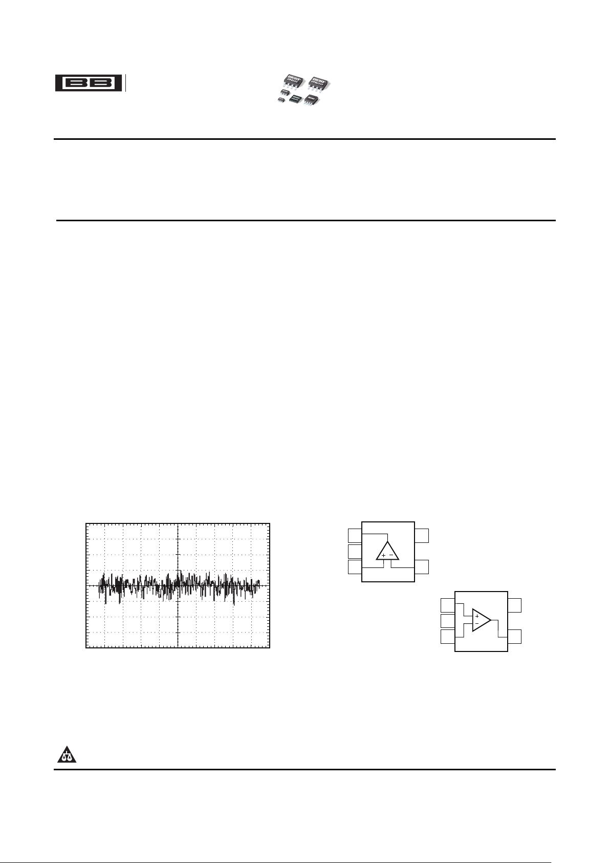
0.1HzTO10HzNOISE
500nV/div
1s/div
1
2
3
5
4
V+
-IN
OUT
V-
+IN
OPA333
SOT23-5
1
2
3
5
4
V+
OUT
+IN
V-
-IN
OPA333
SC70-5
OPA333
OPA2333
SBOS351C – MARCH 2006 – REVISED MAY 2007
1.8V, microPOWER
CMOS OPERATIONAL AMPLIFIERS
Zerø-Drift Series
• LOW OFFSET VOLTAGE: 10 μ V (max)
The OPA333 series of CMOS operational amplifiers
uses a proprietary auto-calibration technique to
• ZERO DRIFT: 0.05 μ V/ ° C (max)
simultaneously provide very low offset voltage (10 μ V
• 0.01Hz to 10Hz NOISE: 1.1 μ V
PP
max) and near-zero drift over time and temperature.
• QUIESCENT CURRENT: 17 μ A
These miniature, high-precision, low quiescent
• SINGLE-SUPPLY OPERATION current amplifiers offer high-impedance inputs that
have a common-mode range 100mV beyond the rails
• SUPPLY VOLTAGE: 1.8V to 5.5V
and rail-to-rail output that swings within 50mV of the
• RAIL-TO-RAIL INPUT/OUTPUT
rails. Single or dual supplies as low as +1.8V ( ± 0.9V)
• microSIZE PACKAGES: SC70 and SOT23
and up to +5.5V ( ± 2.75V) may be used. They are
optimized for low-voltage, single-supply operation.
The OPA333 family offers excellent CMRR without
• TRANSDUCER APPLICATIONS
the crossover associated with traditional
• TEMPERATURE MEASUREMENTS complementary input stages. This design results in
superior performance for driving analog-to-digital
• ELECTRONIC SCALES
converters (ADCs) without degradation of differential
• MEDICAL INSTRUMENTATION
linearity.
• BATTERY-POWERED INSTRUMENTS
The OPA333 (single version) is available in the
• HANDHELD TEST EQUIPMENT
SC70-5, SOT23-5, and SO-8 packages. The
OPA2333 (dual version) is offered in DFN-8 (3mm ×
3mm), MSOP-8, and SO-8 packages. All versions
are specified for operation from –40 ° C to +125 ° C.
Please be aware that an important notice concerning availability, standard warranty, and use in critical applications of Texas
Instruments semiconductor products and disclaimers thereto appears at the end of this data sheet.
PRODUCTION DATA information is current as of publication date.
Copyright © 2006–2007, Texas Instruments Incorporated
Products conform to specifications per the terms of the Texas
Instruments standard warranty. Production processing does not
necessarily include testing of all parameters.
www.ti.com
ABSOLUTE MAXIMUM RATINGS
(1)
OPA333
OPA2333
SBOS351C – MARCH 2006 – REVISED MAY 2007
This integrated circuit can be damaged by ESD. Texas Instruments recommends that all integrated circuits be handled with
appropriate precautions. Failure to observe proper handling and installation procedures can cause damage.
ESD damage can range from subtle performance degradation to complete device failure. Precision integrated circuits may be
more susceptible to damage because very small parametric changes could cause the device not to meet its published
specifications.
ORDERING INFORMATION
(1)
PRODUCT PACKAGE-LEAD PACKAGE DESIGNATOR PACKAGE MARKING
SOT23-5 DBV OAXQ
OPA333 SC70-5 DCK BQY
SO-8 D O333A
SO-8 D O2333A
OPA2333 DFN-8 DRB BQZ
MSOP-8 DGK OBAQ
(1) For the most current package and ordering information see the Package Option Addendum at the end of this document, or see the TI
web site at www.ti.com .
OPA333, OPA2333 UNIT
Supply Voltage +7 V
Signal Input Terminals, Voltage
(2)
–0.3 to (V+) + 0.3 V
Signal Input Terminals, Voltage
(2)
± 10 mA
Output Short-Circuit
(3)
Continuous
Operating Temperature –40 to +150 ° C
Storage Temperature –65 to +150 ° C
Junction Temperature +150 ° C
ESD Ratings:
Human Body Model (HBM) 4000 V
Charged Device Model (CDM) 1000 V
Machine Model (MM) 400 V
(1) Stresses above these ratings may cause permanent damage. Exposure to absolute maximum conditions for extended periods may
degrade device reliability. These are stress ratings only, and functional operation of the device at these or any other conditions beyond
those specified is not supported.
(2) Input terminals are diode-clamped to the power-supply rails. Input signals that can swing more than 0.3V beyond the supply rails should
be current limited to 10mA or less.
(3) Short-circuit to ground, one amplifier per package.
2
Submit Documentation Feedback

www.ti.com
ELECTRICAL CHARACTERISTICS: V
S
= +1.8V to +5.5V
OPA333
OPA2333
SBOS351C – MARCH 2006 – REVISED MAY 2007
Boldface limits apply over the specified temperature range, TA= –40 ° C to +125 ° C.
At TA= +25 ° C, RL= 10k Ω connected to VS/2, V
CM
= VS/2, and V
OUT
= VS/2, unless otherwise noted.
OPA333, OPA2333
PARAMETER TEST CONDITIONS MIN TYP MAX UNIT
OFFSET VOLTAGE
Input Offset Voltage V
OS
VS= +5V 2 10 μ V
vs Temperature dV
OS
/dT 0.02 0.05 μ V/ ° C
vs Power Supply PSRR VS= +1.8V to +5.5V 1 5 μ V/V
Long-Term Stability
(1)
See
(1)
Channel Separation, dc 0.1 μ V/V
INPUT BIAS CURRENT
Input Bias Current I
B
± 70 ± 200 pA
over Temperature ± 150 pA
Input Offset Current I
OS
± 140 ± 400 pA
NOISE
Input Voltage Noise, f = 0.01Hz to 1Hz 0.3 μ V
PP
Input Voltage Noise, f = 0.1Hz to 10Hz 1.1 μ V
PP
Input Current Noise, f = 10Hz i
n
100 fA/ √ Hz
INPUT VOLTAGE RANGE
Common-Mode Voltage Range V
CM
(V–) – 0.1 (V+) + 0.1 V
Common-Mode Rejection Ratio CMRR (V–) – 0.1V < VCM< (V+) + 0.1V 106 130 dB
INPUT CAPACITANCE
Differential 2 pF
Common-Mode 4 pF
OPEN-LOOP GAIN
(V–) + 100mV < VO< (V+) – 100mV, RL=
Open-Loop Voltage Gain A
OL
106 130 dB
10k Ω
FREQUENCY RESPONSE
Gain-Bandwidth Product GBW CL= 100pF 350 kHz
Slew Rate SR G = +1 0.16 V/ μ s
OUTPUT
Voltage Output Swing from Rail RL= 10k Ω 30 50 mV
over Temperature RL= 10k Ω 70 mV
Short-Circuit Current I
SC
± 5 mA
Capacitive Load Drive C
L
See Typical Characteristics
Open-Loop Output Impedance f = 350kHz, IO= 0 2 k Ω
POWER SUPPLY
Specified Voltage Range V
S
1.8 5.5 V
Quiescent Current Per Amplifier I
Q
IO= 0 17 25 μ A
over Temperature 28 μ A
Turn-On Time VS= +5V 100 μ s
TEMPERATURE RANGE
Specified Range –40 +125 ° C
Operating Range –40 +150 ° C
Storage Range –65 +150 ° C
Thermal Resistance θ
JA
° C/W
SOT23-5 200 ° C/W
MSOP-8, SO-8 150 ° C/W
DFN-8 50 ° C/W
SC70-5 250 ° C/W
(1) 300-hour life test at +150 ° C demonstrated randomly distributed variation of approximately 1 μ V.
3
Submit Documentation Feedback
www.ti.com
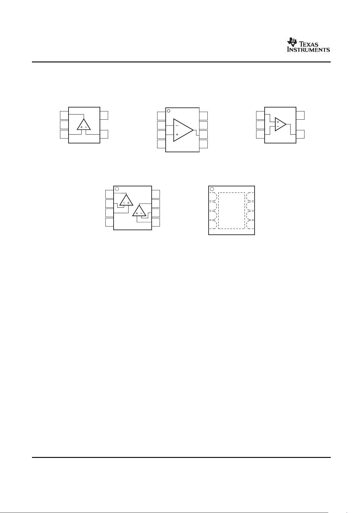
PIN CONFIGURATIONS
1
2
3
5
4
V+
-IN
OUT
V-
+IN
1
2
3
5
4
V+
OUT
+IN
V-
-IN
1
2
3
4
8
7
6
5
NC
(1)
V+
OUT
NC
(1)
NC
(1)
-IN
+IN
V-
1
2
3
4
8
7
6
5
V+
OUTB
-INB
+INB
OUTA
-INA
+INA
V-
A
B
1
2
3
4
8
7
6
5
V+
OUTB
-INB
+INB
OUTA
-INA
+INA
V-
Exposed
Thermal
DiePad
on
Underside
(2)
OPA333
OPA2333
SBOS351C – MARCH 2006 – REVISED MAY 2007
OPA333 OPA333 OPA333
SOT23-5 SO-8 SC70-5
Top View Top View Top View
OPA2333 OPA2333
SO-8, MSOP-8 DFN-8
Top View Top View
1. NC denotes no internal connection.
2. Connect thermal die pad to V–.
4
Submit Documentation Feedback
www.ti.com
TYPICAL CHARACTERISTICS
Population
-10
-9
-
8
-
7
-
6
-
5
-
4
-
3
-
2
-
1
0
1
2
3
4
5
6
7
8
9
10
OffsetVoltage( V)m
Population
0
0.0025
0.0050
0.0075
0.0100
0.0125
0.0150
0.0175
0.0200
0.0225
0.0250
0.0275
0.0300
0.0325
0.0350
0.0375
0.0400
0.0425
0.0450
0.0475
0.0500
OffsetVoltageDrift( V/ C)m °
A (dB)
OL
10
120
100
80
60
40
20
0
-20
Phase( )°
250
200
150
100
50
0
-50
-100
100k10k1k100
Frequency(Hz)
1M
Phase
Gain
CMRR(dB)
1
140
120
100
80
60
40
20
0
100k10k1k10010
Frequency(Hz)
1M
PSRR(dB)
1
120
100
80
60
40
20
0
10k 100k1k10010
Frequency(Hz)
1M
+PSRR
-PSRR
OutputSwing(V)
0
3
2
1
0
-1
-2
-3
1
OutputCurrent(mA)
107 8 965432
- °40 C
- °40 C
- °40 C
+25 C°
+25 C°
+25 C°
+125 C°
+125 C°
V = 2.75V±
S
V = 0.9V±
S
OPA333
OPA2333
SBOS351C – MARCH 2006 – REVISED MAY 2007
At TA= +25 ° C, VS= +5V, and CL= 0pF, unless otherwise noted.
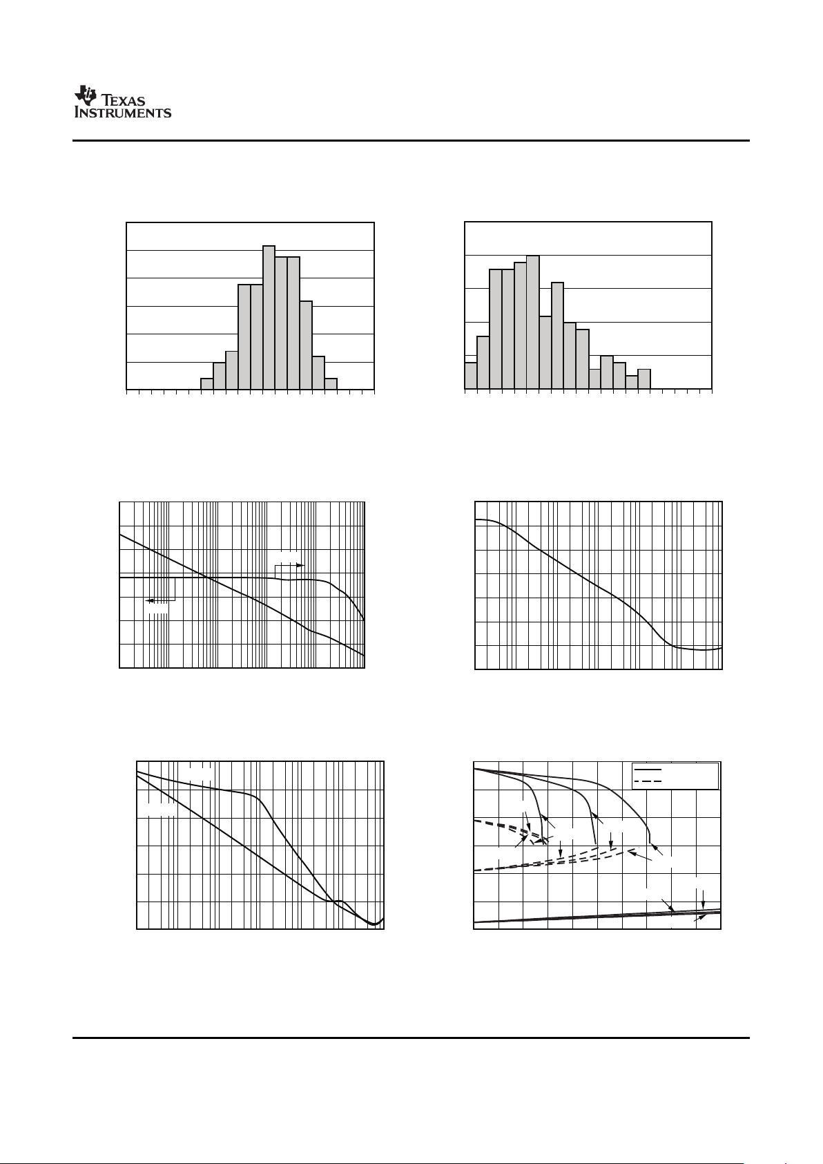
OFFSET VOLTAGE PRODUCTION DISTRIBUTION OFFSET VOLTAGE DRIFT PRODUCTION DISTRIBUTION
Figure 1. Figure 2.
OPEN-LOOP GAIN vs FREQUENCY COMMON-MODE REJECTION RATIO vs FREQUENCY
Figure 3. Figure 4.
POWER-SUPPLY REJECTION RATIO vs FREQUENCY OUTPUT VOLTAGE SWING vs OUTPUT CURRENT
Figure 5. Figure 6.
5
Submit Documentation Feedback
www.ti.com
I
(pA)
B
0
100
80
60
40
20
0
-20
-40
-60
-80
-100
1
Common-ModeVoltage(V)
5432
-I
B
+I
B
I
(pA)
B
-50
200
150
100
50
0
-50
-100
-150
-200
-25
Temperature( C)°
1251007550250
V =5.5V
S
V =1.8V
S
-I
B
-I
B
+I
B
+I
B
OutputVoltage(1V/div)
Time(50 s/div)m
G=1
R =10kW
L
I ( A)m
Q
-50
25
20
15
10
5
0
-25
Temperature( C)°
1251007550250
V =1.8V
S
V =5.5V
S
OutputVoltage(50mV/div)
Time(5 s/div)m
G=+1
R =10kW
L
2V/div
0
1V/div
0
Time(50 s/div)m
Input
Output
10kW
1kW
OPA333
+2.5V
-2.5V
OPA333
OPA2333
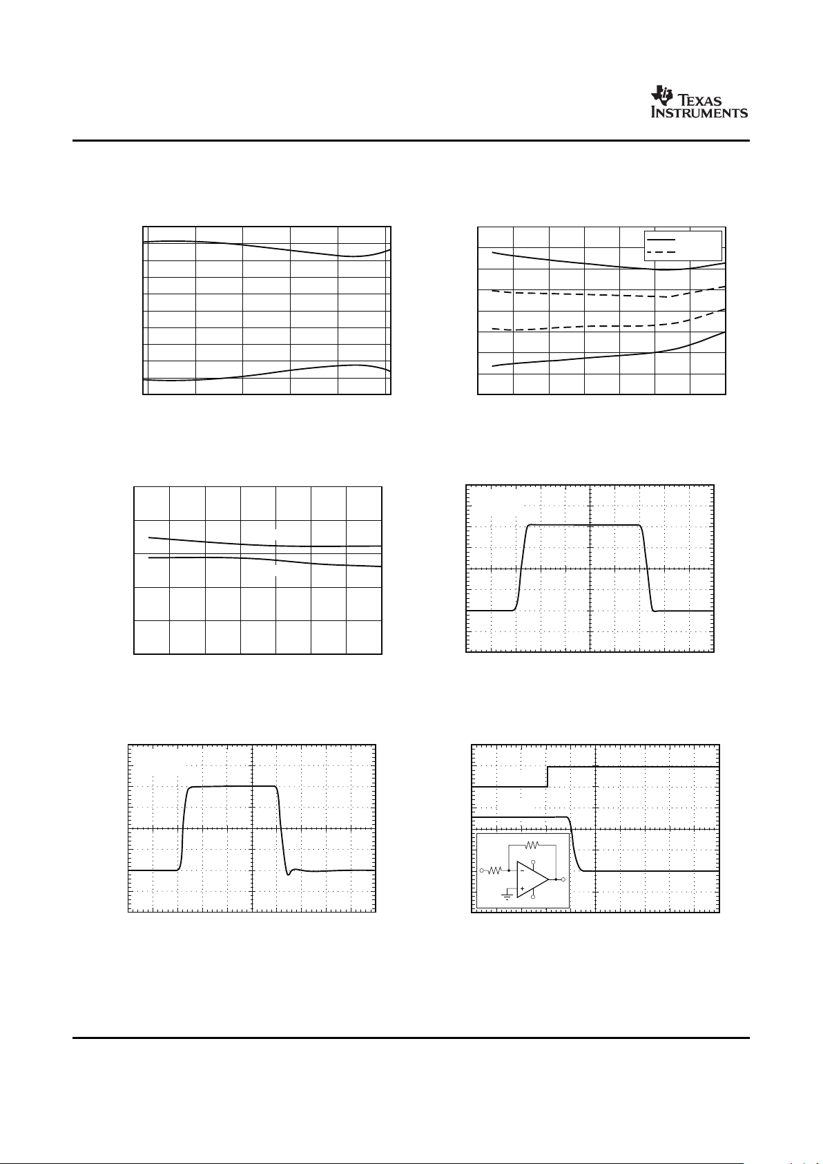
SBOS351C – MARCH 2006 – REVISED MAY 2007
TYPICAL CHARACTERISTICS (continued)
At TA= +25 ° C, VS= +5V, and CL= 0pF, unless otherwise noted.
INPUT BIAS CURRENT vs COMMON-MODE VOLTAGE INPUT BIAS CURRENT vs TEMPERATURE
Figure 7. Figure 8.
QUIESCENT CURRENT vs TEMPERATURE LARGE-SCALE STEP RESPONSE
Figure 9. Figure 10.
SMALL-SCALE STEP RESPONSE POSITIVE OVER-VOLTAGE RECOVERY
Figure 11. Figure 12.
6
Submit Documentation Feedback
www.ti.com
2V/div
0
1V/div
0
Time(50 s/div)m
Input
Output
10kW
1kW
OPA333
+2.5V
-2.5V
SettlingTime( s)
m
1
600
500
400
300
200
100
0
10
Gain(dB)
100
0.001%
0.01%
4VStep
500nV/div
1s/div
Overshoot(%)
10
40
35
30
25
20
15
10
5
0
100
LoadCapacitance(pF)
1000
VoltageNoise(nV/ )ÖHz
1
1000
100
10
CurrentNoise(fA/
)ÖHz
1000
100
10
1k10010
Frequency(Hz)
10k
CurrentNoise
VoltageNoise
Continueswithno1/f(flicker)noise.
OPA333
OPA2333
SBOS351C – MARCH 2006 – REVISED MAY 2007
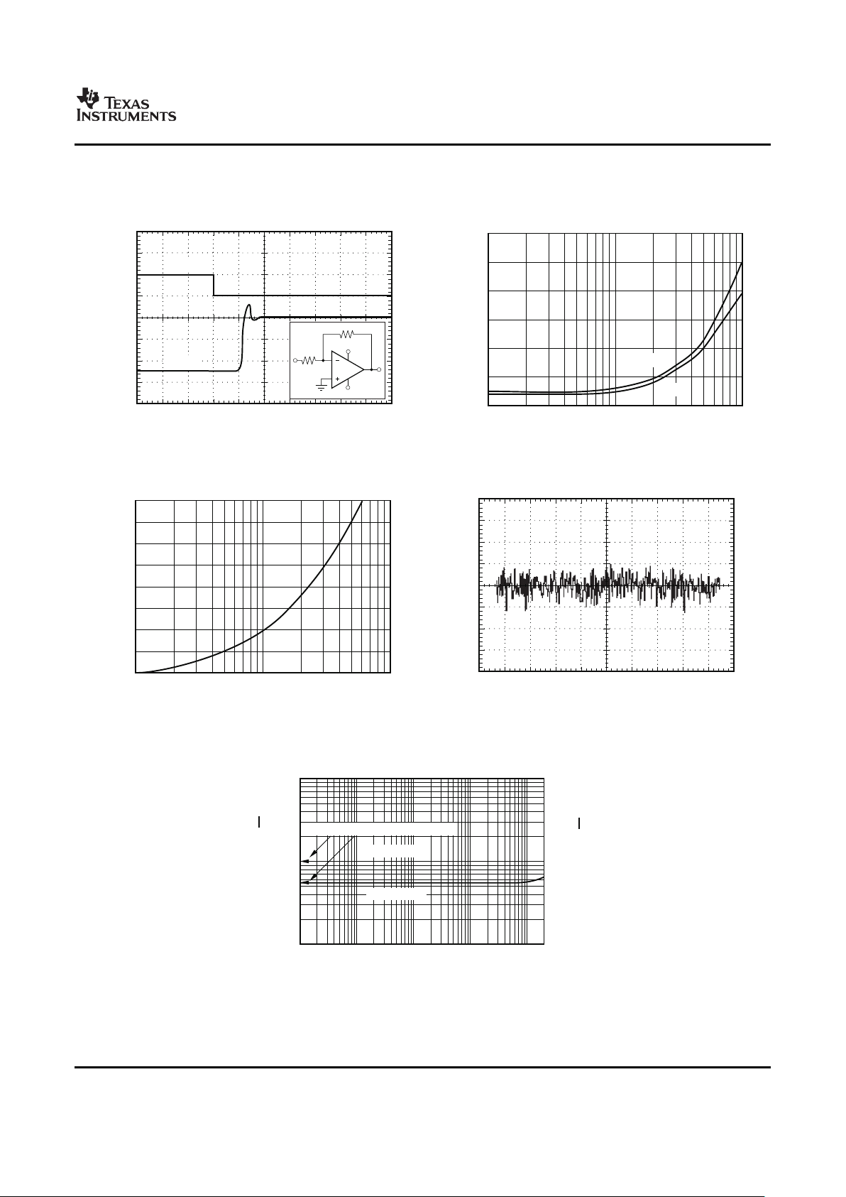
TYPICAL CHARACTERISTICS (continued)
At TA= +25 ° C, VS= +5V, and CL= 0pF, unless otherwise noted.
NEGATIVE OVER-VOLTAGE RECOVERY SETTLING TIME vs CLOSED-LOOP GAIN
Figure 13. Figure 14.
SMALL-SIGNAL OVERSHOOT vs LOAD CAPACITANCE 0.1Hz TO 10Hz NOISE
Figure 15. Figure 16.
CURRENT AND VOLTAGE NOISE SPECTRAL DENSITY vs
FREQUENCY
Figure 17.
7
Submit Documentation Feedback
 Loading...