Texas Instruments OPA369, OPA2369AIDGKT Datasheet

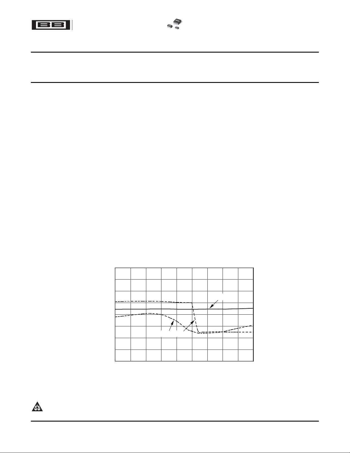
200
150
100
50
0
-50
-100
-150
-200
OFFSETVOLTAGE
vsCOMMON-MODEVOLTAGE
(V =1.8V)
S
Common-ModeVoltage(V)
OffsetVoltage( V)
m
0 0.2 0.4 0.6 0.8 1.0 1.2 1.4 1.6 1.8
Competition
OPA369
1.8V, 1 μ A max, Zerø-Crossover
RAIL-TO-RAIL I/O OPERATIONAL AMPLIFIER
1
FEATURES DESCRIPTION
2
• ZERØ-CROSSOVER
• LOW POWER: 1 μ A (max)
• LOW OFFSET VOLTAGE: 750 μ V (max)
• LOW VOLTAGE SUPPLY: +1.8V to +5.5V
• LOW OFFSET DRIFT: 1.75 μ V/ ° C (max)
• microSIZE PACKAGES:
– SC70-5, SOT23-8, MSOP-8
APPLICATIONS
• BATTERY-POWERED INSTRUMENTS
• PORTABLE DEVICES
• MEDICAL INSTRUMENTS
• TEST EQUIPMENT
OPA369
OPA2369
SBOS414A – AUGUST 2007 – REVISED SEPTEMBER 2007
The OPA369 and OPA2369 are new low-power,
low-voltage operational amplifiers from Texas
Instruments designed especially for battery-powered
applications.
The OPAx369 operates on a supply voltage as low as
1.8V and has true rail-to-rail operation that makes it
useful for a wide range of applications. The
zero-crossover feature resolves the problem of input
crossover distortion that becomes very prominent in
low voltage (< 3V), rail-to-rail input applications.
In addition to microsize packages and very low
quiescent current (1 μ A, max) the OPAx369 features
12kHz bandwidth, low offset drift (1.75 μ V/ ° C, max),
and low 0.1Hz to 10Hz noise (3.6 μ V
The OPA369 (single version, available Q4 2007) is
offered in an SC70-5 package. The OPA2369 (dual
version) comes in both MSOP-8 and SOT23-8
packages.
hi laurie
).
PP
1
Please be aware that an important notice concerning availability, standard warranty, and use in critical applications of
Texas Instruments semiconductor products and disclaimers thereto appears at the end of this data sheet.
2 All trademarks are the property of their respective owners.
PRODUCTION DATA information is current as of publication date.
Products conform to specifications per the terms of the Texas
Instruments standard warranty. Production processing does not
necessarily include testing of all parameters.
Copyright © 2007, Texas Instruments Incorporated

www.ti.com
1
2
3
5
4
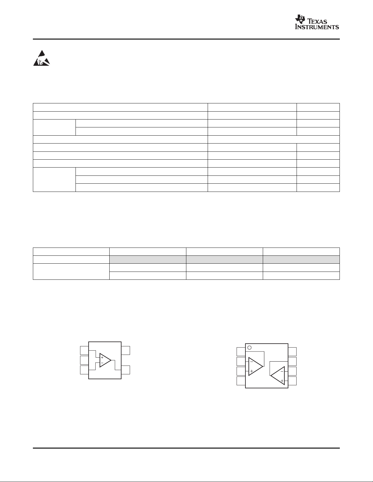
V+
OUT
+IN
V-
-IN
1
2
3
4
8
7
6
5
V+
OutB
-InB
+InB
OutA
-InA
+InA
V-
OPA369
OPA2369
SBOS414A – AUGUST 2007 – REVISED SEPTEMBER 2007
This integrated circuit can be damaged by ESD. Texas Instruments recommends that all integrated circuits be handled with
appropriate precautions. Failure to observe proper handling and installation procedures can cause damage.
ESD damage can range from subtle performance degradation to complete device failure. Precision integrated circuits may be more
susceptible to damage because very small parametric changes could cause the device not to meet its published specifications.
ABSOLUTE MAXIMUM RATINGS
(1)
Over operating free-air temperature range (unless otherwise noted).
VALUE UNIT
Supply Voltage, VS= (V+) – (V – ) +7V V
(2)
Single Input
Terminals
Output Short-Circuit
Operating Temperature, T
Storage Temperature, T
Junction Temperature, T
Voltage
(2)
Current
(3)
A
A
J
Human Body Model (HBM) 4000 V
ESD Ratings Charged Device Model (CDM) 1000 V
Machine Model (MM) 200 V
(1) Stresses above these ratings may cause permanent damage. Exposure to absolute maximum conditions for extended periods may
degrade device reliability. These are stress ratings only, and functional operation of the device at these or any other conditions beyond
those specified is not supported.
(2) Input terminals are diode-clamped to the power-supply rails. Input signals that can swing more than 0.5V beyond the supply rails should
be current limited to 10mA or less.
(3) Short-circuit to VS/2, one amplifier per package.
PACKAGE/ORDERING INFORMATION
PRODUCT PACKAGE-LEAD PACKAGE DESIGNATOR PACKAGE MARKING
OPA369 SC70-5
OPA2369
(1) For the most current package and ordering information see the Package Option Addendum at the end of this document, or see the TI
web site at www.ti.com .
(2) Available Q4, 2007.
(2)
MSOP-8 DGK OCCQ
SOT23-8 DCN OCBQ
– 0.5 to (V+) + 0.5 V
± 10 mA
Continuous
– 55 to +125 ° C
– 65 to +150 ° C
+150 ° C
(1)
DCK CJS
PIN CONFIGURATIONS
OPA369
(TOP VIEW)
(1) Available Q4, 2007.
2 Submit Documentation Feedback Copyright © 2007, Texas Instruments Incorporated
(1)
SC70-5
OPA2369
MSOP-8, SOT23-8
(TOP VIEW)
Product Folder Link(s): OPA369 OPA2369

www.ti.com
OPA369
OPA2369
SBOS414A – AUGUST 2007 – REVISED SEPTEMBER 2007
ELECTRICAL CHARACTERISTICS: V
= +1.8V to +5.5V
S
BOLDFACE limits apply over the specified temperature range, TA= – 40 ° C to +85 ° C.
At TA= +25 ° C, RL= 100k Ω connected to VS/2, unless otherwise noted.
(1)
OPA369
PARAMETER CONDITIONS MIN TYP MAX UNIT
OFFSET VOLTAGE
Input Offset Voltage V
OS
over Temperature 1 mV
Drift dV
/dT 0.4 1.75 μ V/ ° C
OS
vs Power Supply PSRR VS= 1.8V to 5.5V 5 20 μ V/V
Channel Separation dc 0.1 μ V/V
f = 1kHz 120 dB
INPUT VOLTAGE RANGE
Common-Mode Voltage Range V
CM
(V – ) (V+) V
Common-Mode Rejection Ratio CMRR (V – ) ≤ VCM≤ (V+) 100 114 dB
over Temperature (V – ) ≤ VCM≤ (V+) 90 dB
INPUT BIAS CURRENT
Input Bias Current I
Input Offset Current I
B
OS
INPUT IMPEDANCE
Differential
Common-Mode
NOISE
Input Voltage Noise f = 0.1Hz to 10Hz 3.6 μ V
Input Voltage Noise Density f = 100Hz 160 nV/ √ Hz
f = 1kHz 120 nV/ √ Hz
Current Noise Density f = 1kHz 1 fA/ √ Hz
OPEN-LOOP GAIN
Open-Loop Voltage Gain A
Over Temperature 100mV ≤ VO≤ (V+) – 100mV, RL=
Over Temperature 500mV ≤ VO≤ (V+) – 500mV, RL=
100mV ≤ VO≤ (V+) – 100mV, RL=
OL
100k Ω
100k Ω
500mV ≤ VO≤ (V+) – 500mV, RL=
114 134 dB
100 dB
10k Ω
10k Ω
114 134 dB
90 d B
OUTPUT
Voltage Output Swing from Rail RL= 100k Ω 10 mV
RL= 10k Ω 25 mV
Short-Circuit Current I
Capacitive Load Drive C
SC
LOAD
See Typical Characteristics pF
FREQUENCY RESPONSE
Gain-Bandwidth Product GBW 12 kHz
Slew Rate SR G = +1 0.005 V/ μ s
Overload Recovery Time VIN× Gain > V
S
POWER SUPPLY
Specified Voltage V
Quiescent Current
(per channel amplifier)
S
I
Q
I
= 0A 0.7 1 μ A
OUT
1.8 5.5 V
Over Temperature 1.25 μ A
(1) OPA369 specifications are preview. Available Q4, 2007.
, OPA2369
250 750 μ V
10 50 pA
10 50 pA
13
10
|| 3
13
10
|| 6
10 mA
250 μ s
Ω || pF
Ω || pF
PP
Copyright © 2007, Texas Instruments Incorporated Submit Documentation Feedback 3
Product Folder Link(s): OPA369 OPA2369

www.ti.com
OPA369
OPA2369
SBOS414A – AUGUST 2007 – REVISED SEPTEMBER 2007
ELECTRICAL CHARACTERISTICS: V
= +1.8V to +5.5V (continued)
S
BOLDFACE limits apply over the specified temperature range, TA= – 40 ° C to +85 ° C.
At TA= +25 ° C, RL= 100k Ω connected to VS/2, unless otherwise noted.
(1)
OPA369
PARAMETER CONDITIONS MIN TYP MAX UNIT
TEMPERATURE RANGE
Specified Range T
Operating Range T
Thermal Resistance θ
SC70 250 ° C/W
SOT23 223 ° C/W
MSOP 252 ° C/W
JA
A
A
– 40 +85 ° C
– 55 +125 ° C
, OPA2369
4 Submit Documentation Feedback Copyright © 2007, Texas Instruments Incorporated
Product Folder Link(s): OPA369 OPA2369

www.ti.com
Population
OffsetVoltage( V)m
-750
-
675
-600
-525
-450
-
375
-300
-225
-
150
-75
0
75
150
225
300
375
450
525
600
675
750
-1.2
Population
OffsetVoltageDrift( V/ C)m °
-1.1
-1.0
-0.9
-0.8
-0.7
-0.6
-0.5
-0.4
-0.3
-0.2
-0.1
0
0.1
0.2
0.3
0.4
0.5
0.6
0.7
0.8
0.9
1.0
1.1
1.2
1000
800
600
400
200
0
-200
-400
-600
-800
-1000
Temperature( C)°
OffsetVoltage( V)m
-75 100 125-50 -25 0 25 50 75
Normalized OffsetVoltage m( V)
100
80
60
40
20
0
-20
-40
-60
-80
-100
Common-ModeVoltage (V)
-0.2
0
0.2
0.4
0.6
0.8
1.0
1.2
1.4
1.6
1.8
2.0
2.2
2.4
2.6
2.8
3.0
3.2
3.4
3.6
3.8
4.0
4.2
4.4
4.6
4.8
5.0
5.2
V =5V
S
10TypicalUnitsShown
1m
V/div
Time(500ms/div)
10000
1000
100
10
Frequency(Hz)
V
oltageNoise,RTI(nV/ )
ÖHz
0.1 100101 1k
SBOS414A – AUGUST 2007 – REVISED SEPTEMBER 2007
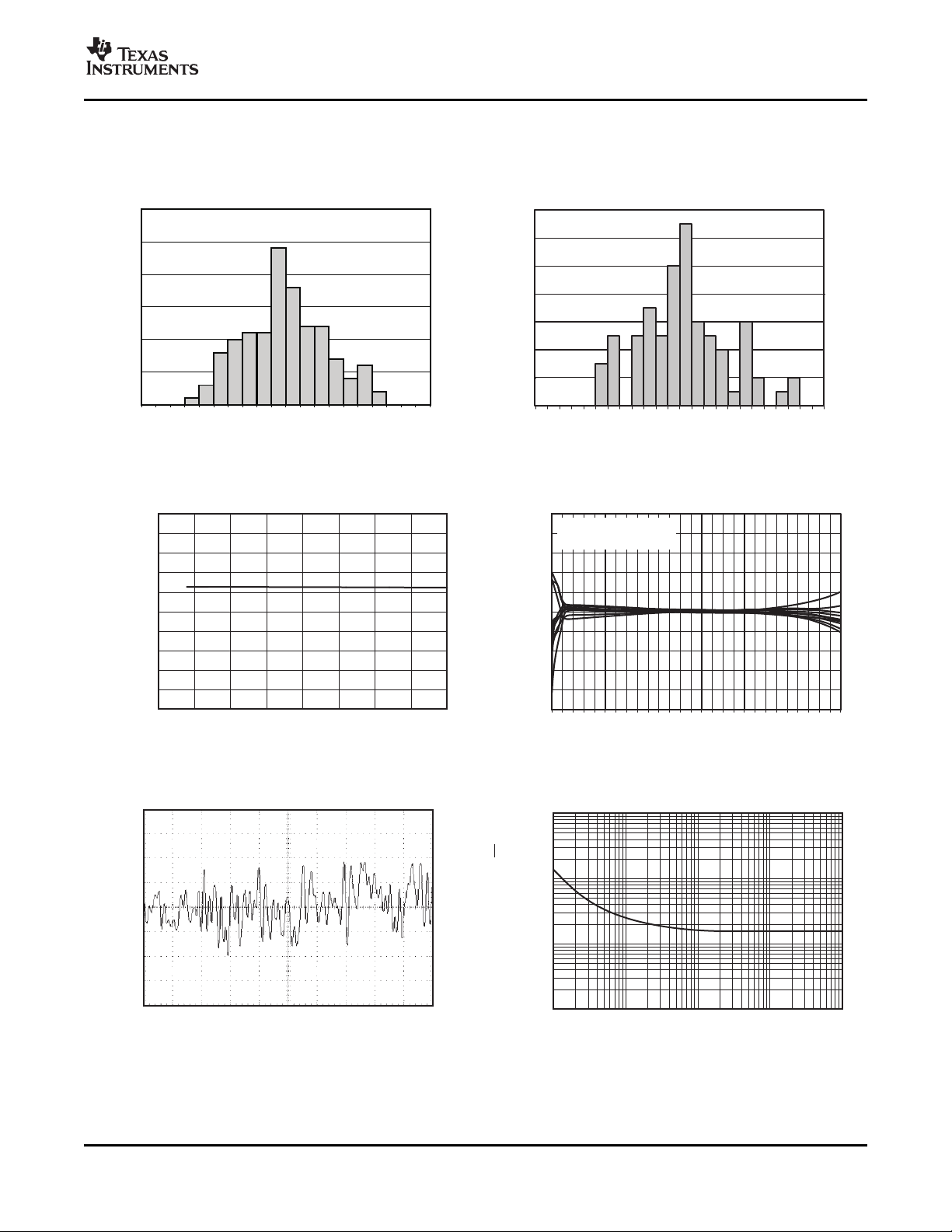
TYPICAL CHARACTERISTICS
At TA= +25 ° C, VS= 5V, RL= 100k Ω connected to VS/2, unless otherwise noted.
OFFSET VOLTAGE OFFSET VOLTAGE DRIFT
PRODUCTION DISTRIBUTION PRODUCTION DISTRIBUTION
Figure 1. Figure 2.
OPA369
OPA2369
OFFSET VOLTAGE vs TEMPERATURE vs COMMON-MODE VOLTAGE
NORMALIZED OFFSET VOLTAGE
Figure 3. Figure 4.
INPUT-REFERRED VOLTAGE NOISE
0.1Hz to 10Hz NOISE vs FREQUENCY
Copyright © 2007, Texas Instruments Incorporated Submit Documentation Feedback 5
Figure 5. Figure 6.
Product Folder Link(s): OPA369 OPA2369

www.ti.com
140
120
100
80
60
40
20
0
-20
Frequency(Hz)
Gain(dB)
0.001 100 1k100.1 10.01 20k10k
PHASE
GAIN
180
135
90
45
0
Phase( )
°
110
100
90
80
70
60
50
40
30
20
10
0
Frequency(Hz)
PSRR(dB)
1 1k 10k10010 20k
+PSRR
-PSRR
120
100
80
60
40
20
0
Frequency(Hz)
CMRR(dB)
10 10k1k100 20k
160
140
120
100
80
60
40
20
0
Frequency(Hz)
ChannelSeparation(dB)
100 10k1k 100k
20
15
10
5
0
-5
-10
-15
-20
Temperature( C)°
PSRR( V/V)m
-75 -50 -25 0 25 50 75 100 125
10TypicalUnitsShown
10
8
6
4
2
0
Temperature( C)°
CMRR( V/V)m
-75 100 125-50 -25 0 25 50 75
OPA369
OPA2369
SBOS414A – AUGUST 2007 – REVISED SEPTEMBER 2007
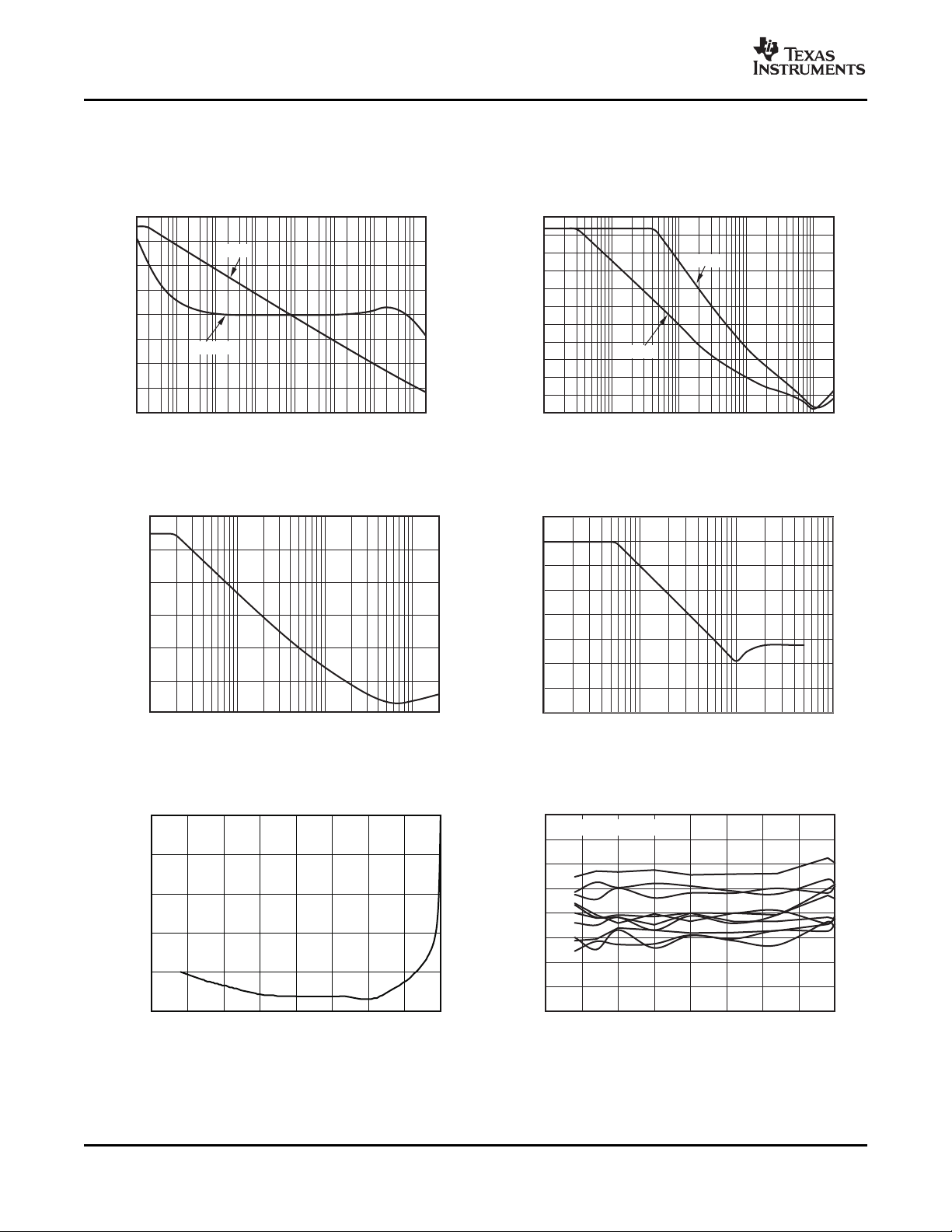
TYPICAL CHARACTERISTICS (continued)
At TA= +25 ° C, VS= 5V, RL= 100k Ω connected to VS/2, unless otherwise noted.
OPEN-LOOP GAIN AND PHASE POWER-SUPPLY REJECTION RATIO
vs FREQUENCY vs FREQUENCY
Figure 7. Figure 8.
COMMON-MODE REJECTION RATIO
vs FREQUENCY CHANNEL SEPARATION vs FREQUENCY
Figure 9. Figure 10.
COMMON-MODE REJECTION RATIO POWER-SUPPLY REJECTION RATIO
vs TEMPERATURE vs TEMPERATURE
6 Submit Documentation Feedback Copyright © 2007, Texas Instruments Incorporated
Figure 11. Figure 12.
Product Folder Link(s): OPA369 OPA2369
 Loading...