Texas Instruments OPA171AID, OPA171AIDBVT, OPA171AIDRLT, OPA2171AID, OPA2171AIDCUT Schematic [ru]
...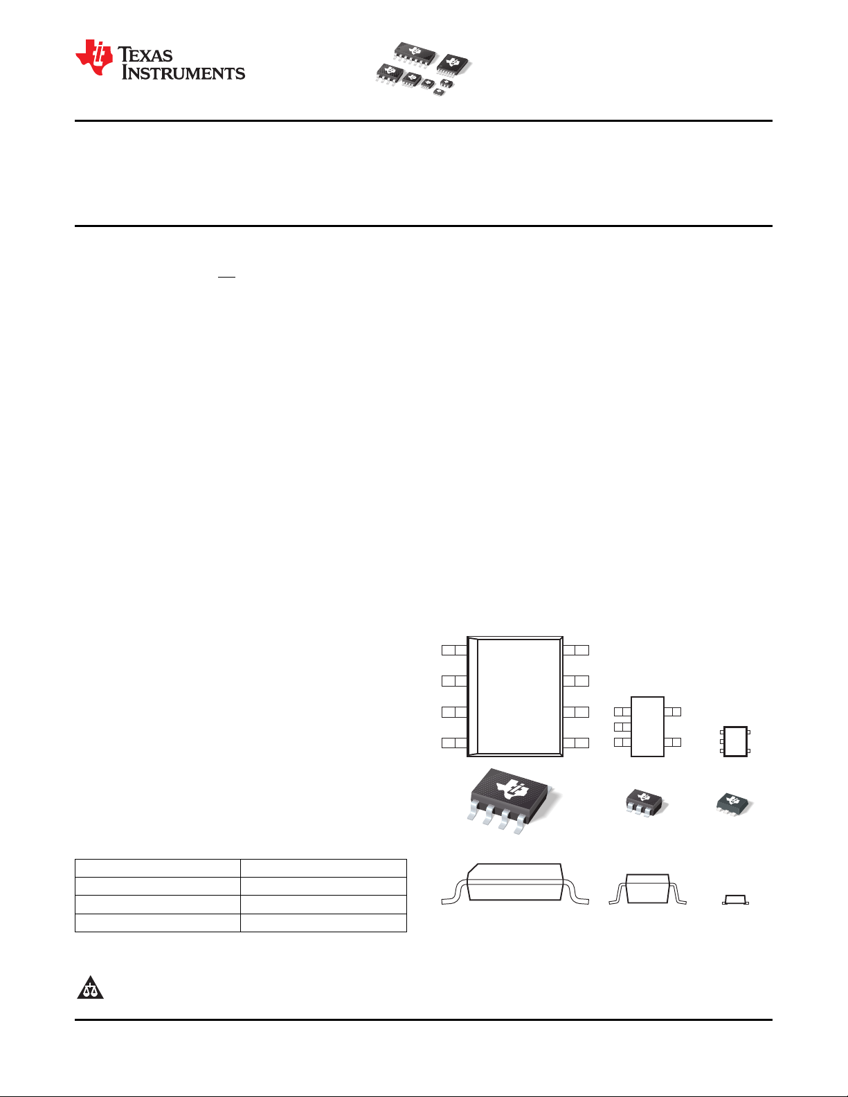
PackageFootprintComparison(toScale)
PackageHeight (toScale)Comparison
D(SO-8) DBV(SOT23-5) DRL(SOT553)
www.ti.com
36V, Single-Supply, SOT553, General-Purpose
OPERATIONAL AMPLIFIERS
Value Line Series
Check for Samples: OPA171, OPA2171, OPA4171
1
FEATURES
• Supply Range: +2.7V to +36V, ±1.35V to ±18V
• Low Noise: 14nV/√Hz
• Low Offset Drift: ±0.3µV/°C (typ)
• RFI Filtered Inputs
• Input Range Includes the Negative Supply
• Input Range Operates to Positive Supply
• Rail-to-Rail Output
• Gain Bandwidth: 3MHz
• Low Quiescent Current: 475µA per Amplifier
• High Common-Mode Rejection: 120dB (typ)
• Low Input Bias Current: 8pA
• Industry-Standard Packages:
– 8-Pin SOIC
– 8-Pin MSOP
– 14-Pin TSSOP
• microPackages:
– Single in SOT553
– Dual in VSSOP-8
OPA171
OPA2171
OPA4171
SBOS516D –SEPTEMBER 2010–REVISED SEPTEMBER 2012
DESCRIPTION
The OPA171, OPA2171 and OPA4171 (OPAx171)2
are a family of 36V, single-supply, low-noise
operational amplifiers with the ability to operate on
supplies ranging from +2.7V (±1.35V) to +36V
(±18V). These devices are available in micropackages and offer low offset, drift, and bandwidth
with low quiescent current. The single, dual, and
quad versions all have identical specifications for
maximum design flexibility.
Unlike most op amps, which are specified at only one
supply voltage, the OPAx171 family is specified from
+2.7V to +36V. Input signals beyond the supply rails
do not cause phase reversal. The OPAx171 family is
stable with capacitive loads up to 300pF. The input
can operate 100mV below the negative rail and within
2V of the top rail during normal operation. Note that
these devices can operate with full rail-to-rail input
100mV beyond the top rail, but with reduced
performance within 2V of the top rail.
The OPAx171 series of op amps are specified from
–40°C to +125°C.
APPLICATIONS
• Tracking Amplifier in Power Modules
• Merchant Power Supplies
• Transducer Amplifiers
• Bridge Amplifiers
• Temperature Measurements
• Strain Gauge Amplifiers
• Precision Integrators
• Battery-Powered Instruments
• Test Equipment
Product Family
DEVICE PACKAGE
OPA171 SOT553, SOT23-5, SO-8
OPA2171 (dual) VSSOP-8, SO-8, MSOP-8
OPA4171 (quad) TSSOP-14, SO-14
1
Please be aware that an important notice concerning availability, standard warranty, and use in critical applications of
Texas Instruments semiconductor products and disclaimers thereto appears at the end of this data sheet.
2All trademarks are the property of their respective owners.
PRODUCTION DATA information is current as of publication date.
Products conform to specifications per the terms of the Texas
Instruments standard warranty. Production processing does not
necessarily include testing of all parameters.
Smallest Packaging for 36V Op Amps
Copyright © 2010–2012, Texas Instruments Incorporated
OPA171
OPA2171
OPA4171
SBOS516D –SEPTEMBER 2010–REVISED SEPTEMBER 2012
This integrated circuit can be damaged by ESD. Texas Instruments recommends that all integrated circuits be handled with
appropriate precautions. Failure to observe proper handling and installation procedures can cause damage.
ESD damage can range from subtle performance degradation to complete device failure. Precision integrated circuits may be more
susceptible to damage because very small parametric changes could cause the device not to meet its published specifications.
www.ti.com
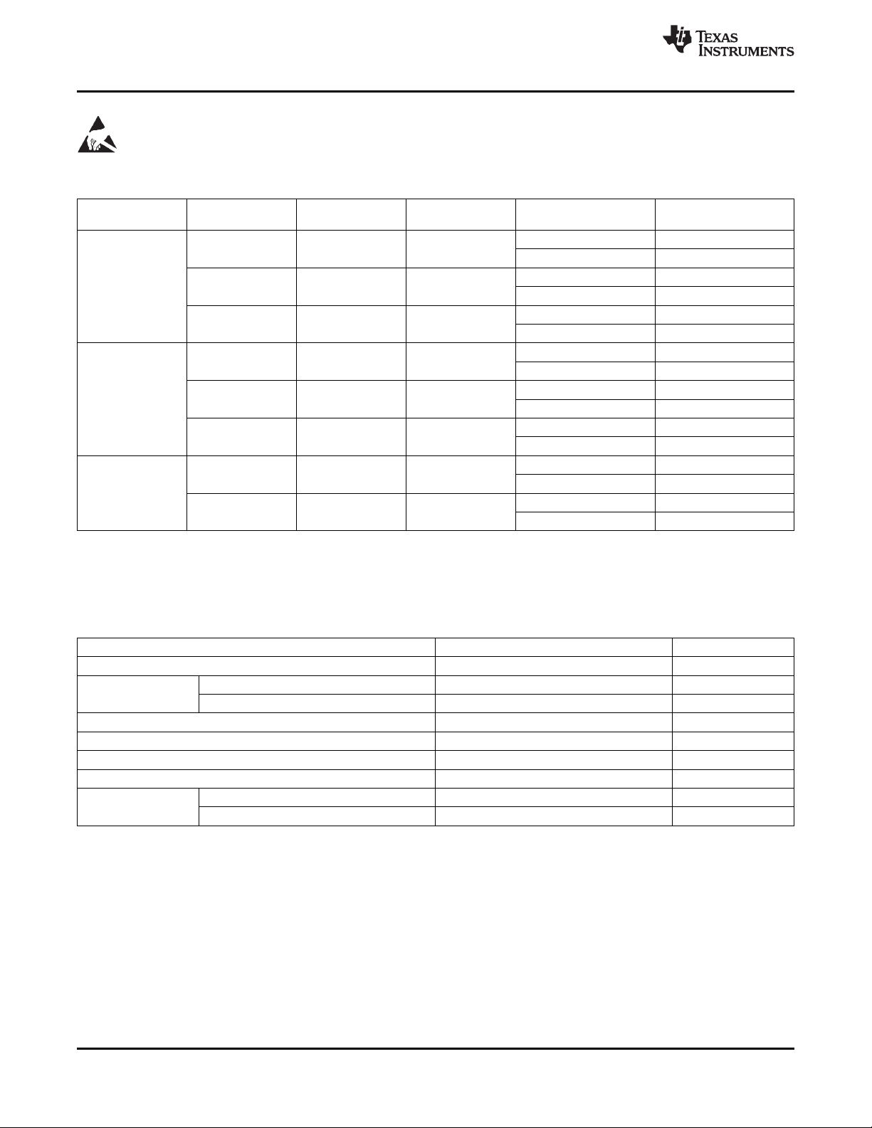
PACKAGE/ORDERING INFORMATION
PACKAGE PACKAGE TRANSPORT MEDIA,
PRODUCT PACKAGE-LEAD DESIGNATOR MARKING ORDERING NUMBER QUANTITY
SOT553 DRL DAP
OPA171 SOT23-5 DBV OSUI
SO-8 D O171A
MSOP-8 DGK OPMI
OPA2171 VSSOP-8 DCU OPOC
SO-8 D 2171A
SO-14 D OPA4171
OPA4171
TSSOP-14 PW OPA4171
(1) For the most current package and ordering information, see the Package Option Addendum at the end of this document, or visit the
device product folder at www.ti.com.
(1)
OPA171AIDRLT Tape and Reel, 250
OPA171AIDRLR Tape and Reel, 4000
OPA171AIDBVT Tape and Reel, 250
OPA171AIDBVR Tape and Reel, 3000
OPA171AID Rail, 75
OPA171AIDR Tape and Reel, 2500
OPA2171AIDGK Rail, 80
OPA2171AIDGKR Tape and Reel, 2500
OPA2171AIDCUT Tape and Reel, 250
OPA2171AIDCUR Tape and Reel, 3000
OPA2171AID Rail, 75
OPA2171AIDR Tape and Reel, 2500
OPA4171AID Rail, 50
OPA4171AIDR Tape and Reel, 2500
OPA4171AIPW Rail, 90
OPA4171AIPWR Tape and Reel, 2000
ABSOLUTE MAXIMUM RATINGS
(1)
Over operating free-air temperature range, unless otherwise noted.
OPAx171 UNIT
Supply voltage ±20 V
Signal input terminals
Output short circuit
Operating temperature –55 to +150 °C
Storage temperature –65 to +150 °C
Junction temperature +150 °C
ESD ratings:
(1) Stresses above these ratings may cause permanent damage. Exposure to absolute maximum conditions for extended periods may
degrade device reliability. These are stress ratings only, and functional operation of the device at these or any other conditions beyond
those specified is not implied.
(2) Short-circuit to ground, one amplifier per package.
Voltage (V–) – 0.5 to (V+) + 0.5 V
Current ±10 mA
(2)
Human body model (HBM) 4 kV
Charged device model (CDM) 750 V
Continuous
2 Submit Documentation Feedback Copyright © 2010–2012, Texas Instruments Incorporated
Product Folder Links: OPA171 OPA2171 OPA4171
OPA171
OPA2171
OPA4171
www.ti.com
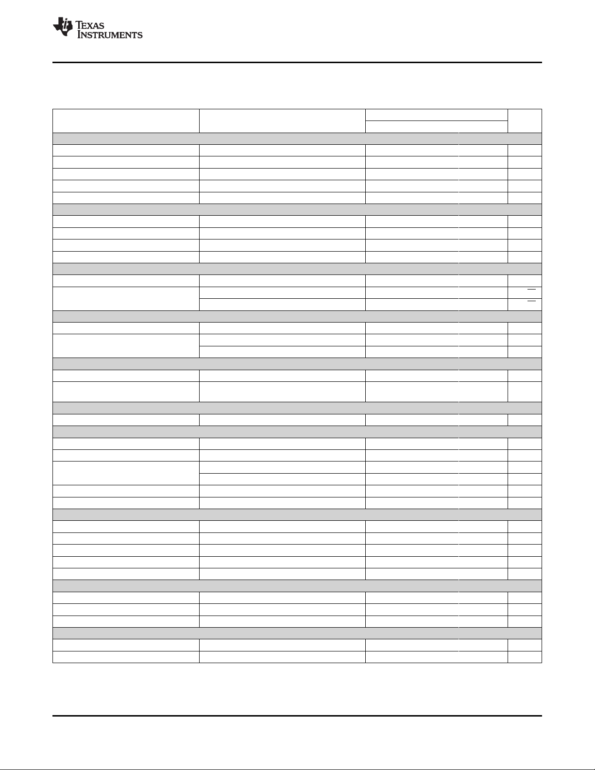
ELECTRICAL CHARACTERISTICS
Boldface limits apply over the specified temperature range, TA= –40°C to +125°C.
At TA= +25°C, VS= +2.7V to +36V, VCM= V
PARAMETER TEST CONDITIONS MIN TYP MAX UNIT
OFFSET VOLTAGE
Input offset voltage V
Over temperature 0.3 ±2 mV
Drift dVOS/dT 0.3 ±2 µV/°C
vs power supply PSRR VS= +4V to +36V 1 ±3 µV/V
Channel separation, dc dc 5 µV/V
INPUT BIAS CURRENT
Input bias current I
Over temperature ±3.5 nA
Input offset current I
Over temperature ±3.5 nA
NOISE
Input voltage noise f = 0.1Hz to 10Hz 3 µV
Input voltage noise density e
INPUT VOLTAGE
Common-mode voltage range
Common-mode rejection ratio CMRR
INPUT IMPEDANCE
Differential 100 || 3 MΩ || pF
Common-mode 6 || 3
OPEN-LOOP GAIN
Open-loop voltage gain AOLVS= +4V to +36V, (V–) + 0.35V < VO< (V+) – 0.35V 110 130 dB
FREQUENCY RESPONSE
Gain bandwidth product GBP 3.0 MHz
Slew rate SR G = +1 1.5 V/µs
Settling time t
Overload recovery time VIN× Gain > V
Total harmonic distortion + noise THD+N G = +1, f = 1kHz, VO= 3V
OUTPUT
Voltage output swing from rail V
Over temperature RL= 10kΩ, AOL≥ 110dB (V–) + 0.35 (V+) – 0.35 V
Short-circuit current I
Capacitive load drive C
Open-loop output resistance R
POWER SUPPLY
Specified voltage range V
Quiescent current per amplifier I
Over temperature IO= 0A 650 µA
TEMPERATURE
Specified range –40 +125 °C
Operating range –55 +150 °C
(1)
(1) The input range can be extended beyond (V+) – 2V up to V+. See the Typical Characteristics and Application Information sections for
additional information.
OS
B
OS
n
V
CM
S
To 0.01% (12 bit), VS= ±18V, G = +1, 10V step 10 µs
O
SC
LOAD
O
S
Q
= VS/2, and R
OUT
f = 100Hz 25 nV/√Hz
f = 1kHz 14 nV/√Hz
VS= ±2V, (V–) – 0.1V < VCM< (V+) – 2V 90 104 dB
VS= ±18V, (V–) – 0.1V < VCM< (V+) – 2V 104 120 dB
To 0.1%, VS= ±18V, G = +1, 10V step 6 µs
VS= 5V, RL= 10kΩ 30 mV
f = 1MHz, IO= 0A 150 Ω
IO= 0A 475 595 µA
= 10kΩ connected to VS/2, unless otherwise noted.
LOAD
S
SBOS516D –SEPTEMBER 2010–REVISED SEPTEMBER 2012
OPA171, OPA2171, OPA4171
0.25 ±1.8 mV
±8 ±15 pA
±4 pA
(V–) – 0.1V (V+) – 2V V
2 µs
RMS
See Typical Characteristics pF
+2.7 +36 V
0.0002 %
+25/–35 mA
1012Ω ||
pF
PP
Copyright © 2010–2012, Texas Instruments Incorporated Submit Documentation Feedback 3
Product Folder Links: OPA171 OPA2171 OPA4171

OPA171
OPA2171
OPA4171
SBOS516D –SEPTEMBER 2010–REVISED SEPTEMBER 2012
THERMAL INFORMATION: OPA171
THERMAL METRIC
(1)
D (SO) DBV (SOT23) DRL (SOT553) UNITS
8 PINS 5 PINS 5 PINS
θ
JA
θ
JC(top)
θ
JB
ψ
JT
ψ
JB
θ
JC(bottom)
Junction-to-ambient thermal resistance 149.5 245.8 208.1
Junction-to-case(top) thermal resistance 97.9 133.9 0.1
Junction-to-board thermal resistance 87.7 83.6 42.4
Junction-to-top characterization parameter 35.5 18.2 0.5
Junction-to-board characterization parameter 89.5 83.1 42.2
Junction-to-case(bottom) thermal resistance N/A N/A N/A
(1) For more information about traditional and new thermal metrics, see the IC Package Thermal Metrics application report, SPRA953.
OPA171
THERMAL INFORMATION: OPA2171
THERMAL METRIC
(1)
D (SO) DCU (VSSOP) DGK (MSOP) UNITS
8 PINS 8 PINS 8 PINS
θ
JA
θ
JC(top)
θ
JB
ψ
JT
ψ
JB
θ
JC(bottom)
Junction-to-ambient thermal resistance 134.3 175.2 195.3
Junction-to-case(top) thermal resistance 72.1 74.9 59.4
Junction-to-board thermal resistance 60.6 22.2 115.1
Junction-to-top characterization parameter 18.2 1.6 4.7
Junction-to-board characterization parameter 53.8 22.8 114.4
Junction-to-case(bottom) thermal resistance N/A N/A N/A
(1) For more information about traditional and new thermal metrics, see the IC Package Thermal Metrics application report, SPRA953.
OPA2171
www.ti.com
°C/W
°C/W
THERMAL INFORMATION: OPA4171
THERMAL METRIC
(1)
D (SO) PW (TSSOP) UNITS
14 PINS 14 PINS
θ
JA
θ
JC(top)
θ
JB
ψ
JT
ψ
JB
θ
JC(bottom)
Junction-to-ambient thermal resistance 93.2 106.9
Junction-to-case(top) thermal resistance 51.8 24.4
Junction-to-board thermal resistance 49.4 59.3
Junction-to-top characterization parameter 13.5 0.6
Junction-to-board characterization parameter 42.2 54.3
Junction-to-case(bottom) thermal resistance N/A N/A
(1) For more information about traditional and new thermal metrics, see the IC Package Thermal Metrics application report, SPRA953.
OPA4171
°C/W
4 Submit Documentation Feedback Copyright © 2010–2012, Texas Instruments Incorporated
Product Folder Links: OPA171 OPA2171 OPA4171
1
2
3
4
8
7
6
5
NC
(1)
V+
OUT
NC
(1)
NC
(1)
-IN
+IN
V-
1
2
3
4
14
13
12
11
OUTD
-IND
+IND
V-
OUTA
-INA
+INA
V+
5
6
7
10
9
8
+INC
-INC
OUTC
+INB
-INB
OUTB
1
2
3
5
4
V+
-IN
OUT
V-
+IN
1
2
3
4
8
7
6
5
V+
OUTB
-INB
+INB
OUTA
-INA
+INA
V-
1
2
3
5
4
V+
OUT
IN+
V-
IN-
www.ti.com
OPA171
OPA2171
OPA4171
SBOS516D –SEPTEMBER 2010–REVISED SEPTEMBER 2012
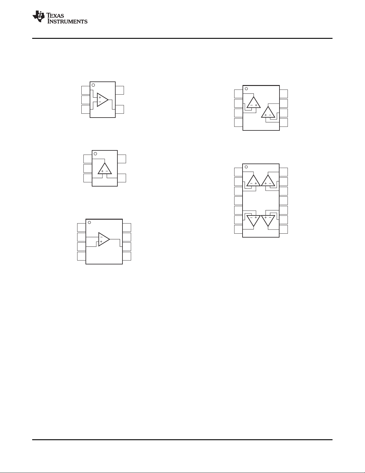
PIN CONFIGURATIONS
DRL PACKAGE: OPA171
SOT-553
(TOP VIEW)
DBV PACKAGE: OPA171
SOT23-5
(TOP VIEW)
D PACKAGE: OPA171
SO-8
(TOP VIEW)
D, DCU, AND DGK PACKAGES: OPA2171
SO-8, VSSOP-8, AND MSOP-8
(TOP VIEW)
D AND PW PACKAGES: OPA4171
SO-14 AND TSSOP-14
(TOP VIEW)
(1) No internal connection.
Product Folder Links: OPA171 OPA2171 OPA4171
Copyright © 2010–2012, Texas Instruments Incorporated Submit Documentation Feedback 5

OPA171
OPA2171
OPA4171
SBOS516D –SEPTEMBER 2010–REVISED SEPTEMBER 2012
TYPICAL CHARACTERISTICS
Table 1. Characteristic Performance Measurements
DESCRIPTION FIGURE
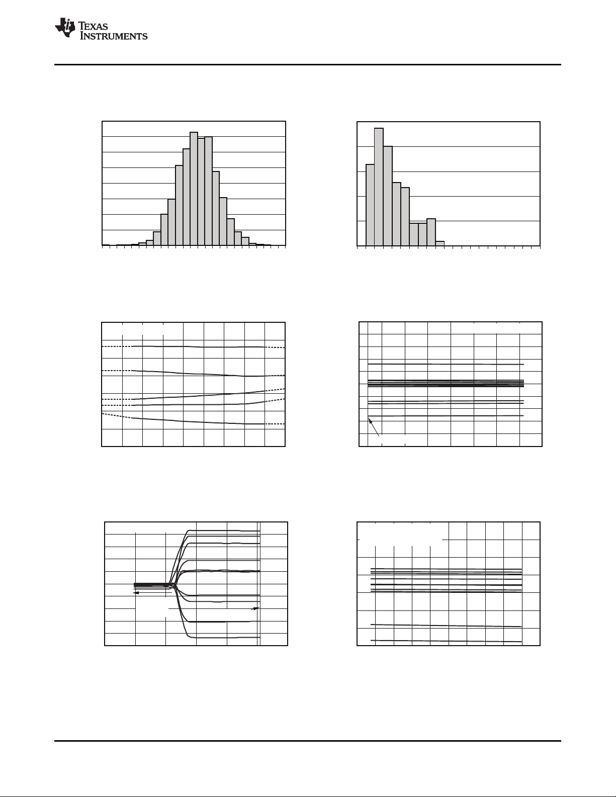
Offset Voltage Production Distribution Figure 1
Offset Voltage Drift Distribution Figure 2
Offset Voltage vs Temperature Figure 3
Offset Voltage vs Common-Mode Voltage Figure 4
Offset Voltage vs Common-Mode Voltage (Upper Stage) Figure 5
Offset Voltage vs Power Supply Figure 6
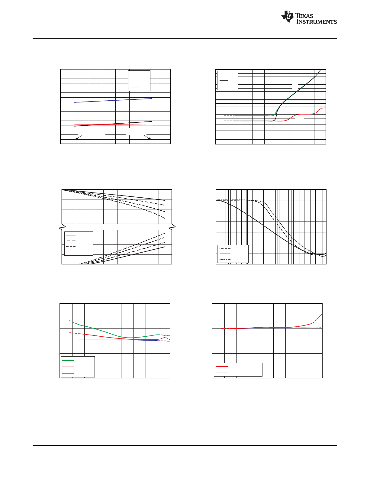
IBand IOSvs Common-Mode Voltage Figure 7
Input Bias Current vs Temperature Figure 8
Output Voltage Swing vs Output Current (Maximum Supply) Figure 9
CMRR and PSRR vs Frequency (Referred-to Input) Figure 10
CMRR vs Temperature Figure 11
PSRR vs Temperature Figure 12
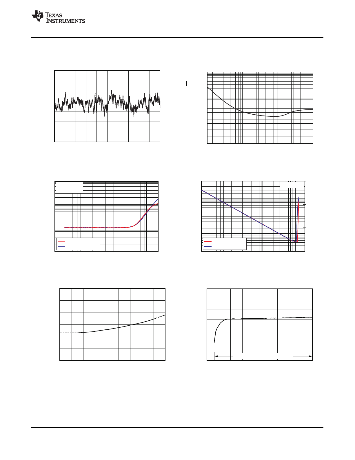
0.1Hz to 10Hz Noise Figure 13
Input Voltage Noise Spectral Density vs Frequency Figure 14
THD+N Ratio vs Frequency Figure 15
THD+N vs Output Amplitude Figure 16
Quiescent Current vs Temperature Figure 17
Quiescent Current vs Supply Voltage Figure 18
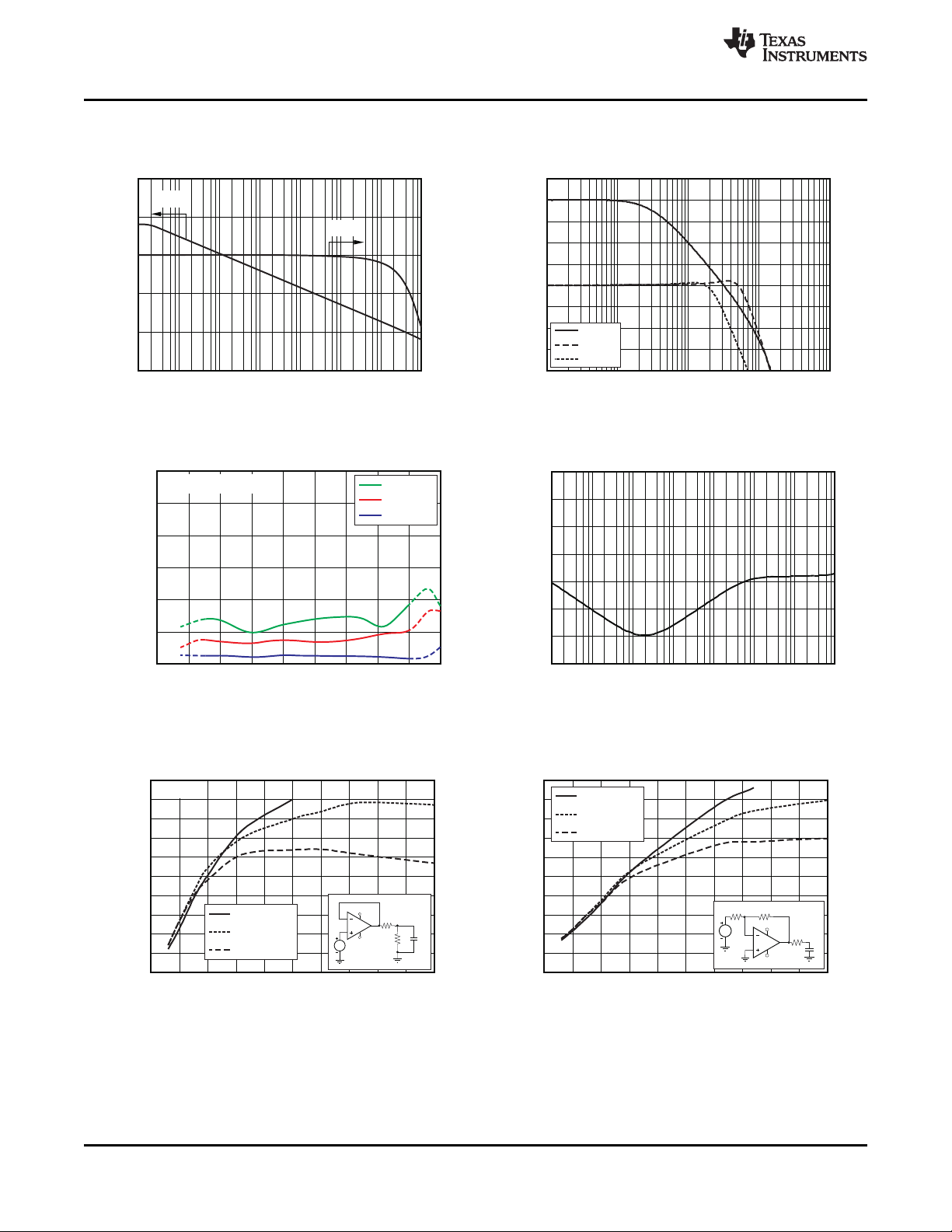
Open-Loop Gain and Phase vs Frequency Figure 19
Closed-Loop Gain vs Frequency Figure 20
Open-Loop Gain vs Temperature Figure 21
Open-Loop Output Impedance vs Frequency Figure 22
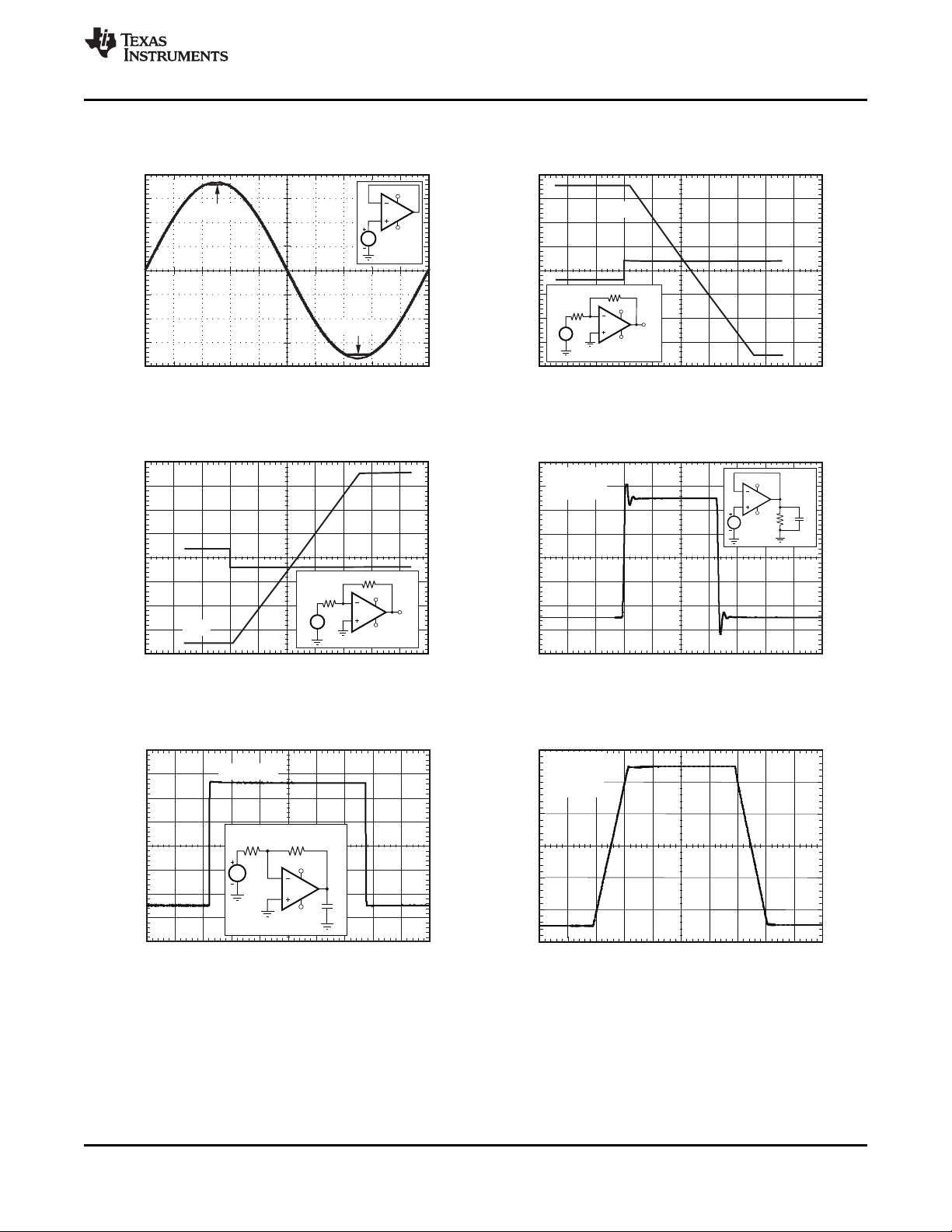
Small-Signal Overshoot vs Capacitive Load (100mV Output Step) Figure 23, Figure 24
No Phase Reversal Figure 25
Positive Overload Recovery Figure 26
Negative Overload Recovery Figure 27
Small-Signal Step Response (100mV) Figure 28, Figure 29
Large-Signal Step Response Figure 30, Figure 31
Large-Signal Settling Time (10V Positive Step) Figure 32
Large-Signal Settling Time (10V Negative Step) Figure 33
Short-Circuit Current vs Temperature Figure 34
Maximum Output Voltage vs Frequency Figure 35
Channel Separation vs Frequency Figure 36
www.ti.com
6 Submit Documentation Feedback Copyright © 2010–2012, Texas Instruments Incorporated
Product Folder Links: OPA171 OPA2171 OPA4171
10000
8000
6000
4000
2000
0
2000
4000
6000
8000
10000
-
-
-
-
-
V ( V)m
OS
15.5 16 16.5 17 17.5 18 18.5
V (V)
CM
10TypicalUnitsShown
Normal
Operation
V =+18.1V
CM
350
250
150
50
50
150
250
350
-
-
-
-
V ( V)m
OS
0 2 4 6 8 16 20
V (V)
SUPPLY
V = 1.35Vto 18V
10TypicalUnitsShown
±
SUPPLY
±
18141210
600
400
200
0
200
400
600
800
-
-
-
-
OffsetVoltage( V)m
-75 -50 -25 0 25 150
Temperature( C)°
50 12510075
5TypicalUnitsShown
1000
800
600
400
200
0
200
400
600
800
1000
-
-
-
-
-
V ( V)m
OS
-20 -15 -10 -5 0 5 10 15 20
V (V)
CM
V = 18.1V-
CM
10TypicalUnitsShown
-1200
-1100
-1000
-900
-800
-700
-600
-500
-400
-300
-100
0
100
200
300
400
500
600
700
800
900
1000
1200
OffsetVoltage( V)m
PercentageofAmplifiers(%)
16
14
12
10
8
6
4
2
0
-200
1100
DistributionTakenFrom3500Amplifiers
0
0.1
0.2
0.3
0.4
0.5
0.6
0.7
0.8
0.9
1.1
1.2
1.3
2
OffsetVoltageDrift( V/ C)m °
PercentageofAmplifiers(%)
25
20
15
10
5
0
1
DistributionTakenFrom110Amplifiers
1.5
1.7
1.9
1.8
1.6
1.4
www.ti.com
OPA2171
OPA4171
SBOS516D –SEPTEMBER 2010–REVISED SEPTEMBER 2012
TYPICAL CHARACTERISTICS
VS= ±18V, VCM= VS/2, R
OFFSET VOLTAGE PRODUCTION DISTRIBUTION OFFSET VOLTAGE DRIFT DISTRIBUTION
Figure 1. Figure 2.
= 10kΩ connected to VS/2, and CL= 100pF, unless otherwise noted.
LOAD
OPA171
OFFSET VOLTAGE vs TEMPERATURE OFFSET VOLTAGE vs COMMON-MODE VOLTAGE
Figure 3. Figure 4.
OFFSET VOLTAGE vs COMMON-MODE VOLTAGE
(Upper Stage) OFFSET VOLTAGE vs POWER SUPPLY
Copyright © 2010–2012, Texas Instruments Incorporated Submit Documentation Feedback 7
Figure 5. Figure 6.
Product Folder Links: OPA171 OPA2171 OPA4171
30
20
10
0
10
20
30
-
-
-
Common-ModeRejectionRatio( V/V)m
-75 -50 -25 0 25 150
Temperature( C)°
50 12510075
V =2.7V
S
V =4V
S
V =36V
S
3
2
1
0
1
2
3
-
-
-
Power-SupplyRejectionRatio( V/V)m
-75 -50 -25 0 25 150
Temperature( C)°
50 12510075
V =2.7Vto36V
S
V =4Vto36V
S
18
OutputVoltage(V)
0 2 4 6 8 16
OutputCurrent(mA)
10 12 14
17
16
15
14.5
-14.5
-15
-16
-17
-18
- °40 C
+25 C°
+85 C°
+125 C°
140
120
100
80
60
40
20
0
Common-ModeRejectionRatio(dB),
Power-SupplyRejectionRatio(dB)
1 10 100 1k 10k 10M
Frequency(Hz)
100k 1M
+PSRR
-PSRR
CMRR
15
14
13
12
11
10
9
8
7
6
5
4
3
2
1
0
I andI (pA)
B OS
-20 -12 -6 0 6 20
V (V)
CM
12
-I
B
+I
B
-I
OS
-18 18
V = 18.1V-
CM
V =16V
CM
I
B+
I
B-
I
OS
10000
1000
100
10
1
0
InputBiasCurrent(pA)
-75 -50 -25 0 25 150
Temperature( C)°
50 12510075
I
B
I
OS
OPA171
OPA2171
OPA4171
SBOS516D –SEPTEMBER 2010–REVISED SEPTEMBER 2012
TYPICAL CHARACTERISTICS (continued)
VS= ±18V, VCM= VS/2, R
IBAND IOSvs COMMON-MODE VOLTAGE INPUT BIAS CURRENT vs TEMPERATURE
OUTPUT VOLTAGE SWING vs OUTPUT CURRENT CMRR AND PSRR vs FREQUENCY
= 10kΩ connected to VS/2, and CL= 100pF, unless otherwise noted.
LOAD
Figure 7. Figure 8.
(Maximum Supply) (Referred-to Input)
www.ti.com
Figure 9. Figure 10.
CMRR vs TEMPERATURE PSRR vs TEMPERATURE
8 Submit Documentation Feedback Copyright © 2010–2012, Texas Instruments Incorporated
Figure 11. Figure 12.
Product Folder Links: OPA171 OPA2171 OPA4171
0.65
0.6
0.55
0.5
0.45
0.4
0.35
I (mA)
Q
-75 -50 -25 0 25 150
Temperature( C)°
1251007550
0.6
0.55
0.5
0.45
0.4
0.35
0.3
0.25
I (mA)
Q
0 4 8 12 16 36
SupplyVoltage(V)
32282420
SpecifiedSupply-VoltageRange
0.01
0.001
0.0001
0.00001
TotalHarmonicDistortion+Noise(%)
10 100 1k 10k 20k
Frequency(Hz)
TotalHarmonicDistortion+Noise(dB)
V =3V
BW=80kHz
OUT RMS
G=+1,R =10kW
L
G= 1,R =2k- W
L
-80
-100
-120
-140
0.1
0.01
0.001
0.0001
0.00001
TotalHarmonicDistortion+Noise(%)
0.01 0.1 1 10 20
OutputAmplitude(V )
RMS
-80
TotalHarmonicDistortion+Noise(dB)
BW=80kHz
G=+1,R =10kW
L
G= 1,R =2k- W
L
-100
-120
-140
1000
100
10
1
VoltageNoiseDensity(nV/ )Ö
Hz
1 10 100 1k 10k 1M
Frequency(Hz)
100k
1 V/divm
Time(1s/div)
www.ti.com
VS= ±18V, VCM= VS/2, R
THD+N RATIO vs FREQUENCY THD+N vs OUTPUT AMPLITUDE
SBOS516D –SEPTEMBER 2010–REVISED SEPTEMBER 2012
TYPICAL CHARACTERISTICS (continued)
= 10kΩ connected to VS/2, and CL= 100pF, unless otherwise noted.
LOAD
0.1Hz TO 10Hz NOISE FREQUENCY
Figure 13. Figure 14.
INPUT VOLTAGE NOISE SPECTRAL DENSITY vs
OPA171
OPA2171
OPA4171
QUIESCENT CURRENT vs TEMPERATURE QUIESCENT CURRENT vs SUPPLY VOLTAGE
Copyright © 2010–2012, Texas Instruments Incorporated Submit Documentation Feedback 9
Figure 15. Figure 16.
Figure 17. Figure 18.
Product Folder Links: OPA171 OPA2171 OPA4171
50
45
40
35
30
25
20
15
10
5
0
Overshoot(%)
0 100 200 300 400 500 600 700 800 900 1000
CapacitiveLoad(pF)
+18V
-18V
R
OUT
C
L
OPA171
R
L
G=+1
R =0W
OUT
R =25W
OUT
R =50W
OUT
R =10kW
L
50
45
40
35
30
25
20
15
10
5
0
Overshoot(%)
0 100 200 300 400 500 600 700 800 900 1000
CapacitiveLoad(pF)
OPA171
R =I10kW
R
OUT
C
L
RF=10kW
+18V
-18V
G= 1-
R =0W
OUT
R =25W
OUT
R =50W
OUT
3
2.5
2
1.5
1
0.5
0
A ( V/V)m
OL
-75 150
Temperature( C)°
-25-50 0
5TypicalUnitsShown
125100755025
V =2.7V
S
V =4V
S
V =36V
S
1M
100k
10k
1k
100
10
1
1m
Z ( )W
O
1 10 100 1k 10k 10M
Frequency(Hz)
100k 1M
180
135
90
45
0
45-
Gain(dB)
1 10 100 1k 10k 10M
Frequency(Hz)
1M100k
Phase
Gain
Phase( )°
180
135
90
45
0
-45
25
20
15
10
5
0
5
10
15
20
-
-
-
-
Gain(dB)
10k 100M
Frequency(Hz)
1M100k 10M
G=10
G=1
G= 1-
OPA171
OPA2171
OPA4171
SBOS516D –SEPTEMBER 2010–REVISED SEPTEMBER 2012
TYPICAL CHARACTERISTICS (continued)
VS= ±18V, VCM= VS/2, R
OPEN-LOOP GAIN AND PHASE vs FREQUENCY CLOSED-LOOP GAIN vs FREQUENCY
OPEN-LOOP GAIN vs TEMPERATURE OPEN-LOOP OUTPUT IMPEDANCE vs FREQUENCY
= 10kΩ connected to VS/2, and CL= 100pF, unless otherwise noted.
LOAD
Figure 19. Figure 20.
www.ti.com
Figure 21. Figure 22.
SMALL-SIGNAL OVERSHOOT vs CAPACITIVE LOAD SMALL-SIGNAL OVERSHOOT vs CAPACITIVE LOAD
(100mV Output Step) (100mV Output Step)
10 Submit Documentation Feedback Copyright © 2010–2012, Texas Instruments Incorporated
Figure 23. Figure 24.
Product Folder Links: OPA171 OPA2171 OPA4171
Time(20 s/div)m
20mV/div
+18V
-18V
R 2kW
F
=
R 2kW
I
=
C
L
OPA171
G= 1-
C =100pF
L
2V/div
Time(5 s/div)m
G=+1
R =10k
C =100pF
W
L
L
Time(5 s/div)m
5V/div
V
IN
V
OUT
2kW
20kW
V
IN
V
OUT
OPA171
G= 10-
+18V
-18V
20mV/div
Time(1 s/div)m
+18V
-18V
C
L
R
L
OPA171
G=+1
R =10k
C =100pF
W
L
L
Output
Output
Time(100 s/div)m
5V/div
+18V
-18V
37V
PP
SineWave
( 18.5V)±
OPA171
Time(5 s/div)m
5V/div
V
IN
V
OUT
2kW
20kW
V
IN
V
OUT
OPA171
G= 10-
+18V
-18V
www.ti.com
VS= ±18V, VCM= VS/2, R
NO PHASE REVERSAL POSITIVE OVERLOAD RECOVERY
NEGATIVE OVERLOAD RECOVERY (100mV)
SBOS516D –SEPTEMBER 2010–REVISED SEPTEMBER 2012
TYPICAL CHARACTERISTICS (continued)
= 10kΩ connected to VS/2, and CL= 100pF, unless otherwise noted.
LOAD
Figure 25. Figure 26.
SMALL-SIGNAL STEP RESPONSE
OPA171
OPA2171
OPA4171
Figure 27. Figure 28.
SMALL-SIGNAL STEP RESPONSE
(100mV) LARGE-SIGNAL STEP RESPONSE
Figure 29. Figure 30.
Copyright © 2010–2012, Texas Instruments Incorporated Submit Documentation Feedback 11
Product Folder Links: OPA171 OPA2171 OPA4171
 Loading...