

Texas Instruments OPA1632DRG4, OPA1632 Datasheet
SBOS286A − DECEMBER 2003 − REVISED SEPTEMBER 2006
Please be aware that an important notice concerning availability, standard warranty, and use in critical applications of Texas Instruments
High-Performance, Fully-Differential
AUDIO OP AMP
OPA1632
FEATURES
D SUPERIOR SOUND QUALITY
D ULTRA LOW DISTORTION: 0.000022%
D LOW NOISE: 1.3nV/√Hz
D HIGH SPEED:
− Slew Rate: 50V/µs
− Gain Bandwidth: 180MHz
D FULLY DIFFERENTIAL ARCHITECTURE:
− Balanced Input and Output Converts
Single-Ended Input to Balanced
Differential Output
D WIDE SUPPLY RANGE: ±2.5V to ±16V
D SHUTDOWN TO CONSERVE POWER
APPLICATIONS
D AUDIO ADC DRIVER
D BALANCED LINE DRIVER
D BALANCED RECEIVER
D ACTIVE FILTER
D PREAMPLIFIER
DESCRIPTION
The OPA1632 is a fully-differential amplifier designed
for driving high-performance audio analog-to-digital
converters (ADCs). It provides the highest audio quality ,
with very low noise and output drive characteristics
optimized for this application. The OPA1632’s excellent
gain bandwidth of 180MHz and very fast slew rate of
50V/µs produce exceptionally low distortion. Very low
input noise of 1.3nV/√Hz further ensures maximum
signal-to-noise ratio and dynamic range.
The flexibility of the fully differential architecture allows
for easy implementation of a single-ended to
fully-differential output conversion. Differential output
reduces even-order harmonics and minimizes
common-mode noise interference. The OPA1632
provides excellent performance when used to drive
high-performance audio ADCs such as the PCM1804.
A shutdown feature also enhances the flexibility of this
amplifier.
The OPA1632 is available in an SO-8 package and a
thermally-enhanced MSOP-8 PowerPAD package.
RELATED DEVICES
OPAx134 High-Performance Audio Amplifiers
OPA627/637 Precision High-Speed DiFET Amplifiers
OPAx227/x228 Low-Noise Bipolar Amplifiers
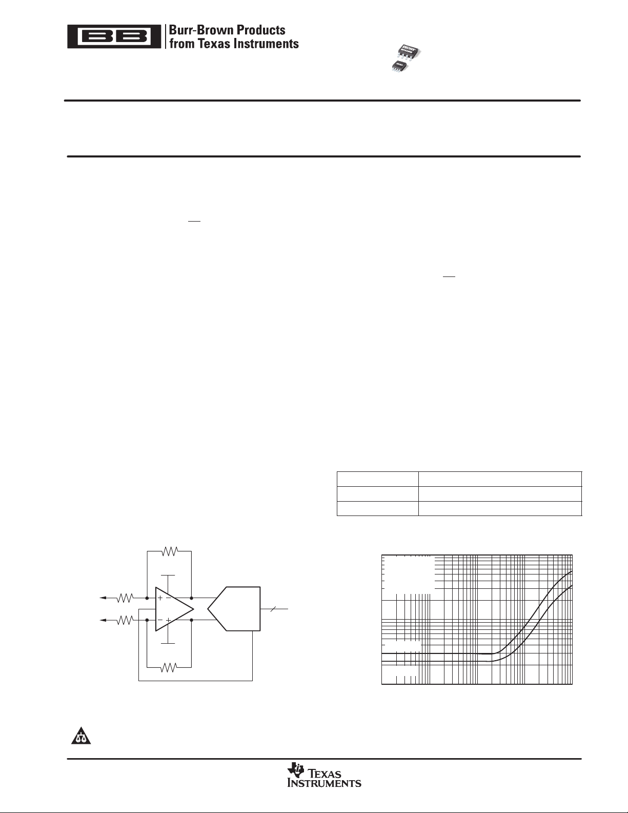
0.001
+15V
V
IN+
V
V
IN−
semiconductor products and disclaimers thereto appears at the end of this data sheet.
PowerPAD is a trademark of Texas Instruments. All other trademarks are the property of their respective owners.
! !
OCM
−
15V
Typical ADC Circuit
−
V
IN
V
+
IN
Digital
Output
V
COM
www.ti.com
0.0001
THD + Noise (%)
0.00001
Gain = +1
R
F
V
O
Differential I/O
RL=600
RL=2k
THD + NOISE vs FREQUENCY
Ω
= 348
=3Vrms
Ω
Ω
100010 100 10k 100k
Frequency (Hz)
Copyright 2003−2006, Texas Instruments Incorporated
"#$%
SO-8
D
−40°C to +85°C
OPA1632
OPA1632
MSOP-8
MSOP-8
DGN
−40°C to +85°C
1632
SBOS286A − DECEMBER 2003 − REVISED SEPTEMBER 2006
www.ti.com
PACKAGE/ORDERING INFORMATION
(1)
SPECIFIED
PRODUCT PACKAGE-LEAD
PACKAGE
DRAWING
TEMPERATURE
RANGE
PACKAGE
MARKING
ORDERING
NUMBER
TRANSPORT
MEDIA, QUANTITY
OPA1632D Rails, 100
OPA1632DR Tape and Reel, 2500
OPA1632DGN Rails, 100
PowerPAD
(1)
For the most current package and ordering information see the Package Option Addendum at the end of this document, or see the TI web site
OPA1632DGNR Tape and Reel, 2500
at www .ti.com.
ABSOLUTE MAXIMUM RATINGS
over operating free-air temperature range unless otherwise noted.
Supply Voltage, ±V
Input Voltage, V
Output Current, I
Differential Input Voltage, V
Maximum Junction Temperature, T
Operating Free-Air Temperature Range −40°C to +85°C. . . . . . . . . . . . . . .
Storage Temperature Range, T
ESD Ratings: Human Body Model 1kV. . . . . . . . . . . . . . . . . . . . . . . . . . . . . .
(1)
Stresses above these ratings may cause permanent damage.
S
. . . . . . . . . . . . . . . . . . . . . . . . . . . . . . . . . . . . . . . . . . . . .
I
O
Charge Device Model 500V. . . . . . . . . . . . . . . . . . . . . . . . . . .
Machine Model 200V. . . . . . . . . . . . . . . . . . . . . . . . . . . . . . . . .
ID
J
STG
(1)(2)
−65°C to +150°C. . . . . . . . . . . . . . . . .
±16.5V. . . . . . . . . . . . . . . . . . . . . . . . . . . . . . . . . . . . . . .
±V
S
150mA. . . . . . . . . . . . . . . . . . . . . . . . . . . . . . . . . . . . . . . .
±3V. . . . . . . . . . . . . . . . . . . . . . . . . . . . . . . . . .
150°C. . . . . . . . . . . . . . . . . . . . . . . . . .
proper handling and installation procedures can cause damage.
ESD damage can range from subtle performance degradation to
complete device failure. Precision integrated circuits may be more
susceptible t o damage because very small parametric changes could
cause the device not to meet its published specifications.
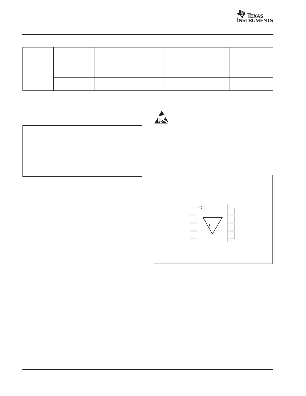
PIN CONFIGURATION
Top View MSOP, SO
This integrated circuit can be damaged by ESD. Texas
Instruments recommends that all integrated circuits be
handled with appropriate precautions. Failure to observe
Exposure to absolute maximum conditions for extended periods
may degrade device reliability. These are stress ratings only , an d
functional operation of the device at these or any other conditions
beyond those specified is not implied.
(2)
The OPA1632 MSOP-8 package version incorporates a
PowerPAD on the underside of the chip. This acts as a heatsink
and must be connected to a thermally dissipative plane for proper
power dissipation. Failure to do so may result in exceeding the
maximum junction temperature, which can permanently damage
the device. See TI technical brief SLMA002 for more information
about using the PowerPAD thermally enhanced package.
V
V
V
OCM
V+
OUT+
−
IN
OPA1632
1
2
3
4
V
8
IN+
Enable
7
−
V
6
V
5
OUT−
2
"#$%
www.ti.com
SBOS286A − DECEMBER 2003 − REVISED SEPTEMBER 2006
ELECTRICAL CHARACTERISTICS: VS = ±15V
VS = ±15V: RF = 390Ω, RL = 800Ω, and G = +1, unless otherwise noted.
PARAMETER CONDITIONS MIN TYP MAX UNITS
OFFSET VOLTAGE
Input Offset Voltage ±0.5 ±3 mV
vs Temperature dVos/dT ±5 µV/_C
vs Power Supply, DC PSRR 316 13 µV/V
INPUT BIAS CURRENT
Input Bias Current I
Input Offset Current I
NOISE
Input Voltage Noise f = 10 kHz 1.3 nV/√Hz
Input Current Noise f = 10 kHz 0.4 pA/√Hz
INPUT VOLTAGE
Common-Mode Input Range (V−) + 1.5 (V+) − 1 V
Common-Mode Rejection Ratio, DC 74 90 dB
INPUT IMPEDANCE
Input Impedance (each input pin) 34 || 4 MΩ || pF
OPEN-LOOP GAIN
Open-Loop Gain , DC 66 78 dB
FREQUENCY RESPONSE
Small-Signal Bandwidth G = +1, RF= 348Ω 180 MHz
(VO = 100mVPP, Peaking < 0.5 dB) G = +2, RF = 602Ω 90 MHz
Bandwidth for 0.1dB Flatness G = +1, VO = 100mV
Peaking at a Gain of 1 VO = 100mV
Large-Signal Bandwidth G = +2, VO = 20V
Slew Rate (25% to 75% ) G = +1 50 V/µs
Rise and Fall Time G = +1, VO = 5V Step 100 ns
Settling Time to 0.1% G = +1, VO = 2V Step 75 ns
0.01% G = +1, VO = 2V Step 200 ns
Total Harmonic Distortion + Noise G = +1, f = 1kHz, VO = 3Vrms
Differential Input/Output RL = 600Ω 0.0003 %
Differential Input/Output RL = 2kΩ 0.000022 %
Single-Ended In/Differential Out RL = 600Ω 0.000059 %
Single-Ended In/Differential Out RL = 2kΩ 0.000043 %
Intermodulation Distortion G = +1, SMPTE/DIN, VO = 2V
Differential Input/Output RL = 600Ω 0.00008 %
Differential Input/Output RL = 2kΩ 0.00005 %
Single-Ended In/Differential Out RL = 600Ω 0.0001 %
Single-Ended In/Differential Out RL = 2kΩ 0.0007 %
Headroom THD < 0.01%, RL = 2kΩ 20.0 V
OUTPUT
Voltage Output Swing RL = 2kΩ (V+) − 1.9 (V−) + 1.9 V
Short-Circuit Current I
Closed-Loop Output Impedance G = +1, f = 100kHz 0.3 Ω
POWER-DOWN
Enable Voltage Threshold (V−) + 2 V
Disable Voltage Threshold (V−) + 0.8 V
Shutdown Current V
Turn-On Delay Time for IQ to Reach 50% 2 µs
Turn-Off Delay Time for IQ to Reach 50% 2 µs
POWER SUPPL Y
Specified Operating Voltage ±15 ±16 V
Operating Voltage ±2.5 V
Quiescent Current I
TEMPERATURE RANGE
Specified Range −40 +85 _C
Operating Range −40 +125 _C
Storage Range −65 +150 _C
Thermal Resistance
(1)
Amplifier has internal 50kΩ pull-up resistor to V
(1)
OS
SC
B
G = +5, RF = 1.5kΩ 36 MHz
G = +10, RF = 3.01kΩ 18 MHz
PP
PP
PP
PP
RL = 800Ω (V+) − 4.5 (V−) + 4.5 V
Sourcing/Sinking +50/−60 85 mA
= −15V 0.85 1.5 mA
ENABLE
Q
q
JA
pin. This enables the amplifier with no connection to shutdown pin.
CC+
Per Channel 14 17.1 mA
OPA1632
2 6 µA
±100 ±500 nA
40 MHz
0.5 dB
800 kHz
PP
200 _C/W
3
"#$%
SBOS286A − DECEMBER 2003 − REVISED SEPTEMBER 2006
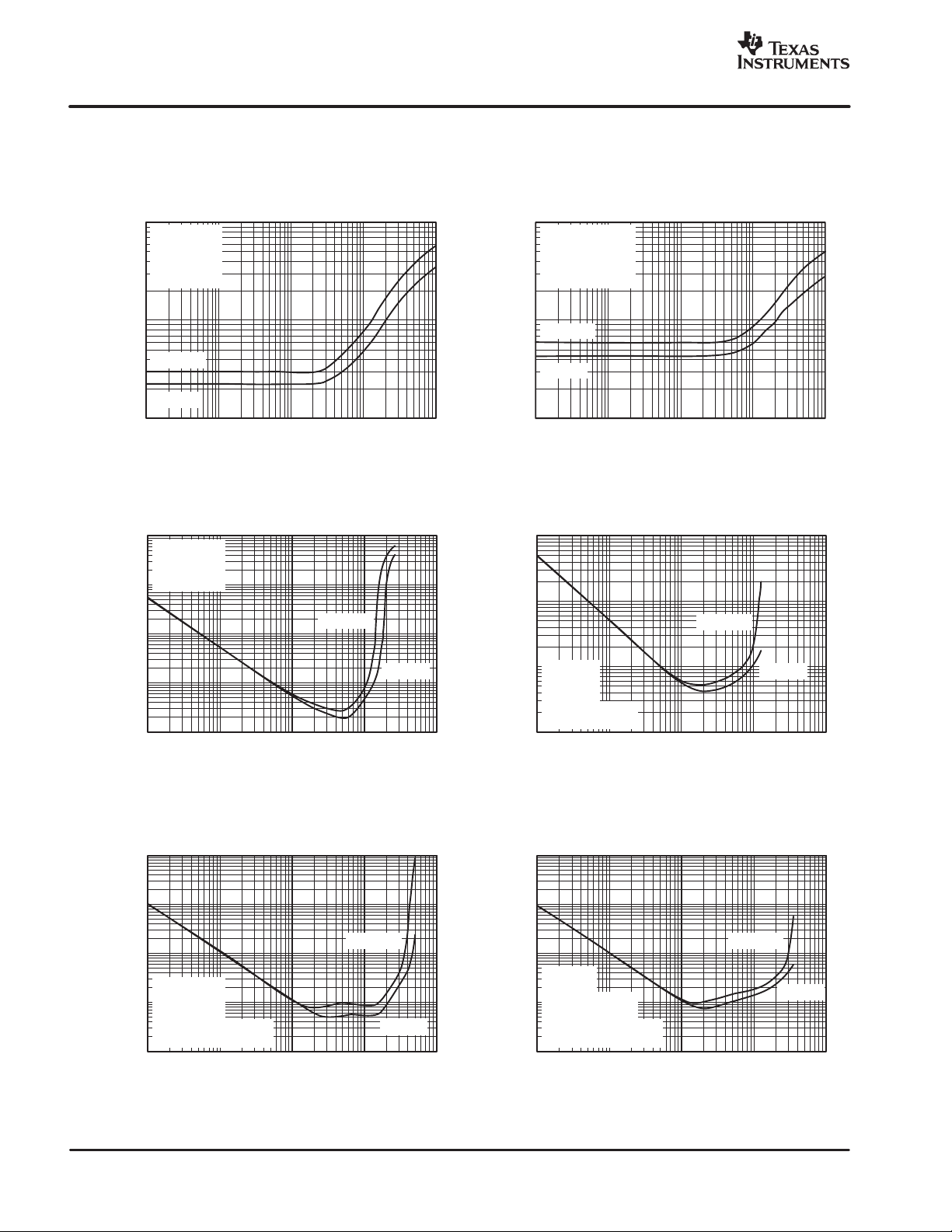
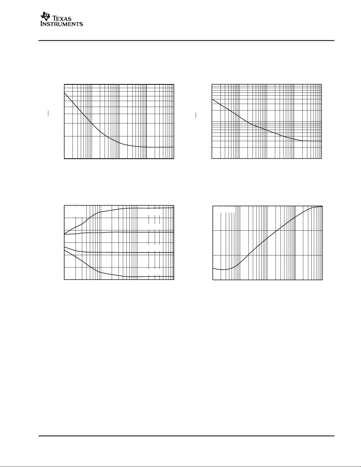
TYPICAL CHARACTERISTICS
At TA = +25°C, VS = ±15V, and RL = 2kΩ, unless otherwise noted.
www.ti.com
0.001
Gain= +1
= 348
R
F
=3Vrms
V
O
Differential I/O
0.0001
THD + Noise (%)
0.00001
RL=600
RL=2k
10 100 1k 10k 100k
0.1
Gain = +1
R
F
f=1kHz
0.01
Differential I/O
0.001
THD + NOISE vs FREQUENCY
Ω
Ω
Ω
Frequency (Hz)
THD + NOISE vs OUTPUT VOLTAGE
Ω
=348
RL= 600
0.001
Gain = +1
RF=348
VO=3Vrms
Single−Ended Input
Differential Output
0.0001
THD + Noise (%)
0.00001
Ω
RL=600
RL=2k
10 100 1k 10k 100k
0.01
0.001
THD + NOISE vs FREQUENCY
Ω
Ω
Ω
Frequency (Hz)
THD + NOISE vs OUTPUT VOLTAGE
RL= 600
Ω
THD + Noise (%)
0.0001
0.00001
0.01 0.1 1 10 100
Differential Output Voltage (Vrms)
INTERMODULATION DISTORTION
0.1
0.01
0.001
IMD(%)
0.0001
0.00001
Gain = +1
=348
R
F
Differential I/O
SMPTE 4:1; 60Hz, 7kHz
DIN 4:1; 250Hz, 8kHz
0.01 0.1 1 10 100
vs OUTPUT VOLTAGE
Ω
Differential Output Voltage (V
RL=600
PP
)
RL=2k
Ω
RL=2k
Ω
Ω
0.0001
THD + Noise (%)
0.00001
IMD(%)
0.0001
0.00001
Gain = +1
Ω
=348
R
F
f=1kHz
Single−Ended Input
Differential Output
0.01 0.1 1 10 100
Differential Output Voltage (Vrms)
INTERMODULATION DISTORTION
0.1
0.01
0.001
Gain = +1
=348
R
F
Single−Ended Input
Differential Output
SMPTE 4:1; 60Hz, 7kHz
DIN 4:1; 250Hz, 8kHz
0.01 0.1 1 10 100
vs OUTPUT VOLTAGE
Ω
Differential Output Voltage (V
RL= 600
)
PP
RL=2k
Ω
RL=2k
Ω
Ω
4
www.ti.com
TYPICAL CHARACTERISTICS (Cont.)
At TA = +25°C, VS = ±15V, and RL = 2kΩ, unless otherwise noted.
"#$%
SBOS286A − DECEMBER 2003 − REVISED SEPTEMBER 2006
10
Hz)
√
(nV/
n
V
1
10 100 1k 10k 100k
15
RF=1k
G=+2
10
5
(V)
0
O
V
−
5
−
10
−
15
100 1k 10k 100k
VOLTAGE NOISE vs FREQUENCY
Frequency (Hz)
vs DIFFERENTIAL LOAD RESISTANCE
Ω
OUTPUT VOLTAGE
(Ω)
R
L
VCC=±15V
VCC=±5V
VCC=±5V
VCC=±15V
10
Hz)
√
1
(pA/
n
I
0.1
10 100 1k 10k 100k
100
VCC=±5V
)
Ω
10
1
Output Impedance (
0.1
100k 1M 10M 100M 1G
CURRENT NOISE vs FREQUENCY
Frequency (Hz)
OUTPUT IMPEDANCE
vs FREQUENCY
Frequency (Hz)
5
 Loading...