

Page 1

www.ti.com
查询ONET4291VA供应商
1 GBPS TO 4.25 GBPS MULTI-RATE VCSEL DRIVER
ONET4291VA
SLLS674 – SEPTEMBER 2005
FEATURES
• Operating Temperature –40 ° C to 85 ° C
• Multi-Rate Operation from 1 Gbps Up • Small Footprint Surface Mount 4 mm × 4 mm,
To 4.25 Gbps 20-Pin QFN Package
• 2-Wire Digital Interface
• Digitally Selectable Modulation Current
• Digitally Selectable Bias Current
• Automatic Power Control (APC) Loop
• Supports Transceiver Management
APPLICATIONS
• Multirate SFP/SFF Modules
• 1.0625 Gbps, 2.125 Gbps, and 4.25 Gbps Fibre
Channel Transmitters
• Gigabit Ethernet Transmitters
System (TMS)
• Includes Laser Safety Features
• Analog Temperature Sensor Output
• Single 3.3-V Supply
DESCRIPTION
The ONET4291VA is a versatile high-speed multi-rate VCSEL driver for fiber optic applications with data rates up
to 4.25 Gbps.
The device provides a 2-wire interface which allows digital control of the modulation and bias currents,
eliminating the need for of external components.
The ONET4291VA includes an integrated automatic power control loop as well as circuitry to support laser safety
and transceiver management systems.
The part is available in a small footprint 4 mm × 4 mm 20-pin QFN package and it requires a single 3.3-V supply.
This power efficient multi-rate VCSEL driver is characterized for operation from –40 ° C to 85 ° C ambient
temperature.
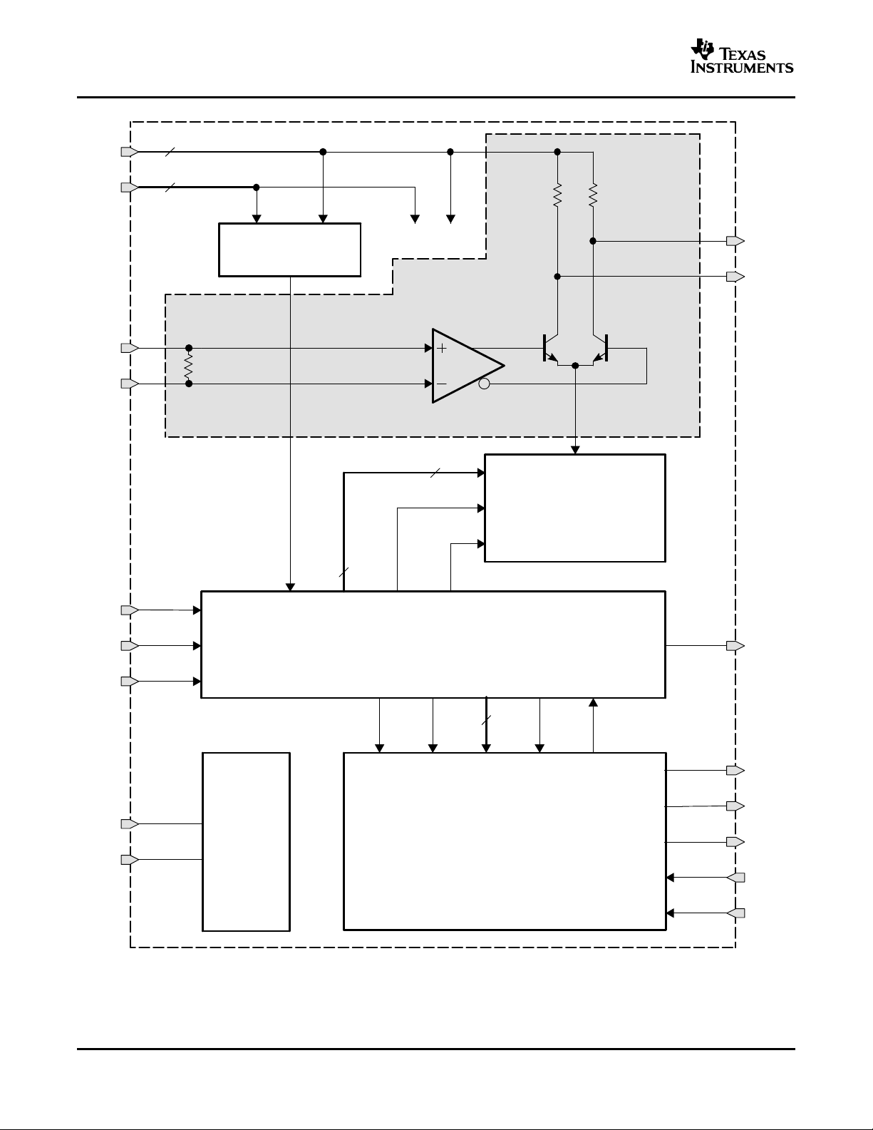
BLOCK DIAGRAM
A simplified block diagram of the ONET4291VA is shown in Figure 1 .
This compact, low power 1-Gbps to 4.25-Gbps multi-rate VCSEL driver consists of a high-speed current
modulator, a modulation current generator, power-on reset circuitry, a 2-wire interface and control logic block, a
bias current generator and automatic power control loop, and an analog reference block.
Please be aware that an important notice concerning availability, standard warranty, and use in critical applications of Texas
Instruments semiconductor products and disclaimers thereto appears at the end of this data sheet.
PRODUCTION DATA information is current as of publication date.
Products conform to specifications per the terms of the Texas
Instruments standard warranty. Production processing does not
necessarily include testing of all parameters.
Copyright © 2005, Texas Instruments Incorporated
Page 2
www.ti.com
DIN+
DIN−
Limiting
Gain Stage
GND
DOUT+
DOUT−
Power-On Reset
GND VCC
RESET
RESET
Modulation
Current
Generator
MODC
IMOD
MODR
ENA
MODC MODR ENA
FLT
VCC
SCK
SDA
DIS
SCK
SDA
DIS
FLT
Bias Current Generator
and Automatic Power
Control Loop (APC)
BIAS
MONB
MONP
BIAS
MONB
MONP
MD
COMP
MD
COMP
RZTC
TS
RZTC
TS
2-Wire Interface and Control Logic Clock
FAULTPDPBIASCOLEENA
High-Speed Current Modulator
3
2
100 Ω
8
8
60 Ω60 Ω
8
FAULTPDPBIASCOLEENA
Analog Reference
B0072-01
ONET4291VA
SLLS674 – SEPTEMBER 2005
2
Figure 1. Simplified Block Diagram of the ONET4291VA
Page 3

www.ti.com
ONET4291VA
SLLS674 – SEPTEMBER 2005
HIGH-SPEED CURRENT MODULATOR
The data signal is applied to the high-speed current modulator by means of the input signal pins DIN+/DIN–,
which provide on-chip differential 100- Ω line-termination. The succeeding limiting gain stage ensures sufficient
drive amplitude and edge-speed for driving the current modulator differential pair.
The modulation current is sunk from the common emitter node of the differential pair by means of a modulation
current generator, which is digitally controlled by the 2-wire interface and control logic block.
The collector nodes of the differential pair are connected to the output pins DOUT+/DOUT–, which include
on-chip 2 × 60- Ω back-termination to VCC. The 60- Ω back-termination helps to sufficiently suppress signal
distortion caused by double reflections for VCSEL diodes with impedances ranging from 50 Ω through 75 Ω .
MODULATION CURRENT GENERATOR
The modulation current generator provides the current for the current modulator described above. The circuit is
digitally controlled by the 2-wire interface and control logic block.
An 8-bit wide control bus, MODC, is used to set the desired modulation current.
Furthermore, two modulation current ranges are selected by means of the MODR signal.
The ENA signal enables or disables the modulation current generator.
The modulation current can be disabled by setting the DIS input pin to a high level. The modulation current is
also disabled in a fault condition if the fault detection enable register flag FLTEN is set.
For more information about the register functionality, see the register mapping description.
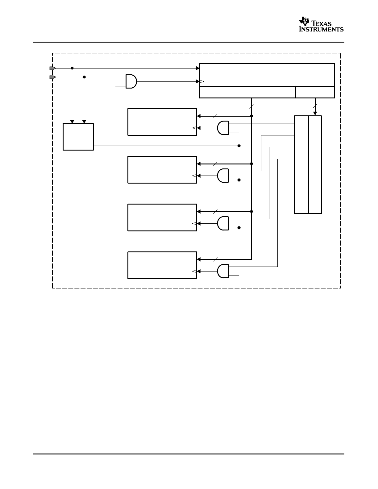
2-WIRE SERIAL INTERFACE AND CONTROL LOGIC
The ONET4291VA uses a 2-wire serial interface for digital control. A simplified block diagram of this interface is
shown in Figure 2 .
The two circuit inputs, SDA and SCK, are driven, respectively, by the serial data and serial clock from a
microprocessor, for example. Both inputs include 100-k Ω pullup resistors to VCC. For driving these inputs, an
open drain output is recommended.
A write cycle consists of a START command, three address bits with MSB first, eight data bits with MSB first,
and a STOP command. In idle mode, both SDA and SCK lines are at a high level.
A START command is initiated by the falling edge of SDA with SCK at a high level, transitioning to a low level.
Bits are clocked into an 11-bit wide shift register during the high level of the system clock SCK.
A STOP command is detected on the rising edge of SDA after SCK has changed from a low to a high level.
At the time of detection of a STOP command, the eight data bits from the shift register are copied to a selected
8-bit register. Register selection occurs according to the three address bits in the shift register, which are
decoded to eight independent select signals using a 3 to 8 decoder block.
In the ONET4291VA, only addresses 0 (000b) through 3 (011b) are used.
3
Page 4
www.ti.com
Start/Stop
Detector
Logic
111
110
101
100
011
010
001
000
START
STOP
SDA
SCK
8 Bit Register
Control Functions (6 Bit)
Unused (2 Bit)
8
8
8 Bit Register
Modulation Current (8 Bit)
8
11 Bit Shift Register
8 Bits Data 3 Bits Addr
3 to 8 Decoder
3
B0068-02
8 Bit Register
Bias Current (8 Bit)
8
8 Bit Register
Unused (8 Bit)
8
ONET4291VA
SLLS674 – SEPTEMBER 2005
Figure 2. Simplified 2-Wire Interface Block Diagram
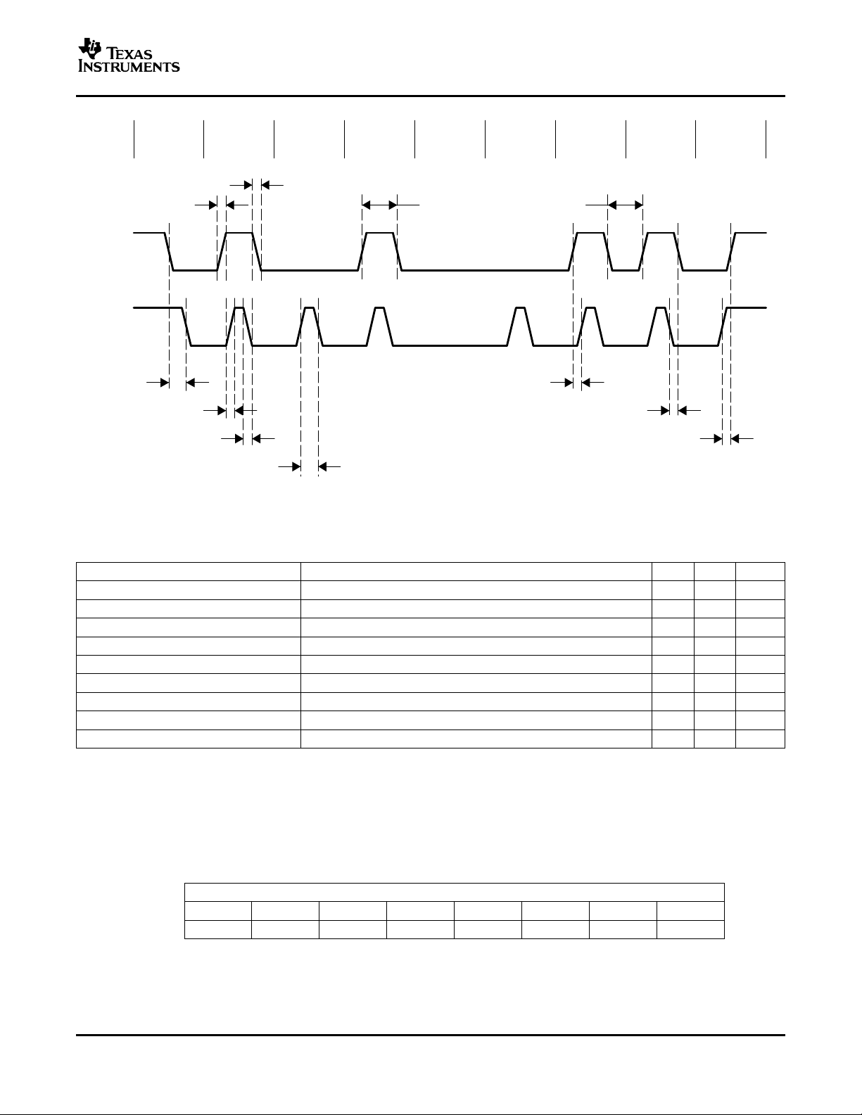
The timing definition for the serial data signal SDA and the serial clock signal SCK is shown in Figure 3 .
The corresponding timing requirements are listed in Table 1 .
4
Page 5
www.ti.com
START STOP1 0 1 0 1 1
SDA
SCK
DTA
R
DTA
F
STRT
HLD
CLK
R
CLK
F
CLK
HI
DTA
HI
DTA
STP
DTA
WT
DTA
HLD
STOP
STP
T0077-01
ONET4291VA
SLLS674 – SEPTEMBER 2005
Figure 3. 2-Wire Interface Timing Diagram
Table 1. 2-Wire Interface Timing
PARAMETER DESCRIPTION MIN MAX UNIT
STRT
HLD
CLK
, DTA
R
CLK
, DTA
F
CLK
HI
DTA
HI
DTA
STP
DTA
WT
DTA
HLD
STOP
STP
REGISTER MAPPING
The register mapping for the register addresses 0 (000b) through 3 (011b) are shown in Table 2 to Table 5 .
Register 3 is included for future enhancements. It is not used in the current device.
Table 6 describes the circuit functionality based on the register settings.
START hold time Time required from data falling edge to clock falling edge at START 10 ns
Clock and data rise time Clock and data rise time 10 ns
R
Clock and data fall time Clock and data fall time 10 ns
F
Clock high time Minimum clock high period 50 ns
Data high time Minimum data high period 100 ns
Data setup time Minimum time from data rising edge to clock rising edge 10 ns
Data wait time Minimum time from data falling edge to data rising edge 50 ns
Data hold time Minimum time from clock falling edge to data falling edge 10 ns
STOP setup time Minimum time from clock rising edge to data rising edge at STOP 10 ns
Table 2. Register 0 (000b) Mapping
address 0 (000b)
bit 7 bit 6 bit 5 bit 4 bit 3 bit 2 bit 1 bit 0
ENA PDP PDR OLE FLTEN MODR – –
5
Page 6
www.ti.com
ONET4291VA
SLLS674 – SEPTEMBER 2005
Table 3. Register 1 (001b) Mapping
address 1 (001b)
bit 7 bit 6 bit 5 bit 4 bit 3 bit 2 bit 1 bit 0
MODC7 MODC6 MODC5 MODC4 MODC3 MODC2 MODC1 MODC0
Table 4. Register 2 (010b) Mapping
address 2 (010b)
bit 7 bit 6 bit 5 bit 4 bit 3 bit 2 bit 1 bit 0
BIASC7 BIASC6 BIASC5 BIASC4 BIASC3 BIASC2 BIASC1 BIASC0
Table 5. Register 3 (011b) Mapping
address 3 (011b)
bit 7 bit 6 bit 5 bit 4 bit 3 bit 2 bit 1 bit 0
– – – – – – – –
Table 6. Register Functionality
Symbol Register Function
ENA Enable Enables chip when set to 1. Can be toggled to reset a fault condition.
PDP Photodiode polarity Photodiode polarity bit:
PDR Photodiode current range Photodiode current range bit:
OLE Open loop enable Open loop enable bit:
FLTEN Fault detection enable Fault detection enable bit:
MODR Modulation current range Laser modulation current range:
MODC7 Modulation current bit 7 (MSB) Modulation current setting:
MODC6 Modulation current bit 6
MODC5 Modulation current bit 5 MODR = 1 (see above):
MODC4 Modulation current bit 4 Modulation current: 100 µ A – 15.4 mA with 68 µ A step size
MODC3 Modulation current bit 3
MODC2 Modulation current bit 2 MODR = 0 (see above):
MODC1 Modulation current bit 1 Modulation current: 100 µ A – 12 mA with 51 µ A step size
MODC0 Modulation current bit 0 (LSB)
BIASC7 Bias current bit 7 (MSB) closed loop (APC):
BIASC6 Bias current bit 6 Coupling ratio CR between VCSEL bias current and photodiode current is:
BIASC5 Bias current bit 5 CR = I
BIASC4 Bias current bit 4 PDR = 0 (see above), BIASC = 0 .. 255, I
BIASC3 Bias current bit 3 I
BIASC2 Bias current bit 2 PDR = 1 (see above), BIASC = 0 .. 255, I
BIASC1 Bias current bit 1 I
BIASC0 Bias current bit 0 (LSB) open loop: I
1 = common anode
0 = common cathode
1 = 0 µ A – 500 µ A with 2- µ A resolution
0 = 0 µ A – 250 µ A with 1- µ A resolution
1 = open loop bias current control
0 = closed loop bias current control
1 = fault detection on
0 = fault detection off
1 = 0 mA – 15 mA
0 = 0 mA – 12 mA
BIAS-VCSEL
BIAS-VCSEL
BIAS-VCSEL
/ I
PD
= 100 µ A + (1 µ A × CR × BIASC)
= 100 µ A + (2 µ A × CR × BIASC)
BIAS-VCSEL
= 100 µ A + (47 µ A × BIASC)
BIAS-VCSEL
BIAS-VCSEL
≤ 12 mA:
≤ 12 mA:
6
Page 7

www.ti.com
ONET4291VA
SLLS674 – SEPTEMBER 2005
BIAS CURRENT GENERATION AND APC LOOP
The bias current generation and APC loop are controlled by means of the 2-wire interface.
In open loop operation, selected by setting OLE = 1 (bit 4 of register 0), the bias current is set directly by the 8-bit
wide control word BIASC[0..7] (register 2).
In automatic power control mode, selected by setting OLE = 0, the bias current depends on the register settings
BIASC[0..7] and the coupling ratio (CR) between the VCSEL bias current and the photodiode current.
CR = I
BIAS-VCSEL
Two photodiode current ranges can be selected by means of the PDR register (bit 5 of register 0). The
photodiode range should be chosen to keep the laser bias control DAC close to the center of its range. This
keeps the laser bias current setpoint resolution high and the loop settling time constant within specification.
For details regarding the bias current setting in open loop as well as in closed loop mode, see Table 6 .
In closed loop mode, the photodiode polarity bit, PDP, must be set for common anode or common cathode
configuration to ensure proper operation. In open loop mode if a photodiode is still present, the photodiode
polarity bit must be set to the opposite setting.
ANALOG REFERENCE
The ONET4291VA is supplied by a single 3.3-V ±10% supply voltage connected to the VCC pins. This voltage is
referenced to ground (GND).
On-chip bandgap voltage circuitry generates a reference voltage, independent of the supply voltage, from which
all other internally required voltages and bias currents are derived.
An external zero temperature coefficient resistor must be connected from the RZTC pin of the device to ground
(GND). This resistor is used to generate a precise zero TC current which is used as a reference current for the
on-chip DACs.
In order to minimize the module component count, the ONET4291VA VCSEL driver provides an on-chip
temperature sensor. The output voltage of the temperature sensor is available at the TS pin.
The voltage is V
Note that the voltage at TS is not buffered. As a result, TS can only drive capacitive loads.
/ IPD.
= 9.4 mV × TEMP + 1337 mV with TEMP given in ° C.
TS
POWER-ON RESET AND REGISTER LOADING SEQUENCE
The ONET4291VA has power on reset circuitry which ensures that all registers are reset to zero during startup.
After the power-on to initialize time (T
), the internal registers are ready to be loaded. It is important that the
INIT1
registers are loaded in the following order:
1. Bias current register (register 2, 010b),
2. Modulation current register (register 1, 001b),
3. Control register (register 0, 000b).
The part will be ready to transmit data after the initialize to transmit time T
, assuming that the control register
INIT2
enable bit ENA is 1 and the disable pin DIS is low.
The ONET4291VA can be disabled using either the ENA control register bit or the disable pin DIS. In both cases
the internal registers are not reset. After the disable pin DIS is de-asserted and/or the enable bit ENA is
re-asserted the part returns to its prior output settings.
LASER SAFETY FEATURES AND FAULT RECOVERY PROCEDURE
The ONET4291VA provides built in laser safety features. The following fault conditions are detected:
1. Voltage at MONB exceeds 1.2 V,
2. Photodiode current exceeds 150% of its target value,
3. Bias control DAC drops in value by more than 33% in one step.
If one or more fault conditions occur and the fault enable bit FLTEN is set to 1, the ONET4192VA responds by:
1. Setting the VCSEL bias current to zero.
7
Page 8

www.ti.com
GND
MOD
MOD+
GND
BIAS
DIS
RZTC
TS
SCK
SDA
VCC
DIN+
DIN−
VCC
FLT
RGP PACKAGE
(TOP VIEW)
2019181716
6
7
8
9
10
PD
VCC
CAPC
MONP
MONB
P0031-01
15
14
13
12
11
1
2
3
4
5
EP
ONET4291VA
SLLS674 – SEPTEMBER 2005
2. Setting the modulation current to zero.
3. Asserting and latching the FLT pin.
Fault recovery is performed by the following procedure:
1. The disable pin DIS and/or the enable control bit ENA are toggled for at least the fault latch reset time
T
.
RESET
2. The FLT pin de-asserts while the disable pin DIS is asserted or the enable bit ENA is de-asserted.
3. If the fault condition is no longer present, the part will return to normal operation with its prior output settings
after the disable negate time T
4. If the fault condition is still present, FLT re-asserts once DIS is set to low level and the part will not return to
normal operation.
PACKAGE
For the ONET4291VA, a small footprint 4 mm × 4 mm 20-pin QFN package with a lead pitch of 0,5 mm is used.
The pin out is shown in Figure 4 .
.
ON
Figure 4. Pinout of ONET4291VA in a 4 mm × 4 mm 20-Pin QFN Package
TERMINAL FUNCTIONS
TERMINAL
NO. NAME
1 DIS CMOS-in Disables both bias and modulation current when set to high state. Toggle to reset a fault
2 RZTC Analog Connect external zero TC 30-k Ω to ground (GND). Used to generate a defined zero TC reference
3 TS Analog-out Temperature sensor output. Not buffered, capacitive load only.
4 SCK CMOS-in 2-wire interface serial clock. Includes a 100-k Ω pullup resistor to VCC.
5 SDA CMOS-in 2-wire interface serial data input. Includes a 100-k Ω pullup resistor to VCC.
6, 9, 14 VCC Supply 3.3-V ± 10% supply voltage
7 DIN+ Analog-in Non-inverted data input. On-chip differentially 100- Ω terminated to DIN–. Must be ac coupled.
8 DIN– Analog-in Inverted data input. On-chip differentially 100- Ω terminated to DIN+. Must be ac coupled.
10 FLT CMOS-out Fault detection flag
11 MONB Analog-out Bias current monitor. Sources an 8.3% replica of the bias current. Connect an external resistor to
8
TYPE DESCRIPTION
condition
current for internal DACs.
ground (GND). If the voltage at this pin exceeds 1.2 V a fault is triggered.
Page 9

www.ti.com
ONET4291VA
SLLS674 – SEPTEMBER 2005
TERMINAL FUNCTIONS (continued)
TERMINAL
NO. NAME
12 MONP Analog-out Photodiode current monitor. Sources a 50% replica of the photodiode current. Connect an
13 CAPC Analog Compensation pin used to control the bandwidth of the APC loop. Connect a 0.01- µ F capacitor to
15 PD Analog Monitor photodiode input. The pin can source or sink current dependent on PDP register setting.
16 BIAS Analog VCSEL diode bias current source. Connect to laser anode through inductor. Murata
17, 20, EP GND Supply Circuit ground. The exposed die pad (EP) must be grounded.
18 MOD+ CML-out Non-inverted modulation current output. AC coupled to anode of common cathode VCSEL.
19 MOD– CML-out Inverted modulation current output. AC coupled through VCSEL matching resistor to ground
TYPE DESCRIPTION
external resistor to ground (GND).
ground.
Pin supplies >1.5-V reverse bias.
BLM15HG102SN1 is recommended.
On-chip 60- Ω back-terminated to VCC.
(GND). On-chip 60- Ω back-terminated to VCC.
ABSOLUTE MAXIMUM RATINGS
(1)
over operating free-air temperature range (unless otherwise noted)
VALUE / UNIT
V
V
V
VPD, V
CC
, V
DIS
DIN–
, VTS, V
RZTC
, V
, V
FLT
MONB,
, V
BIAS
MOD+
, V
MOD–
, V
SDA
, V
MONP
CAPC
SCK
V
, V
Supply voltage –0.3 V to 4 V
, Voltage at DIS, RZTC, TS, SCK, SDA, DIN+, DIN–, FLT, MONB, MONP, –0.3 V to 4 V
DIN+
, CAPC, PD, BIAS, MOD+, MOD–
(2)
ESD ESD rating at all pins 3 kV (HBM)
T
J,max
T
STG
T
A
T
LEAD
Maximum junction temperature 125 ° C
Storage temperature range –65 ° C to 85 ° C
Characterized free-air operating temperature range –40 ° C to 85 ° C
Lead temperature 1,6 mm (1/16 inch) from case for 10 seconds 260 ° C
(1) Stresses beyond those listed under absolute maximum ratings may cause permanent damage to the device. These are stress ratings
only, and functional operation of the device at these or any other conditions beyond those indicated under recommended operating
conditions is not implied. Exposure to absolute–maximum–rated conditions for extended periods may affect device reliability.
(2) All voltage values are with respect to network ground terminal.
RECOMMENDED OPERATING CONDITIONS
PARAMETER CONDITIONS MIN TYP MAX UNIT
V
V
V
R
V
t
t
T
(1) Changing the value alters DAC ranges.
Supply voltage 2.9 3.3 3.6 V
CC
CMOS input high voltage DIS, SCK, SDA 2 V
IH
CMOS input low voltage DIS, SCK, SDA 0.8 V
IL
Bias output headroom voltage VCC– V
Photodiode current range µ A
Zero TC resistor value
RZTC
Differential input voltage swing 200 800 2400 mVp-p
IN
Input rise time ps
R-IN
Input fall time ps
F-IN
Operating free-air temperature –40 85 ° C
A
(1)
Control bit PDR = 1, step size = 2 µ A 10 500
Control bit PDR = 0, step size = 1 µ A 5 250
1.22-V bias across resistor 29.7 30 30.3 k Ω
20%–80%, f
20%–80%, f
20%–80%, f
20%–80%, f
, I
BIAS
= 10 mA 500 mV
BIAS
= 1.25 Gbps 160
BIT
≥ 2.125 Gbps 100
BIT
= 1.25 Gbps 160
BIT
≥ 2.125 Gbps 100
BIT
9
Page 10

www.ti.com
ONET4291VA
SLLS674 – SEPTEMBER 2005
DC ELECTRICAL CHARACTERISTICS
over recommended operating conditions, all values are for open loop operation, I
I
= 5 mA, and R
BIAS
V
CC
I
VCC
R
IN
R
OUT
Supply voltage 2.9 3.3 3.6 V
Supply current mA
Data input/output resistance Differential between DIN+/DIN– 85 100 115 Ω
Data output/output resistance Single-ended to VCC 50 60 70 Ω
CMOS input current SCK, SDA, 100-k Ω pullup to VCC –50 10 µ A
CMOS input current DIS –10 10 µ A
V
OH
V
OL
I
BIAS-DIS
I
BIAS-MIN
I
BIAS-MAX
V
PD
CMOS output high voltage FLT, I
CMOS output low voltage FLT, I
Bias current during disable 100 µ A
Minimum bias current See
Maximum bias current DAC set to maximum, closed loop 8.5
Photodiode reverse bias voltage APC active, IPD= max 1.5 2.1 V
Photodiode fault current level Percent of target I
V
TS
Temperature sensor voltage range –40 ° C to 120 ° C junction temperature. Capacitive load 0.8 2.5 V
Temperature sensor accuracy Mid scale calibration ± 3 ° C
I
TS
Temperature sensor drive current Source or sink
Photodiode current monitor ratio I
Bias current monitor ratio I
V
CC-RST
V
CC-
RSTHYS
V
MONB-FLT
V
reset threshold voltage VCC voltage level which triggers power-on reset 2.4 2.6 2.85 V
CC
VCC reset threshold voltage 120 mV
hysteresis
Fault voltage at MONB Fault occurs if voltage at MONB exceeds value 1.05 1.2 1.45 V
(1) The bias current can be set below the specified minimum according to the corresponding register setting described in the register
mapping section above, however in closed loop operation settings below the specified value may trigger a fault.
(2) Assured by simulation over process, supply, and temperature variation.
= 30 k Ω , unless otherwise noted
RZTC
PARAMETER TEST CONDITIONS MIN TYP MAX UNIT
I
MOD
= 6 mA, I
= 5 mA, including I
BIAS
Disabled, DIS = high and/or control bit ENA = low 22
= 1 mA 2.5 V
SINK
= 1 mA 0.5 V
SOURCE
(1)
DAC set to maximum, open loop 11
(2)
PD
only. After mid-scale calibration.
(2)
/ IPD, I
MONP
/ I
MONB
BIAS
> 100 µ A 45% 60% 80%
BIAS
(nominal 1/12 = 8.3%) 6.7% 8.3% 10%
= 6 mA,
MOD
and I
MOD
BIAS
–10 10 µ A
40 45
0.2 mA
mA
150%
AC ELECTRICAL CHARACTERISTICS
over recommended operating conditions with 50- Ω output load, open loop operation, I
R
= 30 k Ω (unless otherwise noted)
RZTC
PARAMETER TEST CONDITIONS MIN TYP
t
R-OUT
t
F-OUT
I
MOD-MAX
I
MOD-STEP
Output rise time ps
Output fall time ps
Maximum modulation current mA
Modulation current step size µ A
DJ Deterministic output jitter f
DCD Duty cycle distortion f
(1) Typical operating condition is at V
CC
10
20%–80%, t
20%–80%, t
20%–80%, t
20%–80%, t
Control bit MODR = 1, 50- Ω load 11.5
Control bit MODR = 0, 50- Ω load 9
Control bit MODR = 1, 50- Ω load 68
Control bit MODR = 0, 50- Ω load 51
= 4.25 Gbps, excluding DJ caused by duty cycle 7 20 ps
BIT
distortion
= 4.25 Gbps 8 ps
BIT
= 3.3 V and TA= 25 ° C.
= 160 ps, single-ended VIN> 400 mV
R-IN
= 100 ps, single-ended VIN> 400 mV
R-IN
= 160 ps, single-ended VIN> 400 mV
F-IN
= 100 ps, single-ended VIN> 400 mV
F-IN
MOD
= 6 mA, I
pp
pp
pp
pp
= 5 mA, and
BIAS
(1)
MAX UNIT
60 125
35 100
60 125
35 100
p-p
p-p
Page 11

www.ti.com
AC ELECTRICAL CHARACTERISTICS (continued)
over recommended operating conditions with 50- Ω output load, open loop operation, I
R
= 30 k Ω (unless otherwise noted)
RZTC
PARAMETER TEST CONDITIONS MIN TYP
τ
APC
T
OFF
T
ON
T
INIT1
T
INIT2
T
RESET
T
FAULT
(2) Assured by simulation over process, supply, and temperature variation.
APC time constant C
Transmitter disable time Rising edge of DIS to I
Disable negate time Falling edge of DIS to I
0.01 µ F, IPD= 100 µ A, PD coupling ratio 200 µ s
APC
CR = 1/40
(2)
≤ 0.1 x I
BIAS
BIAS
≥ 0.9 x I
BIAS-NOMINAL
BIAS-NOMINAL
Power-on to initialize Power-on to registers ready to be loaded 20 250 ms
Initialize to transmit Register load STOP command to part ready to transmit 2 ms
valid data
DIS pulse width Time DIS must held high to reset part
Fault assert time Time from fault condition to FLT high
(2)
(2)
(2)
ONET4291VA
SLLS674 – SEPTEMBER 2005
= 6 mA, I
MOD
(2)
(2)
= 5 mA, and
BIAS
(1)
MAX UNIT
2.4 5 µ s
1 ms
100 ns
50 µ s
11
Page 12

www.ti.com
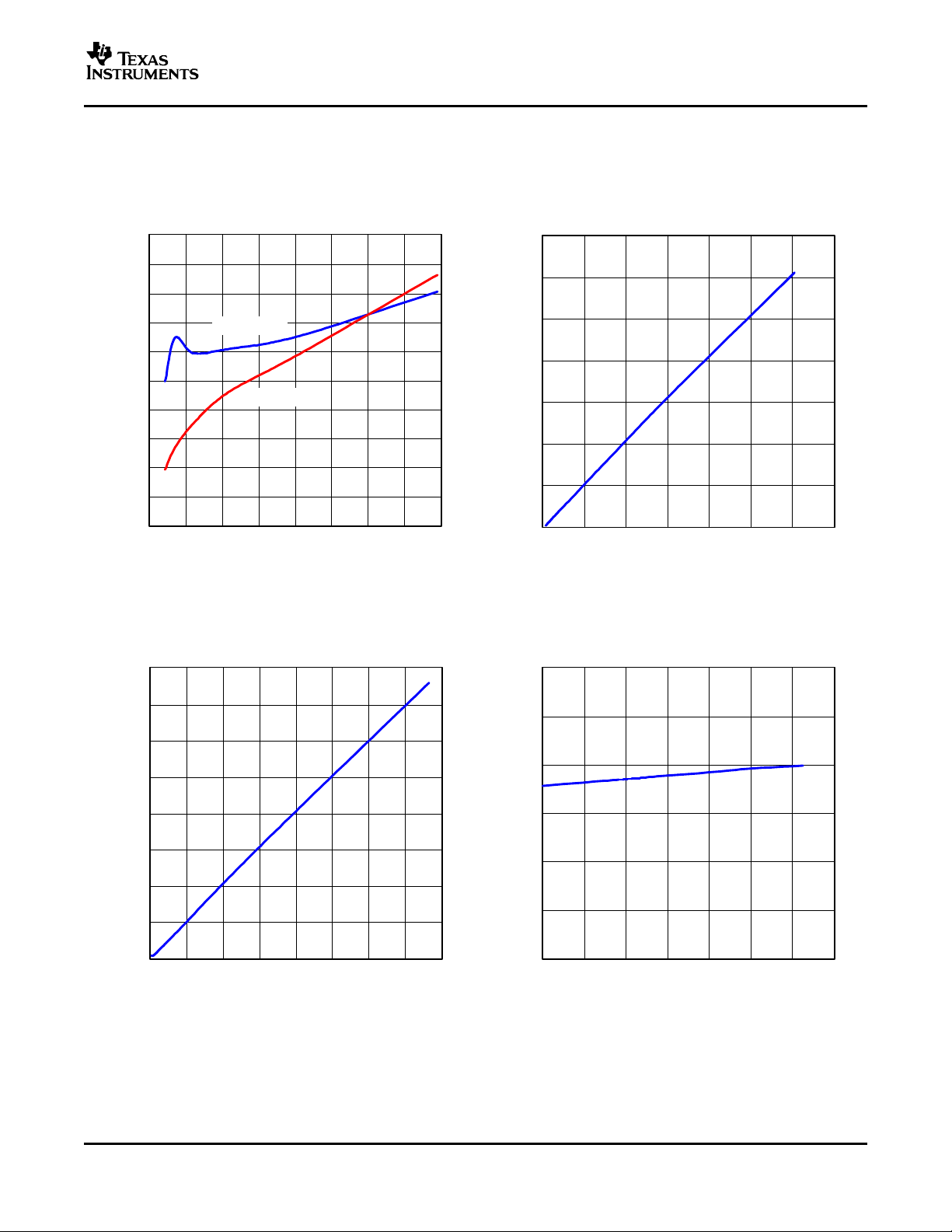
Bias Current − mA
0.0
0.1
0.2
0.3
0.4
0.5
0.6
0.7
0.8
0.9
1.0
0 2 4 6 8 10 12
I
MONB
− Bias-Monitor Current − mA
G001
Modulation Current − mA
0
2
4
6
8
10
12
14
16
0 2 4 6 8 10 12 14 16
Deterministic Jitter − ps
PP
G002
Modulation Current − mA
0.0
0.5
1.0
1.5
2.0
2.5
3.0
0 2 4 6 8 10 12 14 16
Random Jitter − ps
rms
G003
TA − Free-Air Temperature − °C
0.0
0.5
1.0
1.5
2.0
2.5
3.0
−40 −20 0 20 40 60 80 100
Random Jitter − ps
rms
G004
ONET4291VA
SLLS674 – SEPTEMBER 2005
TYPICAL CHARACTERISTICS
Typical operating condition is at V
= 3.3 V and TA= 25 ° C (unless otherwise noted)
CC
BIAS-MONITOR CURRENT I
vs vs
MONB
BIAS CURRENT MODULATION CURRENT
Figure 5. Figure 6.
RANDOM JITTER RANDOM JITTER
vs vs
MODULATION CURRENT TEMPERATURE
DETERMINISTIC JITTER
12
Figure 7. Figure 8.
Page 13
www.ti.com
Modulation Current − mA
0
5
10
15
20
25
30
35
40
45
50
0 2 4 6 8 10 12 14 16
t
t
− Transition T ime − ps
G005
Fall Time
Rise Time
Bias Current Register Setting − mA
0
2
4
6
8
10
12
14
0 2 4 6 8 10 12 14
Open Loop Bias Current − mA
G006
Modulation Current Register Setting − mA
0
2
4
6
8
10
12
14
16
0 2 4 6 8 10 12 14 16
Modulation Current − mA
G007
TA − Free-Air Temperature − °C
20
25
30
35
40
45
50
−40 −20 0 20 40 60 80 100
Supply Current − mA
G008
TYPICAL CHARACTERISTICS (continued)
Typical operating condition is at V
= 3.3 V and TA= 25 ° C (unless otherwise noted)
CC
ONET4291VA
SLLS674 – SEPTEMBER 2005
RISE-TIME AND FALL-TIME BIAS CURRENT IN OPEN LOOP MODE
vs vs
MODULATION CURRENT BASIC REGISTER SETTING
Figure 9. Figure 10.
MODULATION CURRENT SUPPLY CURRENT
vs vs
MODC REGISTER SETTING TEMPERATURE
Figure 11. Figure 12.
13
Page 14
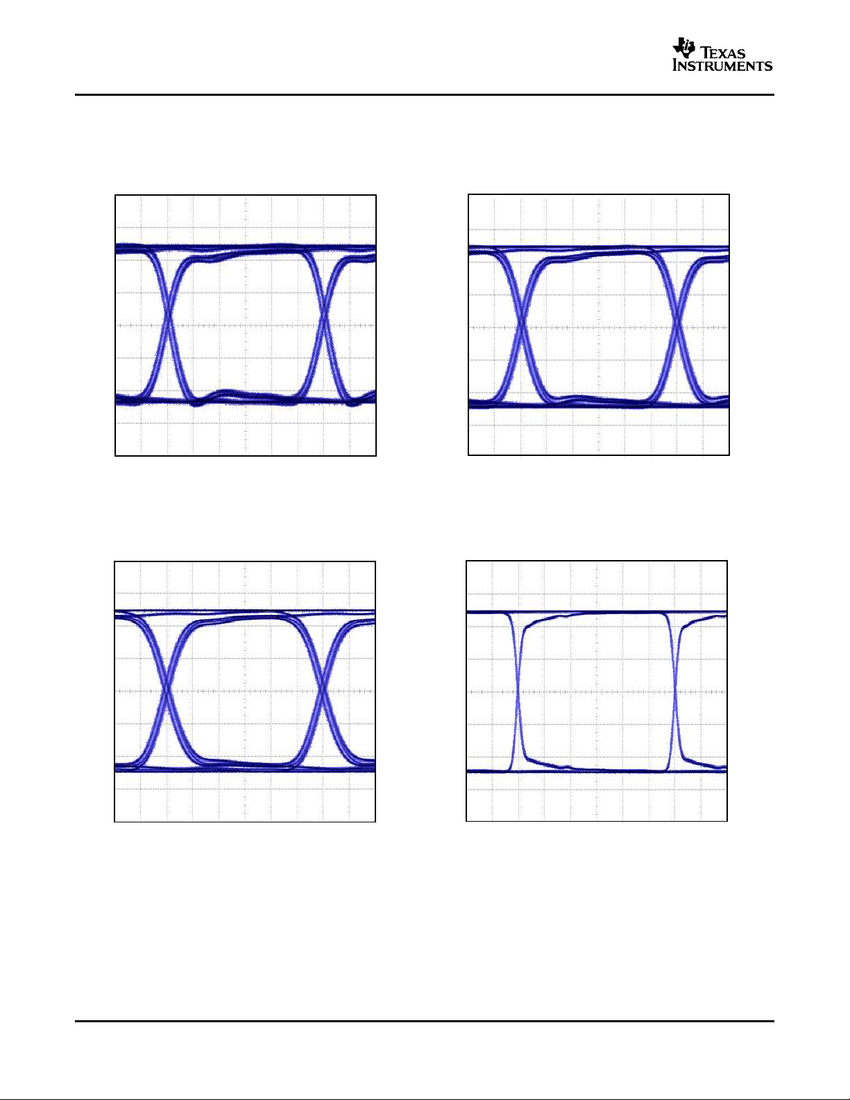
www.ti.com
G009
Single-Ended Output Voltage − 60 mV/Div
t − Time − 40 ps/Div
G010
Single-Ended Output Voltage − 100 mV/Div
t − Time − 40 ps/Div
G011
Single-Ended Output Voltage − 150 mV/Div
t − Time − 40 ps/Div
G012
Single-Ended Output Voltage − 150 mV/Div
t − Time − 157 ps/Div
ONET4291VA
SLLS674 – SEPTEMBER 2005
TYPICAL CHARACTERISTICS (continued)
Typical operating condition is at V
EYE-DIAGRAM AT 4.25 GBPS EYE-DIAGRAM AT 4.25 GBPS
K28.5 PATTERN, I
= 3.3 V and TA= 25 ° C (unless otherwise noted)
CC
= 5 mA K28.5 PATTERN, I
MOD
= 10 mA
MOD
Figure 13. Figure 14.
EYE-DIAGRAM AT 4.25 GBPS EYE-DIAGRAM AT 1.0625 GBPS
K28.5 PATTERN, I
= 15 mA K28.5 PATTERN, I
MOD
Figure 15. Figure 16.
= 15 mA
MOD
14
Page 15

www.ti.com
DIN+
DIN−
VCC
DIS
MONP
SDA
TS
MONB
VCSEL
Laserdiode
Monitor
Photodiode
C3
0.1 µF
FLT
SDK
DIN+
DIN−
MOD+
MOD−
BIAS
GND
VCC
VCC
FLT
ONET4291VA
20-Lead QFN
GND
MONP
CAPC
MONB
VCC
PD
TS
SCK
DIS
SDA
RZTC
50 Ω
L1
BLM15HG102SN1
C4
0.1 µF
R
ZTC
R
MONB
1 kΩ
R
MONP
10 kΩ
C5
0.01 µF
C1
0.1 µF
C2
0.1 µF
S0100-01
30 kΩ
ONET4291VA
SLLS674 – SEPTEMBER 2005
APPLICATION INFORMATION
Figure 17 shows a typical application circuit using the ONET4291VA with a common cathode VCSEL connected
to ground.
The VCSEL driver is controlled via the 2-wire interface SDA/SCK by a microprocessor.
In a typical application, the FLT, MONB, MONP, and TS outputs are connected to the microcontroller for
transceiver management purposes.
The component values in Figure 17 are typical examples and may be varied according to the intended
application.
Figure 17. Basic Application Circuit With a Common Cathode VCSEL
15
Page 16

PACKAGE OPTION ADDENDUM
www.ti.com
28-Sep-2005
PACKAGING INFORMATION
Orderable Device Status
(1)
Package
Type
Package
Drawing
Pins Package
Qty
Eco Plan
ONET4291VARGPR PREVIEW QFN RGP 20 3000 TBD Call TI Call TI
(1)
The marketing status values are defined as follows:
ACTIVE: Product device recommended for new designs.
LIFEBUY: TI has announced that the device will be discontinued, and a lifetime-buy period is in effect.
NRND: Not recommended for new designs. Device is in production to support existing customers, but TI does not recommend using this part in
a new design.
PREVIEW: Device has been announced but is not in production. Samples may or may not be available.
OBSOLETE: TI has discontinued the production of the device.
(2)
Eco Plan - The planned eco-friendly classification: Pb-Free (RoHS) or Green (RoHS & no Sb/Br) - please check
http://www.ti.com/productcontent for the latest availability information and additional product content details.
TBD: The Pb-Free/Green conversion plan has not been defined.
Pb-Free (RoHS): TI's terms "Lead-Free" or "Pb-Free" mean semiconductor products that are compatible with the current RoHS requirements
for all 6 substances, including the requirement that lead not exceed 0.1% by weight in homogeneous materials. Where designed to be soldered
at high temperatures, TI Pb-Free products are suitable for use in specified lead-free processes.
Green (RoHS & no Sb/Br): TI defines "Green" to mean Pb-Free (RoHS compatible), and free of Bromine (Br) and Antimony (Sb) based flame
retardants (Br or Sb do not exceed 0.1% by weight in homogeneous material)
(3)
MSL, Peak Temp. -- The Moisture Sensitivity Level rating according to the JEDEC industry standard classifications, and peak solder
temperature.
(2)
Lead/Ball Finish MSL Peak Temp
(3)
Important Information and Disclaimer:The information provided on this page represents TI's knowledge and belief as of the date that it is
provided. TI bases its knowledge and belief on information provided by third parties, and makes no representation or warranty as to the
accuracy of such information. Efforts are underway to better integrate information from third parties. TI has taken and continues to take
reasonable steps to provide representative and accurate information but may not have conducted destructive testing or chemical analysis on
incoming materials and chemicals. TI and TI suppliers consider certain information to be proprietary, and thus CAS numbers and other limited
information may not be available for release.
In no event shall TI's liability arising out of such information exceed the total purchase price of the TI part(s) at issue in this document sold by TI
to Customer on an annual basis.
Addendum-Page 1
Page 17

PACKAGE OPTION ADDENDUM
www.ti.com
16-Jan-2006
PACKAGING INFORMATION
Orderable Device Status
(1)
Package
Type
Package
Drawing
Pins Package
Qty
Eco Plan
ONET4291VARGPR ACTIVE QFN RGP 20 3000 Green (RoHS &
no Sb/Br)
ONET4291VARGPRG4 ACTIVE QFN RGP 20 3000 Green (RoHS &
no Sb/Br)
ONET4291VARGPT PREVIEW QFN RGP 20 250 Green (RoHS &
no Sb/Br)
(1)
The marketing status values are defined as follows:
ACTIVE: Product device recommended for new designs.
LIFEBUY: TI has announced that the device will be discontinued, and a lifetime-buy period is in effect.
NRND: Not recommended for new designs. Device is in production to support existing customers, but TI does not recommend using this part in
a new design.
PREVIEW: Device has been announced but is not in production. Samples may or may not be available.
OBSOLETE: TI has discontinued the production of the device.
(2)
Eco Plan - The planned eco-friendly classification: Pb-Free (RoHS), Pb-Free (RoHS Exempt), or Green (RoHS & no Sb/Br) - please check
http://www.ti.com/productcontent for the latest availability information and additional product content details.
TBD: The Pb-Free/Green conversion plan has not been defined.
Pb-Free (RoHS): TI's terms "Lead-Free" or "Pb-Free" mean semiconductor products that are compatible with the current RoHS requirements
for all 6 substances, including the requirement that lead not exceed 0.1% by weight in homogeneous materials. Where designed to be soldered
at high temperatures, TI Pb-Free products are suitable for use in specified lead-free processes.
Pb-Free (RoHS Exempt): This component has a RoHS exemption for either 1) lead-based flip-chip solder bumps used between the die and
package, or 2) lead-based die adhesive used between the die and leadframe. The component is otherwise considered Pb-Free (RoHS
compatible) as defined above.
Green (RoHS & no Sb/Br): TI defines "Green" to mean Pb-Free (RoHS compatible), and free of Bromine (Br) and Antimony (Sb) based flame
retardants (Br or Sb do not exceed 0.1% by weight in homogeneous material)
(2)
Lead/Ball Finish MSL Peak Temp
CU NIPDAU Level-2-260C-1 YEAR
CU NIPDAU Level-2-260C-1 YEAR
CU NIPDAU Level-2-260C-1 YEAR
(3)
(3)
MSL, Peak Temp. -- The Moisture Sensitivity Level rating according to the JEDEC industry standard classifications, and peak solder
temperature.
Important Information and Disclaimer:The information provided on this page represents TI's knowledge and belief as of the date that it is
provided. TI bases its knowledge and belief on information provided by third parties, and makes no representation or warranty as to the
accuracy of such information. Efforts are underway to better integrate information from third parties. TI has taken and continues to take
reasonable steps to provide representative and accurate information but may not have conducted destructive testing or chemical analysis on
incoming materials and chemicals. TI and TI suppliers consider certain information to be proprietary, and thus CAS numbers and other limited
information may not be available for release.
In no event shall TI's liability arising out of such information exceed the total purchase price of the TI part(s) at issue in this document sold by TI
to Customer on an annual basis.
Addendum-Page 1
Page 18

Page 19

Page 20
Page 21

IMPORTANT NOTICE
Texas Instruments Incorporated and its subsidiaries (TI) reserve the right to make corrections, modifications,
enhancements, improvements, and other changes to its products and services at any time and to discontinue
any product or service without notice. Customers should obtain the latest relevant information before placing
orders and should verify that such information is current and complete. All products are sold subject to TI’s terms
and conditions of sale supplied at the time of order acknowledgment.
TI warrants performance of its hardware products to the specifications applicable at the time of sale in
accordance with TI’s standard warranty. Testing and other quality control techniques are used to the extent TI
deems necessary to support this warranty. Except where mandated by government requirements, testing of all
parameters of each product is not necessarily performed.
TI assumes no liability for applications assistance or customer product design. Customers are responsible for
their products and applications using TI components. To minimize the risks associated with customer products
and applications, customers should provide adequate design and operating safeguards.
TI does not warrant or represent that any license, either express or implied, is granted under any TI patent right,
copyright, mask work right, or other TI intellectual property right relating to any combination, machine, or process
in which TI products or services are used. Information published by TI regarding third-party products or services
does not constitute a license from TI to use such products or services or a warranty or endorsement thereof.
Use of such information may require a license from a third party under the patents or other intellectual property
of the third party, or a license from TI under the patents or other intellectual property of TI.
Reproduction of information in TI data books or data sheets is permissible only if reproduction is without
alteration and is accompanied by all associated warranties, conditions, limitations, and notices. Reproduction
of this information with alteration is an unfair and deceptive business practice. TI is not responsible or liable for
such altered documentation.
Resale of TI products or services with statements different from or beyond the parameters stated by TI for that
product or service voids all express and any implied warranties for the associated TI product or service and
is an unfair and deceptive business practice. TI is not responsible or liable for any such statements.
Following are URLs where you can obtain information on other Texas Instruments products and application
solutions:
Products Applications
Amplifiers amplifier.ti.com Audio www.ti.com/audio
Data Converters dataconverter.ti.com Automotive www.ti.com/automotive
DSP dsp.ti.com Broadband www.ti.com/broadband
Interface interface.ti.com Digital Control www.ti.com/digitalcontrol
Logic logic.ti.com Military www.ti.com/military
Power Mgmt power.ti.com Optical Networking www.ti.com/opticalnetwork
Microcontrollers microcontroller.ti.com Security www.ti.com/security
Telephony www.ti.com/telephony
Video & Imaging www.ti.com/video
Wireless www.ti.com/wireless
Mailing Address: Texas Instruments
Post Office Box 655303 Dallas, Texas 75265
Copyright 2006, Texas Instruments Incorporated
 Loading...